
 Open Access Article
 This Open Access Article is licensed under a Creative Commons Attribution-Non Commercial 3.0 Unported Licence
Single-molecule quantum tunnelling sensors
Long
Yi†
 ab,
Yuxin
Yang†
a,
Biao-Feng
Zeng†
a,
Xu
Liu
a,
Joshua B.
Edel
c,
Aleksandar P.
Ivanov
*c and
Longhua
Tang
*ab
ab,
Yuxin
Yang†
a,
Biao-Feng
Zeng†
a,
Xu
Liu
a,
Joshua B.
Edel
c,
Aleksandar P.
Ivanov
*c and
Longhua
Tang
*ab
aState Key Laboratory of Extreme Photonics and Instrumentation, Interdisciplinary Centre for Quantum Information, College of Optical Science and Engineering, Zhejiang University, Hangzhou 310027, China. E-mail: lhtang@zju.edu.cn
bNanhu Brain-Computer Interface Institute; Second Affiliated Hospital School of Medicine, Hangzhou, Zhejiang 311100, China
cDepartment of Chemistry, Imperial College London, Molecular Science Research Hub, White City Campus, 82 Wood Lane, W12 0BZ, UK. E-mail: alex.ivanov@imperial.ac.uk
First published on 18th November 2025
Abstract
Single-molecule sensors are pivotal tools for elucidating chemical and biological phenomena. Among these, quantum tunnelling sensors occupy a unique position, due to the exceptional sensitivity of tunnelling currents to sub-ångström variations in molecular structure and electronic states. This capability enables simultaneous sub-nanometre spatial resolution and sub-millisecond temporal resolution, allowing direct observation of dynamic processes that remain concealed in ensemble measurements. This review outlines the fundamental principles of electron tunnelling through molecular junctions and highlights the development of key experimental architectures, including mechanically controllable break junctions and scanning tunnelling microscopy-based approaches. Applications in characterising molecular conformation, supramolecular binding, chemical reactivity, and biomolecular function are critically examined. Furthermore, we discuss recent methodological advances in data interpretation, particularly the integration of statistical learning and machine learning techniques to enhance signal classification and improve throughput. This review highlights the transformative potential of quantum-tunnelling-based single-molecule sensors to advance our understanding of molecular-scale mechanisms and to guide the rational design of functional molecular devices and diagnostic platforms.
 Long Yi | Long Yi is currently a postdoctoral researcher at Zhejiang University. He received his PhD degree from Imperial College London in 2024, where his research was focused on the development of new quantum tunnelling sensors for single molecule detection. His primary research interests include developing new quantum tunnelling platforms and single-molecule electrochemical sensors. |
 Yuxin Yang | Yuxin Yang is currently pursuing her PhD degree at Zhejiang University. She received her BE degree from Zhejiang University in 2023. Her research interests focus on developing next-generation single-molecule intelligent biosensors. |
 Biao-Feng Zeng | Biao-Feng Zeng is currently pursuing his PhD degree at Zhejiang University. He received his BE degree from Chongqing University in 2018 and obtained his MSc degree at Xiamen University in 2021. His research interests focus on quantum tunnelling optoelectronic devices and lightwave electronics techniques. |
 Joshua B. Edel | Professor Joshua Edel is a leading figure in biosensing and analytical sciences at Imperial College London. He earned his PhD in single-molecule detection at Imperial, followed by postdoctoral research at Cornell and Harvard. His research centres on developing advanced analytical platforms for diagnostics, with expertise in single-molecule detection and nanopore sensors. Joshua's work bridges chemistry, physics, and medicine to advance next-generation diagnostic tools. He has published over 180 papers, delivered more than 170 invited talks, received significant funding from the ERC, EPSRC, and Industry, and actively acts as a consultant in biosensing. |
 Aleksandar P. Ivanov | Dr Aleksandar Ivanov is an Associate Professor in the Department of Chemistry and Director of the Network of Electromagnetic and Biochemical Sensors at Imperial College London. He obtained his PhD in Physical Chemistry from Imperial College London in 2012 and holds degrees in Physics and Molecular Biology, as well as formal training in Computer Engineering. His research focuses on the development of nanoscale platforms for single-molecule detection, delivering innovative approaches for direct, label-free sensing of biomarkers across a broad spectrum of conditions, including various cancers, cardiovascular disease, neurodegenerative disorders, and infectious diseases. |
 Longhua Tang | Professor Longhua Tang received his BS in 2005 from Hefei University, MSc in 2008 from East China University of Science and Technology, and PhD in 2013 from Tsinghua University. He joined the College of Optical Science and Engineering at Zhejiang University as an Associate Research Professor, becoming an Associate Professor in 2016 and a Professor in 2023. He was a visiting scholar at the University of Illinois at Urbana–Champaign (2010–2012) and Imperial College London (2018–2019). He currently leads an interdisciplinary group focused on Bio-Opto-Electronic (BOE) technologies, with research spanning-quantum biosensors, single-molecule intelligent detection and related applications. |
1. Introduction
Single-molecule sensors have emerged as powerful analytical tools for investigating chemical and biological processes at the molecular level. By detecting individual molecules, these sensors provide a way to reveal molecular heterogeneity, transient intermediates, and dynamic processes that are difficult to identify using traditional methods. These sensors can provide detailed insights into the fundamental mechanisms of chemical reactions, biological interactions, and molecular-scale structural changes. This detailed understanding is particularly valuable for applications in catalysis, drug discovery, clinical diagnostics, and fundamental biochemical research.Among the various single-molecule detection strategies, quantum tunnelling sensors stand out for their exceptional spatial resolution, sensitivity, and chemical specificity. These platforms operate by applying a voltage bias across two closely spaced electrodes, allowing electrons to tunnel through a molecular junction. The resulting tunnelling current is highly sensitive to the width of the gap, the applied potential, and the properties of the medium within the junction.1,2 This sensitivity enables the direct detection of individual molecules without the need for labelling. Quantum tunnelling sensors also benefit from high-bandwidth measurements, spanning the kilohertz (kHz) to megahertz (MHz) range, which enables real-time tracking of molecular changes at the sub-microsecond timescale.3 As a result, tunnelling sensors can serve as a new single-molecule detection platform, allowing for the direct label-free, real-time detection of individual molecules.4
Quantum tunnelling offers a direct pathway to access molecular information from a single entity, which is otherwise inaccessible due to ensemble averaging. This ability facilitates the development of single-molecule electronics, where molecular-scale changes such as conformational shifts, orbital reorganisation, and intramolecular vibrations are directly reflected in tunnelling current responses. Since the pioneering theoretical work by Aviram and Ratner on molecular junctions,5 the field has seen remarkable progress in device fabrication and measurement techniques. Scaling devices down to the single-molecule level marks a conceptual frontier, enabling the exploitation of molecular structural and electronic properties for functional applications. By transforming subtle structural changes into distinct electronic outputs, single-molecule electronics opens new possibilities for functional devices and sensing platforms operating at the single-molecule level. To date, a variety of quantum tunnelling platforms, including scanning tunnelling microscopy-break junctions (STM-BJs), mechanically controllable break junctions (MCBJs), and static molecule junctions, have provided multiple options for monitoring single-molecule behaviours.6 The integration of various optimisation techniques, such as chemical functionalisation, electrochemical setups, and optical monitoring, has expanded the capabilities of tunnelling sensors to investigate molecular structures, chemical reactions, and biological functions.7,8
In this review, we provide a comprehensive assessment of quantum tunnelling-based platforms for single-molecule detection, with an emphasis on both technological advancements and mechanistic insights (Fig. 1). We begin by discussing fabrication strategies and comparative performance metrics, including resolution, stability, and scalability. We then discuss the application of tunnelling sensors in elucidating molecular mechanisms, structural transitions, and dynamic interactions at the single-molecule level. Finally, we consider the broader implications of these developments for molecular-scale electronics, the understanding of reaction pathways, and the future of next-generation biosensing technologies.
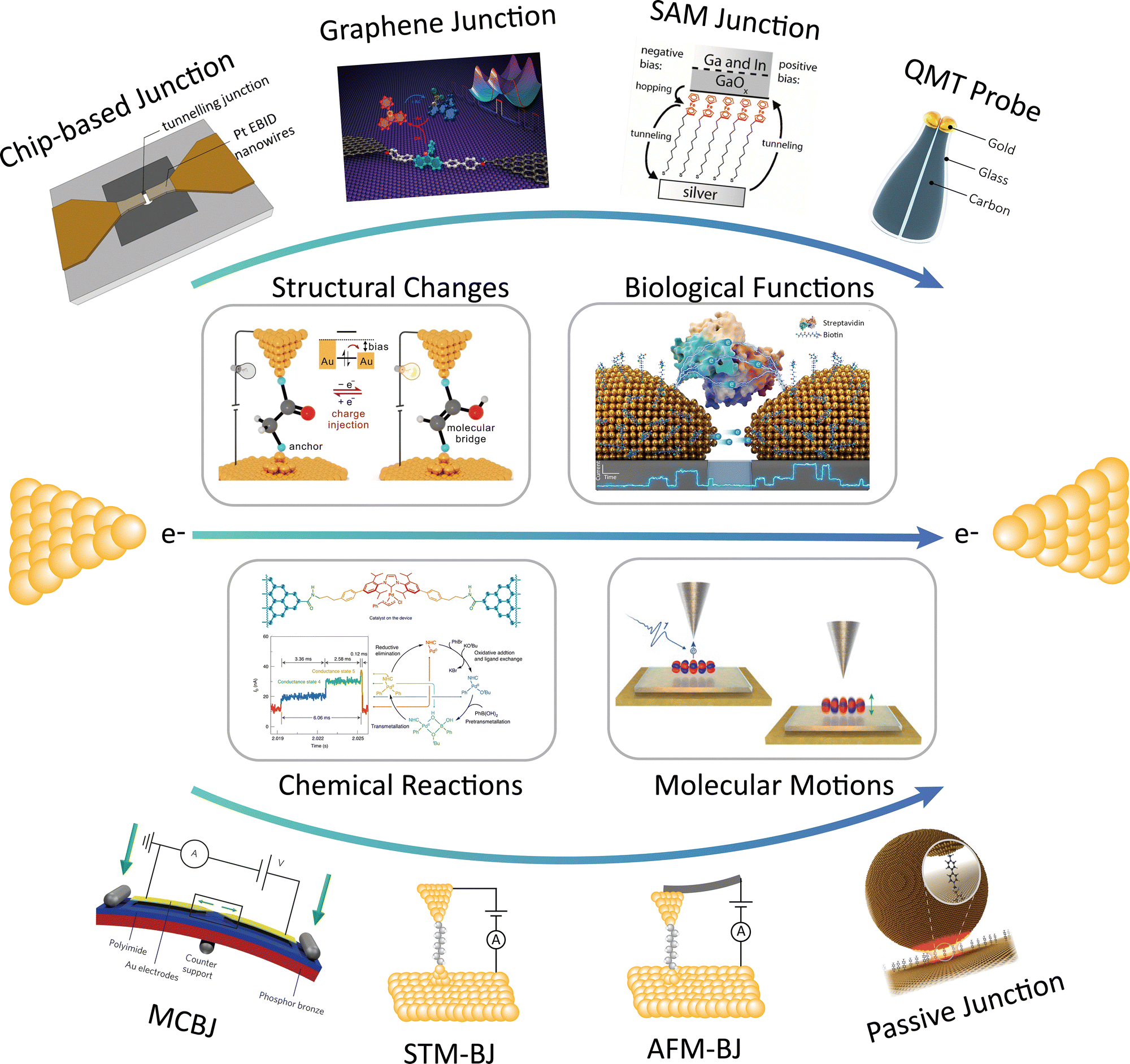 | ||
| Fig. 1 Schematic illustration of current quantum tunnelling platforms, along with applications. Panel (tunnelling junction with nanopore) is reprinted with the permission from ref. 277, Copyright (2014), American Chemical Society. Panel (graphene molecular junction) is reprinted with the permission from ref. 265, Copyright (2018), American Chemical Society. Panel (EGaIn junction) is reprinted with the permission from ref. 48, Copyright (2010), American Chemical Society. Panel (MCBJ) is reprinted with the permission from ref. 27, Copyright (2013), Springer Nature. Panel (Passive junction) is reprinted with the permission from ref. 130, Copyright (2017), Springer Nature. Panel (structural change) is reprinted with the permission from ref. 167, Copyright (2023), Springer Nature. Panel (biological functions) is reprinted with the permission from ref. 85, Copyright by Longhua Tang (2022), under CC BY 4.0 license. Panel (chemical reactions) is reprinted from ref. 266, Copyright (2021), Springer Nature. Panel (molecular motion) is reprinted with the permission from ref. 191, Copyright (2016), Springer Nature. | ||
2. Theory and principle for designing single-molecule quantum tunnelling sensors
2.1. Quantum tunnelling effect
When two electrodes are separated by an insulating layer at a nanometre-scale distance, the electrical behaviour of molecules no longer follows Ohm's law. At this scale, quantum effects begin to significantly influence the charge transport of molecules. Electrons with particular energies are able to tunnel through an insulator and flow into the conduction band.9 This phenomenon is known as quantum tunnelling. In 1963, the Simmons model was developed to quantify this effect.10When a voltage bias is applied between two electrodes, the potential difference not only distorts the potential barrier but also provides energy for electrons to tunnel through the insulator.11 Thus, the tunnelling effect can be classified into three regimes based on the shape of the energy barrier, as shown in Fig. 2: (a) Zero bias. When no potential difference exists between the electrodes, the energy barrier is rectangular. (b) Low bias. A small voltage transforms the barrier into a trapezoidal shape. In this regime, the tunnelling current (I) under an applied voltage V can be approximated by:
 | (1) |
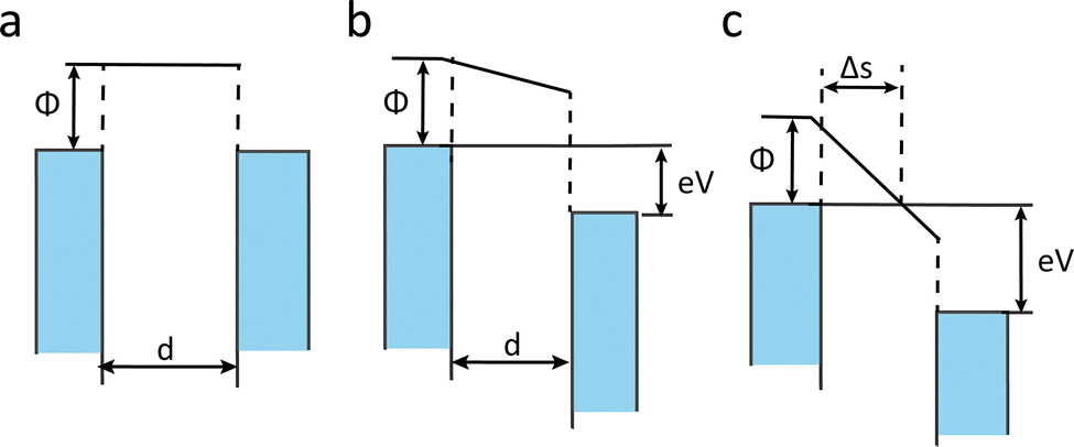 | ||
| Fig. 2 The schematic diagram of the Simmons Model with (a) rectangular, (b) trapezoidal and (c) triangular barrier height. | ||
2.2. Tunnelling through a molecule
To understand electron transport, we begin by examining a simple molecular junction, where a single quantum wire bridges two electrodes separated by a distance L. In macroscopic conductors, electrons typically move between electrodes through a process known as classical diffusion. When L is reduced to the scale of a single molecule, classical diffusion no longer adequately describes electron transport. Instead, electrons pass through quantum tunnelling. Depending on the distance between the mean free path ℓ and L, the electrode tunnelling can be classified as diffusion transport and ballistic transport. As illustrated in Fig. 3(a), when L is larger than ℓ, the electron tunnelling process is dominated by diffusion transport. When L is smaller than ℓ, the ballistic transport dominates the electron tunnelling process as shown in Fig. 3(b), and this process can be described by the Landauer equation.14 When a ballistic quantum point contact bridges in the tunnelling junction, the electrons with a certain energy E have a probability T(E) to tunnel through the nanogap under the voltage bias V.14–16 The conductance G can be calculated by eqn (2):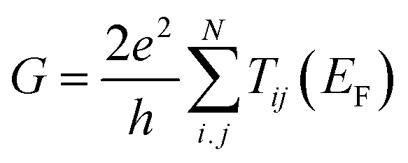 | (2) |
G = G0![[thin space (1/6-em)]](https://www.rsc.org/images/entities/char_2009.gif) exp(−βTd) exp(−βTd) | (3) |
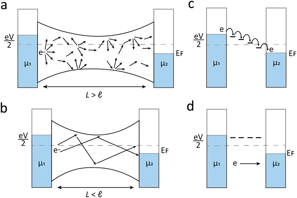 | ||
| Fig. 3 Schematic diagram of (a) diffusion transport, (b) ballistic transport, (c) hopping tunnelling and (d) coherent tunnelling. | ||
When a molecule is placed between the tunnelling junction, electron transport becomes more complex due to molecular properties, electrode–molecule coupling, and the molecule's structure. The conductance in such cases is expressed as:
| G = Aexp(−β1l) | (4) |
When a molecule is incorporated into the junction, frontier molecular orbitals can facilitate electron transfer. If there is no phase-coherence-breaking process in the molecule, this process is referred to as coherent tunnelling. As shown in Fig. 3(d), in this situation electrons can tunnel directly from one electrode to the other without inelastic interactions molecule. Coherent tunnelling typically occurs over short tunnelling distances or through the molecule with large highest occupied molecular orbitals (HOMO)–lowest unoccupied molecular orbitals (LUMO) gaps.19 Coherent tunnelling can be described by two models: direct tunnelling (superexchange) at low voltages, and Fowler–Nordheim tunnelling (field emission) at higher voltages. While direct tunnelling follows the simplified Simmons model, field emission is best described by the Fowler–Nordheim relation20,21
 | (5) |
In contrast, incoherent tunnelling occurs when electrons interact with electrons in molecules and change the electron phase. The main mechanism of the incoherent tunnelling process can be illustrated by the hopping model shown in Fig. 3(c), in which electrons move between orbitals step-by-step across the molecule. Hopping typically occurs in longer molecules with smaller HOMO–LUMO gaps or smaller energy barriers between transport orbitals and the Fermi level. This process is thermally activated, requiring electrons to overcome activation energy, described by the Arrhenius equation (eqn (6)):
 | (6) |
In incoherent tunnelling, conductance strongly depends on temperature T and weakly on tunnelling distance, typically varying inversely with molecular length.21,22 Therefore, analysing the temperature dependence of tunnelling current is a reliable method for distinguishing between coherent and incoherent transport mechanisms.
2.3. Quantum interference
When an electron travels through a molecule via quantum tunnelling, the wave-like properties of electrons allow propagation along multiple pathways within the molecule. During this process, the electron wavefunction may interact with the molecular orbitals, resulting in interference effects known as quantum interference.23Quantum interference is primarily classified as constructive and destructive interference, based on the relative alignment of electron wave phases, and can be observed using transmission spectroscopy. Constructive quantum interference (CQI) increases electron transmission probability, resulting in smoother transmission curves upon superposition. Conversely, destructive quantum interference (DQI) reduces electron transmission, often generating sharp anti-resonance peaks near the electrode Fermi level.24
Beyond transmission probability, quantum interference significantly influences molecular conductance. Hong et al. experimentally demonstrated this effect by comparing the conductance of anthracene-, anthraquinone-, and dihydroanthracene-based linearly conjugated wires using MCBJs.25 Variations in molecular orbitals resulting from changes in molecular conformation or electrode Fermi levels have a significant impact on interference patterns. Consequently, tuning molecular structure or electrode conditions offers a viable strategy for optimising quantum interference effects.
In addition to CQI and DQI, Fano resonance represents another form of quantum interference. This phenomenon occurs when a discrete quantum state interferes with a continuum of states, resulting in enhanced gate modulation over narrow voltage ranges. Fano resonance produces an asymmetric line shape in transmission spectra and has been experimentally observed by Zhang et al. using STM-BJs.26 Through the integration of electrochemical gating, the para-carbazole anion can be transferred between redox states, resulting in a switch from resonance to anti-resonance. By modulating quantum interference, different molecular device functions can be achieved, and quantum interference may hold significant potential for the development of high-performance molecular devices.
3. Fabrication of quantum tunnelling research platform
The fabrication of nanogap electrodes within the quantum tunnelling regime is a critical prerequisite for constructing reliable single-molecule tunnelling sensors. Creating nanogaps below 5 nm presents substantial challenges in terms of reproducibility, mechanical stability, and dimensional control. However, recent advances in nanofabrication have yielded several experimental strategies to address these limitations. Key techniques include mechanically controllable break junctions,27,28 scanning tunnelling microscope break junctions,29 electromigration-induced break junctions,30 photolithographic methods,31 magnetically controlled cross-wire junctions,32 and feedback-driven electrochemical deposition.33,34 These approaches have played a vital role in translating quantum tunnelling concepts from theoretical models into practical, reproducible experimental platforms. Based on the junction configuration, quantum tunnelling platforms can be broadly categorised as static, dynamic, and passive junctions.3.1. Static tunnelling junctions
Static tunnelling junctions maintain a fixed interelectrode separation, typically supported by a mechanically rigid structure. Their fabrication methods can be broadly divided into additive and subtractive approaches. Additive methods involve progressively depositing conductive material onto electrodes initially spaced farther apart, thereby narrowing the gap with precise control. In contrast, subtractive methods create nanogaps by selectively breaking or etching a continuous conductive layer. Both strategies offer promising routes to developing chip-based, high-throughput platforms that enable multiplexed single-molecule measurements with improved stability and scalability.One widely adopted approach is thermal evaporation, first introduced by Dolan's group in 1977.39,40 As illustrated in Fig. 4(a), the process begins with a wider nanogap formed via electron-beam lithography. The gap is then progressively reduced by depositing a thin metallic layer under high vacuum and elevated temperatures.35 This technique enables the fabrication of a wide range of nanogap electrodes with widths below 5 nm.
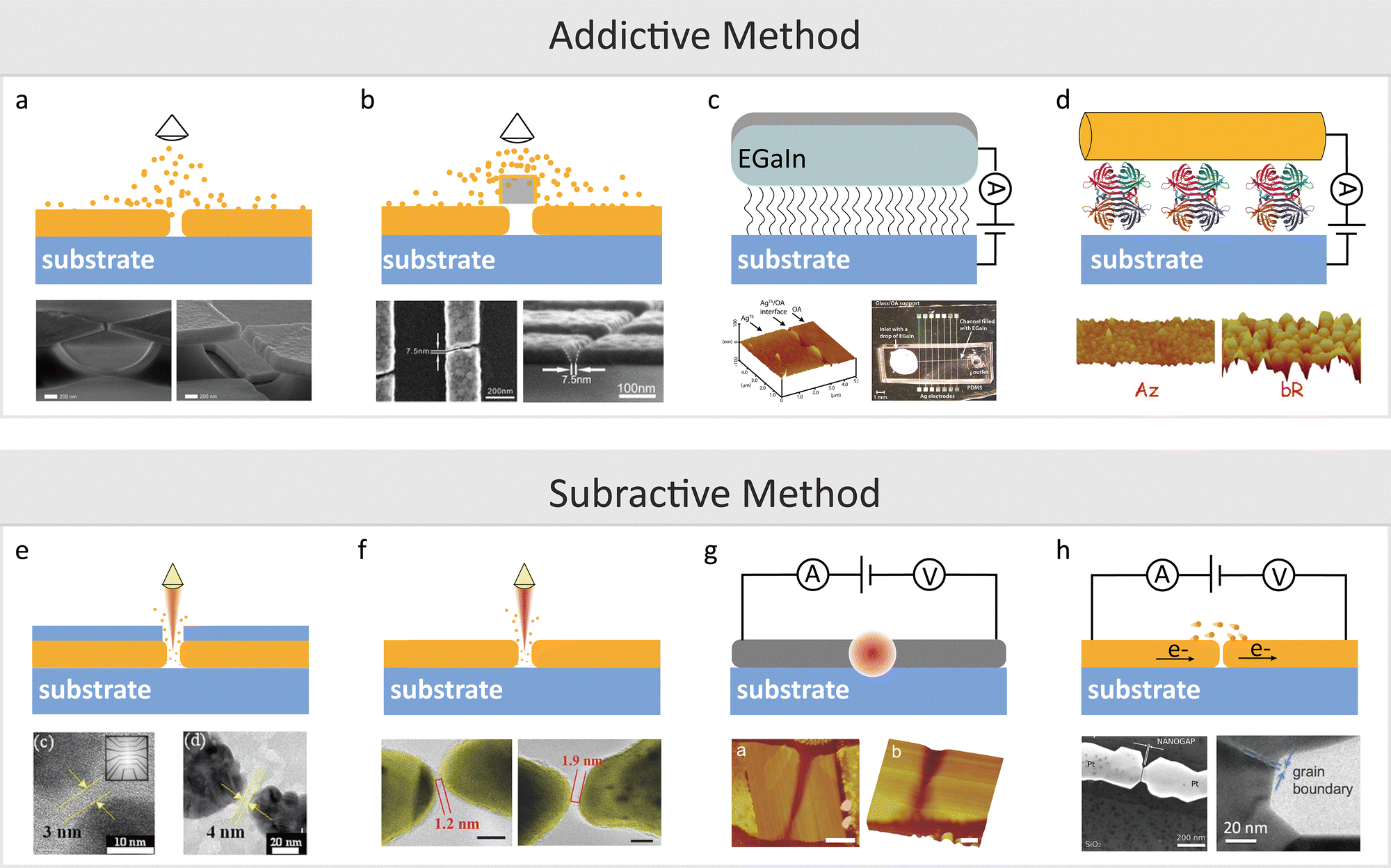 | ||
| Fig. 4 Methods for fabricating quantum tunnelling platforms and their corresponding junction geometries. (a) Vaporisation deposition of a nanogap on the substrate. The initial gap, which is large, is created using electron beam lithography, and vapour deposition reduces the gap to below 5 nm. (b) Vaporisation deposition with a shadow mask. The mask is placed on top of the nanogap during vapour deposition, shaping the gap whose width depends on the mask size. (c) Nanogap formation via SAM and liquid metal. A SAM monolayer is applied to the conductive substrate, and liquid metal (Ga/In) is deposited at top to form a metal-SAM-substrate tunnelling junction. (d) Protein monolayer junction. The protein monolayer is first created on a gold (Au) substrate, followed by the deposition of an Au nanowire to produce an Au-protein-Au junction. (e) Nanogap via electron beam lithography. An Au layer is deposited on the substrate and coated with resist. Electron beam lithography then carves the gap into the resist to form the tunnelling junction. (f) Nanogap using focused ion beam lithography. An Au layer is deposited on the substrate, and a focused ion beam is used to directly create a nanogap. (g) Graphene nanogap via feedback-controlled electroburning. A graphene monolayer is deposited on the substrate, and a gap is formed by applying cyclic voltammetry with increasing voltage to break the graphene. (h) Nanogap by electromigration. Metal atoms are moved by high electrical current density and concentrated Joule heat. Panel (a) is reprinted with permission from ref. 35, Copyright (2012), AIP Publishing. Panel (b) is reprinted with permission from ref. 42, Copyright (2019), American Chemical Society Panel (c) is reprinted with permission from ref. 48, Copyright (2010), American Chemical Society Panel (d) is reprinted with permission from ref. 53, Copyright (2010), American Chemical Society. Panel (e) is reprinted with permission from ref. 58, Copyright (2006), AIP Publishing. Panel (f) is reprinted with permission from ref. 63, Copyright (2015), Wiley-VCH Verlag GmbH & Co. KGaA, Weinheim. Panel (g) is reprinted with permission from ref. 65 Copyright (2011), American Chemical Society Panel. (h) is reprinted with permission from ref. 69, Copyright (2012), American Chemical Society. | ||
To accurately control the gap distance during vaporisation deposition, a shadow mask is employed to block deposition areas and create the nanogap selectively. As shown in Fig. 4(b) the gap distance depends on the mask width, deposition angle, and grain size of the deposited material. Currently, gaps ranging from 0.8 nm to 5 nm can be reliably fabricated by adjusting deposition angles and selecting appropriate mask materials, such as conventional shadow masks and single-walled carbon nanotubes.41–44
An alternative approach, surface-catalysed chemical deposition, offers a wet-chemistry-based route to electrode fabrication directly on substrates. In this method, the mild reduction of metal precursors in solution enables the gradual deposition of conductive material onto the electrode edges. The final nanogap width can be adjusted by varying the reaction time, temperature, and precursor concentration.36,45 With the aid of electron-beam lithography, Chil et al. successfully applied this technique to achieve gaps as small as 1 nm.36 Serdio et al. introduced self-assembled monolayers (SAMs) of alkyl chains on electrode surfaces. By varying the alkyl chain length (C12–C18), they achieved precise tuning of gap distances from 2.5 to 3.3 nm.38
Another notable configuration is the vertical tunnelling junction, in which a molecule is sandwiched between two electrodes. This architecture allows symmetric or asymmetric setups using different top contact materials. The concept was demonstrated by Haag et al. using a Hg–SAM/SAM–Hg junction, where the SAM layer defined the insulating barrier and controlled the gap distance.46 To address mercury's toxicity and instability, eutectic gallium–indium (EGaIn) alloys have emerged as safer alternatives. EGaIn forms a surface oxide Ga2O3, which prevents penetration and enhances stability.47 Whitesides’ group developed the EGaIn–SAM–Au junction, illustrated in Fig. 4(c), where droplets of liquid metal gently contact SAM-modified surfaces to form stable, large-area molecular junctions.46,48,49 These liquid-based junctions are particularly effective for ensemble-level charge transport studies in well-defined molecular layers.
In addition to liquid metals, solid metals such as Pb, Au, Ag, and Ti can be deposited onto SAM layers using physical vapour deposition (PVD), enabling tailored junctions for applications including charge transport, rectification, and molecular switching.50–52 Beyond deposition, nanowires offer an alternative route for constructing conductive layers. Cahen's group developed a method where a protein layer acts as a tunnelling barrier on an Au substrate.53 As shown in Fig. 4(d), an Au nanowire is deposited atop the protein to form a suspended Au–protein–Au contact.47,54–56 This approach avoids common drawbacks of atomic-scale fabrication, such as structural defects, mechanical damage, and chemical degradation.57 It also eliminates the need for covalent bonding between SAM molecules and the top electrode, thereby preserving the native molecular structure and making it particularly suitable for protein-based studies.
Focused ion beam (FIB) lithography offers a maskless alternative for the direct fabrication of nanogaps with reduced proximity effects compared to EBL.62 The typical experimental configuration is shown in Fig. 4(f).63 Li et al. demonstrated the fabrication of nanogaps ranging from sub-3 nm to 30 nm, with in situ electrical monitoring allowing precise control over gaps between 3 and 6 nm.64 FIB can produce gaps as small as 1.2 nm, offering high reliability and resolution, making it a promising technique for nanogap electrode fabrication.
Beyond lithographic methods, fixed nanogaps can also be formed through electrothermal and electrochemical breakdown techniques. In 2011, Prins et al. reported the fabrication of graphene nanogap electrodes via feedback-controlled electroburning, as shown in Fig. 4(g).65 By repeatedly sweeping the voltage across graphene nanowires, controlled breakdown occurs due to Joule heating, which is monitored via the current–voltage response. Electromigration methods apply high current densities to induce atomic movement along the direction of electron flow, causing gap formation.66,67Fig. 4(h) shows a typical schematic of this approach. The formation of a nanogap can be monitored and confirmed by the appearance of a sigmoidal I–V curve. This technique can fabricate nanogap electrodes smaller than 2 nm.68,69 Additionally, repeated electromigration can shrink the gap to a few ångströms, enabling the reversible opening and closing of atomic-scale contacts.68,70,71
In addition to metallic electrodes, carbon-based materials such as single-walled carbon nanotubes (SWNTs) and graphene are highly suitable for quantum tunnelling sensors due to their excellent electrical conductivity, mechanical robustness, and thermal stability. Compared to metals, carbon materials offer superior chemical compatibility with organic molecules, facilitating coupling via π–π interactions and covalent bonding.72 In 2004, Qi et al. reported the application of electrical breakdown to SWNTs and the fabrication of nanogap electrodes with a 6 nm width.73 Later, in 2006, Guo et al. applied local oxygen plasma etching through a photolithographically defined PMMA window to create nanogaps in SWNTs, as shown in Fig. 5(a).31 Moreover, this process not only forms the nanogap but also oxidises the surface to carbonyl groups, further reducing the gap distance and enabling molecular capture to form a CNT–single-molecule–CNT junction. These methods enable sub-10 nm electrode separations with controlled geometries. Furthermore, functionalising CNTs with various anchoring groups enables the detection of a wide range of single molecules, including targets such as enzymes and proteins.74 FIB techniques have also been applied to break CNTs with nanometre precision, offering another route to fabricate single-molecule junctions.75,76
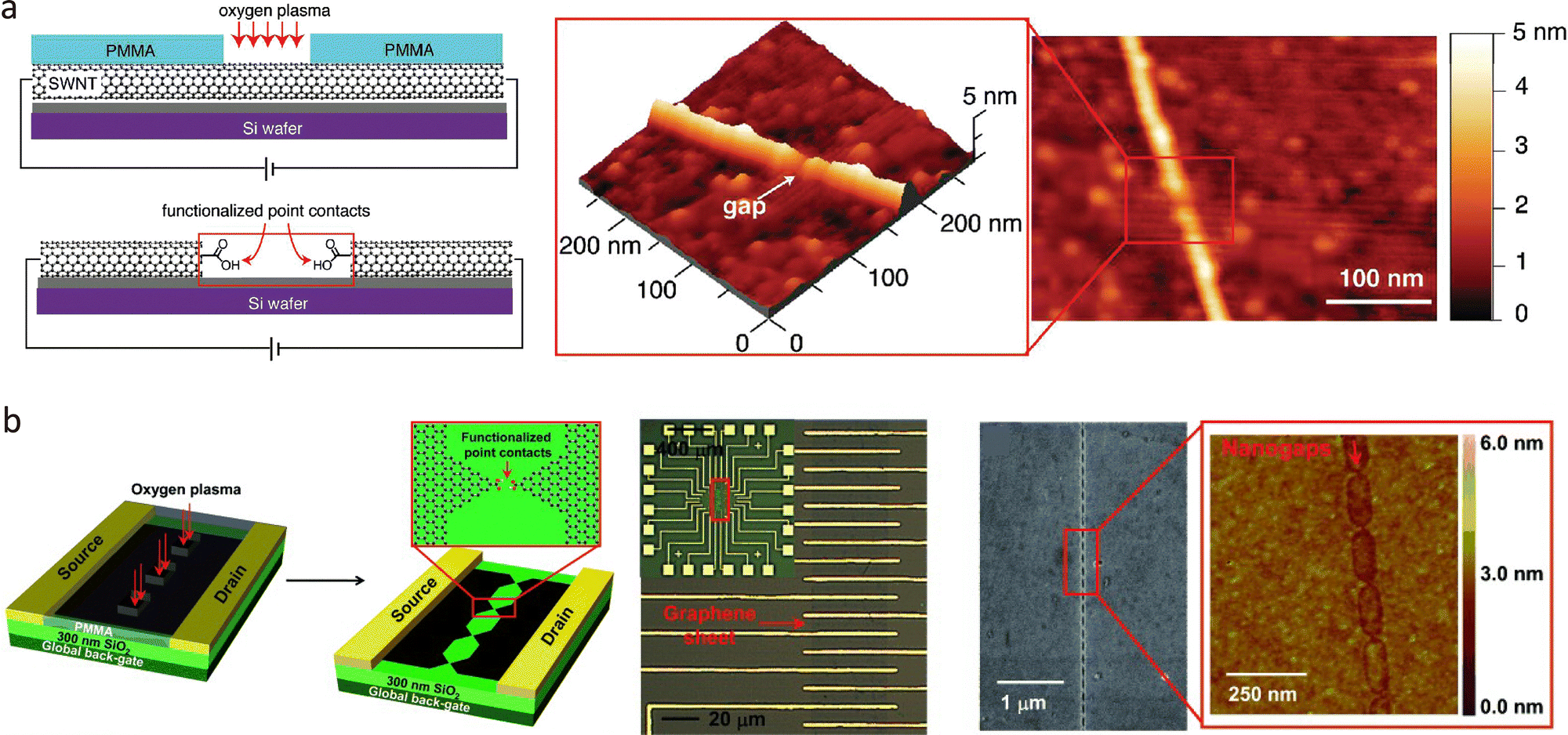 | ||
| Fig. 5 Carbon-based nanogap electrodes. (a) Fabrication of the carbon nanogap electrodes through oxygen plasma etching. The AFM image shows the nanogap configuration. (b) Fabrication of a graphene nanogap electrode array through dotted line lithography-defined oxygen plasma oxidative-etching process. The SEM and AFM images show the configuration of the graphene nanogap electrode. Panel (a) is reprinted with permission from ref. 31, Copyright (2006), American Chemical Society. Panel (b) is reprinted with permission from ref. 78, Copyright (2012), Wiley-VCH Verlag GmbH & Co. KGaA, Weinheim. | ||
Graphene is a carbon nanomaterial with a two-dimensional structure and superior electronic properties, enabling planar molecular junctions with nanometre precision and scalable array formats.77 Similar to CNTs, fabrication strategies, including feedback-controlled electroburning, oxygen plasma etching, and hybrid lithography, can be applied to fabricate nanogap electrodes. The first graphene tunnelling junction was reported using controllable electroburning.65 In 2012, Guo et al. applied oxygen plasma etching to single-layer graphene sheets to produce nanogap arrays using dot-line lithography, as shown in Fig. 5(b).78 Similar to CNT fabrication, the PMMA array windows were fabricated through photolithography, and the oxygen plasma was applied to form sub-10 nm nanogap arrays with carboxyl terminal groups. This technique can fabricate functionalised nanogap electrodes with a yield of up to 50%. Moreover, combining lithography-defined plasma etching with feedback-controlled electroburning increased the yield to 71%, enabling large-scale, integrated graphene electrode arrays for single-molecule studies.79
In 2001, Tao et al. reported a bi-potentiostatic feedback-controlled deposition technique, as shown in Fig. 6(a).33 Electrodes were held at constant potential during deposition, while a voltage bias was applied to monitor tunnelling junction formation. The tunnelling current was continuously recorded, revealing a characteristic exponential increase in conductance spanning three to four orders of magnitude as the gap narrowed. This stepwise increase reflects the atom-by-atom nature of junction formation.
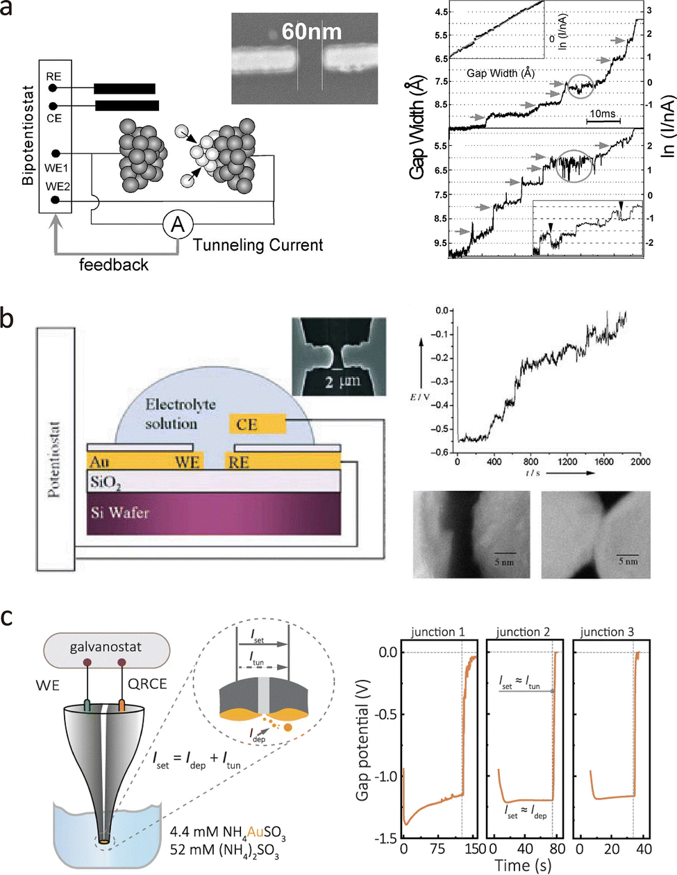 | ||
| Fig. 6 Nanogap fabrication via electrochemical methods. (a) Schematic illustration (left) of the experimental setup. The right panel shows typical gap distance-time and current–time responses. (b) Galvanostatic feedback control deposition of nanogap electrodes. The right panel displays a typical voltage-time response and an SEM image of the nanogap. (c) Galvanostatic feedback control deposition of Au on the dual-barrel carbon nanoelectrodes. The right panel illustrates the typical voltage-time feedback control configuration. Panel (a) is reprinted with permission from ref. 33, Copyright (2000), AIP Publishing. Panel (b) is reprinted with permission from ref. 81, Copyright (2005), Wiley-VCH Verlag GmbH & Co. KGaA, Weinheim. Panel (c) is reprinted with permission from ref. 34, Copyright (2021), Springer Nature. | ||
Alternatively, Li et al. employed the galvanostatic method to fabricate nanogap electrodes, as illustrated in Fig. 6(b).81 A constant current Iset was applied between two Au nanoelectrodes, while one electrode acted as a working electrode and the other electrode acted as a quasi-reference/counter electrode (QRCE). The interelectrode voltage (Vgap) was monitored to regulate the electrodeposition process. According to the Guoy–Chapman–Stern (GCS) model,82 when the gap narrowed due to deposition on the WE, the overlapping of the double layer at the WE results in a sudden decrease in Vgap.81 By terminating the deposition at a specific Vgap, reproducible nanogaps with sub-nanometre to approximately 3 nm separation can be fabricated.83
Beyond on-chip devices, this method is also applicable to probe-based tunnelling platforms. Tang et al. fabricated tunnelling electrodes on dual-barrel quartz–carbon nanoelectrodes using feedback-controlled electrodeposition, as shown in Fig. 6(c).34,84 These electrodes can detect freely diffusing single molecules, such as redox-active species, ssDNA, and proteins, in solution. Functionalisation with anchoring groups (e.g., biotin) enables the capture of specific targets, such as streptavidin, forming single-protein junctions.85 This probe-like geometry also holds promise for in vivo detection, with potential applications in early diagnostics and real-sample analysis.
A key challenge in electrodeposition is the rapid exponential increase in current, which can lead to reconnection of the nanogap. To address this, electrochemical breakdown techniques have been developed to regenerate nanogaps and improve fabrication yield. For example, Tang et al. applied electrochemical etching to break connections between Au nanoelectrodes and dual-barrel quartz–carbon probes.86 Selective etching in a KCl/K2S2O3 electrolyte under controlled voltage conditions was monitored via current–time measurements, where a sharp current drop indicated successful gap formation. This method offers a reproducible, cost-effective strategy for regenerating nanogap electrodes, thereby enhancing overall fabrication efficiency.
In STM-FJs, a metallic STM tip and substrate are positioned to form a nanogap that, once bridged by a molecule, remains fixed. This setup provides a mechanically stable platform for long-duration conductance measurements. I–t traces obtained in this mode reveal intrinsic charge transport characteristics and dynamic molecular behaviour, although junction drift and interface fluctuations may still affect stability.87 Similarly, AFM-FJs employ a conductive AFM cantilever and a substrate electrode to form the nanogap, enabling stable molecular contact. This configuration enables simultaneous measurement of electrical conductance and mechanical parameters, including rupture force, stretching length, and junction stiffness. By combining I–t monitoring with force spectroscopy, AFM-FJs offer correlated insights into the electronic and mechanical responses of single molecules.88
Both STM-FJs and AFM-FJs provide robust platforms for constructing long-lived single-molecule junctions. Their ability to maintain stable contact under static conditions enables the acquisition of single-molecule information with improved reproducibility and extended measurement lifetimes.89
3.2. Dynamic tunnelling junctions
Dynamic tunnelling junctions are characterised by their formation through mechanical displacement of electrode pairs, typically transitioning from contact to separation. As the electrodes are pulled apart, a nanogap forms within the tunnelling distance regime (typically <2 nm), allowing single-molecule conductance measurements when target molecules are tethered to one electrode. The molecular bridge forms during retraction, enabling the detection of electronic and mechanical signatures from individual molecules. Unlike static junctions, dynamic break junctions not only resolve conductance but also provide access to distance-dependent transport properties, revealing insights into molecular stretching, conformation, and electrode–molecule coupling. However, at the single-molecule scale, variations in device configuration, electrode surface functionalisation, and local environment can lead to significant changes in conductance during measurement. Even for the same molecule, it is challenging to ensure an identical connection process during the measurement. Therefore, instead of obtaining conductance information from a single molecule, the repeated formation and breaking of thousands of such junctions yield statistically robust single-molecule conductance-distance histograms, providing the most likely conductance of the target analyte and supporting high-throughput probing of molecular behaviour under nanoconfinement.90,91Since then, STM-BJ techniques have been widely applied to the study of single-molecule properties by monitoring changes in conductance. Fig. 7(a) illustrates the configuration and main experimental setup of the STM-BJ. Depending on whether the tip interacts with the substrate during movement, STM-BJ experiments are generally classified into two modes: hard-contact and soft-contact modes, as shown in Fig. 7(b) and (c). In the hard-contact mode, the metallic tip (typically gold) makes direct contact with the substrate and is then retracted, leading to atomic-scale thinning and the formation of a single-atom contact prior to rupture. In the soft-contact mode, the tip is suspended close to the substrate. The molecules can diffuse into the nanogap and are transiently trapped during tip retraction. By pulling the tip to break the single-molecule contact, current–distance (I–z) responses can be recorded to provide insight into single-molecule behaviour.2
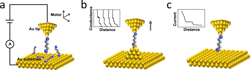 | ||
| Fig. 7 (a) The schematic illustration of the typical STM-BJ experimental setup. The single-molecule conductance can be measured via (b) hard-contact mode and (c) current-distance mode. Panel is reprinted with permission from ref. 2, Copyright (2022) by Yi Zhao, under Creative Commons Attribution 3.0 license. | ||
Beyond conventional Au, Pt, and Ir electrodes, STM-BJ platforms have been extended using a variety of materials.2 For instance, Cu, Ag, and Fe can be introduced through electrodeposition onto Au electrodes, enabling bonding to a broader range of anchoring groups.94,95 This type of asymmetric metal–molecule–metal junction exhibits rectification and asymmetric conductance, providing a route to the design of molecular diodes and logic devices.96 Semiconductor-based STM-BJ platforms incorporating Si or GaAs electrodes offer tunable photoelectric responses and control over band alignment,97–99 exhibiting strong rectifying behaviour and enhanced stability under illumination or under a variable gate.100,101 Carbon-based materials such as graphite, highly oriented pyrolytic graphite, few-layer graphene, and chemical vapour-deposited graphene are also being explored for heterojunction formation.2,102–107 These carbon–metal–molecule junctions benefit from high carrier mobility, π–π conjugation compatibility, and low attenuation of tunnelling current.107,108
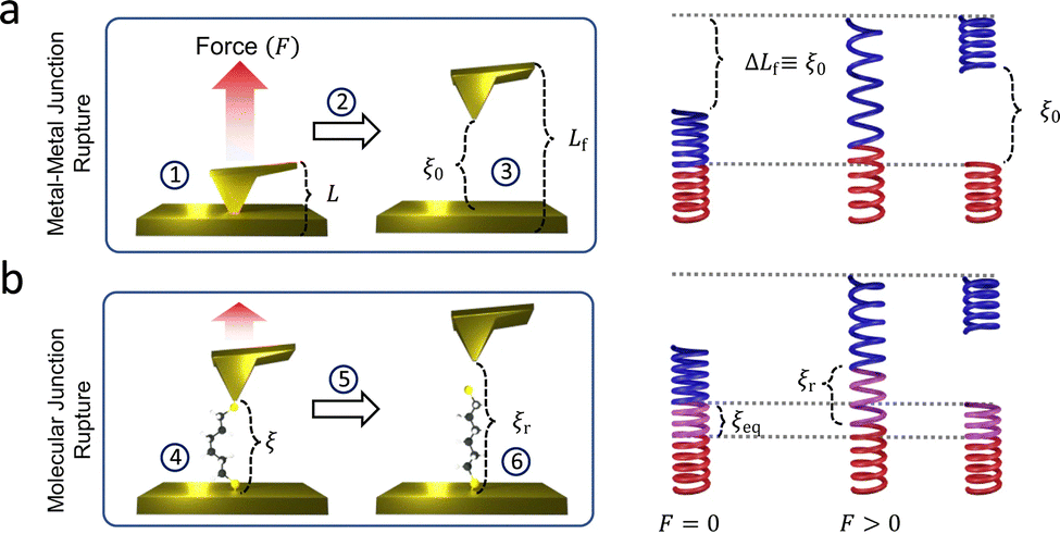 | ||
| Fig. 8 Atomic force microscopy-break junction. The schematic demonstration of the rupture of (a) a metal–metal junction and (b) a molecular junction. Panel is reprinted with the permission from ref. 109, Copyright (2023) Springer Nature. | ||
The ability to resolve single-atom Au conductance plateaus demonstrates the high sensitivity and resolution of AFM-BJ, making it a strong alternative to conventional STM-BJ setups for studying molecular-scale quantum transport. When molecules are bridged between the AFM tip and the substrate, the force required to rupture the junction can confirm molecular connectivity. This rupture force, typically ranging from several hundred piconewtons to a few nanonewtons, provides direct insight into the bond strength between the molecule and electrodes. These values can be extracted through statistical analysis of the force histogram.112–114 By modulating the applied force, the molecular conformation and molecule–electrode bonding configuration can also be characterised.115,116
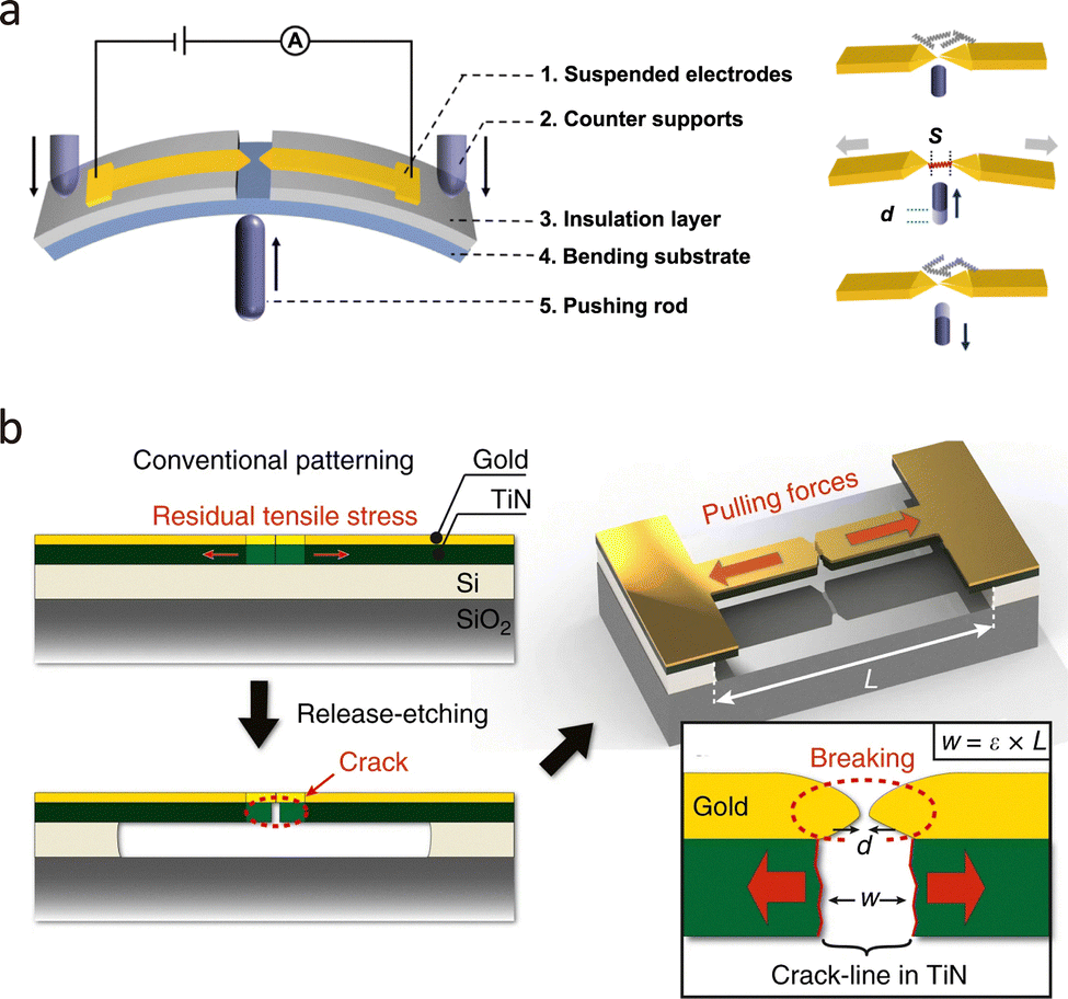 | ||
| Fig. 9 (a) Schematic illustration of MCBJ experimental setup and single molecule detection procedure. (b) Schematic demonstration of the nanogap fabrication through crack-defined break junction. Panel (a) is reprinted with permission from ref. 2, Copyright (2022) by Yi Zhao, under Creative Commons Attribution 3.0 license. Panel is reprinted with permission from ref. 122, Copyright (2018), Springer Nature. | ||
3.3. Passive tunnelling junctions
In biological and soft-matter systems, single molecules typically exist in a freely diffusing state rather than being immobilised. To better simulate these native environments, passive tunnelling junctions have been developed as a label-free platform for investigating molecular processes at the single-entity level.123The concept of passive junctions originates from single-entity electrochemistry at nanoelectrode interfaces. Recent advances in nanofabrication, interfacial chemistry, and time-resolved measurement techniques have enabled researchers to study both soft and hard single entities, including proteins, nanoparticles, and macromolecular assemblies.124 The typical configuration is shown in Fig. 10(a). Unlike conventional fixed-gap junctions, passive molecular junctions are transient tunnelling configurations that form spontaneously during collisions and adsorption between conductive species and an electrode surface, as shown in Fig. 10(b).125 These collisions generate nanogaps typically ranging from 1 to 10 nm, whose width is defined by the molecular length and interfacial interactions. Such configurations permit single- or few-molecule tunnelling events, enabling real-time observation of charge transport and chemical transformations.126
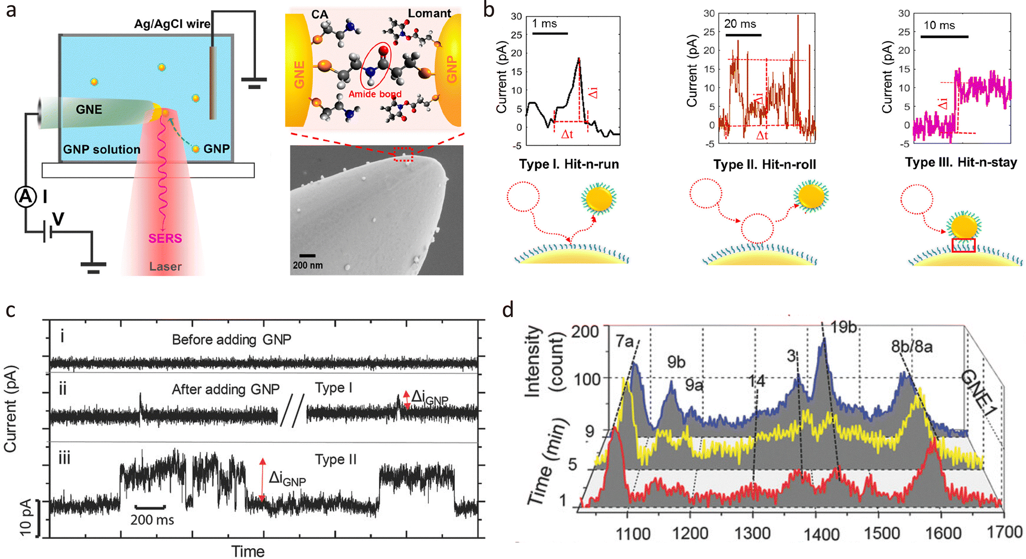 | ||
| Fig. 10 Passive junctions. (a) The schematic demonstrates the experimental setup for SER measurements during the formation of a passive junction. The SEM demonstrates that the Au nanoparticles (GNP) are absorbed on the SAM-modified Au nanoelectrode surface to form a GNP-SAM-GNE collision junction. (b) Three main dynamic behaviours of nanoparticle collision on the GNE and typical current–time response. (c) Real-time current–time traces and (d) SERs response of nanoparticle collision process. Panel (a) and (b) is reprinted with permission from ref. 125, Copyright (2021), American Chemical Society. Panel (c) and (d) is reprinted with permission from ref. 128, Copyright (2018), Wiley-VCH Verlag GmbH & Co. KGaA, Weinheim. | ||
In solution-phase systems, these collisions occur on sub-microsecond timescales, necessitating high temporal-resolution detection. By statistically analysing thousands of individual events, meaningful insights can be extracted despite the stochastic nature of the process.127 Electrical and optical detection methods are commonly employed to monitor passive junctions formation, Fig. 10(c) and (d). For example, collisions between gold nanoparticles and nanoelectrodes produce spike-like or stepwise current responses in I–t trajectories, indicative of discrete tunnelling events.128
Passive junctions also support integration with optical techniques such as surface-enhanced Raman scattering (SERS), which benefits from the intense electromagnetic fields confined within the nanogap. Hybrid optical–electrochemical setups enable the simultaneous probing of redox dynamics, bond formation, and conformational changes with sub-millisecond resolution.129–131 Collectively, passive junctions provide a powerful and flexible approach for investigating molecular recognition, catalytic processes, and reaction mechanisms in complex or biologically relevant environments.
4. Understanding molecular properties through single-molecule conductance measurement
Single-molecule junctions provide a powerful platform to unveil structure–property relationships through single-molecule conductance measurements, thereby informing the rational design and atomic-level assembly of molecular systems. Single-molecule junctions comprise two primary components: the molecular core and the electrode–molecule interface. The molecular core refers to the target molecule that displays distinctive conductance properties, which are heavily influenced by its conformation and electronic state. Meanwhile, the electrode–molecule interface plays a vital role in determining both conductance behaviour and junction stability, shaped by the choice of electrode materials and linker groups.132–134 This section focuses on how molecular structural properties affect single-molecule conductance. We begin by examining the influence of molecular length and structure, then explore the impact of conformational dynamics modulated by external stimuli, and finally highlight recent advances in molecular device design.4.1. Conductance changes in relation to molecular properties
Molecular length is a critical determinant of conductance in single-molecule junctions. When electrons are transported within a molecular junction, depending on whether electrons interact with the molecules, it can be divided into coherent transport (tunnelling) and incoherent transport (hopping). These two transport mechanisms exhibit a competitive relationship. Previous studies have shown that, in two end-anchored single-molecule junctions, as the molecular length increases, electron transport transitions from a direct tunnelling mechanism to a hopping mechanism.21,135,136 In short molecules (1–3 nm), the conductance decreases exponentially with increasing distance, whereas in long-distance cases (3–7 nm), the decay exhibits a linear relationship. However, for molecular junctions that are indirectly connected without anchoring groups, the relationship between conductance and length becomes more complex. Yelin et al.137 demonstrated a systematic investigation of oligoacene (linear π-conjugated molecules) with varying lengths (1–6 benzene rings) using Ag and Pt electrodes, respectively. Due to the lack of linking groups, the π orbitals of oligoacene directly hybridise with the frontier orbitals of metal electrodes, resulting in high conductance. The conductance of Ag/oligoacene junctions initially increases with molecular length before saturating. In contrast, the conductivity of Pt electrodes is close to the conductance quantum and is independent of molecular length. Theoretical analysis suggests that the conductance saturation of Ag electrodes stems from the competition between energy level alignment and energy level broadening, whereas Pt electrodes exhibit band-like transport due to significant π-d hybridisation, resulting in constant conductivity. Similarly, Zhao et al. inserted polycyclic aromatic hydrocarbons (PAHs) of different lengths between graphene electrode pairs and observed the same phenomenon of conductance enhancement.138 However, unlike metal electrodes, the conductance of PAHs on graphene electrode pairs does not show a saturation phenomenon, which is related to the cross-plane charge transport mode of electrons in graphene/PAHs/graphene.Besides conjugated molecules, abnormal conductance–length relationships have also been observed in other types of molecular wires, including those containing metal centres139,140 and Ag nanoclusters.141 This phenomenon is attributed to the narrowing of the HOMO–LUMO energy gap with increasing size, and therefore enhanced coupling between the electrodes and molecules/Ag nanoclusters. Break junction (BJ) techniques enable precise control of nanogap distances from sub-nanometre to sub-10 nm, providing a reliable platform for studying distance-dependent conductance. However, it is important to note that when a molecular bridge spans the electrodes, the measured conductance reflects both direct and molecular tunnelling currents. At very small gaps, leakage currents become significant and must be accounted for.142 The structural characteristics of molecules form the foundation of their chemical and physical properties. Broadly, molecular systems can be divided into conjugated and non-conjugated molecules based on their electron distributions.
In conjugated molecules, the delocalised distribution of electrons enhances the conductivity of molecular junctions, which is often utilised in single-molecule conductance measurements. However, conjugation alone does not fully determine transport properties. Conformational dynamics within the molecule can significantly modulate conductance. For example, in biphenyl derivatives, increasing the torsion angle between the benzene rings leads to a conductance decrease following a cos2θ relationship. Additional rotational degrees of freedom introduce variability, resulting in broader conductance distributions.143 Conversely, restricting conformational freedom yields narrower distributions and well-defined conductance signatures, often independent of nanogap size.144
Rational molecular design offers a powerful means to tune electrical properties. Incorporating substituents or heteroatoms into conjugated backbones alters electron density distribution. The effects depend not only on the nature of the substituents but also on their positional connectivity.145–148 Remarkably, regioisomers with similar chemical structures can exhibit conductance differences spanning several orders of magnitude due to quantum interference effects.149 Embedding metal centres into conjugated wires can modulate the alignment between frontier orbitals and the electrode Fermi level, enhancing conductance.139,140 Another crucial factor is the anchoring group, which governs the coupling strength and binding geometry at the electrode–molecule interface. Systematic studies have shown that both the type and position of anchoring groups influence transport pathways and junction stability.150–153 Importantly, structure–property relationships in molecular junctions cannot be reduced to a single parameter. Instead, they emerge from the cooperative interplay of multiple structural features, including molecular length, conformation, substituent effects, and interface chemistry.
In addition to one-dimensional (1D) molecular wires, conductive molecules with more complex architectures, such as topological structures and supramolecular assemblies, have increasingly attracted research interests. For example, Stuyver et al. theoretically examined the topological transformation of conjugated porphyrin molecules and demonstrated efficient conductance switching. Molecular devices with switch ratios of up to three orders of magnitude can thus be designed.154 Ganna et al. reported that saturated carbon nanowires (such as polytwistane) exhibited conductivity with six orders of magnitude higher than that of 1D linear alkane chains of the same length, achieved through topological structure design.155 Conductance decays slowly with increasing nanogap size, with a β value of only 0.55 nm−1. These findings suggest new strategies for designing highly conductive single-molecule junctions, indicating that even in systems lacking π conjugation, optimisation of topological structure can markedly enhance conductivity. For the supramolecular structure, the electrical transport properties of supramolecular junctions based on hydrogen bonds,156 π–π stacking,157 σ–σ stacking,158 and host–guest159 interactions have also been characterised and reported. Although research into supramolecular junction conductance has spanned over a decade, the exploration of complex biomolecular systems based on these interactions remains in its early stages. Establishing robust structure–property relationships in supramolecular systems remains a dynamic and evolving field of investigation.
4.2. Monitoring conformation changes at the single-molecule scale
Molecular conformational dynamics are susceptible to environmental conditions and external stimuli, such as electric fields, mechanical forces, and optical irradiation. Traditional ensemble-averaged techniques offer insights into bulk behaviour but mask molecular heterogeneity and transient intermediates. In contrast, single-molecule conductance measurements provide real-time, high-resolution access to molecular geometry, electronic structure, isomerisation, enantiomer discrimination, and intermolecular interactions. This capability has broad implications for catalysis, drug discovery, molecular electronics, and biophysics. Here, we review recent advances in single-molecule conductance platforms for probing stimulus-induced structural transitions, including liquid modulation, electric fields, mechanical stretching, and optical excitation.In liquid regulation of the electrical properties of molecular junctions, the proton-transfer process has been demonstrated as a simple and efficient method for constructing bistable molecular structures, exhibiting extremely high response sensitivity in conductance measurements. Proton transfer can be reversibly controlled by adjusting the solution pH. For example, proton transfer has been demonstrated to be an effective method for regulating quantum interference in molecular junctions, thereby influencing molecular conductance. As shown in Fig. 11(a), Zhang et al. employed the MCBJ technique to measure the single-molecule conductance of two DPP derivatives (SDPP and SPPO) at room temperature.160 The single-molecule conductance of two DPP isomers was identical in a mixed chloroform/mesitylene solution. The responses of the two isomers to protonation regulation in the solution show significant differences, enabling them to be effectively identified. As shown in Fig. 11(b), both experimental and theoretical results indicate that the protonated SPPO molecule exhibits a cross-conjugated structure, which can trigger a destructive quantum interference, thereby suppressing electron transport and leading to a significant reduction in conductance. In contrast, the unprotonated SPPO molecule exhibits a linear conjugated structure, facilitating electron transport and resulting in a higher conductance. Moreover, Tang et al. reported the reversible switching between destructive and constructive quantum interference (QI) in single-molecule junctions via H+ or Me+ atomically precise chemical gating.161 The protonation or methylation led to the interchange of frontier orbitals, switching the QI pattern and causing significant modulation of conductance.
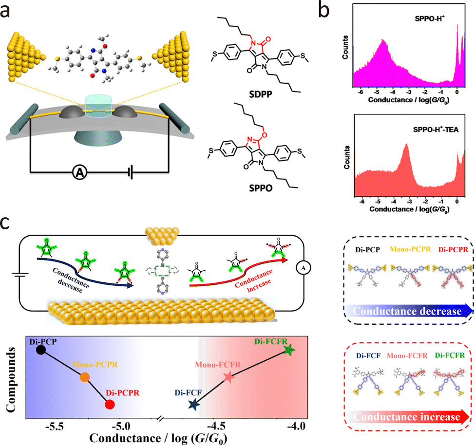 | ||
| Fig. 11 (a) Schematic illustration of DPP junctions created by the MCBJ platform and the corresponding molecular structures of DPP isomers. (b) Conductance histograms of SPPO-H+ junctions and SPPO-H+-TEA junctions showing reduced conductance values for protonated SPPO. (c) Schematic diagrams of the progression of single-molecule conductance for PCP and FCF junctions with radical injection. Panels (a) and (b) are reprinted with the permission from ref. 160, Copyright (2018), American Chemical Society. Panel (c) is reprinted with the permission from ref. 163, Copyright (2024) by Hanjun Zhang, under CC BY-NC 4.0 license. | ||
In organic molecules, the injection of radicals can profoundly influence charge distribution and molecular structure. From a single-molecule perspective, radicals, due to their unique electronic characteristics, can significantly modulate the electrical transport properties of molecular junctions. Their presence in solution introduces dynamic charge perturbations that interact with the molecular backbone and electrode interfaces, making radical injection a highly promising strategy for tuning conductance at the nanoscale. This approach opens new avenues for the design of molecular wires with enhanced electrical conductivity.162 Recently, Zhang et al. demonstrated bidirectional conductance modulation in single-molecule junctions through off-site radical injection.163 As shown in Fig. 11(c), applying cyclopentadienone derivatives with distinct conjugation pathways (cross-conjugated PCP vs. linearly conjugated FCF), they revealed that radical injection decreases conductance in PCP systems (Mono-PCPR: 10−5.37G0, Di-PCPR: 10−5.85G0) due to destructive quantum interference, while increasing conductance in FCF systems (Mono-FCFR: 10−4.22G0, Di-FCFR: 10−3.97G0) via through-bond enhancement, which was further confirmed by flicker noise analysis and theoretical calculations.
Molecules possess intrinsic dipole moments arising from the spatial distribution of positive and negative charges. The application of an electric field exerts force on these internal charges, influencing molecular orientation, charge distribution, and motion state.147,165 By designing molecules with tailored dipole moments, their electrical properties can be actively modulated under field stimuli. In 2016, Harzmann et al. reported a single-molecule spin switch based on the voltage-induced distortion of the coordination sphere of FeII species.166 By designing heteroleptic [FeII(tpy)2] complexes with one tpy ligand anchored in the junction and the other exhibiting a dipole moment sensitive to electric fields, the researchers demonstrated that the spin state of FeII can be altered through electric field-triggered distortion of its coordination sphere. According to Fig. 12(a), statistical analysis of a large number of junctions revealed that the proportion of junctions exhibiting voltage-dependent bistability increases with the dipole moment of the FeII complexes, while the threshold electric field required for switching remains constant, further supporting the proposed switching mechanism. This work not only provides a new strategy for controlling spin states in molecular electronics but also paves the way for the development of high-performance, reversible single-molecule spintronic devices.
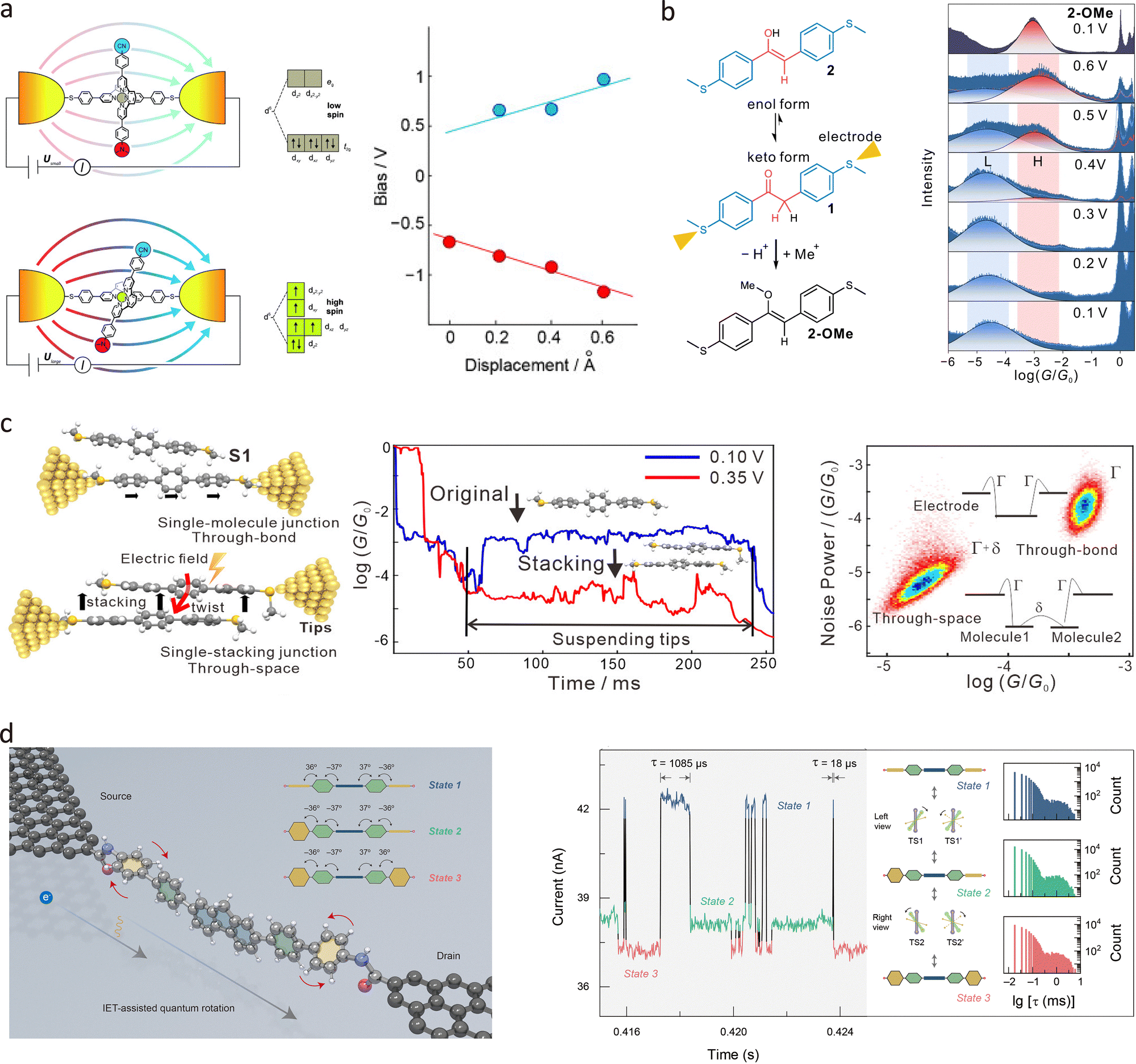 | ||
| Fig. 12 (a) Schematic diagrams of the voltage-induced single-molecule spin switch, demonstrating the dominant role of the ligand's dipole moment in the spin switching process. Right panel: The evolution of the bistable transition voltage with electrode spacing shows that the electric field threshold remains constant. (b) Molecular structure of the compound with the enol tautomeric unit as the centre and its keto isomer. Right panel: 1D conductance histograms of the keto compound across biases from 0.1 to 0.6 V, revealing a voltage-induced shift from low-conductance (L) to high-conductance (H) states. (c) Schematic illustration of the single-terphenyl junction and the terphenyl-stacking junction. Typical conductance traces of terphenyl junctions at 0.10 V and 0.35 V indicate conductance changes during stretching. A 2D histogram of noise power versus average conductance highlights differences in noise characteristics between the single-terphenyl junction and the terphenyl-stacking junction. (d) Schematic illustration of the single-molecule junction with a hexaphenyl aromatic molecule covalently embedded in graphene electrodes, illustrating the quantum rotation effect. The typical I–t curve and dwell times of three states suggest two conversion pathways with different rates. Panel (a) is reprinted with permission from ref. 166, Copyright (2015), Wiley-VCH Verlag GmbH & Co. KGaA, Weinheim. Panel (b) is reprinted with permission from ref. 167, Copyright (2023), Springer Nature. Panel (c) is reprinted with permission from ref. 168, Copyright (2020), American Chemical Society. Panel (d) is reprinted with permission from ref. 169, Copyright by Yilin Guo (2025), under CC BY-NC 4.0 license. | ||
Tautomerisation, the interconversion of structurally similar isomers, is another key focus in conformational studies. In non-degenerate systems, a single tautomer typically dominates at thermodynamic equilibrium, limiting reversible switching. Electric field modulation offers an alternative strategy for controlling tautomerisation at the single-molecule level. Tang et al.167 developed a strategy for controlling the keto–enol equilibrium of a single molecule within a two-terminal junction system through voltage modulation at room temperature. The researchers designed a molecular component with a keto–enol tautomeric unit positioned between two thioanisole anchors, allowing the charge transport pathway to pass through the tautomeric unit. Using the STM-BJ technique shown in Fig. 12(b), they found that the conductance of the molecular junction could be significantly modulated by altering the applied voltage. At a low bias of 0.1 V, the junction predominantly existed in the low-conductance keto form, while at a higher bias of 0.6 V, it transitioned to the high-conductance enol form, with a conductance increase of approximately 67 times. The electric field not only reduces the keto–enol tautomerisation barrier but also alters the thermodynamic driving force, making the enol form thermodynamically stable in the charged state.
Electric fields also play a critical role in modulating intermolecular interactions. In 2020, Tang et al. investigated electric field-induced molecular stacking in single-stacking terphenyl junctions using the STM-BJ technique.168 As demonstrated in Fig. 12(c), the formation of stacking junctions between two terphenyl molecules increases with the intensity of the applied electric field. The conductance measurements showed a high-conductance peak at 0.10 V (blue), which increased further at 0.35 V (red), followed by a more pronounced low-conductance peak. These conductance plateaus change with voltage because the dihedral angles between adjacent phenyl rings decrease under an electric field, making the molecules more planar and promoting energetically favourable molecular stacking configurations. A 2D histogram of noise power versus average conductance from simulated data, highlights the distinct noise characteristics of intramolecular and intermolecular transport.
Recently, Guo et al. prepared a fluorene-centred hexaphenyl aromatic molecule and integrated it into a graphene electrode pair via covalent bonds.169 As shown in Fig. 12(d), current–time measurements at 120 K revealed three discrete metastable states, attributed to varying degrees of conjugation between the terphenyl segments. The dynamic rotation of phenyl rings at low temperatures was governed by quantum rotational tunnelling rather than quasi-free rotation. Crucially, the electric field influenced both the direction and energy of rotation, enabling more complex rotational modes as the bias voltage increased.
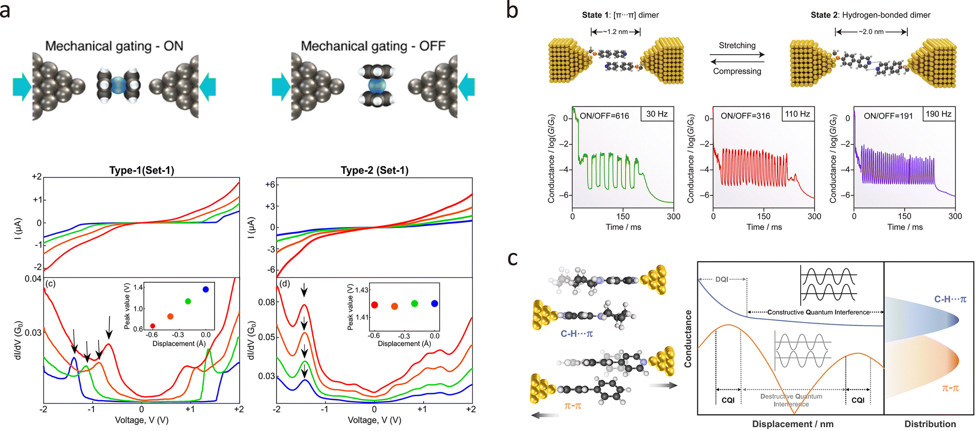
In 2023, Pabi et al. proposed that the mechanical gating of molecular junctions is significantly influenced by the molecular orientation within the junction.177 They found that silver–ferrocene–silver junctions can exhibit either clear mechanical gating (type 1) or non-mechanical gating (type 2), depending on the molecular orientation. As shown in Fig. 13(a), altering the interelectrode distance results in a clear mechanical gating effect in type 1 junctions, with reduced separation shifting molecular energy levels closer to the Fermi level, thereby enhancing conductance. However, type 2 junctions showed no significant change in their conductance spectra upon similar mechanical manipulation. DFT calculations revealed that the molecular junction could adopt two configurations: parallel and perpendicular to the electrode axis. In the parallel configuration, mechanical squeezing rigidly shifted the transmission characteristics to lower energies, increasing conductance. Conversely, in the perpendicular configuration, no significant shift in transmission peaks was observed. These findings underline the critical role of molecular orientation in determining mechanical gating efficiency, introducing a new degree of freedom for tuning mechanically responsive molecular junctions.
 | ||
| Fig. 13 (a) Schematic illustration of silver–ferrocene–silver junctions with mechanical gating behaviour. Current–voltage characteristics of Ag–ferrocene–Ag junctions (type 1/type 2) showing mechanical modulation of molecular orbit alignment and conductance via interelectrode distance variation. (b) Schematic illustration of the switch between the [π⋯π] and hydrogen-bonded dimer junctions. The 2D and 1D conductance histograms of designed supramolecular junctions showing the piezo-modulated switching. (c) Schematic illustration of conductance evolution through π–π and C–H⋯π interactions with displacement. Panel (a) is reprinted with permission from ref. 177, Copyright by Biswajit Pabi (2023), under CC-BY 4.0 license. Panel (b) is reprinted with permission from ref. 166, Copyright (2023), American Chemical Society. Panel (c) is reprinted with permission from ref. 179, Copyright (2024), American Chemical Society. | ||
Mechanical force has also proven effective in probing intermolecular interactions. By stretching or compressing the junction, researchers can modulate the degree of stacking of conjugated molecules, alter charge-transport pathways in supramolecular assemblies, and even observe quantum-interference oscillations. Recently, Zhou et al. constructed robust single-supermolecule switches by harnessing two different non-covalent interactions between pyridine derivatives.178Fig. 13(b) demonstrated that the conductance is high when the phenylene-pyridine backbone forms face-to-face [π⋯π]-stacked dimers upon junction compression. In contrast, upon junction stretching, the formation of double [C–H⋯N] hydrogen bonds between neighbouring pyridine units leads to a significant decrease in conductance. These switches operated reliably at frequencies up to 190 Hz, demonstrating excellent reproducibility. Additionally, Zhou et al. investigated the charge transport properties of supramolecular junctions formed by C–H⋯π and π–π interactions, as shown in Fig. 13(c).179 Their findings revealed that C–H⋯π interactions enable more efficient charge transport than π–π stacking, with conductance measurements showing C–H⋯π junctions exhibit approximately 350% higher conductance. The study also revealed that the conductance of C–H⋯π junctions initially decreases with stretching and then gradually stabilises, unlike the periodic fluctuations observed in π–π stacked junctions. Theoretical analysis attributed this behaviour to a transition from destructive to constructive quantum interference in C–H⋯π interactions as the junction is stretched.
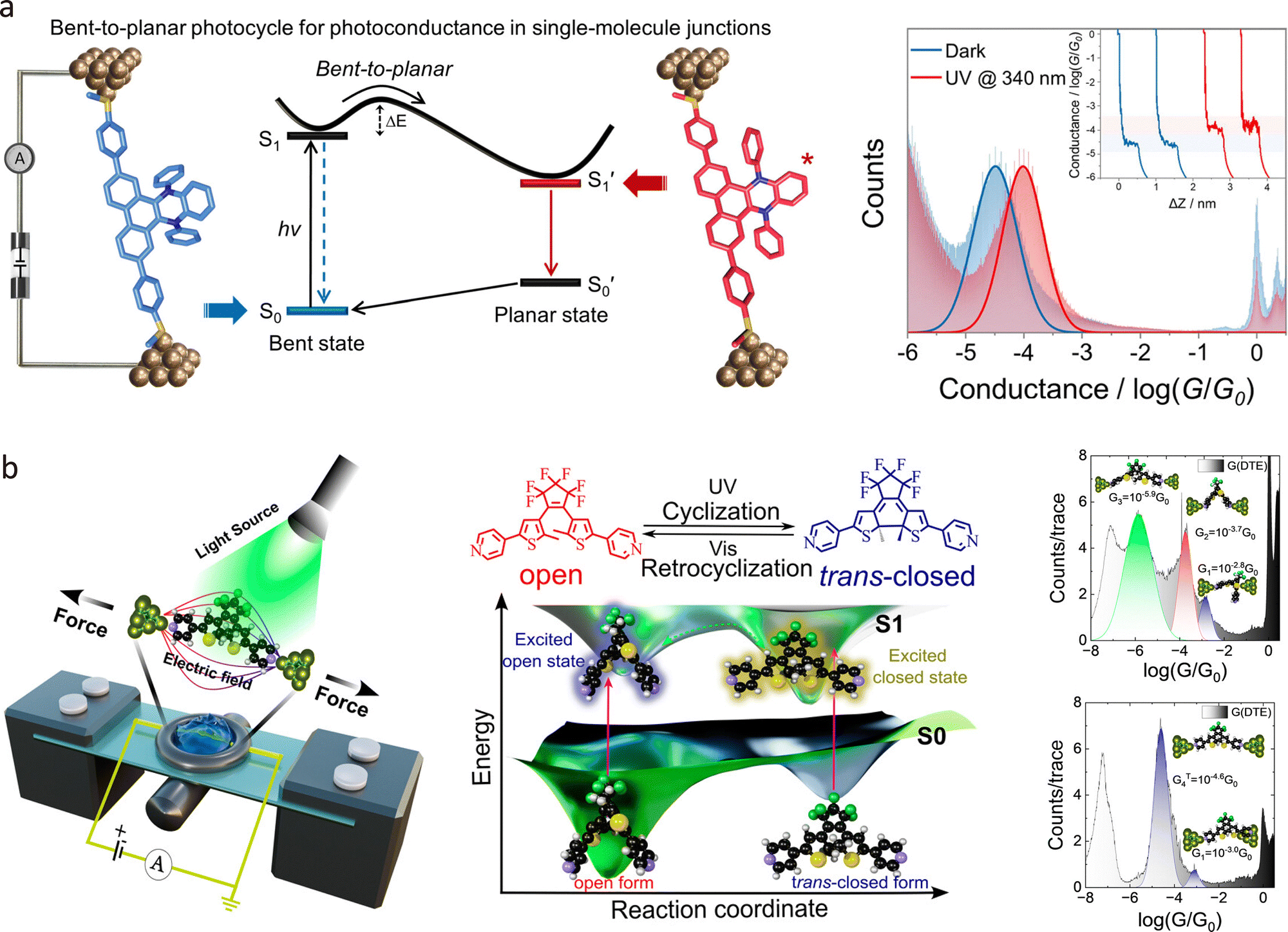
In 2022, Zou et al. employed the STM-BJ technique to fabricate single-molecule junctions of 9,14-diphenyl-9,14-dihydrodibenzo[a,c]phenazine (DPAC), enabling exploration of the photoconductance dependence on excited-state structural and electronic changes.182 As shown in Fig. 14(a), the π-delocalisation of DPAC-SMe junctions showed a distinguished and reversible photoconductance of up to ∼200% under continuous 340 nm light irradiation. This enhancement was attributed to a photoinduced bent-to-planar conformational transition in the excited state, which significantly altered the electron density distribution and gave rise to Fano resonance. Additionally, in situ conductance modulation was observed under pulsed irradiation at 340 nm, further confirming the dynamic nature of the photoresponse. Femtosecond transient absorption (TA) spectroscopy revealed an isomerisation process in the excited state, with two distinct local minima in the S1 state. The TA spectra showed a strong absorption band at 1160 nm, which reached a maximum within 5 ps and then decayed, indicating the formation of a fast bent state.
 | ||
| Fig. 14 (a) Schematic illustration of the bent-to-planar photocycle process of the DPAC-SMe junctions. Right panel: The 1D conductance histogram shows the single-molecule conductance of DPAC-SMe junctions enhanced upon light irradiation. (b) Schematic illustration of the DTE junction under multi-mode external stimuli and corresponding photoisomerisation processes. Roight panel: 1D conductance histograms show various conductance states of DTE junctions for the “open” and “trans-closed” forms, indicating an isomer trapped within the molecular junction undergoes transformation to another isomer during junction evolution. Panel (a) is reprinted with permission from ref. 182, Copyright (2022), American Chemical Society. Panel (b) is reprinted with permission from ref. 183, Copyright (2025), American Chemical Society. | ||
Recently, Rashid et al. demonstrated that isomerisation in photoswitchable molecules can be triggered by mechanical force and oriented electric fields, thereby bypassing the need for excited-state configurations.183 As shown in Fig. 14(b), the ground-state reactivity of a dithienylethene (DTE) derivative was explored using MCBJ techniques, revealing that external perturbations can control reaction dynamics and steer reaction trajectories away from typical excited-state pathways. The study identified distinct conductance states corresponding to different isomeric forms of the DTE molecule and showed that mechanical force could induce isomerisation in the absence of light. Additionally, the researchers mapped an extended ground-state potential energy surface for the DTE derivative, highlighting the ability to stabilise intermediates and metastable states along the reaction pathway. This work provides a strategy for probing and stabilising different intermediates and metastable states in photochromic systems, enabling the production of desired stereoselective products without conventional photonic stimuli.
When a metal nanogap is illuminated at its resonance wavelength, it can excite the localised surface plasmon resonance (LSPR), resulting in enhanced local electromagnetic fields, the generation of hot carriers, and localised thermal effects. Depending on different phenomena, various effects can be produced on the structure and properties of molecular junctions. Recently, it has been shown that the electromagnetic field enhancement induced by LSPR can be utilised to generate optical gradient forces within tunnelling junctions, thereby capturing molecules in the vicinity of the nanogap, enabling single-molecule plasmonic optical tweezers.184,185 Very recently, Xu et al. investigated the π–π interactions between single molecules using the STM-BJ technique.186 As shown in Fig. 15(a), they employed 2,6-naphthalenediamine (2,6-NA) molecules, which have two amino anchoring groups and naphthalene as the backbone to form π–π stacking dimers. Conductance measurements of thousands of single-molecule junctions revealed distinct peaks in 1D and 2D conductance histograms, corresponding to molecular monomer and dimer junctions. Under laser illumination (λ = 532 nm, intensity ∼1 × 10⁴ Wm−2), the low-conductance peak, attributed to dimer junctions, exhibited a significant rightward shift and intensity increase, while the high-conductance peak remained largely unchanged. This indicated enhanced π–π coupling between molecules under light. Furthermore, flicker noise analysis was performed, demonstrating that the flicker noise power-scaling factor decreased upon illumination, supporting the enhanced π–π coupling. Analysis based on finite-element and a quasi-quantum method revealed that the enhanced π–π interaction originated from the optical gradient force within the nanogaps. This study provides a non-destructive method for regulating π–π interactions at the single-molecule level.
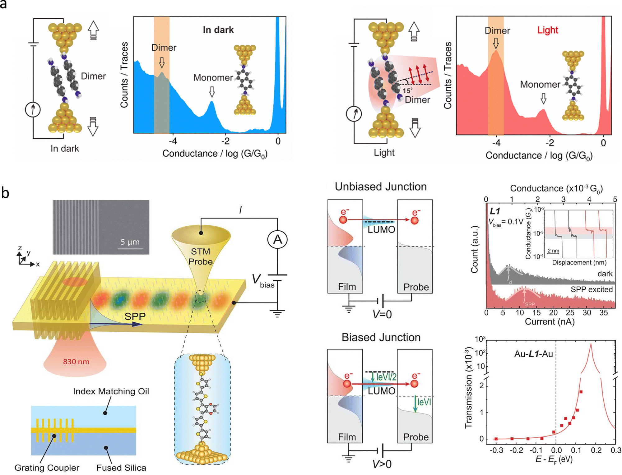 | ||
| Fig. 15 (a) Schematic illustration of π-stacked 2,6-NDA junctions and corresponding 1D conductance histograms under dark-illumination conditions, showing enhancement of formation probabilities for low conductance states assigned to the π-stacked dimer junctions. (b) Schematic illustration of experimental setup for HCEDs mapping. Middle panel: schematic illustrating the hot carrier's generation and transport process in the LUMO-determined single-molecule junction. Right panel: current histograms for the LUMO-determined single-molecule junction with and without SPP excitation, and the corresponding measured transmission functions with Lorentzian fit. Panel (a) is reprinted with permission from ref. 186, Copyright (2024), American Physical Society. Panel (b) is reprinted with permission from ref. 190, Copyright (2020), American Association for the Advancement of Science. | ||
The plasmon-enhanced single-molecule conductance depends on the coupling between the optical field and the molecular junctions. Under the excitation of the plasmonic optical field, on one hand, an instantaneous alternating electric field at the optical frequency can be generated in the nanoscale gap, inducing an alternating current that is rectified into a direct current within the nanoscale gap structure,187 thereby enhancing the conductance of the molecular junction.188 On the other hand, the hot electrons generated by the LSPR effect are driven by the electric field and injected into the molecular junction, significantly enhancing the photoconductance of the molecular junction.189 However, the roles of these two mechanisms in plasmon-enhanced single-molecule conductance remain vague and require more refined experimental designs for further study. A remarkable advancement was reported by Reddy et al. on an indirect optical field coupling method to quantify plasmonic hot-carrier energy distributions (HCEDs) using single-molecule transport measurements.190 As shown in Fig. 15(b), by forming single-molecule junctions between an ultrathin gold film supporting surface plasmon polaritons and a scanning probe tip, they measured the current–voltage characteristics with and without plasmonic excitation. The difference in currents, termed the hot-carrier current (Ihot), allowed them to quantify HCEDs directly. In detail, the HCEDs in gold films with thicknesses of 6 nm and 13 nm were mapped, showing a 40% reduction in the total number of hot carriers in the 13-nm-thick films, supporting the mechanism of Landau-damping-dominated hot-carrier generation. This work provides insights into hot-carrier generation at the single-molecule level, offering a foundation for engineering technologies that harness plasmonic hot carriers.
Another emerging research direction in single-molecule optoelectronics is to couple ultrafast light with molecular junctions, thereby obtaining high spatiotemporal-resolution information through electrical measurements. In 2016, Cocker et al. proposed tracking the ultrafast motion of a single pentacene molecule using femtosecond orbital imaging with THz-STM.191 The team demonstrated selective tunnelling through the HOMO of a pentacene molecule within a sub-cycle time window, removing a single electron in approximately 100 femtoseconds. Furthermore, they revealed coherent molecular vibrations at terahertz frequencies via pump/probe measurements. This work enabled the visualisation of ultrafast photochemical processes and molecular electronics at the single-orbital level, offering insights into molecular electronic and vibronic dynamics with atomic precision and ultrafast temporal resolution.192,193
Moreover, the introduction of ultrafast lasers provides a means for manipulating and controlling individual molecules. In 2020, Peller et al. demonstrated the coherent control of a single-molecule switch using ultrafast atomic-scale forces.194 As shown in Fig. 16(a), the researchers utilised a terahertz wave confined to an atomically sharp tip to induce femtosecond forces that selectively drive coherent hindered rotation in a bistable magnesium phthalocyanine molecule. The study revealed that these ultrafast forces can modulate the probability of the molecule switching between its two stable adsorption geometries by up to 39%. The findings highlight the potential for ultrafast structural transitions in quantum systems, paving the way for sub-cycle atomic-scale control of chemical reactions and phase transitions. Recently, Liu et al. developed a single-molecule photoelectron tunnelling spectroscopy technique that maps transmission beyond the HOMO–LUMO gap of a diketopyrrolopyrrole (DPP) molecule junction at room temperature by integrating ultrafast laser pulses with the STM-BJ setup shown in Fig. 16(c).195 This method unveiled two resonant transport channels at 1.45 eV and 1.70 eV, corresponding to the LUMO+1 and LUMO+2 orbitals of DPP junctions, as confirmed by density functional theory calculations.
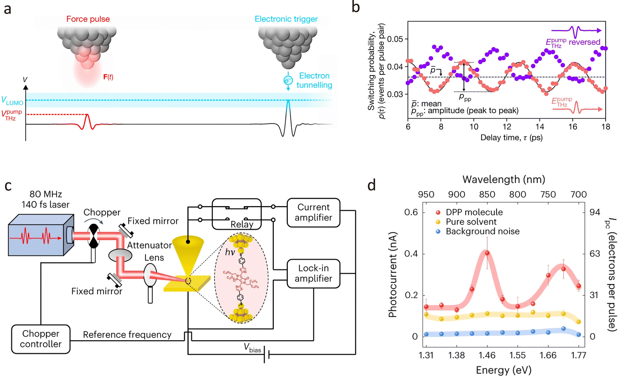 | ||
| Fig. 16 (a) Schematic diagram of coherent control of a single-molecule switch using THz pump–probe pulse pairs. (b) The switching probability of a single-molecule switch as a function of delay time between pump and probe pulses, showing a pronounced oscillation at a frequency of 0.3 THz. (c) Schematic illustration of the single-molecule photoelectron tunnelling spectroscopy setup. (d) The experimental maps of the transmission function of the DPP junction by photocurrent spectrum. Panels (a) and (b) are reprinted with permission from ref. 194, Copyright (2020), Springer Nature. Panels (c) and (d) are reprinted with permission from ref. 195, Copyright (2023), Springer Nature. | ||
4.3. Single-molecule electronic devices
Research into structure–property relationships at the single-molecule level not only deepens our fundamental understanding of physicochemical behaviour at the molecular scale but also enables the identification and optimisation of functional molecules for constructing molecular electronic devices capable of logic operations. Since the conceptual proposal of single-molecule rectifiers, a diverse array of functionally designed molecular devices has been demonstrated, including molecular switches,196 molecular rectifiers,197 molecular diodes,198 molecular transistors,199 and molecular memory.200 The integration of external stimuli-responsive modulation has introduced configurational flexibility into molecular device design, significantly enhancing performance. Moreover, quantum interference effects have emerged as a powerful mechanism for modulating electronic behaviour, enabling on/off ratios spanning several orders of magnitude and offering exceptional control over conductance.In 2023, Li et al. reported the fabrication of supramolecular transistors based on π-stacked thiophene/phenylene co-oligomers (TPCOs) with controllable quantum interference effects.201Fig. 17(a) demonstrates the experimental setup of the electrochemically gated scanning tunnelling microscope break junction (EC-STM-BJ) technique. They achieved precise control over the configuration of the supramolecular channels, resulting in a transistor with an on/off ratio of approximately 1300, a gating efficiency of 165 mV dec−1, and an off-state leakage current of about 30 pA, with a channel length scaled to <2.0 nm. This work highlights the potential of supramolecular architectures as channel materials for sub-2 nm molecular transistors, providing insights into configuration-dependent charge transport mechanisms. The ability to fine-tune quantum interference features through the design of molecular architecture opens new avenues for the development of high-performance molecular electronic devices. In Fig. 17(b), Guo et al. presented a single-molecule diode achieving an exceptional rectification ratio of up to 5000 and effective AC-to-DC conversion.202 This was achieved via electric-field-catalysed Fries rearrangement, which toggled between constructive and destructive quantum interference states. The diode demonstrated stable operation across nearly 100 devices and was successfully integrated into on-chip half-wave and full-wave rectifier circuits.
 | ||
| Fig. 17 (a) Schematic illustration of the supramolecular transistor and corresponding molecular structures employed for forming the π–π stacked junctions. The field-effect response of the supramolecular transistor at an electrode potential from −0.2 to 0.8 V, showing an on/off ratio of approximately 1300. (b) Schematic illustration of the operation of the graphene-based single-molecule diode with the phenyl benzoate functional centre. The comparison of rectified radio values of the different single-molecule diode devices in Lewis-acidity-dependent measurements. (c) Schematic illustration of the single-metallofullerene memory device and corresponding mechanisms for logic-in-memory operations at room temperature. (d) Schematic illustration of a graphene-based single-molecule optoelectronic device with a heavy atom centre (Pt) for real-time communication via programmable voltage pulses, which trigger the selective emission of phosphorescence and fluorescence. Panel (a) is reprinted with permission from ref. 201, Copyright (2023), American Chemical Society. Panel (b) is reprinted with permission from ref. 202, Copyright (2025), American Chemical Society. Panel (c) is reprinted with permission from ref. 203, Copyright (2022), Springer Nature. Panel (d) is reprinted with permission from ref. 204, Copyright (2024), Elsevier. | ||
Although the performance of single-molecule devices is being progressively optimised and approaching that of conventional electronics, they face a critical bottleneck in achieving multi-device integration. To address this, researchers have begun exploring logic operations using individual molecular devices. In 2022, Li et al. demonstrated room-temperature logic-in-memory operations in single-metallofullerene devices.203 As shown in Fig. 17(c), by manipulating the independent permanent dipole of [Sc2C2] within the fullerene cage using pulsed bias voltages, reversible encoding and storage of digital information were achieved. The devices exhibited non-volatile memory behaviour with a conductance switching ratio of up to 500%, and successfully implemented 14 types of Boolean logic operations. Very recently, Yang et al. reported a graphene-based single-molecule optoelectronic device featuring a platinum (Pt)-centred molecular bridge encapsulated by two cyclodextrins (CDs) (Pt-MB@CD).204 This design, shown in Fig. 17(d), effectively isolates the molecule from environmental interactions, dramatically enhancing device performance. A high quantum yield (∼106) and an ultra-long phosphorescence lifetime (millisecond-scale) were achieved at the Pt-centred single-molecule junction. Employing single-molecule transient electroluminescence spectroscopy (sm-TES), they directly observed and manipulated the molecule's tuneable singlet and triplet excited states via multimodal electrical inputs. This precise control over fluorescence and phosphorescence, enabling selective emission, allowed the single-molecule device to perform comprehensive binary and trinary logical operations. Moreover, the device successfully demonstrated real-time communication capabilities by programming electrical pulses (10-ms intervals, 1-ms width) to tune molecular excited states. Photon energy and timing encode binary streams (e.g., ASCII), facilitating the display of 1D/2D data (e.g., a university logo). This study realises a highly integrated, high-performance, multifunctional, and stable single-molecule optoelectronic device on a chip, representing a significant step towards bridging the conceptual gap between molecular electronics and practical semiconductor applications.
In addition to exploring individual molecules as candidates for molecular electronics, self-assembled monolayers (SAMs) spanning two electrodes provide a pathway for constructing molecular ensemble junctions. By systematically tuning molecular length, functional groups, anchoring chemistry, and electrode materials, these junction arrays can be engineered with well-defined electronic properties. Such highly integrated platforms demonstrate significant potential for on-chip device fabrication and even offer opportunities for incorporation into semiconductor technologies.205,206
For instance, the position of the functional group within the molecular backbone has been shown to determine rectification behaviour. As shown in Fig. 18(a), Nijhuis et al. demonstrated that shifting the location of a ferrocene moiety along an alkanethiol chain systematically tuned its coupling to the electrodes, even reversing the direction of rectification in SAM-based diodes. The position of the ferrocene molecule between the AgTS-SCnFcC13−n//Ga2O3/EGaIn can optimise the frontier orbital alignment and charge transport, which leads to a different rectification direction.207 The anchoring or terminal group is another important factor influencing conductivity. As shown in Fig. 18(b), systematic studies demonstrated that varying halogen terminations in HS(CH2)nX SAMs with GaOx/EGaIn top contacts produced pronounced differences in tunnelling decay constants (β). Substitution with iodine (X = I) enhanced current densities by more than four orders of magnitude, accompanied by an increased dielectric constant (εr), a reduced HOMO–LUMO gap, and lower contact resistance. Such findings emphasise that the selection of the anchoring group interferes with the efficiency of electron transport.208 Moreover, the electrode material itself also exerts a strong influence on the conductance. As shown in Fig. 18(c), Han et al. reported that junctions formed on Ag, Au, and Pt displayed markedly different rectification directions, a consequence of Fermi level pinning and variable charge transfer at the metal–molecule interface.209 This finding demonstrated that electrode identity can be as important as molecular design in defining device function.210 Beyond these static parameters, the incorporation of stimuli-responsive functional groups introduces an additional level of control, enabling active modulation of charge transport within SAM-based junctions. In Fig. 18(d), Cao et al. applied azobenzene-based SAMs to construct dynamic molecular switches and demonstrated reversible conductance modulation via light-driven cis–trans isomerisation. Optimisation of the molecule–electrode coupling enabled reproducible transitions between high- and low-conductance states, providing a proof-of-concept for switchable SAM-based junctions.211
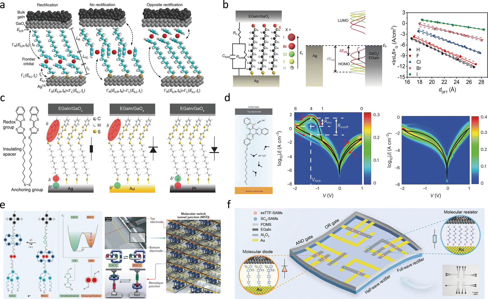 | ||
| Fig. 18 (a) The schematic illustration of the position of the Fc molecule in AgTS-SCnFcC13−n//Ga2O3/EGaIn junction leads to the different rectification functions. (b) The schematic illustration the anchoring group at Ag–S(CH2)nX//GaOx/EGaIn junction, along with the energy level diagram of the halogen atom. The corresponding decay plots of 〈log10|J|〉Gversus dDFTA at −0.5 V demonstrate that halogen atom at GaOx/EGaIn leads to different conductance. (c) The schematic illustration of the substrate material and corresponding electric properties of the M–S(CH2)11S–BTTF//GaOx/EGaIn junctions. The Ag substrate is prone to non-rectification, whereas the Au and Pt substrates exhibit rectification in opposite directions. (d) Schematic illustration (left) and corresponding log10|J| versus V plot in relative humidity = 60% in ambient conditions (middle) and 10 ppm water (right). (e) (left) Schematic illustration of the structure and corresponding energy diagram of the amphiphilic bistable [2] rotaxane R4+ in its ground-state co-conformation (GSCC) and metastable co-conformation (MSCC). (Right) A MIM-based dynamic random-access memory circuit and integration of MSTJ into crossbar devices. The memory effect is caused by the conductance switching between GSCC and MSCC. (f) Schematic illustration of the flexible molecular device with integrated circuits to realise both logic gates and rectifiers. Panel (a) is adapted from ref. 207, Copyright (2015), Springer Nature. Panel (b) is adapted from ref. 208, Copyright (2021) by Xiaoping Chen, under Creative Commons Attribution 4.0 International License. Panel (c) is adapted from ref. 209, Copyright (2021) by Ziyu Zhang, under CC-BY-NC-ND 4.0 License. Panel (d) is adapted from ref. 211, Copyright (2022) by Yulong Wang, under exclusive licence to Springer Nature Limited. Panel (e) is adapted from ref. 212, Copyright (2021), Springer Nature. Panel (f) is adapted from ref. 215, Copyright (2024), Wiley-VCH GmbH. | ||
Beyond single molecules, supramolecular systems can also serve as the functional components of SAM-based junctions, as demonstrated in Fig. 18(e).212 In 2006, Stoddart et al. reported that bistable [2] rotaxanes could be integrated into monolayer junctions and operated as switchable elements, where redox-driven translational motion of the ring along the dumbbell backbone directly modulated tunnelling conductance.213 This concept was later advanced into large-area crossbar memory devices, in which rotaxane monolayers sandwiched between orthogonal nanowire arrays functioned as individually addressable memory cells. With densities approaching 1011 bits cm−2, these systems demonstrated the feasibility of defect-tolerant supramolecular memories and established mechanically interlocked molecules as versatile candidates for molecular-scale information storage.214
Moreover, integrating multiple SAM layers on a single chip provides a compelling demonstration of how molecular junctions can be functionalised for multiple purposes. In Fig. 18(f), Li et al. reported a unique crossbar architecture using EGaIn–molecule–Au junctions. In this system, alkanethiol monolayers acted as molecular resistors, while π-extended tetrathiafulvalene (exTTF) monolayers functioned as molecular diodes. By combining these components on the same platform, the chip could perform diverse electronic operations, including AND/OR logic functions and half-wave or full-wave rectification. Such highly condensed and flexible molecular circuits, integrating multiple logic gates and signal modulators, demonstrate the potential of SAM-based junctions to move beyond proof-of-concept measurements towards functional molecular chips with practical applications.215
5. Revealing chemical reactions at the single-molecule scale
Quantum tunnelling junctions can be configured to form SMJs, where a reactive centre is positioned between two electrodes. These SMJ platforms enable investigation of reaction mechanisms by monitoring tunnelling current signals, providing high-temporal-resolution insight into reaction intermediates and transition states in a label-free manner. The reactive centre can be activated by external stimuli under various experimental conditions. While the analytical methods and underlying mechanisms of reactions in SMJs have been discussed in previous reviews,23,216 the focus of this chapter is to highlight the application of quantum tunnelling platforms for sensing and studying single-molecule reactions.5.1. Induce the single-molecule reaction through an external field control
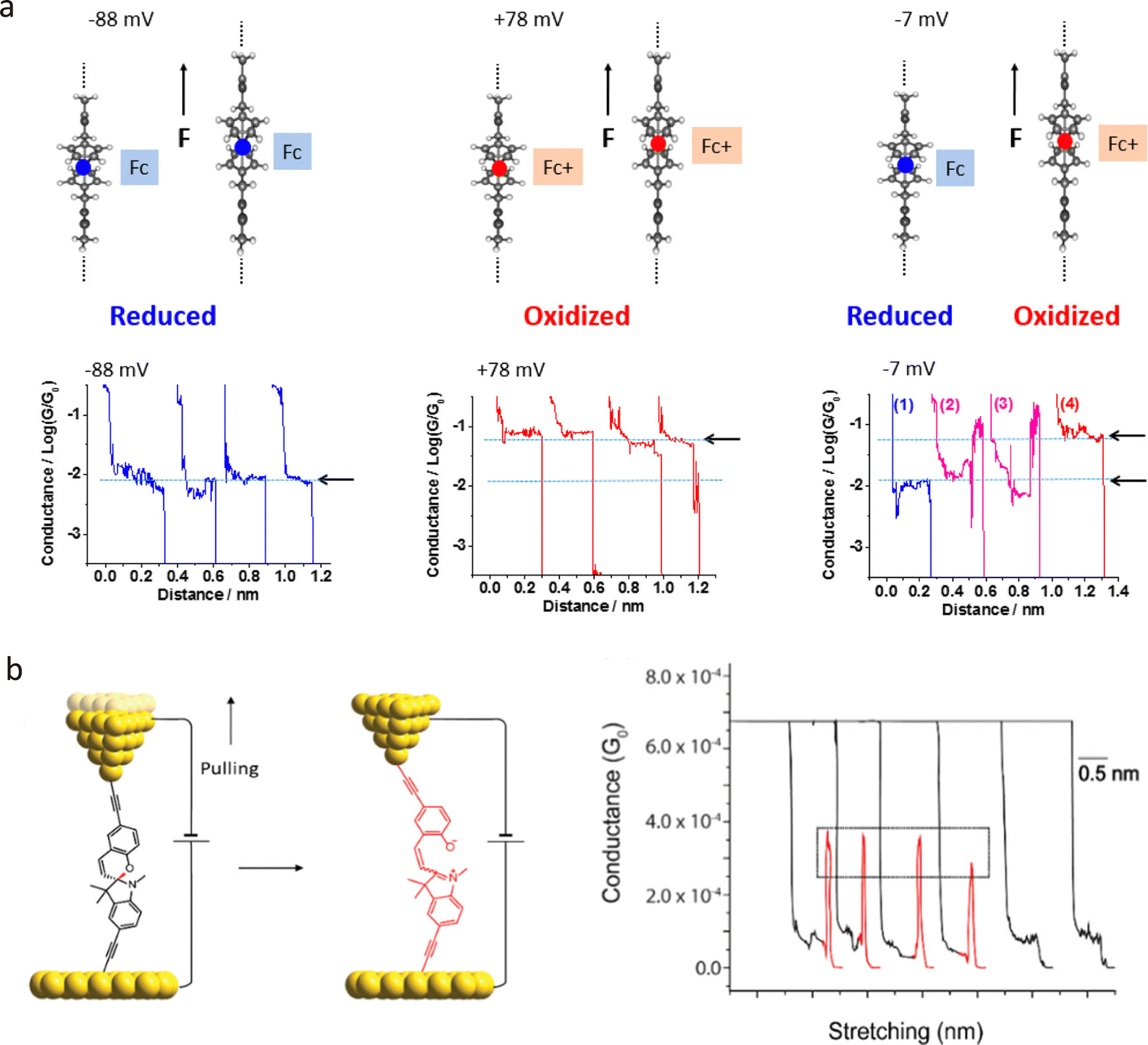 | ||
| Fig. 19 (a) Schematic and typical conductance-distance diagram of Fc and Fc+. The stretching force can induce the redox state switching at the equilibrium potential, and lead to two significant conductance states. (b) Schematic illustration of the isomerisation of spiropyran to merocyanine induced by the stretching force. The C–O bond-breaking process of spiropyran results in a significant increase in conductance during stretching. Panel (a) is reprinted with permission from ref. 217, Copyright (2017), American Chemical Society. Panel (b) is reprinted with permission from ref. 219, Copyright (2019), American Chemical Society. | ||
Similarly, Riccardo et al. discovered that mechanical force could control the arrangement of the junctions in homoleptic FeII complexes. The stretching force distorted the FeII coordination sphere and eventually altered the spin state from a low-spin to a high-spin, leading to a conformational change.174 In addition, the conformation change of molecules without bond rupture can be triggered by mechanical force. For instance, Timothy et al. observed three distinct conductance states during stretching in permethyloligosilane, attributed to conformational switching of the molecule.218
Mechanical stress can also directly induce bond formation and cleavage, leading to isomerisation events. Nadim et al. reported force-induced isomerisation between spiropyran and merocyanine, as shown in Fig. 19(b). During the STM probe stretching process, the force induced the C–O bond-breaking and formation process, leading to the ring-opening and ring-closing in the parent spiropyran molecule. Consequently, two isomerisations lead to a significant change in conductance, which can be monitored at the single-molecule level. This conformational change in spiropyran exhibited single-molecule diode behaviour, with an average current rectification ratio of 5 at ±1 V. The rectification was stronger when the positively charged part was connected to the negative terminal.219,220
5.1.2.1. Single-electron-induced reaction. In quantum tunnelling platforms, an applied voltage bias between two electrodes creates an energy difference in their Fermi levels, promoting directional electron tunnelling through a molecule bridging the junction. By optimising the electrode bias and modifying the identity of the bridging molecule, electrons with a certain energy can interfere with the chemical transformations. Based on the energy of the tunnelling electrons, these reactions can be categorised into two main kinds.
Early research by Stipe et al. classified electron-induced reactions into two categories based on the energy of the tunnelling electrons.221 In the low-energy regime, electron transport occurs via inelastic tunnelling. Here, low-energy electrons are injected into the molecule and excite its vibrational modes, leading to energy exchange between the tunnelling electrons and molecular bonds. When the accumulated vibrational energy exceeds the bond dissociation threshold, electrons can induce bond cleavage, such as O–O, C–H, and C–I bonds.221–223 Additionally, low-energy electrons can induce intramolecular processes, such as hydrogen tautomerisation.224,225
In contrast, at higher bias potentials, electron transport enters the field-emission regime. High-energy electrons can access unoccupied molecular orbitals, promoting the molecule to a higher electronic state.226 These high-energy electrons can interfere with aromaticity, alter reactivity, and drive chemical transformations relevant to electrocatalysis and photocatalysis.227 This high-energy regime provides a conceptual and experimental bridge between single-molecule reactions and catalytic processes, enabling the exploration of catalytic mechanisms at molecular-level resolution.216
5.1.2.2. Single-molecule redox reaction. The configuration of quantum-tunnelling platforms requires conductive materials as electrodes. The integration of counter and reference electrodes enables electrochemical reaction activation, providing a method for investigating reaction pathways at the single-molecule scale. As shown in Fig. 20(a), adjusting the surface potential via electrochemical gating enables precise alignment of the electrode Fermi level with molecular frontier orbitals, facilitating redox transitions and quantifying electron-transfer kinetics.228,229
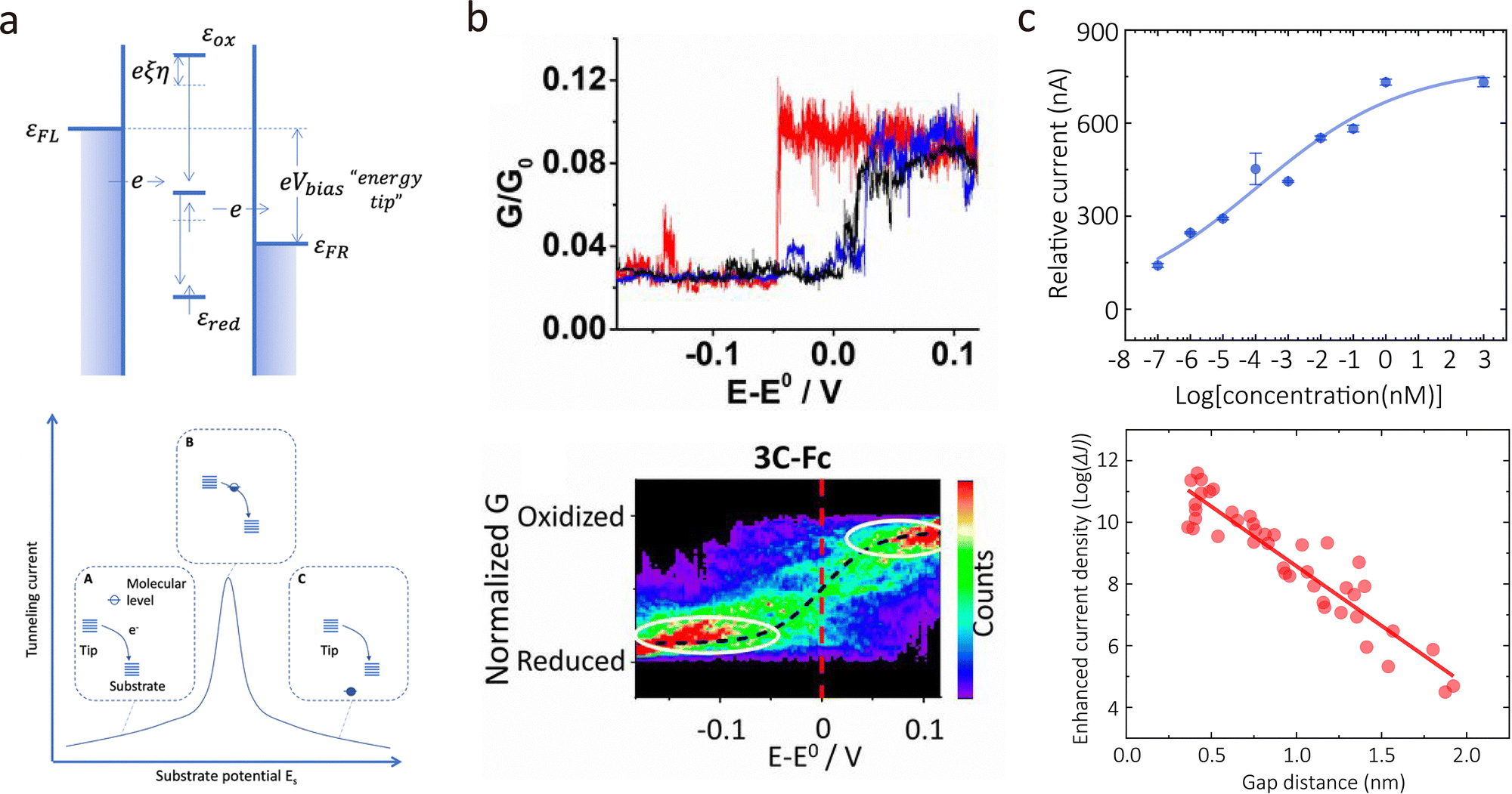 | ||
| Fig. 20 (a) Schematic energy diagram of redox active molecule set between tunnelling electrodes with a potential difference of Vbias (top). The tunnelling current/overpotential relationship. The significant current enhancement can be observed when the molecular energy level is set between the tip and substrate (below). (b) Experimental (top) and simulated (below) conductance vs. overpotential plot of 3C-Fc single molecule junction. Two distinct conductance distributions can be observed through the scanning, indicating the switching between the redox state of the ferrocene. (c) Concentration (top) and gap distance (below) relationship with tunnelling current of ferrocyanide/ferricyanide redox active couple measured through quantum mechanical tunnelling probes. Panel (a) is reprinted with permission from ref. 228, Copyright (2023), Royal Society of Chemistry. Panel (b) is reprinted with permission from ref. 235, Copyright (2019), National Academy of Sciences. Panel (c) is reprinted with permission from ref. 237, Copyright (2025), Wiley-VCH Verlag GmbH & Co. KGaA, Weinheim. | ||
Two principal approaches are typically employed to probe redox processes on the quantum tunnelling platform. In the first approach, a constant voltage bias is applied between two electrodes, while the gate potential is adjusted to align the redox-active orbital with the Fermi level of one or both electrodes. For instance, Albrecht et al. applied this approach to redox-active Os(II)/(III) complexes on STM-BJ.230 When the gate potential overlaps the redox potential of Os(II)/(III), the redox level of the molecule is brought into the energy window between the Fermi levels of the electrodes. Therefore, the electrons were able to hop through the redox-active centre from one electrode to the other, resulting in a significant enhancement of the tunnelling current. The magnitude and position of this conductance peak are sensitive to overpotential, reorganisation energy, and molecular conformation of the target molecule.229 The application of different redox-active supramolecules, transition metal complexes, and clusters on a quantum tunnelling platform demonstrates significant assistance for scientists to gain a deeper understanding not only of the hopping effect but also of the mechanism of redox-active systems at the single molecular scale.231–233
The second approach involves adjusting the electrode Fermi levels to match the redox equilibrium potential of the target molecule using cyclic voltammetry. In 2006, Tao et al. reported cyclic voltammetry (CV) measurements of a ferrocene complex using the STM-BJ technique.234 The ferrocene with an alkyl linker is functionalised between the STM-BJ to form a molecular junction. During the voltage scanning between the redox potential of the target molecule, the molecule alternated between its reduction and oxidation states, producing distinct conductance levels. The conductance state was dominated by the reduction or oxidation state, producing fluctuations in the current response. This finding explores an approach to monitoring average current rather than peaks to understand redox-cycling behaviours in a single target molecule.235 Further research by Li et al. discovered that this process is kinetic-driven, and can be illustrated through the Butler–Volmer equation.234,236 As shown in Fig. 20(b), the conductance trend of the target single molecule demonstrates a sigmoidal trend, which can be illustrated through the equilibrium electron transfer process and the Nernst equation.216,235 Extending this approach beyond SMJs, Tang et al. also observed a similar sigmoidal trend on free diffused ferrocyanide/ferricyanide couples through quantum tunnelling probes shown in Fig. 20(c). They explored the concentration of the redox-active species, and the gap distance also affected the redox cycling behaviour.237 This finding extended the application of redox cycling from single-molecule junctions to solution-phase systems.
In addition to electron hopping between molecular orbitals, quantum interference also plays a role in the electron-transfer process. When the conformation of the target molecule changes during the reaction, quantum interference produces a significant variation in conductance.238,239 Nadim et al. discovered that optimising the gate potential induced an anthraquinone-based norbornylogous molecule (SAQS) to switch between the oxidised (AQ) and reduced (H2AQ) states.240 This switch further led to a significant variation in conductance by an order of magnitude due to the linear conjugation of H2AQ and destructive quantum interference of AQ. This single-molecule electrochemical platform offers a powerful way to study structural changes during electrochemical reactions and electron catalysis.
5.1.2.3. Single-molecule electron catalysis. Electrons can also act as catalysts to activate the reactions. Unlike simple electron transfer or bond-breaking processes via high-energy tunnelling, electrons are injected into the target molecule and form a reactive intermediate that further undergoes a chemical transformation, including bond cleavage, isomerisation, coupling, etc. After the reaction, the electrons are regenerated and return to the electrode, allowing a nanoscale electrocatalytic cycle to be observed through the tunnelling junction.227 A representative example of this phenomenon was the electron-catalysed dehydrogenation of 1,2-di(4-pyridinium)ethane (DPA2+) to 1,2-di(4-pyridinium)ethene (DPE2+), reported by Chen et al. using a scanning tunnelling microscopy break junction (STM-BJ) configuration, as illustrated in Fig. 21.241 In this system, two electrons injected from the top electrode reduce DPA2+ to a diradical intermediate (DPA˙˙), which subsequently undergoes intramolecular dehydrogenation to form DPE˙˙. The product is then reoxidised as two electrons are extracted to the bottom electrode, completing the redox loop and regenerating DPE2+. Notably, this ethane-to-ethane transformation is controlled by electron flow within the junction, demonstrating the catalytic role of electrons at the single-molecule scale. The quantum tunnelling platform demonstrates significant potential for resolving the sequential steps of catalytic cycles at atomic resolution, thereby enabling understanding of the classical catalysis process and the design of new reaction pathways.
 | ||
| Fig. 21 Schematic illustration of the mechanism of electron-catalyzed single-molecule dehydrogenation of DPA2+ to DPE2+ on STM-BJ. The corresponding 1-D and 2-D conductance diagram of DPA2+ and the DPE2+ reveals the energy difference due to the dehydration on the backbone of DPA2+. This panel is reprinted with permission from ref. 241, Copyright (2021), American Chemical Society. | ||
5.1.3.1. OEEF catalysis. OEEF catalysis involves applying a directional electric field across a molecule to stabilise polarised transition states, thereby lowering activation energy barriers and enhancing reaction rates.242 As shown in Fig. 22(a), Guo et al. applied the OEEF on the 4,4′-terphenyl-4,4′-dicarboxylic acid (TTDA) single-molecule junction.243 By optimising the OEEF direction, the azobenzene side group conformation could be modulated, which efficiently altered the energy difference between the trans and cis forms of the target molecule. When the orientation of the OEEF is set to be in the same direction as the dipole moment of the activated bond in the target molecule. In Fig. 22(b), the electric field can alter the catalytic selectivity of the molecule, thereby activating the reaction. The negative bias reduced the isomerisation energy from trans to cis geometry, while the positive bias stabilised the trans geometry. By optimising the direction of the electric field, the molecular conformation produces a reversible two-mode switching effect, demonstrating significant potential for future design of single-molecule devices and logic gates.
 | ||
| Fig. 22 (a) Schematic illustration of the reversible cis/trans isomerisation of the azobenzene unit on TTDA triggered by the oriented external electric field. The conductance variation can be observed through the graphene single-molecule junction. (b) Schematic illustration of the mechanism of the voltage-dependent conductance switching. The decrease in isomerisation energy from trans to cis geometry leads to the stabilisation of the cis isomer in negative OEEF, while the trans isomers are more stable in the positive OEEF. (c) Schematic illustration of OEEF-induced Diels–Adel reaction between diene and dienophile. The negative OEEF can stabilise the transition state of the reaction intermediate, which increases the blinking frequency during the reaction. Panel (a) and (b) are reprinted with permission from ref. 243, Copyright by Linan Meng (2019), under CC BY 4.0 license. Panel (c) is reprinted with permission from ref. 244, Copyright (2016), Springer Nature. | ||
In 2016, Michelle et al. reported OEEF-induced D–A reactions between dienes and dienophiles. As demonstrated in Fig. 22(c), the strength and orientation of the OEEF can modulate reactivity by altering molecular orbital alignment and fine-tuning the energy landscape.244 Importantly, applying a negative voltage bias to the molecules resulted in a fivefold increase in the frequency of Diels–Alder adduct formation. This phenomenon is caused by the stabilisation of the transition state, which reduces the energy barrier when the OEEF aligns with the reaction dipole moment.
5.1.3.2. IEF catalysis. In bulk electrochemical systems, applying a surface potential to the electrodes induces ionic reorganisation, leading to the formation of an electrochemical double layer (EDL). This EDL plays a critical role in modulating reactivity. Similarly, the electric field can produce effects on the nanoelectrodes and interfere with reactions at the single-molecule scale.23,216 In 2022, Wang et al. experimentally demonstrated the variation in the electric double-layer geometry using STM-BJ.245 EDL geometries could be adjusted via ionic strength, bias, and gating, altering charge transport and producing variation in charge transport properties. Critically, asymmetric electrode geometries, such as a nanoscale tip versus a planar substrate, can generate IEFs by forming asymmetric electric double layers.246 This effect not only affects electron transport but also directly influences reaction kinetics by stabilising ionic transition states or reactive intermediates.198,247 For a comprehensive discussion of ionic effects in molecular electronics, readers are referred to other specialised reviews.23,245
Venkataraman et al. applied IEFs to modulate molecular reactivity and induce specific reactions on STM-BJ platforms.248 As shown in Fig. 23(a), to isolate IEF-driven effects in polar solvents and suppress the background ionic current, the conductive tip must be coated with an insulating layer. When the IEF was applied to the STM, an asymmetric polarity was produced between the tip and the substrate, which can also be considered an electroinductive effect. By modulating the potential on the electrodes, the electrode can be induced into electron-donating or electron-withdrawing states, which interfere with the bond formation. For instance, the negative tip bias selectively promotes the formation of the Au–C bonds, while the positive bias preserves the formation of the Au–I bond. Moreover, the IEF further influenced the conformational change and reactivity of the target molecule.248–250 As shown in Fig. 23(b), Venkataraman et al. applied a wax-coated Au STM tip to drive noncatalytic electrooxidative coupling of anilines. They demonstrated that a positive IEF stabilises aniline radical cations, selectively forming cis- or trans-azobenzene depending on the binding group.251 Moreover, the anchoring strategy between the molecules and electrodes can also be resolved and switched by modulating the IEF during the reaction on the STM-BJ platform. For instance, Chen et al. fabricated the BIPY-Me2+ junction through electrostatic interaction between Au and pyridinium-N+. As shown in Fig. 23(c), the IEF over −400 mV allowed electron injection into the BIPY-Me2+ and produced BIPY-Me˙+. Moreover, they discovered that electron injection occurred at a small anchoring group, whereas a large anchoring group suppressed it.252
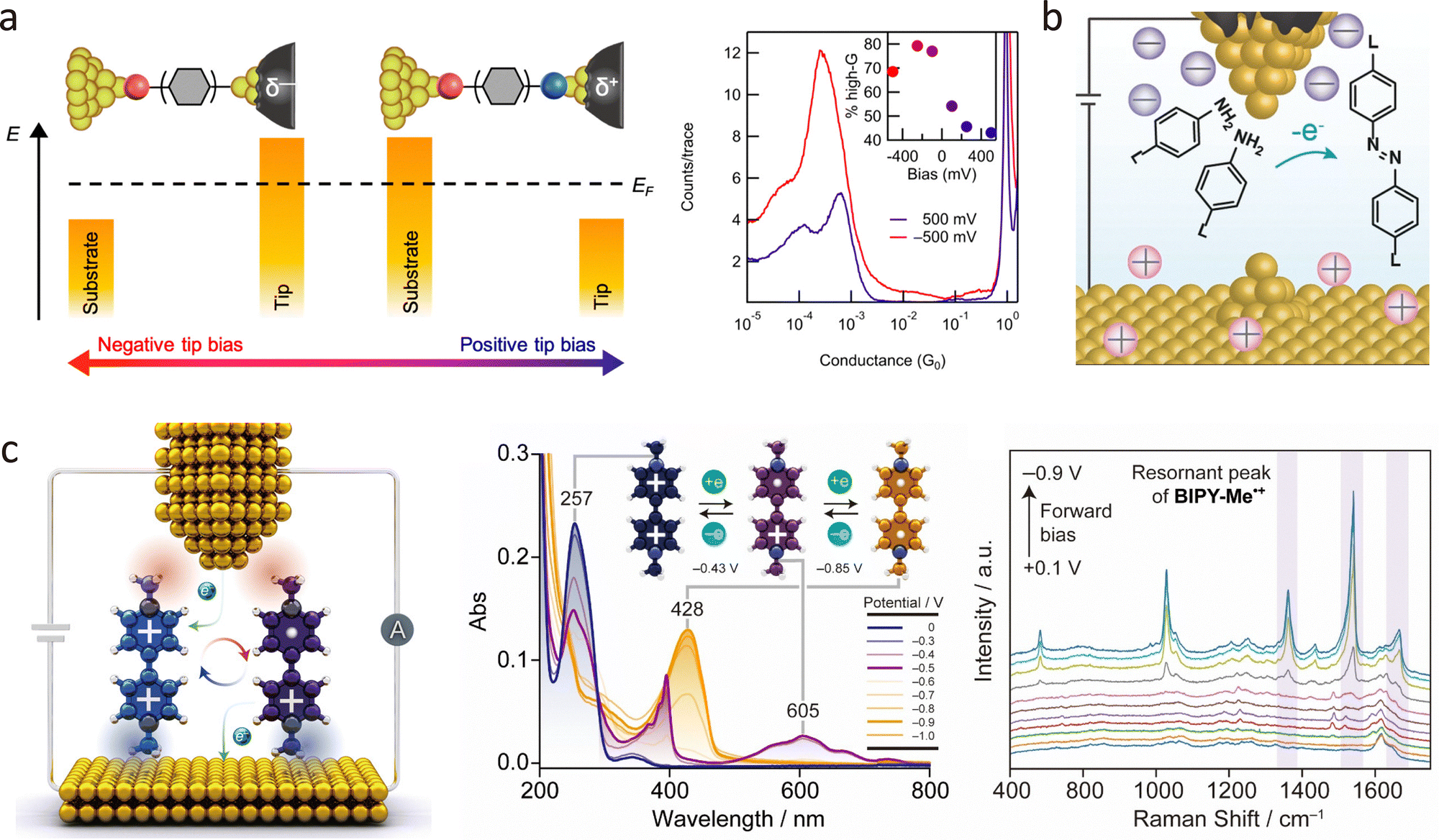 | ||
| Fig. 23 (a) Schematic illustration of the anchoring group stability under different IEF. The conductance diagram reveals that the positive tip voltage bias promotes the Au–I linkage, while the negative tip voltage bias promotes the Au–C linkage. (b) The schematic demonstration of the formation of azobenzene derivatives via electrooxidation of anilines induced by IEF in single-molecule junctions. (c) Schematic demonstration of the Electric field induced transition between BIPY-Me2+ and BIPY-Me˙+ through STM-BJ. The corresponding UV-Vis spectra and electrochemical SERs spectroscopy demonstrate the formation of BIPY-Me˙+ when applying forward voltage bias on the Au substrate. Panel (a) is reprinted with permission from ref. 248, Copyright (2020), American Chemical Society. Panel (b) is reprinted with permission from ref. 251, Copyright (2019), Wiley-VCH Verlag GmbH & Co. KGaA, Weinheim. Panel (c) is reprinted with permission from ref. 252, Copyright (2021), American Chemical Society. | ||
When light is applied to a photoactive molecule, it supplies energy that can drive conformational changes, often involving reversible bond rearrangements.254,255 Guo et al. reported the light switch of diarylethene through graphene–diarylethene–graphene molecular junctions, as shown in Fig. 24(a).256 When the light with different wavelengths was applied to the diarylethene molecule, the conformation of the diarylethene suffered a reversible isomerisation effect, and it demonstrated unique on–off characteristics in the tunnelling current response. Furthermore, further research found that the interfacial coupling between the molecule and the electrodes significantly influenced the photoswitching behaviour.180,216,257–259 These findings suggested that the switching performance of photoactive molecules could be optimised by modifying either the electrode materials or the anchoring groups.259,260
 | ||
| Fig. 24 Optically driven single-molecule reactions. (a) The schematic demonstration of the isomerisation of diarylethene under UV and visible light. This reversible open and close switch demonstrated significant conductance variation observed on I–V and I–t response. (b) Schematic illustration of the photoswitchable medium MCH-induced intermolecular proton transfer of a 1,3-azulene derivative under blue light in a single molecule junction. (c) Schematic illustration of determining the photoisomerisation process of trans and cis azobenzene through measuring the single molecule conductance. The result reveals that photoisomerisation of trans azobenzene adopts a planar structure, while cis-azobenzene adopts a non-planar conformation. Panel (a) is reprinted with permission from ref. 256, Copyright (2016), The American Association for the Advancement of Science. Panel (b) is reprinted with permission from ref. 261, Copyright (2019), Wiley-VCH Verlag GmbH & Co. KGaA, Weinheim. Panel (c) is reprinted with permission from ref. 262, Copyright (2024), American Chemical Society. | ||
In addition to directly photoresponsive molecules, light can also induce electronic excitation that drives conformational changes in non-photochromic systems. As shown in Fig. 24(b), Cai et al. reported a light-driven, reversible intermolecular proton transfer at single-molecule junctions using a diarylethene–pyridine supramolecular pair.261 By combining STM-BJ conductance measurements with UV irradiation, the distinct switching behaviour of diarylethene–pyridine is attributed to proton transfer modulated by light-induced conformational changes. Moreover, the open and closed forms of diarylethene influence hydrogen bonding and proton affinity, enabling controlled proton shuttling between donor and acceptor. Apart from observing light-driven open and closed forms of molecules, Tan et al. investigated the conductance evolution of photoisomeric single-molecule junctions under continuous UV irradiation using diarylethene derivatives in an STM-BJ setup.262 As shown in Fig. 24(c), they observed dynamic transitions from high- to low-conductance states, corresponding to isomerisation from the trans to the cis geometry. Real-time conductance monitoring reveals stochastic switching events and intermediate states, highlighting the role of UV exposure duration and intensity in modulating the distribution of isomers.
A representative example is the Diels–Alder (D–A) reaction reported by Guo et al.263 As shown in Fig. 25(a), the boc-CBP-Maleimide molecule was functionalised in the tunnelling junction to react with furan through the D–A reaction. By systematically increasing the temperature, the activation energy required for the D–A reaction was determined. Simulations of the energy landscape enabled the assignment of stable conductance states to the endo and exo conformers of the product. Furthermore, rapid current responses revealed the formation of a zwitterionic intermediate (ZI), which was observed to form preferentially at elevated temperatures.
 | ||
| Fig. 25 Thermal-driven single-molecule reactions. (a) The schematic demonstration of monitoring the D–A reaction through the graphene single-molecule junction. The current time distribution demonstrates that high temperature (left) and high composition of toluene in DMSO (right) can open more reaction trajectories crossing the reaction energy barrier, leading to the formation of more zwitterion transition states (ZI) and inducing the endo/exo product formation. (b) The schematic demonstration of the thermal-reversible D–A reactions between AnAm and C60 on STM-BJ. The corresponding conductance analysis reveals that the D–A reaction can be reversibly switched between 25 °C (red) and 60 °C (blue). Panel (a) is reprinted with permission from ref. 263, Copyright by Chen Yang (2021), under CC BY-NC 4.0 license. Panel (b) is reprinted with permission from ref. 264, Copyright (2023), Elsevier. | ||
Thermal energy can also govern the reversibility of DA reactions. As shown in Fig. 25(b), Li et al. demonstrated thermally reversible cycloaddition between anthracene-2,6-diamine and C60 at the single-molecule level using scanning tunnelling microscopy break junction (STM-BJ) techniques.264 The reaction progress was monitored via conductance changes, where the on–off transition in current corresponded to bond formation and cleavage. Notably, the reversible conductance switching between 25 °C and 60 °C highlights the potential for thermal control over bond-formation and bond-breaking events in molecular electronics.
5.2. Revealing the full reaction pathway through the quantum tunnelling platform
The molecular junction has played a significant role in understanding single-molecule behaviour by monitoring real-time tunnelling current responses. This platform can be extended to help understand the mechanism of single-molecule reactions across the fields of synthesis, catalysis, nanotechnology and materials science.216,265 The integration of multiple precise controls over reactions makes the quantum tunnelling platform a new pathway for researchers to sense single-molecule reactions. For example, as shown in Fig. 26, the graphene molecular junction can reveal the dynamics and intermediates of the Suzuki reaction. The typical current response in Fig. 26(b) indicates real-time detection of changes in the target molecules. By statistically counting the conductance state from current–time responses under different voltage bias conditions, several stable conductance states with different time intervals can be observed, as depicted in Fig. 26(c) and (d). Revealing the main intermediates produced in the Suzuki reaction. Reaction kinetics can be revealed by calculating the time interval for conductance switching, as described by the Arrhenius equation (Fig. 26(e)).266 Moreover, the integration of the OEEF and the graphene single molecule junction reveals that the inductive effect of substituents on reaction rates can be determined by inserting different functional groups at the para-position of the aromatic boronic acid. The Hammett calculation reveals that electron-withdrawing substituents on the boronic acid accelerated the Suzuki–Miyaura cross-coupling reaction. | ||
| Fig. 26 (a) Schematic illustration of revealing the reaction mechanism of the Suzuki reaction through a single-molecule junction. The catalyst functional unit is functionalised as a single-molecule junction. (b) Typical current–time response achieved from the quantum tunnelling platform. (c) Multiple conductance states and (d) corresponding conformational changes of the catalyst functional unit. (e) In addition to the conductance states information, the switching time between states can also be used to extract the reaction kinetics and conversion rates between states. This Panel is reprinted with permission from ref. 216, Copyright (2023), Springer Nature. | ||
In addition to tracking reactions on a single target molecule, the quantum tunnelling platform can be extended to investigate intermolecular reaction mechanisms. By functionalising individual reactant molecules on each side of the tunnelling electrodes, reactions between two molecules confined within the nanogap can be observed. Such configurations expand the scope of quantum tunnelling platforms to understanding intermolecular interactions during the reaction. For instance, in Fig. 27(a), Chen et al. revealed the mechanism of [2+2] and [4+4] cycloaddition between CB[8] and guest molecules PVP and AnPy with the assistance of graphene single-molecule junctions.267 Through precise control of electrode bias (Fig. 27(b)) and computational simulation of energy landscapes (Fig. 27(c)), they revealed that increasing voltage promotes electron injection into the supramolecular complex, stabilising radical intermediates and accelerating cycloaddition rates by up to 340-fold, while simultaneously inhibiting retro-reactions. Complementary DFT and Marcus theory analyses further revealed that electrical tuning reshaped the reaction coordinate, thereby lowering activation barriers (e.g., from 1.97 eV to 0.35 eV for [2+2] cyclisation) and shifting thermodynamic equilibria. This transforms the platform from a passive observer into an active manipulator of electron-catalysed pathways under nanoconfinement.
 | ||
| Fig. 27 (a) Schematic illustration of revealing the reaction mechanism of cycloaddition through the graphene single-molecule reaction. (b) The typical current–time response reveals four typical states during the [2+2] cycloaddition process. (c) The plausible mechanism for the reversible single-electron-catalysed cycloaddition and the transition rates between different reaction intermediates can be calculated from the energy profile and kinetics based on the different conductance states. This panel is reprinted with permission from the ref. 267, Copyright (2025), American Chemical Society. | ||
6. Biosensing using quantum tunnelling
Understanding the fundamental mechanisms underlying life processes remains a central goal in modern scientific research. Biomolecules such as proteins, DNA, and small metabolites serve as the essential functional units of life. Investigating their behaviour at the single-molecule level offers profound insights into the molecular principles governing biological systems. As supramolecular entities, biomolecules exhibit considerable structural complexity and undergo dynamic conformational changes—such as folding, fluctuations, and contractions—on the nanoscale. These events often occur rapidly, making them ideally suited to detection via quantum tunnelling sensors, which offer exceptional spatial and temporal resolution. As a result, quantum tunnelling platforms hold considerable promise for probing the intrinsic properties of individual biomolecules and advancing our understanding of their function in physiological contexts. In this part of the review, we focus on recent advances in the application of quantum tunnelling sensors in biological systems and explore their potential to transform single-molecule biophysics and bioanalytical science.6.1. Quantum tunnelling platform for single molecule sequencing
The discovery of the structures of DNA and proteins has fundamentally transformed the understanding of biological processes and disease mechanisms. Emerging single-molecule electrical detection-based sequencing platforms represent a transformative, accurate, cost-effective and high-throughput approach that eliminates the need for labelling or amplification. This paradigm shift began in 1989, when sequencing single-stranded DNA using membrane-embedded nanopores was proposed.268 Over the past three decades, nanopore sequencing based on biological nanopores has evolved into a commercially viable technology, enabling applications in metagenomics, personal genome profiling, and personalised medicine.269–273 However, for solid-state nanopores, achieving single-nucleotide resolution remains challenging due to the rapid, stochastic nature of DNA translocation and the limitations of ionic current-based readouts.268,274,275 Quantum tunnelling sensors, with their superior spatial and temporal resolution, offer a compelling alternative for direct structural interrogation of DNA and proteins at the single-molecule level using solid-state-based technologies. Recent innovations in transverse tunnelling current measurements have shown promise for enhancing base identification precision.270,273Unlike nanopore systems, quantum tunnelling platforms lack intrinsic mechanisms to guide molecules into the sensing region. To overcome this, various control strategies have been developed. For instance, Ivanov et al. developed a protocol for fabricating a solid-state nanopore aligned with a tunnelling junction.276,277 As shown in Fig. 28(a), λ-DNA translocation events were detected simultaneously in both the ionic and tunnelling currents. However, limitations in time resolution, translocation speed, and nonspecific adsorption hinder single-nucleotide discrimination.
 | ||
| Fig. 28 (a) Schematic diagram of tunnelling gap integrated nanopore. DNA is inserted in the bottom reservoir and electrophoretically driven through the nanopore and the tunnelling junction. The tunnelling current and ion current can be measured when DNA passes through the device. (b) Schematic diagram of a DNA heteropolymer (d(CCACC)) in the STM gap. Characteristic current spikes produced by dAMP and corresponding distribution of pulse heights. (c) Schematic diagram of DNA sequencing with MCBJ and corresponding conductance histogram of four nucleotides. (d) Single-molecule detection with quantum tunnelling probe. The scatter plot demonstrates the typical current transients for each mononucleotide. Panel (a) is reprinted with permission from ref. 276, Copyright (2010), American Chemical Society. Panel (b) is reprinted with permission from ref. 278, Copyright by Takahito Ohshiro (2012), under CC BY-NC-SA 3.0 license. Panel (c) is reprinted with permission from ref. 273, Copyright (2012), Springer Nature. Panel (d) is reprinted with permission from ref. 34, Copyright by Longhua Tang (2021), under CC BY 4.0 license. | ||
Huang et al. introduced a method using STM-BJ with 4-mercaptobenzamide-functionalised probes and substrates to form hydrogen bonds with nucleotides, thereby prolonging their residence time in the tunnelling gap.278 As shown in Fig. 28(b), this enabled the detection of characteristic current spikes and demonstrated that DNA oligomers produced signals comparable to single nucleotides, laying the groundwork for tunnelling-based sequencing. Another strategy focuses on reducing the precise nanogap distance. Using mechanically controlled break junction (MCBJ) technology, the nanogap can be controlled with an accuracy of single nanometre, matching the size of a single nucleotide.279 Ohshiro et al. used this approach to distinguish conductance signals among the four DNA bases, as illustrated in Fig. 28(c).273 Additionally, they employed a random retesting method, in which DNA/RNA fragments were randomly cleaved and sequenced multiple times. Computational algorithms then reconstructed the full sequence by aligning overlapping regions from fragmented reads. In addition to the dynamic tunnelling platforms, Tang et al. applied quantum tunnelling probes to sequence the DNA shown in Fig. 28(d).34 This provides a convenient and straightforward solution for the preparation of small gap tunnelling electrodes. Tunnelling measurements on individual deoxyribonucleoside monophosphates (dNMPs) revealed distinct conductance profiles for dAMP, dGMP, dCMP, and dTMP.
In addition to direct sequencing, quantum tunnelling sensors are highly sensitive to subtle conformational changes in macromolecules, enabling enzyme-based detection strategies. Pugliese et al. immobilised DNA polymerase I Klenow fragment (KF) onto a single-walled carbon nanotube field-effect transistor.280 As shown in Fig. 29(a), through real-time monitoring of the doping kinetics for both natural and chemically modified dNTPs, chemically modified dNTPs substantially prolonged nucleotide recognition times but did not affect the kinetics of KFs closed conformational state. Further analysis indicated that KF dynamically assesses base-pair electronic structure and stability via O-helix conformational changes, demonstrating notable tolerance to modified dNTPs. These findings provide critical insights into DNA polymerase mechanisms and advance the development of novel sequencing strategies.
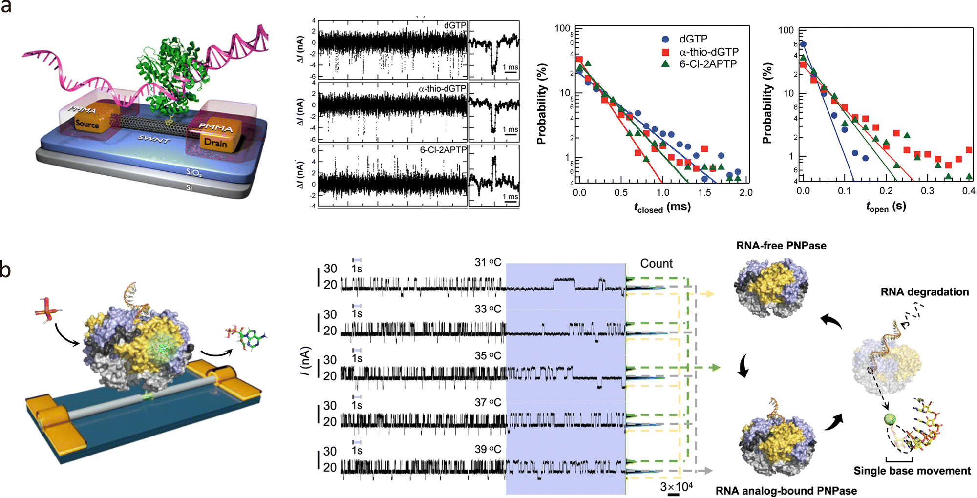 | ||
| Fig. 29 (a) Schematic illustration of detecting the doping mechanism of dNTPs analogs through a single KF nanocircuit. According to the I–t traces, the changes in the open and closed time of KF caused by the incorporation of dNTP and its analogs. (b) Schematic diagram of a SiNW FET device decorated with a single PNPase molecule. Real-time current responses demonstrate the PNPase structural transformation before the addition of RNA analog [poly(A)30] (right top panel), after the addition of RNA analog [poly(A)30] (right middle panel) and after further addition of H3PO4 (right bottom panel). Panel (a) is reprinted with permission from ref. 280, Copyright (2015), American Chemical Society. Panel (b) is reprinted with permission from ref. 281, Copyright by Zhiheng Yang (2023), under CC BY 4.0 license. | ||
Similarly, Yang et al. used a silicon nanowire field-effect transistor (SiNW FET) to analyse in real time the dynamic mechanism of RNA analogue degradation by Escherichia coli multinucleotide phosphorylase (PNPase).281Fig. 29(b) demonstrates the configuration of a single PNPase junction. A single PNPase molecule was conjugated to the molecular bridge on the surface of the SiNW through a thiol–maleimide–Michael addition. Upon introducing RNA analogues, a distinct conductance shift was observed, followed by third-order conductance fluctuations after phosphate addition. They assigned the middle and low-conductance states to the PNPase-RNA analogue complex and free PNPase, respectively, while the high-conductance state corresponded to the RNA degradation intermediate. It is worth noting that with the substrate poly(A)30, they observed exactly 30 fluctuations (the same number of nucleotides as in the RNA analogue), demonstrating single-base resolution.
6.2. Revealing biological functions at the single-molecule scale
Quantum tunnelling platforms offer unique opportunities to investigate the functional dynamics of biomolecules with sub-nanometre spatial precision and microsecond temporal resolution. By linking conformational changes and electron tunnelling pathways to measurable electrical signals, tunnelling sensors have enabled the real-time observation of protein action in biological behaviours, demonstrating the potential of quantum tunnelling platforms not only for fundamental mechanism investigations but also for the development of biosensors and bioelectronic systems.57Electron transfer is a crucial step in many fundamental cellular processes, including respiration and photosynthesis. Investigating the electron transfer mechanisms can help understand biochemical processes and life activities.57,228,282 Single-molecule electronics provide a powerful approach for studying electron transfer processes in biomolecules. The initial research focused on metalloproteins, natural redox molecules that play a crucial role in electron transfer during biochemical reactions. These proteins facilitated efficient charge transfer through electrochemical state switching at their redox centres (typically metal ions). For instance, functionalising the Pseudomonas aeruginosa blue protein (Az) on an Au substrate containing a Cu centre, the electrochemical behaviour was studied using in situ STM/STS. A current switching ratio of 9:1 was observed near the equilibrium potential, suggesting a two-step electron-transfer mechanism.228
Moreover, the quantum tunnelling platform can also uncover new fundamental mechanisms of proteins at the single-molecule scale. For instance, non-redox active proteins are typically considered insulators. However, recent studies have shown that some non-redox proteins can also effectively mediate electron transport.57,85 Lindsay et al. reported the conductance of streptavidin on an STM-BJ platform, as shown in Fig. 30(a). Through measuring the conductance of single streptavidin through biotin binding, three significant conductance distributions can be observed regardless of the variation in probe materials.283 Moreover, Tang et al. discovered that the conductance of streptavidin is closely related to the potential change.85 By fabricating a single-molecule junction on quantum tunnelling probes, this configuration (Fig. 30(b)) enabled stable current–time measurements for up to two hours. As the voltage was scanned from −300 mV to 0 mV, streptavidin exhibited transitions between conductance states. Statistical analysis revealed at least two conductance states at each bias, suggesting the presence of two or more distinct electron transfer pathways within the streptavidin-coupled tunnelling junction. While the exact mechanism of protein conductance requires further elucidation, the quantum tunnelling sensor provides a robust platform for studying dynamic conformations and mechanisms in biomolecules.
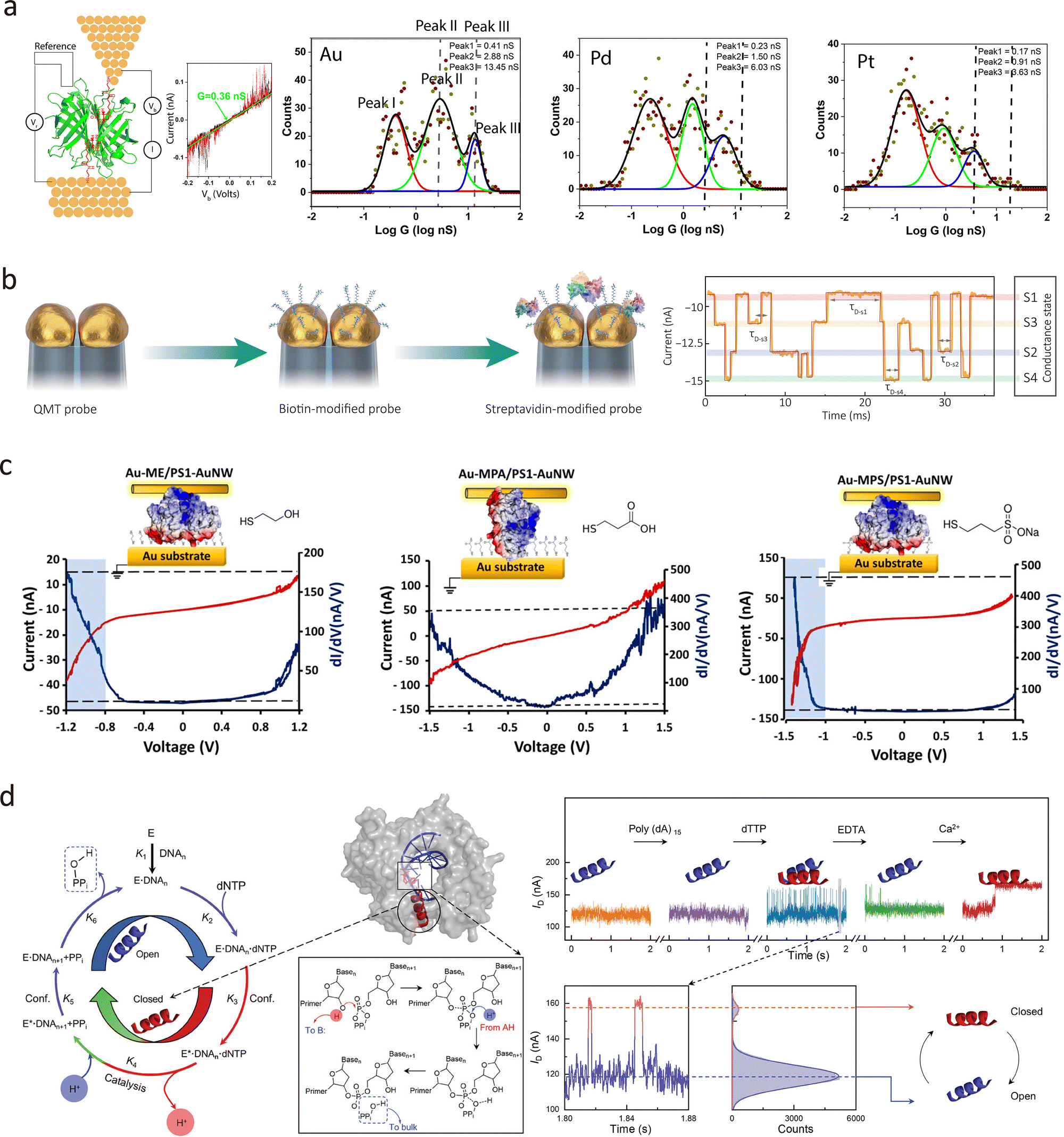 | ||
| Fig. 30 (a) Schematic illustration of streptavidin molecular junction and corresponding conductance distribution through Ag, Pd and Pt probe. Three conductance distributions can be observed on the conductance count diagram. (b) Construction of a single streptavidin molecule junction through the biotin-modified tunnelling probe. The corresponding current–time trace under – 300 mV demonstrates that there are four conductance states in streptavidin, indicating four possible electron transport pathways. (c) Schematic illustration of Anchoring PS1 in different orientations between gold electrodes through different linkers leads to different conductance properties. (d) Schematic illustration of nucleotide addition catalytic cycle of human Pol β (hPol β) through monitoring the conductance changes in the hPol β catalytic process. Panel (a) is reprinted with permission from ref. 283, Copyright (2020), American Chemical Society. Panel (b) is reprinted with permission from ref. 85, Copyright by Longhua Tang (2022), under CC BY 4.0 license. Panel (c) is reprinted with permission from ref. 284, Copyright (2023), American Chemical Society. Panel (d) is reprinted with permission from ref. 285, Copyright (2024), Advanced Science published by Wiley-VCH GmbH. | ||
Beyond monomeric proteins, quantum tunnelling platforms can also reveal the structural properties of complex biological systems. For instance, Photosystem 1 complex (PS1) is one of the most efficient natural systems for light harvesting and conversion. Through constructing an Au-linker/PS1/Au NanoWire (AuNW) configuration, Fereiro et al. discovered a directional rectification phenomenon in PS1. By applying different linkers, namely mercaptopropanoic acid (MPA), 2-mercaptoethanol (ME), and 3-mercapto-1-propanesulfonate (MPS), PS1 was anchored on the substrate in different orientations between the Au substrate and AuNW. The current–voltage characteristics of PS1 revealed a tenfold difference in absolute conductivity value at a voltage bias of −1.5 V in the Au-ME/PS1 Au and Au-MPS/PS1 Au systems.284 (Fig. 30(c)) Further ultraviolet photoelectron spectroscopy (UPS) revealed that through altering the overall orientation of PS1, the intrinsic dipole direction of PS1 can be modulated, thereby changing the rectification direction. These findings provide important insights into electron transport in photosynthetic proteins and demonstrate how tunnelling junctions can probe orientation-dependent charge transport.
Moreover, the high spatiotemporal resolution of quantum tunnelling platforms enables the observation of inner conformational changes, such as vibrations, rotations, and stretches of proteins and enzymes. For instance, Zhao et al. investigated the mechanism of Pol-catalysed DNA synthesis based on graphene field-effect transistors. As shown in Fig. 30(d), through fabricating the Pol single molecule junction on graphene nanogap electrodes, the structural changes during the Pol catalytic process were monitored in real time through current–time signals.285 They found that Pol undergoes a transition between high- and low-conductivity states during catalysis, corresponding to the enzyme's closed and open states. Isotope experiments further revealed that a proton relay (involving 3′-OH deprotonation and PPi protonation) occurs in the closed state and represents the rate-limiting step for PPi formation.
STM has been widely employed to construct single-protein molecular junctions for studying protein electron transport mechanisms at the single-molecule level. In Fig. 31(a), Zhang et al. systematically investigated the roles of both specific and non-specific contacts.286 Bivalent antibodies (IgG and IgE), providing two antigen-binding sites, and streptavidin, providing four biotin-binding sites, were employed to construct specific contacts. They found that the current was detectable only when the protein was specifically bound to at least one of the two electrodes. Furthermore, when an antibody specifically bound to both electrodes via antigen epitopes, the resulting molecular junction produced two peaks in the conductance distribution histogram. However, when the antibody was specifically bound to one end of the electrode via the antigen epitope, and the other end is connected via mercaptoethanol, the resulting conductivity distribution showed only one peak, similar to the low-conductivity peak in the previous configuration. This result indicates that specific ligand binding provides an efficient electron-injection pathway.
 | ||
| Fig. 31 (a) Schematic diagram of protein connection between gold electrodes and possible different bonding modes between the protein and the gold electrode. The connection of protein can be monitored through I–V response. (b) Schematic illustration of the NAD+ binding on the FAD. The corresponding 1D conductance histograms demonstrate clear distribution of of pure solvent (blue), FDH (pink), FDH-NAD+ (purple) and FDH-NADP+. (c) Schematic illustration of monitoring the catalytic cycling process of FDH through STM. The one-dimensional conductance histograms and statistical analysis reveal the possible intermediate states and their transformations in FDH catalysis. Panel (a) is reprinted with permission from ref. 286, Copyright by Bintian Zhang (2019), under CC BY-NC-ND 4.0 license. Panel (b) is reprinted with permission from ref. 287, Copyright 2020, Elsevier. Panel (c) is reprinted with permission from ref. 288, Copyright (2023), Springer Nature. | ||
In addition to probing electron transport, quantum tunnelling platforms can monitor biochemical reactions at the single-protein level. For instance, formate dehydrogenase (FDH) is a key oxidoreductase that catalyses the oxidation of formic acid to CO2, and its reaction typically requires cofactors. Zhuang et al. studied the electron transport characteristics of a single FDH system with STM-BJ.287 As shown in Fig. 31(b), the active FDH was immobilised between two gold electrodes using Au–S bonds from L-cysteine, and then the typical coenzyme nicotinamide adenine dinucleotide (NAD) was added to the solution to investigate the correlation between biological activity and its electron transport ability. The absorbance measurements revealed that enzyme activity increased with increasing NAD concentration. In addition, through flicker noise analysis, they found that the noise power of FDH scales as G1.9, suggesting that through-space transport dominated charge transfer. However, the noise power of FDH-NAD was scaled as G + 1.6 with a bias towards through-bond transmission. DFT calculations further indicate that the NAD embedding reduces energy-level gaps, forms efficient electron-transport pathways, and is highly positively correlated with enzyme activity.
In a subsequent study, Zhang et al. further studied the different reaction states in the formate dehydrogenase catalytic cycle. (Fig. 31(c)) Real-time conductance measurements allowed identification of five distinct intermediate states: T1, T2, T3, T4, and T5, each characterised by unique conductance peaks.288 Clustering analysis was employed to map the transitions between these intermediates and to investigate the possible catalytic pathways. It is worth noting that although a large number of conductance trajectories were statistically analysed, it was challenging to capture the deacetylase state (T5) involved in the FDH catalytic pathway, indicating that the deacetylase state (T5) proposed in the traditional Theorell–Chance mechanism may be bypassed in the FDH catalytic cycle. Through their work, the quantum tunnelling platforms place significant emphasis on real-time monitoring of protein structural variation, which helps explore biological behaviours at the single-molecule scale.
6.3. Single-molecule bioelectronic sensors
Single-molecule electronics enable real-time, high-sensitivity detection of interactions within or between individual molecules, offering a promising pathway for constructing ultra-sensitive biosensors. A critical challenge in this approach is establishing reliable connections between biomolecules and electrodes. Molecular bridges are required to form charge-transport pathways with well-defined structures, each containing suitable terminal groups that bind to the electrodes. Based on the function of biomolecules, molecular-bridge-based biosensors can be categorised into two main types: biomolecules as probe molecules on molecular bridges, and biomolecules that act as molecular bridges.289The molecular bridges require high conductivity and a typical bridge-like geometry. Thus, among biological molecules, DNA, RNA, and protein α-helices are first considered as suitable bridges to link two electrodes. Both sides of the bridge are functionalised with terminal groups that can assemble with electrodes via dielectrophoresis.290,291 To ensure that only one probe molecule is detected at a time, one specific conjugation site is fabricated in the middle of the bridge. Subsequently, a probe molecule that interacts with the target molecules is selected for conjugation to the molecular bridge, enabling specific detection of the target molecules. There are various forms of biological probe molecules, including DNA oligos, aptamers, antibodies, antigens, and certain enzymes. The ssDNA molecule can interact with another ssDNA molecule, forming a bound-state DNA duplex that enhances the conductance state. The ssDNA tether can also bind IgG antibodies via the introduction of a fluorescein antigen, forming a sandwich-like structure. An aptamer is another type of oligonucleotide characterised by high specificity and selectivity. It can bind with polymerase enzymes and produce significant, broad current transients. Hence, single-molecule electronic biosensors using such conductive molecular bridges show great promise for practical applications in biomedical diagnostics.292
Beyond serving as conductive linkers, DNA and RNA possess sequence-specific self-assembly capabilities and dense chemical functionality, enabling them to act as nanoscale devices. For instance, Tao et al. reported bridging ssRNA between the tunnelling junctions. The bridging RNA, a single-molecule junction between nanoelectrodes, serves as a sensing platform to detect pathogenic bacterial strains via transcribed RNA sequences. The RNA fragments can hybridise with the bridged RNA and produce tunnelling current variation, which can identify RNA mismatch with a detection limit on the aM scale.293 Moreover, the self-assembly properties of DNA can also be utilised as a natural biological switch. Tomoaki et al. introduced a DNA zipper configuration on STM-BJs.294 This kind of DNA zipper structure demonstrated not only enhanced conductance through π-stacked base-pair delocalisation but also enabled spontaneous reformation of the junction after disruption. These works demonstrated the potential of DNA-based junctions as label-free, biocompatible components in future bioelectronic systems.
In addition to the RNA/DNA hybrid, the DNA molecule is sensitive to its environment and undergoes conformational changes, which can be monitored through conductance switching. For example, Guo et al. reported that Ethidium bromide (EB) can intercalate the duplex and reduce DNA charge transport. The environmental effect on the interaction between DNA can also be detected. The presence of K+ or Mg2+ induced the 15-mer thrombin aptamer to form a G4 conformation, resulting in a high binding affinity with thrombin.
The in-depth investigation of biomolecular electrical properties at the single-molecule level has led to further research on the construction of novel molecular electronic devices, in which individual biomolecules serve as functional components integrated into electronic circuits. For instance, Qiu et al. reported printable logic circuits based on protein complexes.295 (Fig. 32(a)) The high-density unidirectional self-assembly of PS1 on the electrode surface was achieved through hydrogen bonding between fullerene derivatives (carboxylic acid groups of PCBA) and PS1, forming an anisotropic monolayer. The collective arrangement of dipole moments produced a significant rectifying effect (diode function). Meanwhile, the methyl ester group of PCBM led to a random orientation of PS1, forming an isotropic monolayer that exhibits symmetric conductivity (as indicated by the resistance function). Then, by printing EGaIn electrodes, PS1 diodes (PCBA substrate), and resistors (PCBM substrate), the components were successfully integrated, enabling the construction of AND and OR logic gates. This work presents a facile and reproducible route to fabricate protein-based molecular circuits, demonstrating the feasibility of utilising biomolecules in integrated molecular electronics.
 | ||
| Fig. 32 (a) Schematic illustration of the Aumica/PCBA//PS1//EGaIn junctions (left) and corresponding LogJ and LogR versus voltage responses, demonstrating significant diode features. (b) Schematic illustration of incoherent tunnelling through single strand DNA (ssDNA) and coherent tunnelling through double strand DNA (dsDNA) in Au-linker-DNA15-Fc//GaOx/EGaIn junction. (c) Schematic illustration of Cu//graphene//AfFtnAA//GaOx/EGaIn biomolecular tunnel junction. The electron tunnelling from graphene to ferritin through incoherent tunnelling, while coherent tunnelling occurs from ferritin to EGaIn. Panel (a) is reprinted with permission from ref. 295, Copyright (2022), Springer Nature. Panel (b) is reprinted with the permission from ref. 296, Copyright (2021) by Nipun Kumar Gupta, under CC-BY-NC-ND 4.0 License. Panel (c) is reprinted with the permission from ref. 297, Copyright (2022) by Nipun Kumar Gupta, under CC-BY 4.0 License. | ||
Moreover, Nijhuis et al. investigated the potential of functionalised DNA as bioelectronics. As shown in Fig. 32(b), DNA-based junctions were fabricated by single-stranded (ssDNA) and double-stranded DNA (dsDNA) monolayers assembled between electrodes.296 They found that dsDNA, with its ordered π-stacked base pairs, produced conductance up to ∼30 times greater than disordered ssDNA. Further study of the conductance revealed that dsDNA enabled coherent tunnelling across stacked bases, whereas ssDNA primarily relied on inefficient, thermally activated hopping pathways. This work provided direct evidence that conformational order within biomolecules governs the transition between coherent and incoherent charge transport, highlighting structural organisation as a critical design factor in DNA electronics.
Expanding on this, Nijhuis et al. also discovered graphene–ferritin biomolecular junctions and revealed the role of electrode interfaces in electron transport.297 As shown in Fig. 32(c), by assembling ferritin proteins onto graphene electrodes to form a Cu//graphene//AfFtnAA//GaOx/EGaIn tunnelling junction, they demonstrated temperature-dependent coherent tunnelling behaviour, which could be tuned by varying iron loading within the protein core. The measurements showed that both the charge-transport efficiency and its temperature response were strongly modulated by the Dirac-cone shape of graphene's density of states, underscoring the pivotal role of electrode–biomolecule coupling. This study not only established ferritin as a robust bioelectronic element but also revealed the potential of graphene as a platform for probing and controlling biomolecular charge transport.
Based on prior findings that streptavidin conductance can be modulated by voltage bias, Lindsay et al. revealed that the conductance states of streptavidin were also influenced by the spatial arrangement of biotin-binding sites within its tetrameric structure.298 As shown in Fig. 33(a), this finding suggested that electron transport pathways in the protein can be tuned by optimising the geometry of biotin–streptavidin interactions. By functionalising STM probes and substrates with engineered streptavidin tetramers, they successfully constructed molecular junctions incorporating doubly biotinylated Φ29 polymerase. The conductance of these junctions was shown to depend critically on the binding configuration of streptavidin, highlighting the protein's role as a controllable bioelectronic connector, as demonstrated in Fig. 33(b).
 | ||
| Fig. 33 (a) Schematic illustration of the four binding sites for streptavidin tetramers to bind with biotin. The streptavidin can be functionalised in between the electrochemical STM through different binding. (b) By optimising the anchoring position on the streptavidin, the conductance of the streptavidin-Φ29 polymerase-streptavidin single molecule junction demonstrated significant conductance variation. This panel is reprinted with permission from ref. 298, Copyright (2021), American Chemical Society. | ||
6.4. AI-assistance to understand the complex biological behaviours in the quantum tunnelling platform
Although single-molecule quantum tunnelling sensors offer powerful capabilities for probing biological processes at the molecular level, their exceptional sensitivity also presents substantial challenges in data interpretation. Several factors contribute to this complexity. First, environmental fluctuations introduce noise that can obscure weak tunnelling signals. Second, the stochastic nature of single-molecule events necessitates the collection of large datasets, making statistical analysis demanding. Third, the intricate geometry and dynamic behaviour of biomolecules make it challenging to correlate structural features with electrical signals directly. Finally, the high dimensionality and volume of the data make manual interpretation impractical. To overcome these obstacles and uncover meaningful relationships between tunnelling signals and biomolecular dynamics, artificial intelligence (AI) techniques have emerged as powerful tools for managing and analysing complex single-molecule datasets.289,299–301For example, the structural and chemical similarities among biomolecules, such as amino acids and nucleotides, often lead to highly similar, difficult-to-distinguish tunnelling signals. To identify different amino acids, Zhao et al. applied the support vector machine (SVM) to identify structurally similar amino acids: glycine (Gly) and N-methylglycine (mGly), the L- and D-enantiomers of asparagine (Asn), and the isobaric amino acids leucine (Leu) and isoleucine (Ile).302 As shown in Fig. 34(a), the STM tip and substrate were functionalised by 1H-imidazole-2-carboxamide (ICA) to achieve recognition tunnelling with amino acids. By extracting multidimensional features in both the time and frequency domains from the current–time response, SVM revealed that while individual features showed significant overlap for each pair, combining two or more features increased.
 | ||
| Fig. 34 (a) Schematic illustration of single molecule measurement of four types of adenosine phosphate molecules and the corresponding confusion matrix for recognition of four types of adenosine monophosphate molecules. (b) Schematic illustration of the detection of amino acid molecules through recognition tunnelling. The chiral enantiomers D-Asn and L-Asn, Gly and mGly and the isobaric isomers Leu and Ile are identified through probability densities. (c) Distinguish multiple conductivity states of a single protein through clustering. The optimal number of clusters is based on the internal evaluation indicators of clustering. Panel (a) is reprinted with permission from ref. 302, Copyright (2014), Springer Nature. Panel (b) is reprinted with the permission from ref. 303, Copyright (2021) by Yuki Komoto, Licensee MDPI, Basel, Switzerland, CC-BY 4.0 License. Panel (c) is reprinted with the permission from ref. 304, Copyright (2023) SIOC, CAS, Shanghai, & Wiley-VCH GmbH. | ||
Similarly, Komoto et al. demonstrated the differentiation of adenosine monophosphate analogues using a MCBJ system.303 As shown in Fig. 34(b), for each detected signal, thirteen feature parameters were extracted: peak current (Ip), average current (Iave), duration time (td), and ten shape factors (Sn = In/Ip, where n = 1, 2, …, 10). A random forest classifier was then employed to classify the signals from the four molecules based on these features. These studies demonstrate the high resolution achievable with tunnelling current for identifying highly similar molecules, and the contribution of multidimensional feature extraction combined with machine learning analysis to enhancing molecular recognition accuracy.
To minimise the interference of subjective human judgement in signal processing, Yang et al. proposed an unsupervised clustering approach to determine the conductance-state variation switch of streptavidin measured via single-molecule junctions.304 As shown in Fig. 34(c), quantum tunnelling probes were used to measure the electrical conductance of individual protein molecular junctions. By classifying initial conductance clusters under different voltage bias gradients, several metrics, including the Calinski–Harabasz (CH) index, Davies–Bouldin (DB) index, and Silhouette Coefficient, were computed to evaluate inter-cluster separation and intra-cluster cohesion, enabling the identification of the optimal cluster number that maximises both criteria. Critically, the optimal cluster number corresponded to the most probable number of distinct conductance states for the protein, yielding the most likely protein configuration under the given bias voltage. Furthermore, features of each conductance state, such as amplitude and dwell time, could be extracted. Consequently, these approaches demonstrate that AI-driven classification and clustering can substantially enhance the interpretability and precision of quantum tunnelling data, offering new strategies to decode complex single-molecule behaviours in biological systems.
7. Conclusions and perspectives
Quantum tunnelling junctions have emerged as a powerful and versatile platform for probing charge transport, molecular conformational dynamics, and nanoscale sensing with atomic-level precision. This review examined state-of-the-art fabrication strategies for static, dynamic, and passive tunnelling junctions, evaluating their respective strengths and limitations in achieving sub-nanometre resolution, device reproducibility, and measurement stability.Recent advances in quantum tunnelling sensors enabled real-time investigation of electron transport mechanisms and molecular behaviours, including quantum interference effects, conformational switching, and intermolecular interactions. These developments have not only deepened our understanding of fundamental molecular electronics but have also opened new avenues for transformative applications in biosensing, catalysis, and dynamic single-entity analysis.
Despite these significant achievements, several key challenges remain that must be addressed to fully realise the potential of tunnelling-based sensors for broader scientific and technological deployment. Three interrelated research frontiers will be critical in shaping future progress:
7.1. Scalable manufacturing and devices integration
To transition quantum tunnelling sensors from laboratory-scale demonstrations to real-world applications, scalable, cost-effective, and reproducible fabrication methods must be developed. This includes high-throughput strategies for producing sub-5 nm nanogaps with precise geometries and minimal device-to-device variation. Furthermore, the seamless integration of tunnelling platforms with microfluidic systems, soft and stretchable electronics, and biocompatible interfaces will be essential for in situ molecular detection in physiologically relevant environments. Such integration will be pivotal for next-generation biosensing, point-of-care diagnostics, and environmental monitoring.7.2. Mechanisms elucidation and resolution enhancement
While the theoretical framework of quantum tunnelling is well established, its practical manifestation at the single-molecule level often involves complex and dynamic behaviours that challenge existing models. A major obstacle is the variability observed across repeated measurements of nominally identical molecules, driven by junction rearrangements and environmental fluctuations. Addressing this variability, while simultaneously enhancing spatial and temporal resolution, will be essential for capturing transient conformational transitions, orbital hybridisation effects, and charge delocalisation pathways. The integration of tunnelling junctions with ultrafast spectroscopies, ultrasensitive current feedback systems, and precise atomic-scale junction control promises deeper mechanistic insight and access to previously unexplored regimes of molecular-scale quantum phenomena.7.3. Data correlation and AI-augmented interpretation
Reliable interpretation of single-molecule tunnelling data remains a significant challenge due to the stochastic nature of molecular interactions and signal fluctuations. The integration of artificial intelligence, machine learning, and computational simulations is poised to transform data processing, enabling rapid feature extraction, noise discrimination, and classification of complex conductance behaviours. AI-driven models can be trained to infer molecular structures, redox states, and binding modes from high-dimensional datasets. When combined with experimental data, advanced AI models, and appropriate simulations, this approach will establish robust structure–function correlations, thereby accelerating molecular design and revealing changes in molecular conformation.Together, these directions will drive the evolution of quantum tunnelling sensors to powerful, scalable tools for nanoscale characterisation and single-molecule detection. Through advances in fabrication, theoretical modelling, and data-driven analytics, tunnelling-based single-molecule sensors are poised to redefine the frontiers of physics, chemistry, biology, and nanotechnology.
Conflicts of interest
There are no conflicts to declare.Data availability
No primary research results, software or code have been included, and no new data were generated or analysed as part of this review.Acknowledgements
The authors are grateful for support from the National Natural Science Foundation of China (grant no. 62127818, 22374129), the Natural Science Foundation of Zhejiang Province (grant no. LR22F050003) and the Leading Innovative and Entrepreneur Team Introduction Program of Zhejiang (2024R0100).References
- T. Albrecht, Electrochemical tunnelling sensors and their potential applications, Nat. Commun., 2012, 829, DOI:10.1038/ncomms1791.
- Y. Zhao, W. Liu, J. Zhao, Y. Wang, J. Zheng, J. Liu, W. Hong and Z.-Q. Tian, The fabrication, characterization and functionalization in molecular electronics, Int. J. Extreme Manuf., 2022, 4, 022003, DOI:10.1088/2631-7990/ac5f78.
- E. M. Dief, P. J. Low, I. Díez-Pérez and N. Darwish, Advances in single-molecule junctions as tools for chemical and biochemical analysis, Nat. Chem., 2023, 15, 600–614, DOI:10.1038/s41557-023-01178-1.
- S. Lindsay, J. He, O. Sankey, P. Hapala, P. Jelinek, P. Zhang, S. Chang and S. Huang, Recognition tunneling, Nanotechnology, 2010, 21, 262001, DOI:10.1088/0957-4484/21/26/262001.
- A. Aviram and M. A. Ratner, Molecular rectifiers, Chem. Phys. Lett., 1974, 29, 277–283, DOI:10.1016/0009-2614(74)85031-1.
- Q. He and L. Tang, Sub-5 nm nanogap electrodes towards single-molecular biosensing, Biosens. Bioelectron., 2022, 213, 114486, DOI:10.1016/j.bios.2022.114486.
- M. Wang, T. Wang, O. S. Ojambati, T. J. Duffin, K. Kang, T. Lee, E. Scheer, D. Xiang and C. A. Nijhuis, Plasmonic phenomena in molecular junctions: principles and applications, Nat. Rev. Chem., 2022, 6, 681–704, DOI:10.1038/s41570-022-00423-4.
- N. J. Tao, Probing potential-tuned resonant tunnelling through redox molecules with scanning tunnelling microscopy, Phys. Rev. Lett., 1996, 76, 4066–4069, DOI:10.1103/PhysRevLett.76.4066.
- J. G. Simmons, Generalized formula for the electric tunnel effect between similar electrodes separated by a thin Insulating Film, J. Appl. Phys., 2004, 34, 1793–1803, DOI:10.1063/1.1702682.
- J. G. Simmons, Generalized formula for the electric tunnel effect between similar electrodes separated by a thin insulating film, J. Appl. Phys., 1963, 34, 1793–1803, DOI:10.1063/1.1702682.
- J. C. Fisher and I. Giaever, Tunnelling through thin insulating layers, J. Appl. Phys., 2004, 32, 172–177, DOI:10.1063/1.1735973.
- B. Weber, S. Mahapatra, H. Ryu, S. Lee, A. Fuhrer, T. C. G. Reusch, D. L. Thompson, W. C. T. Lee, G. Klimeck, L. C. L. Hollenberg and M. Y. Simmons, Ohm’s law survives to the atomic scale, Science, 2012, 335, 64–67, DOI:10.1126/science.1214319.
- Y. Kim, K. Im and H. Song, Charge transport characteristics of molecular electronic junctions studied by transition voltage spectroscopy, Materials, 2022, 15, 774 CrossRef CAS PubMed.
- R. Landauer, Spatial variation of currents and fields due to localized scatterers in metallic conduction, IBM J. Res. Dev., 1957, 1, 223–231, DOI:10.1147/rd.13.0223.
- N. Agraït, A. L. Yeyati and J. M. van Ruitenbeek, Quantum properties of atomic-sized conductors, Phys. Rep., 2003, 377, 81–279, DOI:10.1016/S0370-1573(02)00633-6.
- R. Landauer, Conductance determined by transmission: probes and quantised constriction resistance, J. Phys.: Condens. Matter, 1989, 1, 8099, DOI:10.1088/0953-8984/1/43/011.
- Y. Imry, Directions in Condensed Matter Physics, 1986, vol. 1, pp. 101–163 DOI:10.1142/9789814415309_0004.
- B. Xu and N. J. Tao, Measurement of single-molecule resistance by repeated formation of molecular junctions, Science, 2003, 301, 1221–1223, DOI:10.1126/science.1087481.
- J. G. Simmons, Electric tunnel effect between dissimilar electrodes separated by a thin insulating film, J. Appl. Phys., 2004, 34, 2581–2590, DOI:10.1063/1.1729774.
- J. M. Beebe, B. Kim, J. W. Gadzuk, C. D. Frisbie and J. G. Kushmerick, Transition from direct tunnelling to field emission in metal-molecule-metal junctions, Phys. Rev. Lett., 2006, 97, 026801, DOI:10.1103/PhysRevLett.97.026801.
- S. Ho Choi, B. Kim and C. D. Frisbie, Electrical resistance of long conjugated molecular wires, Science, 2008, 320, 1482–1486, DOI:10.1126/science.1156538.
- T. Hines, I. Diez-Perez, J. Hihath, H. Liu, Z.-S. Wang, J. Zhao, G. Zhou, K. Müllen and N. Tao, Transition from tunnelling to hopping in single molecular junctions by measuring length and temperature dependence, J. Am. Chem. Soc., 2010, 132, 11658–11664, DOI:10.1021/ja1040946.
- X. Mai, Z. Ju, J. Zhao, Z. Cao, Y. Li and J. Li, Ionic landscapes in single-molecule electronics: shaping charge transport beyond energy level realignment, Chem. Soc. Rev., 2025, 54, 5864–5894, 10.1039/D4CS01326C.
- G. D. Scholes, G. R. Fleming, L. X. Chen, A. Aspuru-Guzik, A. Buchleitner, D. F. Coker, G. S. Engel, R. van Grondelle, A. Ishizaki, D. M. Jonas, J. S. Lundeen, J. K. McCusker, S. Mukamel, J. P. Ogilvie, A. Olaya-Castro, M. A. Ratner, F. C. Spano, K. B. Whaley and X. Zhu, Using coherence to enhance function in chemical and biophysical systems, Nature, 2017, 543, 647–656, DOI:10.1038/nature21425.
- W. Hong, H. Valkenier, G. Mészáros, D. Z. Manrique, A. Mishchenko, A. Putz, P. M. García, C. J. Lambert, J. C. Hummelen and T. Wandlowski, An MCBJ case study: The influence of π-conjugation on the single-molecule conductance at a solid/liquid interface, Beilstein J. Nanotechnol., 2011, 2, 699–713, DOI:10.3762/bjnano.2.76.
- Y. Zheng, P. Duan, Y. Zhou, C. Li, D. Zhou, Y. Wang, L.-C. Chen, Z. Zhu, X. Li, J. Bai, K. Qu, T. Gao, J. Shi, J. Liu, Q.-C. Zhang, Z.-N. Chen and W. Hong, Fano resonance in single-molecule junctions, Angew. Chem., Int. Ed., 2022, 61, e202210097, DOI:10.1002/anie.202210097.
- M. L. Perrin, C. J. O. Verzijl, C. A. Martin, A. J. Shaikh, R. Eelkema, J. H. van Esch, J. M. van Ruitenbeek, J. M. Thijssen, H. S. J. van der Zant and D. Dulić, Large tunable image-charge effects in single-molecule junctions, Nat. Nanotechnol., 2013, 8, 282–287, DOI:10.1038/nnano.2013.26.
- M. A. Reed, C. Zhou, C. J. Muller, T. P. Burgin and J. M. Tour, Conductance of a molecular junction, Science, 1997, 278, 252–254, DOI:10.1126/science.278.5336.252.
- B. Xu, X. Xiao and N. J. Tao, Measurements of Single-Molecule Electromechanical Properties, J. Am. Chem. Soc., 2003, 125, 16164–16165, DOI:10.1021/ja038949j.
- H. Park, A. K. L. Lim, A. P. Alivisatos, J. Park and P. L. McEuen, Fabrication of metallic electrodes with nanometer separation by electromigration, Appl. Phys. Lett., 1999, 75, 301–303, DOI:10.1063/1.124354.
- X. Guo, J. P. Small, J. E. Klare, Y. Wang, M. S. Purewal, I. W. Tam, B. H. Hong, R. Caldwell, L. Huang, S. O’Brien, J. Yan, R. Breslow, S. J. Wind, J. Hone, P. Kim and C. Nuckolls, Covalently bridging gaps in single-walled carbon nanotubes with conducting molecules, Science, 2006, 311, 356–359, DOI:10.1126/science.1120986.
- J. G. Kushmerick, D. B. Holt, J. C. Yang, J. Naciri, M. H. Moore and R. Shashidhar, Metal-molecule contacts and charge transport across monomolecular layers: measurement and theory, Phys. Rev. Lett., 2002, 89, 086802, DOI:10.1103/PhysRevLett.89.086802.
- C. Z. Li, H. X. He and N. J. Tao, Quantized tunnelling current in the metallic nanogaps formed by electrodeposition and etching, Appl. Phys. Lett., 2000, 77, 3995–3997, DOI:10.1063/1.1332406.
- L. Tang, B. P. Nadappuram, P. Cadinu, Z. Zhao, L. Xue, L. Yi, R. Ren, J. Wang, A. P. Ivanov and J. B. Edel, Combined quantum tunnelling and dielectrophoretic trapping for molecular analysis at ultra-low analyte concentrations, Nat. Commun., 2021, 12, 913, DOI:10.1038/s41467-021-21101-x.
- A. Günay-Demirkol and I. I. Kaya, Note: Controlled fabrication of suspended metallic vacuum tunnelling gaps, Rev. Sci. Instrum., 2012, 83, 106108, DOI:10.1063/1.4764735.
- C. S. Ah, Y. J. Yun, J. S. Lee, H. J. Park, D. H. Ha and W. S. Yun, Fabrication of integrated nanogap electrodes by surface-catalyzed chemical deposition, Appl. Phys. Lett., 2006, 88, 133116, DOI:10.1063/1.2190464.
- H. J. Park, C. Y. Lee, Y.-H. Chung, Y. S. Chi, I. S. Choi and W. S. Yun, Control of nanogap separation by surface-catalyzed chemical deposition, J. Nanosci. Nanotechnol., 2011, 11, 6400–6403, DOI:10.1166/jnn.2011.4358.
- V. M. Serdio V, T. Muraki, S. Takeshita, D. E. Hurtado S, S. Kano, T. Teranishi and Y. Majima, Gap separation-controlled nanogap electrodes by molecular ruler electroless gold plating, RSC Adv., 2015, 5, 22160–22167, 10.1039/C5RA00923E.
- G. J. Dolan, Offset masks for lift-off photoprocessing, Appl. Phys. Lett., 1977, 31, 337–339, DOI:10.1063/1.89690.
- L. F. Sun, S. N. Chin, E. Marx, K. S. Curtis, N. C. Greenham and C. J. B. Ford, Shadow-evaporated nanometre-sized gaps and their use in electrical studies of nanocrystals, Nanotechnology, 2005, 16, 631–634, DOI:10.1088/0957-4484/16/6/002.
- M. Manheller, S. Trellenkamp, R. Waser and S. Karthäuser, Reliable fabrication of 3 nm gaps between nanoelectrodes by electron-beam lithography, Nanotechnology, 2012, 23, 125302, DOI:10.1088/0957-4484/23/12/125302.
- H. Duan, H. Hu, K. Kumar, Z. Shen and J. K. W. Yang, Direct and reliable patterning of plasmonic nanostructures with sub-10-nm gaps, ACS Nano, 2011, 5, 7593–7600, DOI:10.1021/nn2025868.
- X. Xiao, M. Chen, J. Zhang, T. Zhang, L. Zhang, Y. Jin, J. Wang, K. Jiang, S. Fan and Q. Li, Sub-10 nm monolayer MoS2 transistors using single-walled carbon nanotubes as an evaporating mask, ACS Appl. Mater. Interfaces, 2019, 11, 11612–11617, DOI:10.1021/acsami.8b21437.
- E. P. De Poortere, H. L. Stormer, L. M. Huang, S. J. Wind, S. O’Brien, M. Huang and J. Hone, Single-walled carbon nanotubes as shadow masks for nanogap fabrication, Appl. Phys. Lett., 2006, 88, 143124, DOI:10.1063/1.2192636.
- H. J. Park, C. Y. Lee, Y. H. Chung, Y. S. Chi, I. S. Choi and W. S. Yun, Control of nanogap separation by surface-catalyzed chemical deposition, J. Nanosci. Nanotechnol., 2011, 11(7), 6400–6403, DOI:10.1166/jnn.2011.4358.
- M. A. Rampi, O. J. A. Schueller and G. M. Whitesides, Alkanethiol self-assembled monolayers as the dielectric of capacitors with nanoscale thickness, Appl. Phys. Lett., 1998, 72, 1781–1783, DOI:10.1063/1.121183.
- Y. Li, S. E. Root, L. Belding, J. Park, J. Rawson, H. J. Yoon, M. Baghbanzadeh, P. Rothemund and G. M. Whitesides, Characterizing chelation at surfaces by charge tunnelling, J. Am. Chem. Soc., 2021, 143, 5967–5977, DOI:10.1021/jacs.1c01800.
- C. A. Nijhuis, W. F. Reus, J. R. Barber, M. D. Dickey and G. M. Whitesides, Charge transport and rectification in arrays of SAM-based tunnelling junctions, Nano Lett., 2010, 10, 3611–3619, DOI:10.1021/nl101918m.
- A. Wan, L. Jiang, C. S. S. Sangeeth and C. A. Nijhuis, Reversible soft top-contacts to yield molecular junctions with precise and reproducible electrical characteristics, Adv. Funct. Mater., 2014, 24, 4442–4456, DOI:10.1002/adfm.201304237.
- B. de Boer, M. M. Frank, Y. J. Chabal, W. Jiang, E. Garfunkel and Z. Bao, Metallic contact formation for molecular electronics: Interactions between vapor-deposited metals and self-assembled monolayers of conjugated mono- and dithiols, Langmuir, 2004, 20, 1539–1542, DOI:10.1021/la0356349.
- G. L. Fisher, A. V. Walker, A. E. Hooper, T. B. Tighe, K. B. Bahnck, H. T. Skriba, M. D. Reinard, B. C. Haynie, R. L. Opila, N. Winograd and D. L. Allara, Bond insertion, complexation, and penetration pathways of vapor-Deposited aluminum atoms with HO- and CH3O-terminated organic monolayers, J. Am. Chem. Soc., 2002, 124, 5528–5541, DOI:10.1021/ja0123453.
- X. Yu, R. Lovrinčić, O. Kraynis, G. Man, T. Ely, A. Zohar, T. Toledano, D. Cahen and A. Vilan, Fabrication of reproducible, integration-compatible hybrid molecular/Si electronics, Small, 2014, 10, 5151–5160, DOI:10.1002/smll.201400484.
- I. Ron, I. Pecht, M. Sheves and D. Cahen, Proteins as solid-state electronic conductors, Acc. Chem. Res., 2010, 43, 945–953, DOI:10.1021/ar900161u.
- J. A. Fereiro, B. Kayser, C. Romero-Muñiz, A. Vilan, D. A. Dolgikh, R. V. Chertkova, J. C. Cuevas, L. A. Zotti, I. Pecht, M. Sheves and D. Cahen, A solid-state protein junction serves as a bias-induced current switch, Angew. Chem., Int. Ed., 2019, 58, 11852–11859, DOI:10.1002/anie.201906032.
- J. A. Fereiro, I. Pecht, M. Sheves and D. Cahen, Inelastic electron tunnelling spectroscopic analysis of bias-induced structural changes in a solid-state protein junction, Small, 2021, 17, 2008218, DOI:10.1002/smll.202008218.
- J. A. Fereiro, T. Bendikov, I. Pecht, M. Sheves and D. Cahen, Protein binding and orientation matter: bias-induced conductance switching in a mutated azurin junction, J. Am. Chem. Soc., 2020, 142, 19217–19225, DOI:10.1021/jacs.0c08836.
- T. Jiang, B.-F. Zeng, B. Zhang and L. Tang, Single-molecular protein-based bioelectronics via electronic transport: fundamentals, devices and applications, Chem. Soc. Rev., 2023, 52, 5968–6002, 10.1039/D2CS00519K.
- M. D. Fischbein and M. Drndić, Nanogaps by direct lithography for high-resolution imaging and electronic characterization of nanostructures, Appl. Phys. Lett., 2006, 88, 063116, DOI:10.1063/1.2172292.
- M. D. Fischbein and M. Drndić, Electron beam nanosculpting of suspended graphene sheets, Appl. Phys. Lett., 2008, 93, 113107, DOI:10.1063/1.2980518.
- T. H. P. Chang, presented in part at the J. Vac. Sci. Technol., 1975.
- Y.-H. Chung, T. Lee, H. J. Park, W. S. Yun, J. Min and J.-W. Choi, Nanoscale biomemory composed of recombinant azurin on a nanogap electrode, Nanotechnology, 2013, 24, 365301, DOI:10.1088/0957-4484/24/36/365301.
- T. Li, W. Hu and D. Zhu, Nanogap electrodes, Adv. Mater., 2010, 22, 286–300, DOI:10.1002/adma.200900864.
- A. Cui, Z. Liu, H. Dong, Y. Wang, Y. Zhen, W. Li, J. Li, C. Gu and W. Hu, Single grain boundary break junction for suspended nanogap electrodes with gap width down to 1–2 nm by focused ion beam milling, Adv. Mater., 2015, 27, 3002–3006, DOI:10.1002/adma.201500527.
- T. Nagase, K. Gamo, T. Kubota and S. Mashiko, Direct fabrication of nano-gap electrodes by focused ion beam etching, Thin Solid Films, 2006, 499, 279–284, DOI:10.1016/j.tsf.2005.07.031.
- F. Prins, A. Barreiro, J. W. Ruitenberg, J. S. Seldenthuis, N. Aliaga-Alcalde, L. M. K. Vandersypen and H. S. J. van der Zant, Room-temperature gating of molecular junctions using few-layer graphene nanogap electrodes, Nano Lett., 2011, 11, 4607–4611, DOI:10.1021/nl202065x.
- M. Tsutsui, S. Rahong, Y. Iizumi, T. Okazaki, M. Taniguchi and T. Kawai, Single-molecule sensing electrode embedded in-plane nanopore, Sci. Rep., 2011, 1, 46, DOI:10.1038/srep00046.
- J. Ventura, J. B. Sousa, Y. Liu, Z. Zhang and P. P. Freitas, Electromigration in thin tunnel junctions with ferromagnetic/nonmagnetic electrodes: Nanoconstrictions, local heating, and direct and wind forces, Phys. Rev. B: Condens. Matter Mater. Phys., 2005, 72, 094432, DOI:10.1103/PhysRevB.72.094432.
- H. Suga, H. Suzuki, K. Otsu, T. Abe, Y. Umeta, K. Tsukagoshi, T. Sumiya, H. Shima, H. Akinaga and Y. Naitoh, Feedback electromigration assisted by alternative voltage operation for the fabrication of facet-edge nanogap electrodes, ACS Appl. Nano Mater., 2020, 3, 4077–4083, DOI:10.1021/acsanm.0c00138.
- H. Suga, T. Sumiya, S. Furuta, R. Ueki, Y. Miyazawa, T. Nishijima, J. I. Fujita, K. Tsukagoshi, T. Shimizu and Y. Naitoh, Single-crystalline nanogap electrodes: Enhancing the nanowire-breakdown process with a gaseous environment, ACS Appl. Mater. Interfaces, 2012, 4, 5542–5546, DOI:10.1021/am301441a.
- Y. Naitoh, Y. Tani, E. Koyama, T. Nakamura, T. Sumiya, T. Ogawa, G. Misawa, H. Shima, K. Sugawara, H. Suga and H. Akinaga, Single-molecular bridging in static metal nanogap electrodes using migrations of metal atoms, J. Phys. Chem. C, 2020, 124, 14007–14015, DOI:10.1021/acs.jpcc.0c02109.
- K. O’Neill, E. A. Osorio and H. S. J. Van Der Zant, Self-breaking in planar few-atom Au constrictions for nanometer-spaced electrodes, Appl. Phys. Lett., 2007, 90, 133109, DOI:10.1063/1.2716989.
- P. Li, C. Jia and X. Guo, Structural transition dynamics in carbon electrode-based single-molecule junctions, Chin. J. Chem., 2021, 39, 223–231, DOI:10.1002/cjoc.202000529.
- P. Qi, A. Javey, M. Rolandi, Q. Wang, E. Yenilmez and H. Dai, Miniature organic transistors with carbon nanotubes as quasi-one-dimensional electrodes, J. Am. Chem. Soc., 2004, 126, 11774–11775, DOI:10.1021/ja045900k.
- N. Xin, J. Guan, C. Zhou, X. Chen, C. Gu, Y. Li, M. A. Ratner, A. Nitzan, J. F. Stoddart and X. Guo, Concepts in the design and engineering of single-molecule electronic devices, Nat. Rev. Phys., 2019, 1, 211–230, DOI:10.1038/s42254-019-0022-x.
- C. Thiele, H. Vieker, A. Beyer, B. S. Flavel, F. Hennrich, D. Muñoz Torres, T. R. Eaton, M. Mayor, M. M. Kappes, A. Gölzhäuser, H. V. Löhneysen and R. Krupke, Fabrication of carbon nanotube nanogap electrodes by helium ion sputtering for molecular contacts, Appl. Phys. Lett., 2014, 104, 103102, DOI:10.1063/1.4868097.
- S. Roy, H. Vedala, A. D. Roy, D.-H. Kim, M. Doud, K. Mathee, H.-K. Shin, N. Shimamoto, V. Prasad and W. Choi, Direct electrical measurements on single-molecule genomic DNA using single-walled carbon nanotubes, Nano Lett., 2008, 8, 26–30, DOI:10.1021/nl0716451.
- M. Li, B. Yin, C. Gao, J. Guo, C. Zhao, C. Jia and X. Guo, Graphene: Preparation, tailoring, and modification, Exploration, 2023, 3, 20210233, DOI:10.1002/exp.20210233.
- Y. Cao, S. Dong, S. Liu, L. He, L. Gan, X. Yu, M. L. Steigerwald, X. Wu, Z. Liu and X. Guo, Building high-throughput molecular junctions using indented graphene point contacts, Angew. Chem., Int. Ed., 2012, 51, 12228–12232, DOI:10.1002/anie.201205607.
- C. S. Lau, J. A. Mol, J. H. Warner and G. A. D. Briggs, Nanoscale control of graphene electrodes, Phys. Chem. Chem. Phys., 2014, 16, 20398–20401, 10.1039/C4CP03257H.
- A. F. Morpurgo, C. M. Marcus and D. B. Robinson, Controlled fabrication of metallic electrodes with atomic separation, Appl. Phys. Lett., 1999, 74, 2084–2086, DOI:10.1063/1.123765.
- J. Xiang, B. Liu, S.-T. Wu, B. Ren, F.-Z. Yang, B.-W. Mao, Y. L. Chow and Z.-Q. Tian, A controllable electrochemical fabrication of metallic electrodes with a nanometer/angstrom-sized gap using an electric double layer as feedback, Angew. Chem., Int. Ed., 2005, 44, 1265–1268, DOI:10.1002/anie.200461797.
- A. J. Bard, L. R. Faulkner, H. S. White and A. J. Bard, in Electrochemical methods: fundamentals and applications, ed. A. J. Bard, L. R. Faulkner and H. S. White, Wiley, Hoboken, NJ, 3rd edn, 2022 Search PubMed.
- J. Xiang, B. Liu, B. Liu, B. Ren and Z.-Q. Tian, A self-terminated electrochemical fabrication of electrode pairs with angstrom-sized gaps, Electrochem. Commun., 2006, 8, 577–580, DOI:10.1016/j.elecom.2006.02.002.
- T. Jiang, L. Yi, X. Liu, A. P. Ivanov, J. B. Edel and L. Tang, Fabrication of electron tunnelling probes for measuring single-protein conductance, Nat. Protoc., 2023, 18, 2579–2599, DOI:10.1038/s41596-023-00846-3.
- L. Tang, L. Yi, T. Jiang, R. Ren, B. Paulose Nadappuram, B. Zhang, J. Wu, X. Liu, S. Lindsay, J. B. Edel and A. P. Ivanov, Measuring conductance switching in single proteins using quantum tunnelling, Sci. Adv., 2022, 8, eabm8149, DOI:10.1126/sciadv.abm8149.
- B. Shao, Q. He, T. Jiang, B. Zeng, C. Kuang, X. Liu and L. Tang, Electrochemical etching-assisted fabrication of quantum tunnelling sensing probes with controlled nanogap width, Chemosensors, 2023, 11, 480 CrossRef CAS.
- W. Haiss, R. J. Nichols, H. van Zalinge, S. J. Higgins, D. Bethell and D. J. Schiffrin, Measurement of single molecule conductivity using the spontaneous formation of molecular wires, Phys. Chem. Chem. Phys., 2004, 6, 4330–4337, 10.1039/B404929B.
- L. Yu, M. Zhang, H. Chen, B. Xiao and S. Chang, Measurements of single-molecule electromechanical properties based on atomic force microscopy fixed-junction technique, Nanoscale, 2023, 15, 4277–4281, 10.1039/D2NR06074D.
- M. Huang, L. Yu, M. Zhang, Z. Wang, B. Xiao, Y. Liu, J. He and S. Chang, Developing longer-lived single molecule junctions with a functional flexible electrode, Small, 2021, 17, 2101911, DOI:10.1002/smll.202101911.
- D. Xiang, X. Wang, C. Jia, T. Lee and X. Guo, Molecular-scale electronics: From concept to function, Chem. Rev., 2016, 116, 4318–4440, DOI:10.1021/acs.chemrev.5b00680.
- Y. Komoto, J. Ryu and M. Taniguchi, Machine learning and analytical methods for single-molecule conductance measurements, Chem. Commun., 2023, 59, 6796–6810, 10.1039/d3cc01570j.
- L. A. Bumm, J. J. Arnold, M. T. Cygan, T. D. Dunbar, T. P. Burgin, L. Jones, D. L. Allara, J. M. Tour and P. S. Weiss, Are single molecular wires conducting?, Science, 1996, 271, 1705–1707, DOI:10.1126/science.271.5256.1705.
- Q. Chi, J. Zhang, J. E. T. Andersen and J. Ulstrup, Ordered assembly and controlled electron transfer of the blue copper protein azurin at gold (111) single-crystal substrates, J. Phys. Chem. B, 2001, 105, 4669–4679, DOI:10.1021/jp0105589.
- X.-S. Zhou, J.-H. Liang, Z.-B. Chen and B.-W. Mao, An electrochemical jump-to-contact STM-break junction approach to construct single molecular junctions with different metallic electrodes, Electrochem. Commun., 2011, 13, 407–410, DOI:10.1016/j.elecom.2011.02.005.
- Z.-L. Peng, Z.-B. Chen, X.-Y. Zhou, Y.-Y. Sun, J.-H. Liang, Z.-J. Niu, X.-S. Zhou and B.-W. Mao, Single molecule conductance of carboxylic acids contacting Ag and Cu electrodes, J. Phys. Chem. C, 2012, 116, 21699–21705, DOI:10.1021/jp3069046.
- X.-M. Li, Y.-H. Wang, J.-W. Seng, J.-F. Zheng, R. Cao, Y. Shao, J.-Z. Chen, J.-F. Li, X.-S. Zhou and B.-W. Mao, z-piezo pulse-modulated STM break junction: toward single-molecule rectifiers with dissimilar metal electrodes, ACS Appl. Mater. Interfaces, 2021, 13, 8656–8663, DOI:10.1021/acsami.0c21435.
- A. Vezzoli, R. J. Brooke, N. Ferri, C. Brooke, S. J. Higgins, W. Schwarzacher and R. J. Nichols, Charge transport at a molecular GaAs nanoscale junction, Faraday Discuss., 2018, 210, 397–408, 10.1039/C8FD00016F.
- A. Vezzoli, R. J. Brooke, N. Ferri, S. J. Higgins, W. Schwarzacher and R. J. Nichols, Single-molecule transport at a rectifying GaAs contact, Nano Lett., 2017, 17, 1109–1115, DOI:10.1021/acs.nanolett.6b04663.
- A. Vezzoli, R. J. Brooke, S. J. Higgins, W. Schwarzacher and R. J. Nichols, Single-molecule photocurrent at a metal–molecule–semiconductor junction, Nano Lett., 2017, 17, 6702–6707, DOI:10.1021/acs.nanolett.7b02762.
- C. R. Peiris, S. Ciampi, E. M. Dief, J. Zhang, P. J. Canfield, A. P. Le Brun, D. S. Kosov, J. R. Reimers and N. Darwish, Spontaneous S–Si bonding of alkanethiols to Si(111)–H: towards Si–molecule–Si circuits, Chem. Sci., 2020, 11, 5246–5256, 10.1039/D0SC01073A.
- C. R. Peiris, Y. B. Vogel, A. P. Le Brun, A. C. Aragonès, M. L. Coote, I. Díez-Pérez, S. Ciampi and N. Darwish, Metal–single-molecule–semiconductor junctions formed by a radical reaction bridging gold and silicon electrodes, J. Am. Chem. Soc., 2019, 141, 14788–14797, DOI:10.1021/jacs.9b07125.
- T. Kim, Z.-F. Liu, C. Lee, J. B. Neaton and L. Venkataraman, Charge transport and rectification in molecular junctions formed with carbon-based electrodes, Proc. Natl. Acad. Sci. U. S. A., 2014, 111, 10928–10932, DOI:10.1073/pnas.1406926111.
- A. V. Rudnev, V. Kaliginedi, A. Droghetti, H. Ozawa, A. Kuzume, M.-A. Haga, P. Broekmann and I. Rungger, Stable anchoring chemistry for room temperature charge transport through graphite-molecule contacts, Sci. Adv., 2017, 3, e1602297, DOI:10.1126/sciadv.1602297.
- L. Liu, Q. Zhang, S. Tao, C. Zhao, E. Almutib, Q. Al-Galiby, S. W. D. Bailey, I. Grace, C. J. Lambert, J. Du and L. Yang, Charge transport through dicarboxylic-acid-terminated alkanes bound to graphene–gold nanogap electrodes, Nanoscale, 2016, 8, 14507–14513, 10.1039/C6NR03807G.
- S. Tao, Q. Zhang, C. He, X. Lin, R. Xie, C. Zhao, C. Zhao, A. Smogunov, Y. J. Dappe, R. J. Nichols and L. Yang, Graphene-contacted single molecular junctions with conjugated molecular wires, ACS Appl. Nano Mater., 2019, 2, 12–18, DOI:10.1021/acsanm.8b01379.
- Q. Zhang, L. Liu, S. Tao, C. Wang, C. Zhao, C. González, Y. J. Dappe, R. J. Nichols and L. Yang, Graphene as a promising electrode for low-current attenuation in nonsymmetric molecular junctions, Nano Lett., 2016, 16, 6534–6540, DOI:10.1021/acs.nanolett.6b03180.
- C. He, Q. Zhang, T. Gao, C. Liu, Z. Chen, C. Zhao, C. Zhao, R. J. Nichols, Y. J. Dappe and L. Yang, Charge transport in hybrid platinum/molecule/graphene single molecule junctions, Phys. Chem. Chem. Phys., 2020, 22, 13498–13504, 10.1039/D0CP01774D.
- C. He, Q. Zhang, Y. Fan, C. Zhao, C. Zhao, J. Ye, Y. J. Dappe, R. J. Nichols and L. Yang, Effect of asymmetric anchoring groups on electronic transport in hybrid metal/molecule/graphene single molecule junctions, Chem. Phys. Chem., 2019, 20, 1830–1836, DOI:10.1002/cphc.201900424.
- L. Mejía, P. Cossio and I. Franco, Microscopic theory, analysis, and interpretation of conductance histograms in molecular junctions, Nat. Commun., 2023, 14, 7646, DOI:10.1038/s41467-023-43169-3.
- G. Rubio, N. Agraït and S. Vieira, Atomic-sized metallic contacts: mechanical properties and electronic transport, Phys. Rev. Lett., 1996, 76, 2302–2305, DOI:10.1103/PhysRevLett.76.2302.
- X. D. Cui, A. Primak, X. Zarate, J. Tomfohr, O. F. Sankey, A. L. Moore, T. A. Moore, D. Gust, G. Harris and S. M. Lindsay, Reproducible measurement of single-molecule conductivity, Science, 2001, 294, 571–574, DOI:10.1126/science.1064354.
- Y. Zhu, Z. Tan and W. Hong, Simultaneous electrical and mechanical characterization of single-molecule junctions using AFM-BJ technique, ACS Omega, 2021, 6, 30873–30888, DOI:10.1021/acsomega.1c04785.
- M. Frei, S. V. Aradhya, M. S. Hybertsen and L. Venkataraman, Linker dependent bond rupture force measurements in single-molecule junctions, J. Am. Chem. Soc., 2012, 134, 4003–4006, DOI:10.1021/ja211590d.
- M. Frei, S. V. Aradhya, M. Koentopp, M. S. Hybertsen and L. Venkataraman, Mechanics and chemistry: Single molecule bond rupture forces correlate with molecular backbone structure, Nano Lett., 2011, 11, 1518–1523, DOI:10.1021/nl1042903.
- S. Ahn, S. V. Aradhya, R. S. Klausen, B. Capozzi, X. Roy, M. L. Steigerwald, C. Nuckolls and L. Venkataraman, Electronic transport and mechanical stability of carboxyl linked single-molecule junctions, Phys. Chem. Chem. Phys., 2012, 14, 13841–13845, 10.1039/C2CP41578J.
- S. V. Aradhya, A. Nielsen, M. S. Hybertsen and L. Venkataraman, Quantitative bond energetics in atomic-scale junctions, ACS Nano, 2014, 8, 7522–7530, DOI:10.1021/nn502836e.
- R. Li, Z. Lu, Y. Cai, F. Jiang, C. Tang, Z. Chen, J. Zheng, J. Pi, R. Zhang, J. Liu, Z.-B. Chen, Y. Yang, J. Shi, W. Hong and H. Xia, Switching of charge transport pathways via delocalization changes in single-molecule metallacycles junctions, J. Am. Chem. Soc., 2017, 139, 14344–14347, DOI:10.1021/jacs.7b06400.
- C. Schirm, M. Matt, F. Pauly, J. C. Cuevas, P. Nielaba and E. Scheer, A current-driven single-atom memory, Nat. Nanotechnol., 2013, 8, 645–648, DOI:10.1038/nnano.2013.170.
- Y. Yang, J. Liu, J. Zheng, M. Lu, J. Shi, W. Hong, F. Yang and Z. Tian, Promising electroplating solution for facile fabrication of Cu quantum point contacts, Nano Res., 2017, 10, 3314–3323, DOI:10.1007/s12274-017-1544-0.
- S. Caneva, P. Gehring, V. M. García-Suárez, A. García-Fuente, D. Stefani, I. J. Olavarria-Contreras, J. Ferrer, C. Dekker and H. S. J. van der Zant, Mechanically controlled quantum interference in graphene break junctions, Nat. Nanotechnol., 2018, 13, 1126–1131, DOI:10.1038/s41565-018-0258-0.
- Z. Tan, D. Zhang, H.-R. Tian, Q. Wu, S. Hou, J. Pi, H. Sadeghi, Z. Tang, Y. Yang, J. Liu, Y.-Z. Tan, Z.-B. Chen, J. Shi, Z. Xiao, C. Lambert, S.-Y. Xie and W. Hong, Atomically defined angstrom-scale all-carbon junctions, Nat. Commun., 2019, 10, 1748, DOI:10.1038/s41467-019-09793-8.
- V. Dubois, S. N. Raja, P. Gehring, S. Caneva, H. S. J. van der Zant, F. Niklaus and G. Stemme, Massively parallel fabrication of crack-defined gold break junctions featuring sub-3 nm gaps for molecular devices, Nat. Commun., 2018, 9, 3433, DOI:10.1038/s41467-018-05785-2.
- N. Kong, J. He and W. Yang, Formation of molecular junctions by single-entity collision electrochemistry, J. Phys. Chem. Lett., 2023, 14, 8513–8524, DOI:10.1021/acs.jpclett.3c01955.
- S.-M. Lu, K. J. Vannoy, J. E. Dick and Y.-T. Long, Multiphase chemistry under nanoconfinement: An electrochemical perspective, J. Am. Chem. Soc., 2023, 145, 25043–25055, DOI:10.1021/jacs.3c07374.
- N. Kong, J. Guo, S. Chang, J. Pan, J. Wang, J. Zhou, J. Liu, H. Zhou, F. M. Pfeffer, J. Liu, C. J. Barrow, J. He and W. Yang, Direct observation of amide bond formation in a plasmonic nanocavity triggered by single nanoparticle collisions, J. Am. Chem. Soc., 2021, 143, 9781–9790, DOI:10.1021/jacs.1c02426.
- S.-M. Lu, J.-F. Chen, Y.-Y. Peng, W. Ma, H. Ma, H.-F. Wang, P. Hu and Y.-T. Long, Understanding the dynamic potential distribution at the electrode interface by stochastic collision electrochemistry, J. Am. Chem. Soc., 2021, 143, 12428–12432, DOI:10.1021/jacs.1c02588.
- Y. Fang, H. Wang, H. Yu, X. Liu, W. Wang, H.-Y. Chen and N. J. Tao, Plasmonic imaging of electrochemical reactions of single nanoparticles, Acc. Chem. Res., 2016, 49, 2614–2624, DOI:10.1021/acs.accounts.6b00348.
- J. Guo, J. Pan, S. Chang, X. Wang, N. Kong, W. Yang and J. He, Monitoring the dynamic process of formation of plasmonic molecular junctions during single nanoparticle collisions, Small, 2018, 14, 1704164, DOI:10.1002/smll.201704164.
- J. Guo, G. Ghimire, J. Zhou, L. Yu, Z. Wang, S. Chang and J. He, Potential controlled redox cycling of 4-aminothiophenol by coupling plasmon mediated chemical reaction with electrochemical reaction, J. Catal., 2023, 418, 256–262, DOI:10.1016/j.jcat.2023.01.018.
- B. de Nijs, F. Benz, S. J. Barrow, D. O. Sigle, R. Chikkaraddy, A. Palma, C. Carnegie, M. Kamp, R. Sundararaman, P. Narang, O. A. Scherman and J. J. Baumberg, Plasmonic tunnel junctions for single-molecule redox chemistry, Nat. Commun., 2017, 8, 994, DOI:10.1038/s41467-017-00819-7.
- J. Wang, J. D. Prajapati, F. Gao, Y.-L. Ying, U. Kleinekathöfer, M. Winterhalter and Y.-T. Long, Identification of single amino acid chiral and positional isomers using an electrostatically asymmetric nanopore, J. Am. Chem. Soc., 2022, 144, 15072–15078, DOI:10.1021/jacs.2c03923.
- H. Liu, H. Zhang, Y. Zhao, J. Liu and W. Hong, Interface engineering for single-molecule devices, Trends Chem., 2023, 5, 367–379, DOI:10.1016/j.trechm.2023.03.005.
- H. Chen, W. Zhang, M. Li, G. He and X. Guo, Interface engineering in organic field-effect transistors: Principles, applications, and perspectives, Chem. Rev., 2020, 120, 2879–2949, DOI:10.1021/acs.chemrev.9b00532.
- T. A. Su, M. Neupane, M. L. Steigerwald, L. Venkataraman and C. Nuckolls, Chemical principles of single-molecule electronics, Nat. Rev. Mater., 2016, 1, 16002, DOI:10.1038/natrevmats.2016.2.
- P. Moreno-Garcia, M. Gulcur, D. Z. Manrique, T. Pope, W. Hong, V. Kaliginedi, C. Huang, A. S. Batsanov, M. R. Bryce, C. Lambert and T. Wandlowski, Single-molecule conductance of functionalized oligoynes: length dependence and junction evolution, J. Am. Chem. Soc., 2013, 135, 12228–12240, DOI:10.1021/ja4015293.
- X. Zhao, C. Huang, M. Gulcur, A. S. Batsanov, M. Baghernejad, W. Hong, M. R. Bryce and T. Wandlowski, Oligo(aryleneethynylene)s with terminal pyridyl groups: Synthesis and length dependence of the tunnelling-to-hopping transition of single-molecule conductances, Chem. Mater., 2013, 25, 4340–4347, DOI:10.1021/cm4029484.
- T. Yelin, R. Korytar, N. Sukenik, R. Vardimon, B. Kumar, C. Nuckolls, F. Evers and O. Tal, Conductance saturation in a series of highly transmitting molecular junctions, Nat. Mater., 2016, 15, 444–449, DOI:10.1038/nmat4552.
- S. Zhao, Q. Wu, J. Pi, J. Liu, J. Zheng, S. Hou, J. Wei, R. Li, H. Sadeghi, Y. Yang, J. Shi, Z. Chen, Z. Xiao, C. Lambert and W. Hong, Cross-plane transport in a single-molecule two-dimensional van der Waals heterojunction, Sci. Adv., 2020, 6, eaba6714, DOI:10.1126/sciadv.aba6714.
- O. A. Al-Owaedi, D. C. Milan, M.-C. Oerthel, S. Bock, D. S. Yufit, J. A. K. Howard, S. J. Higgins, R. J. Nichols, C. J. Lambert, M. R. Bryce and P. J. Low, Experimental and computational studies of the single-molecule conductance of Ru(II) and Pt(II) trans-bis(acetylide) complexes, Organometallics, 2016, 35, 2944–2954, DOI:10.1021/acs.organomet.6b00472.
- F. Schwarz, G. Kastlunger, F. Lissel, H. Riel, K. Venkatesan, H. Berke, R. Stadler and E. Lortscher, High-conductive organometallic molecular wires with delocalized electron systems strongly coupled to metal electrodes, Nano Lett., 2014, 14, 5932–5940, DOI:10.1021/nl5029045.
- A. Feng, S. Hou, J. Yan, Q. Wu, Y. Tang, Y. Yang, J. Shi, Z. Y. Xiao, C. J. Lambert, N. Zheng and W. Hong, Conductance growth of single-cluster junctions with increasing sizes, J. Am. Chem. Soc., 2022, 144, 15680–15688, DOI:10.1021/jacs.2c05856.
- J. Liu, X. Zhao, J. Zheng, X. Huang, Y. Tang, F. Wang, R. Li, J. Pi, C. Huang, L. Wang, Y. Yang, J. Shi, B. W. Mao, Z. Q. Tian, M. R. Bryce and W. Hong, Transition from tunnelling leakage current to molecular tunnelling in single-molecule junctions, Chem, 2019, 5, 390–401, DOI:10.1016/j.chempr.2018.11.002.
- L. Venkataraman, J. E. Klare, C. Nuckolls, M. S. Hybertsen and M. L. Steigerwald, Dependence of single-molecule junction conductance on molecular conformation, Nature, 2006, 442, 904–907, DOI:10.1038/nature05037.
- X. Liu, H. Yang, H. Harb, R. Samajdar, T. J. Woods, O. Lin, Q. Chen, A. I. B. Romo, J. Rodríguez-López, R. S. Assary, J. S. Moore and C. M. Schroeder, Shape-persistent ladder molecules exhibit nanogap-independent conductance in single-molecule junctions, 2023 DOI:10.26434/chemrxiv-2023-29v0h.
- W. Chen, H. Li, J. R. Widawsky, C. Appayee, L. Venkataraman and R. Breslow, Aromaticity decreases single-molecule junction conductance, J. Am. Chem. Soc., 2014, 136, 918–920, DOI:10.1021/ja411143s.
- M. T. González, X. Zhao, D. Z. Manrique, D. Miguel, E. Leary, M. Gulcur, A. S. Batsanov, G. Rubio-Bollinger, C. J. Lambert, M. R. Bryce and N. Agraït, Structural versus electrical functionalization of oligo(phenylene ethynylene) diamine molecular junctions, J. Phys. Chem. C, 2014, 118, 21655–21662, DOI:10.1021/jp506078a.
- W.-Y. Lo, N. Zhang, Z. Cai, L. Li and L. Yu, Beyond molecular wires: Design molecular electronic functions based on dipolar effect, Acc. Chem. Res., 2016, 49, 1852–1863, DOI:10.1021/acs.accounts.6b00305.
- Y. Yang, M. Gantenbein, A. Alqorashi, J. Wei, S. Sangtarash, D. Hu, H. Sadeghi, R. Zhang, J. Pi, L. Chen, X. Huang, R. Li, J. Liu, J. Shi, W. Hong, C. J. Lambert and M. R. Bryce, Heteroatom-induced molecular asymmetry tunes quantum interference in charge transport through single-molecule junctions, J. Phys. Chem. C, 2018, 122, 14965–14970, DOI:10.1021/acs.jpcc.8b03023.
- J. Liu, X. Huang, F. Wang and W. Hong, Quantum interference effects in charge transport through single-molecule junctions: Detection, manipulation, and application, Acc. Chem. Res., 2019, 52, 151–160, DOI:10.1021/acs.accounts.8b00429.
- U. Rashid, W. Bro-Jørgensen, K. B. Harilal, P. A. Sreelakshmi, R. R. Mondal, V. Chittari Pisharam, K. N. Parida, K. Geetharani, J. M. Hamill and V. Kaliginedi, Chemistry of the Au–thiol interface through the lens of single-molecule flicker noise measurements, J. Am. Chem. Soc., 2024, 146, 9063–9073, DOI:10.1021/jacs.3c14079.
- N. D. Bamberger, D. Dyer, K. N. Parida, D. V. McGrath and O. L. A. Monti, Grid-based correlation analysis to identify rare quantum transport behaviours, J. Phys. Chem. C, 2021, 125, 18297–18307, DOI:10.1021/acs.jpcc.1c04794.
- S. Kaneko, D. Murai, S. Marqués-González, H. Nakamura, Y. Komoto, S. Fujii, T. Nishino, K. Ikeda, K. Tsukagoshi and M. Kiguchi, Site-selection in single-molecule junction for highly reproducible molecular electronics, J. Am. Chem. Soc., 2016, 138, 1294–1300, DOI:10.1021/jacs.5b11559.
- Z. L. Cheng, R. Skouta, H. Vazquez, J. R. Widawsky, S. Schneebeli, W. Chen, M. S. Hybertsen, R. Breslow and L. Venkataraman, In situ formation of highly conducting covalent Au–C contacts for single-molecule junctions, Nat. Nanotechnol., 2011, 6, 353–357, DOI:10.1038/nnano.2011.66.
- T. Stuyver, M. Perrin, P. Geerlings, F. De Proft and M. Alonso, Conductance switching in expanded porphyrins through aromaticity and topology changes, J. Am. Chem. Soc., 2018, 140, 1313–1326, DOI:10.1021/jacs.7b09464.
- G. Gryn’ova and C. Corminboeuf, Topology-driven single-molecule conductance of carbon nanothreads, J. Phys. Chem. Lett., 2019, 10, 825–830, DOI:10.1021/acs.jpclett.8b03556.
- L. Wang, Z. l Gong, S. Y. Li, W. Hong, Y. W. Zhong, D. Wang and L. J. Wan, Molecular conductance through a quadruple-hydrogen-bond-bridged supramolecular junction, Angew. Chem., Int. Ed., 2016, 55, 12393–12397, DOI:10.1002/anie.201605622.
- S. Wu, M. T. González, R. Huber, S. Grunder, M. Mayor, C. Schönenberger and M. Calame, Molecular junctions based on aromatic coupling, Nat. Nanotechnol., 2008, 3, 569–574, DOI:10.1038/nnano.2008.237.
- A. N. Feng, Y. Zhou, M. A. Y. Al-Shebami, L. C. Chen, Z. C. Pan, W. Xu, S. Q. Zhao, B. F. Zeng, Z. Y. Xiao, Y. Yang and W. J. Hong, σ-σ Stacked supramolecular junctions, Nat. Chem., 2022, 14, 1158–1164, DOI:10.1038/s41557-022-01003-1.
- W. Zhang, S. Gan, A. Vezzoli, R. J. Davidson, D. C. Milan, K. V. Luzyanin, S. J. Higgins, R. J. Nichols, A. Beeby, P. J. Low, B. Li and L. Niu, Single-molecule conductance of viologen–cucurbit[8]uril host–guest complexes, ACS Nano, 2016, 10, 5212–5220, DOI:10.1021/acsnano.6b00786.
- Y. P. Zhang, L. C. Chen, Z. Q. Zhang, J. J. Cao, C. Tang, J. Liu, L. L. Duan, Y. Huo, X. Shao, W. Hong and H. L. Zhang, Distinguishing diketopyrrolopyrrole isomers in single-molecule junctions via reversible stimuli-responsive quantum interference, J. Am. Chem. Soc., 2018, 140, 6531–6535, DOI:10.1021/jacs.8b02825.
- C. Tang, L. Huang, S. Sangtarash, M. Noori, H. Sadeghi, H. Xia and W. Hong, Reversible switching between destructive and constructive quantum interference using atomically precise chemical gating of single-molecule junctions, J. Am. Chem. Soc., 2021, 143, 9385–9392, DOI:10.1021/jacs.1c00928.
- L. Li, J. Z. Low, J. Wilhelm, G. Liao, S. Gunasekaran, C. R. Prindle, R. L. Starr, D. Golze, C. Nuckolls, M. L. Steigerwald, F. Evers, L. M. Campos, X. Yin and L. Venkataraman, Highly conducting single-molecule topological insulators based on mono- and di-radical cations, Nat. Chem., 2022, 14, 1061–1067, DOI:10.1038/s41557-022-00978-1.
- H. Zhang, L. Chen, X. Liu, F. Sun, M. Zhang, S. M. Quintero, Q. Zhan, S. Jiang, J. Li, D. Wang, J. Casado, W. Hong and Y. Zheng, Gated off-site radical injection: Bidirectional conductance modulation in single-molecule junctions, Sci. Adv., 2024, 10, eadp7307, DOI:10.1126/sciadv.adp7307.
- C. Yang, Y. Guo, H. Zhang and X. Guo, Utilization of electric fields to modulate molecular activities on the nanoscale: From physical properties to chemical reactions, Chem. Rev., 2024, 125, 223–293, DOI:10.1021/acs.chemrev.4c00327.
- B. F. Zeng, G. Wang, Q. Z. Qian, Z. X. Chen, X. G. Zhang, Z. X. Lu, S. Q. Zhao, A. N. Feng, J. Shi, Y. Yang and W. Hong, Selective fabrication of single-molecule junctions by interface engineering, Small, 2020, 16, e2004720, DOI:10.1002/smll.202004720.
- G. D. Harzmann, R. Frisenda, H. S. van der Zant and M. Mayor, Single-molecule spin switch based on voltage-triggered distortion of the coordination sphere, Angew. Chem., Int. Ed., 2015, 54, 13425–13430, DOI:10.1002/anie.201505447.
- C. Tang, T. Stuyver, T. Lu, J. Liu, Y. Ye, T. Gao, L. Lin, J. Zheng, W. Liu, J. Shi, S. Shaik, H. Xia and W. Hong, Voltage-driven control of single-molecule keto-enol equilibrium in a two-terminal junction system, Nat. Commun., 2023, 14, 3657, DOI:10.1038/s41467-023-39198-7.
- Y. Tang, Y. Zhou, D. Zhou, Y. Chen, Z. Xiao, J. Shi, J. Liu and W. Hong, Electric field-induced assembly in single-stacking terphenyl junctions, J. Am. Chem. Soc., 2020, 142, 19101–19109, DOI:10.1021/jacs.0c07348.
- Y. Guo, C. Yang, X. Xie, Y. Li, K. N. Houk and X. Guo, Emergent complexity of quantum rotation tunnelling, Sci. Adv., 2025, 11, eads0503, DOI:10.1126/sciadv.ads0503.
- H. Rascón-Ramos, J. M. Artés, Y. Li and J. Hihath, Binding configurations and intramolecular strain in single-molecule devices, Nat. Mater., 2015, 14, 517–522, DOI:10.1038/nmat4216.
- M. T. Gonzalez, A. Diaz, E. Leary, R. Garcia, M. A. Herranz, G. Rubio-Bollinger, N. Martin and N. Agrait, Stability of single- and few-molecule junctions of conjugated diamines, J. Am. Chem. Soc., 2013, 135, 5420–5426, DOI:10.1021/ja312392q.
- C. Bruot, J. Hihath and N. Tao, Mechanically controlled molecular orbital alignment in single molecule junctions, Nat. Nanotechnol., 2011, 7, 35–40, DOI:10.1038/nnano.2011.212.
- R. Frisenda and H. S. van der Zant, Transition from strong to weak electronic coupling in a single-molecule junction, Phys. Rev. Lett., 2016, 117, 126804, DOI:10.1103/PhysRevLett.117.126804.
- R. Frisenda, G. D. Harzmann, J. A. Celis Gil, J. M. Thijssen, M. Mayor and H. S. J. van der Zant, Stretching-Induced Conductance Increase in a Spin-Crossover Molecule, Nano Lett., 2016, 16, 4733–4737, DOI:10.1021/acs.nanolett.5b04899.
- R. Li, Y. Zhou, W. Ge, J. Zheng, Y. Zhu, J. Bai, X. Li, L. Lin, H. Duan, J. Shi, Y. Yang, J. Liu, Z. Liu and W. Hong, Strain of Supramolecular Interactions in Single-Stacking Junctions, Angew. Chem., Int. Ed., 2022, 61, e202200191, DOI:10.1002/anie.202200191.
- C. Zhao, K. Li, J. Hao, Y. Wang, H. He, C. Jia and X. Guo, Direct observation and force modulation of single-bond reactions at the ion/metal interface, Sci. Adv., 2025, 11(14), eadv4771, DOI:10.1126/sciadv.adv4771.
- B. Pabi, J. Šebesta, R. Korytár, O. Tal and A. N. Pal, Structural regulation of mechanical gating in molecular junctions, Nano Lett., 2023, 23, 3775–3780, DOI:10.1021/acs.nanolett.3c00043.
- P. Zhou, Y. Fu, M. Wang, R. Qiu, Y. Wang, J. F. Stoddart, Y. Wang and H. Chen, Robust single-supermolecule switches operating in response to two different noncovalent interactions, J. Am. Chem. Soc., 2023, 145, 18800–18811, DOI:10.1021/jacs.3c03282.
- Y. Zhou, S. Ji, Y. Zhu, H. Liu, J. Wang, Y. Zhang, J. Bai, X. Li, J. Shi, W. Su, R. Huang, J. Liu and W. Hong, Nanoscale evolution of charge transport through C–H⋯π interactions, J. Am. Chem. Soc., 2024, 146, 33378–33385, DOI:10.1021/jacs.4c08975.
- D. Dulić, S. J. van der Molen, T. Kudernac, H. T. Jonkman, J. J. D. de Jong, T. N. Bowden, J. van Esch, B. L. Feringa and B. J. van Wees, One-way optoelectronic switching of photochromic molecules on gold, Phys. Rev. Lett., 2003, 91, 207402, DOI:10.1103/PhysRevLett.91.207402.
- J. Zhou, K. Wang, B. Xu and Y. Dubi, Photoconductance from exciton binding in molecular junctions, J. Am. Chem. Soc., 2018, 140, 70–73, DOI:10.1021/jacs.7b10479.
- Q. Zou, X. Chen, Y. Zhou, X. Jin, Z. Zhang, J. Qiu, R. Wang, W. Hong, J. Su, D. H. Qu and H. Tian, Photoconductance from the bent-to-planar photocycle between ground and excited states in single-molecule junctions, J. Am. Chem. Soc., 2022, 144, 10042–10052, DOI:10.1021/jacs.2c03671.
- U. Rashid, L. Medrano Sandonas, E. Chatir, Z. Ziani, P. A. Sreelakshmi, S. Cobo, R. Gutierrez, G. Cuniberti and V. Kaliginedi, Mapping the extended ground state reactivity landscape of a photoswitchable molecule at a single molecular level, J. Am. Chem. Soc., 2024, 147, 830–840, DOI:10.1021/jacs.4c13531.
- C. Zhan, G. Wang, J. Yi, J.-Y. Wei, Z.-H. Li, Z.-B. Chen, J. Shi, Y. Yang, W. Hong and Z.-Q. Tian, Single-molecule plasmonic optical trapping, Matter, 2020, 3, 1350–1360, DOI:10.1016/j.matt.2020.07.019.
- B.-F. Zeng, R. Deng, Y.-L. Zou, C.-A. Huo, J.-Y. Wang, W.-M. Yang, Q.-M. Liang, S.-J. Qiu, A. Feng, J. Shi, W. Hong, Z. Yang, Z.-Q. Tian and Y. Yang, Optical trapping of a single molecule of length sub-1 nm in solution, CCS Chem., 2023, 5, 830–840, DOI:10.31635/ccschem.022.202202318.
- X. Xu, Q. Qi, Q. Hu, L. Ma, R. Emusani, S. Zhang, X. Zhao, M. Tan, A. Adijiang, W. Zhang, Z. Ma, G. Tian, E. Scheer and D. Xiang, Manipulating π–π Interactions between Single Molecules by Using Antenna Electrodes as Optical Tweezers, Phys. Rev. Lett., 2024, 133, 233001, DOI:10.1103/PhysRevLett.133.233001.
- D. R. Ward, F. Huser, F. Pauly, J. C. Cuevas and D. Natelson, Optical rectification and field enhancement in a plasmonic nanogap, Nat. Nanotechnol., 2010, 5, 732–736, DOI:10.1038/nnano.2010.176.
- M. Vadai, N. Nachman, M. Ben-Zion, M. Bürkle, F. Pauly, J. C. Cuevas and Y. Selzer, Plasmon-induced conductance enhancement in single-molecule junctions, J. Phys. Chem. Lett., 2013, 4, 2811–2816, DOI:10.1021/jz4014008.
- E. D. Fung, O. Adak, G. Lovat, D. Scarabelli and L. Venkataraman, Too hot for photon-assisted transport: Hot-electrons dominate conductance enhancement in illuminated single-molecule junctions, Nano Lett., 2017, 17, 1255–1261, DOI:10.1021/acs.nanolett.6b05091.
- H. Reddy, K. Wang, Z. Kudyshev, L. Zhu, S. Yan, A. Vezzoli, S. J. Higgins, V. Gavini, A. Boltasseva, P. Reddy, V. M. Shalaev and E. Meyhofer, Determining plasmonic hot-carrier energy distributions via single-molecule transport measurements, Science, 2020, 369, 423–426, DOI:10.1126/science.abb3457.
- T. L. Cocker, D. Peller, P. Yu, J. Repp and R. Huber, Tracking the ultrafast motion of a single molecule by femtosecond orbital imaging, Nature, 2016, 539, 263–267, DOI:10.1038/nature19816.
- S. Du, K. Yoshida, Y. Zhang, I. Hamada and K. Hirakawa, Terahertz dynamics of electron–vibron coupling in single molecules with tunable electrostatic potential, Nat. Photonics, 2018, 12, 608–612, DOI:10.1038/s41566-018-0241-1.
- S. Li, S. Chen, J. Li, R. Wu and W. Ho, Joint space-time coherent vibration driven conformational transitions in a single molecule, Phys. Rev. Lett., 2017, 119, 176002, DOI:10.1103/PhysRevLett.119.176002.
- D. Peller, L. Z. Kastner, T. Buchner, C. Roelcke, F. Albrecht, N. Moll, R. Huber and J. Repp, Sub-cycle atomic-scale forces coherently control a single-molecule switch, Nature, 2020, 585, 58–62, DOI:10.1038/s41586-020-2620-2.
- H. Liu, L. Chen, H. Zhang, Z. Yang, J. Ye, P. Zhou, C. Fang, W. Xu, J. Shi, J. Liu, Y. Yang and W. Hong, Single-molecule photoelectron tunnelling spectroscopy, Nat. Mater., 2023, 22, 1007–1012, DOI:10.1038/s41563-023-01591-4.
- Y. L. Zou, W. Sun, J. Xun, Q. M. Liang, L. Chen, T. R. Diao, J. Shi, D. Y. Wu, C. Dou, W. Hong, Z. Q. Tian and Y. Yang, Boron-Doped Single-Molecule van der Waals Diode, Angew. Chem., Int. Ed., 2024, 64, e202415940, DOI:10.1002/anie.202415940.
- R. Gupta, J. A. Fereiro, A. Bayat, A. Pritam, M. Zharnikov and P. C. Mondal, Nanoscale molecular rectifiers, Nat. Rev. Chem., 2023, 7, 106–122, DOI:10.1038/s41570-022-00457-8.
- B. Capozzi, J. Xia, O. Adak, E. J. Dell, Z. F. Liu, J. C. Taylor, J. B. Neaton, L. M. Campos and L. Venkataraman, Single-molecule diodes with high rectification ratios through environmental control, Nat. Nanotechnol., 2015, 10, 522–527, DOI:10.1038/Nnano.2015.97.
- J. Bai, X. Li, Z. Zhu, Y. Zheng and W. Hong, Single-molecule electrochemical transistors, Adv. Mater., 2021, 33, 2005833, DOI:10.1002/adma.202005883.
- W. Si, J. Li, G. Li, C. Jia and X. Guo, Single-molecule non-volatile memories: an overview and future perspectives, J. Mater. Chem. C, 2024, 12, 751–764, 10.1039/d3tc03724j.
- X. Li, Y. Zheng, Y. Zhou, Z. Zhu, J. Wu, W. Ge, Y. Zhang, Y. Ye, L. Chen, J. Shi, J. Liu, J. Bai, Z. Liu and W. Hong, Supramolecular transistors with quantum interference effect, J. Am. Chem. Soc., 2023, 145, 21679–21686, DOI:10.1021/jacs.3c08615.
- Y. Guo, C. Yang, S. Zhou, K. N. Houk and X. Guo, A robust single-molecule diode with high rectification ratio and integrability, J. Am. Chem. Soc., 2025, 147, 16972–16981, DOI:10.1021/jacs.5c00566.
- J. Li, S. Hou, Y.-R. Yao, C. Zhang, Q. Wu, H.-C. Wang, H. Zhang, X. Liu, C. Tang, M. Wei, W. Xu, Y. Wang, J. Zheng, Z. Pan, L. Kang, J. Liu, J. Shi, Y. Yang, C. J. Lambert, S.-Y. Xie and W. Hong, Room-temperature logic-in-memory operations in single-metallofullerene devices, Nat. Mater., 2022, 21, 917–923, DOI:10.1038/s41563-022-01309-y.
- C. Yang, Y. Guo, H. Masai, T. Iwai, J. Jie, H. Su, J. Terao and X. Guo, Logic operation and real-time communication via tunable excited states in a single-molecule optoelectronic chip, Chem, 2024, 10, 1445–1457, DOI:10.1016/j.chempr.2024.01.005.
- Y. Han and C. A. Nijhuis, Functional redox-active molecular tunnel junctions, Chem. – Asian J., 2020, 15, 3752–3770, DOI:10.1002/asia.202000932.
- Y. Liu, X. Qiu, S. Soni and R. C. Chiechi, Charge transport through molecular ensembles: Recent progress in molecular electronics, Chem. Phys. Rev., 2021, 2, 021303, DOI:10.1063/5.0050667.
- L. Yuan, N. Nerngchamnong, L. Cao, H. Hamoudi, E. del Barco, M. Roemer, R. K. Sriramula, D. Thompson and C. A. Nijhuis, Controlling the direction of rectification in a molecular diode, Nat. Commun., 2015, 6, 6324, DOI:10.1038/ncomms7324.
- X. Chen, B. Kretz, F. Adoah, C. Nickle, X. Chi, X. Yu, E. del Barco, D. Thompson, D. A. Egger and C. A. Nijhuis, A single atom change turns insulating saturated wires into molecular conductors, Nat. Commun., 2021, 12, 3432, DOI:10.1038/s41467-021-23528-8.
- Y. Han, M. S. Maglione, V. Diez Cabanes, J. Casado-Montenegro, X. Yu, S. K. Karuppannan, Z. Zhang, N. Crivillers, M. Mas-Torrent, C. Rovira, J. Cornil, J. Veciana and C. A. Nijhuis, Reversal of the direction of rectification induced by fermi level pinning at molecule–electrode interfaces in redox-active tunnelling junctions, ACS Appl. Mater. Interfaces, 2020, 12, 55044–55055, DOI:10.1021/acsami.0c15435.
- Z. Zhang, L. Cao, X. Chen, D. Thompson, D. Qi and C. A. Nijhuis, Energy-level alignment and orbital-selective femtosecond charge transfer dynamics of redox-active molecules on Au, Ag, and Pt metal surfaces, J. Phys. Chem. C, 2021, 125, 18474–18482, DOI:10.1021/acs.jpcc.1c04655.
- Y. Wang, Q. Zhang, H. P. A. G. Astier, C. Nickle, S. Soni, F. A. Alami, A. Borrini, Z. Zhang, C. Honnigfort, B. Braunschweig, A. Leoncini, D.-C. Qi, Y. Han, E. del Barco, D. Thompson and C. A. Nijhuis, Dynamic molecular switches with hysteretic negative differential conductance emulating synaptic behaviour, Nat. Mater., 2022, 21, 1403–1411, DOI:10.1038/s41563-022-01402-2.
- H. Chen and J. Fraser Stoddart, From molecular to supramolecular electronics, Nat. Rev. Mater., 2021, 6, 804–828, DOI:10.1038/s41578-021-00302-2.
- J. W. Choi, A. H. Flood, D. W. Steuerman, S. Nygaard, A. B. Braunschweig, N. N. P. Moonen, B. W. Laursen, Y. Luo, E. DeIonno, A. J. Peters, J. O. Jeppesen, K. Xu, J. F. Stoddart and J. R. Heath, Ground-state equilibrium thermodynamics and switching kinetics of bistable [2]rotaxanes switched in solution, polymer Gels, and molecular electronic devices, Chem. – Eur. J., 2006, 12, 261–279, DOI:10.1002/chem.200500934.
- J. E. Green, J. Wook Choi, A. Boukai, Y. Bunimovich, E. Johnston-Halperin, E. DeIonno, Y. Luo, B. A. Sheriff, K. Xu, Y. Shik Shin, H.-R. Tseng, J. F. Stoddart and J. R. Heath, A 160-kilobit molecular electronic memory patterned at 1011 bits per square centimetre, Nature, 2007, 445, 414–417, DOI:10.1038/nature05462.
- Z. Cao, Y. Xie, J.-L. Lin, S. Zhong, C. Yan, Z. Yang, M. Li, Z. Zhou, W. Peng, S. Qiu, J. Liu and Y. Li, Flexible crossbar molecular devices with patterned EGaIn top electrodes for integrated all-molecule-circuit implementation, Adv. Mater., 2024, 36, 2406456, DOI:10.1002/adma.202406456.
- H. Chen, C. Jia, X. Zhu, C. Yang, X. Guo and J. F. Stoddart, Reactions in single-molecule junctions, Nat. Rev. Mater., 2023, 8, 165–185, DOI:10.1038/s41578-022-00506-0.
- Y. Li, N. L. Haworth, L. Xiang, S. Ciampi, M. L. Coote and N. Tao, Mechanical stretching-induced electron-transfer reactions and conductance switching in single molecules, J. Am. Chem. Soc., 2017, 139, 14699–14706, DOI:10.1021/jacs.7b08239.
- T. A. Su, H. Li, M. L. Steigerwald, L. Venkataraman and C. Nuckolls, Stereoelectronic switching in single-molecule junctions, Nat. Chem., 2015, 7, 215–220, DOI:10.1038/nchem.2180.
- M. C. Walkey, C. R. Peiris, S. Ciampi, A. C. Aragonès, R. B. Domínguez-Espíndola, D. Jago, T. Pulbrook, B. W. Skelton, A. N. Sobolev, I. Díez Pérez, M. J. Piggott, G. A. Koutsantonis and N. Darwish, Chemically and mechanically controlled single-molecule switches using spiropyrans, ACS Appl. Mater. Interfaces, 2019, 11, 36886–36894, DOI:10.1021/acsami.9b11044.
- T. Tamaki, K. Minode, Y. Numai, T. Ohto, R. Yamada, H. Masai, H. Tada and J. Terao, Mechanical switching of current–voltage characteristics in spiropyran single-molecule junctions, Nanoscale, 2020, 12, 7527–7531, 10.1039/D0NR00277A.
- B. C. Stipe, M. A. Rezaei, W. Ho, S. Gao, M. Persson and B. I. Lundqvist, Single-molecule dissociation by tunnelling electrons, Phys. Rev. Lett., 1997, 78, 4410–4413, DOI:10.1103/PhysRevLett.78.4410.
- Y. Kim, T. Komeda and M. Kawai, Single-molecule reaction and characterization by vibrational excitation, Phys. Rev. Lett., 2002, 89, 126104, DOI:10.1103/PhysRevLett.89.126104.
- S.-W. Hla, L. Bartels, G. Meyer and K.-H. Rieder, Inducing all steps of a chemical reaction with the scanning tunnelling microscope tip: Towards single molecule engineering, Phys. Rev. Lett., 2000, 85, 2777–2780, DOI:10.1103/PhysRevLett.85.2777.
- S. Pan, Q. Fu, T. Huang, A. Zhao, B. Wang, Y. Luo, J. Yang and J. Hou, Design and control of electron transport properties of single molecules, Proc. Natl. Acad. Sci. U. S. A., 2009, 106, 15259–15263, DOI:10.1073/pnas.0903131106.
- P. Liljeroth, J. Repp and G. Meyer, Current-induced hydrogen tautomerization and conductance switching of naphthalocyanine molecules, Science, 2007, 317, 1203–1206, DOI:10.1126/science.1144366.
- G. Dujardin, R. E. Walkup and P. Avouris, Dissociation of Individual Molecules with Electrons from the Tip of a Scanning Tunnelling Microscope, Science, 1992, 255, 1232–1235, DOI:10.1126/science.255.5049.1232.
- S. Fatayer, F. Albrecht, Y. Zhang, D. Urbonas, D. Peña, N. Moll and L. Gross, Molecular structure elucidation with charge-state control, Science, 2019, 365, 142–145, DOI:10.1126/science.aax5895.
- R. R. Nazmutdinov, S. A. Shermokhamedov, T. T. Zinkicheva, J. Ulstrup and X. Xiao, Understanding molecular and electrochemical charge transfer: theory and computations, Chem. Soc. Rev., 2023, 52, 6230–6253, 10.1039/D2CS00006G.
- J. Zhang, A. M. Kuznetsov, I. G. Medvedev, Q. Chi, T. Albrecht, P. S. Jensen and J. Ulstrup, Single-molecule electron transfer in electrochemical environments, Chem. Rev., 2008, 108, 2737–2791, DOI:10.1021/cr068073.
- T. Albrecht, A. Guckian, J. Ulstrup and J. G. Vos, Transistor-like behavior of transition metal complexes, Nano Lett., 2005, 5, 1451–1455, DOI:10.1021/nl050818o.
- G. Lovat, B. Choi, D. W. Paley, M. L. Steigerwald, L. Venkataraman and X. Roy, Room-temperature current blockade in atomically defined single-cluster junctions, Nat. Nanotechnol., 2017, 12, 1050–1054, DOI:10.1038/nnano.2017.156.
- T. Albrecht, S. F. L. Mertens and J. Ulstrup, Intrinsic multistate switching of gold clusters through electrochemical gating, J. Am. Chem. Soc., 2007, 129, 9162–9167, DOI:10.1021/ja072517h.
- W. Haiss, T. Albrecht, H. van Zalinge, S. J. Higgins, D. Bethell, H. Höbenreich, D. J. Schiffrin, R. J. Nichols, A. M. Kuznetsov, J. Zhang, Q. Chi and J. Ulstrup, Single-molecule conductance of redox molecules in electrochemical scanning tunnelling microscopy, J. Phys. Chem. B, 2007, 111, 6703–6712, DOI:10.1021/jp068692m.
- X. Xiao, D. Brune, J. He, S. Lindsay, C. B. Gorman and N. Tao, Redox-gated electron transport in electrically wired ferrocene molecules, Chem. Phys., 2006, 326, 138–143, DOI:10.1016/j.chemphys.2006.02.022.
- Y. Li, H. Wang, Z. Wang, Y. Qiao, J. Ulstrup, H.-Y. Chen, G. Zhou and N. Tao, Transition from stochastic events to deterministic ensemble average in electron transfer reactions revealed by single-molecule conductance measurement, Proc. Natl. Acad. Sci. U. S. A., 2019, 116, 3407–3412, DOI:10.1073/pnas.1814825116.
- E. J. F. Dickinson and A. J. Wain, The Butler-Volmer equation in electrochemical theory: Origins, value, and practical application, J. Electroanal. Chem., 2020, 872, 114145, DOI:10.1016/j.jelechem.2020.114145.
- L. Yi, T. Jiang, R. Ren, J. Cao, J. B. Edel, A. P. Ivanov and L. Tang, Quantum mechanical tunnelling probes with redox cycling for ultra-sensitive detection of biomolecules, Angew. Chem., Int. Ed., 2025, 64, e202501941, DOI:10.1002/anie.202501941.
- M. Baghernejad, X. Zhao, K. Baruël Ørnsø, M. Füeg, P. Moreno-García, A. V. Rudnev, V. Kaliginedi, S. Vesztergom, C. Huang, W. Hong, P. Broekmann, T. Wandlowski, K. S. Thygesen and M. R. Bryce, Electrochemical control of single-molecule conductance by Fermi-level tuning and conjugation switching, J. Am. Chem. Soc., 2014, 136, 17922–17925, DOI:10.1021/ja510335z.
- L. E. Wilson, T. T. C. Yue, M. S. Inkpen, I. Grace, A. J. P. White, C. Lambert, T. Albrecht and N. J. Long, Controlling quantum interference patterns in redox-active rings, J. Organomet. Chem., 2024, 1022, 123368, DOI:10.1016/j.jorganchem.2024.123368.
- N. Darwish, I. Díez-Pérez, P. Da Silva, N. Tao, J. J. Gooding and M. N. Paddon-Row, Observation of electrochemically controlled quantum interference in a single anthraquinone-based norbornylogous bridge molecule, Angew. Chem., Int. Ed., 2012, 51, 3203–3206, DOI:10.1002/anie.201107765.
- H. Chen, F. Jiang, C. Hu, Y. Jiao, S. Chen, Y. Qiu, P. Zhou, L. Zhang, K. Cai, B. Song, X.-Y. Chen, X. Zhao, M. R. Wasielewski, H. Guo, W. Hong and J. F. Stoddart, Electron-catalyzed dehydrogenation in a single-molecule junction, J. Am. Chem. Soc., 2021, 143, 8476–8487, DOI:10.1021/jacs.1c03141.
- Y. Zang, Q. Zou, T. Fu, F. Ng, B. Fowler, J. Yang, H. Li, M. L. Steigerwald, C. Nuckolls and L. Venkataraman, Directing isomerization reactions of cumulenes with electric fields, Nat. Commun., 2019, 10, 4482, DOI:10.1038/s41467-019-12487-w.
- L. Meng, N. Xin, C. Hu, J. Wang, B. Gui, J. Shi, C. Wang, C. Shen, G. Zhang, H. Guo, S. Meng and X. Guo, Side-group chemical gating via reversible optical and electric control in a single molecule transistor, Nat. Commun., 2019, 10, 1450, DOI:10.1038/s41467-019-09120-1.
- A. C. Aragonès, N. L. Haworth, N. Darwish, S. Ciampi, E. J. Mannix, G. G. Wallace, I. Diez-Perez and M. L. Coote, Electrostatic catalysis of a Diels–Alder reaction, Nature, 2016, 531, 88–91, DOI:10.1038/nature16989.
- Z. Wang, J. L. Palma, H. Wang, J. Liu, G. Zhou, M. R. Ajayakumar, X. Feng, W. Wang, J. Ulstrup, A. A. Kornyshev, Y. Li and N. Tao, Electrochemically controlled rectification in symmetric single-molecule junctions, Proc. Natl. Acad. Sci. U. S. A., 2022, 119, e2122183119, DOI:10.1073/pnas.2122183119.
- B. Capozzi, J. Xia, O. Adak, E. J. Dell, Z.-F. Liu, J. C. Taylor, J. B. Neaton, L. M. Campos and L. Venkataraman, Single-molecule diodes with high rectification ratios through environmental control, Nat. Nanotechnol., 2015, 10, 522–527, DOI:10.1038/nnano.2015.97.
- X. Wei, X. Chang, J. Hao, F. Liu, P. Duan, C. Jia and X. Guo, In situ detection of interfacial ions at the single-bond level, J. Am. Chem. Soc., 2024, 146, 26095–26101, DOI:10.1021/jacs.4c06738.
- R. L. Starr, T. Fu, E. A. Doud, I. Stone, X. Roy and L. Venkataraman, Gold–carbon contacts from oxidative addition of aryl iodides, J. Am. Chem. Soc., 2020, 142, 7128–7133, DOI:10.1021/jacs.0c01466.
- J. Heo, H. Ahn, J. Won, J. G. Son, H. K. Shon, T. G. Lee, S. W. Han and M.-H. Baik, Electro-inductive effect: Electrodes as functional groups with tunable electronic properties, Science, 2020, 370, 214–219, DOI:10.1126/science.abb6375.
- W. R. Lake, J. Meng, J. M. Dawlaty, T. Lian and S. Hammes-Schiffer, Electro-inductive effect dominates vibrational frequency shifts of conjugated probes on gold electrodes, J. Am. Chem. Soc., 2023, 145, 22548–22554, DOI:10.1021/jacs.3c07489.
- Y. Zang, I. Stone, M. S. Inkpen, F. Ng, T. H. Lambert, C. Nuckolls, M. L. Steigerwald, X. Roy and L. Venkataraman, In situ coupling of single molecules driven by gold-catalyzed electrooxidation, Angew. Chem., Int. Ed., 2019, 58, 16008–16012, DOI:10.1002/anie.201906215.
- H. Chen, V. Brasiliense, J. Mo, L. Zhang, Y. Jiao, Z. Chen, L. O. Jones, G. He, Q.-H. Guo, X.-Y. Chen, B. Song, G. C. Schatz and J. F. Stoddart, Single-molecule charge transport through positively charged electrostatic anchors, J. Am. Chem. Soc., 2021, 143, 2886–2895, DOI:10.1021/jacs.0c12664.
- Y. Zhao, M. Gobbi, L. E. Hueso and P. Samorì, Molecular approach to engineer two-dimensional devices for CMOS and beyond-CMOS applications, Chem. Rev., 2022, 122, 50–131, DOI:10.1021/acs.chemrev.1c00497.
- P. Li, Y. Chen, B. Wang, M. Li, D. Xiang, C. Jia and X. Guo, Single-molecule optoelectronic devices: physical mechanism and beyond, Opto-Electron. Adv., 2022, 5, 210094, DOI:10.29026/oea.2022.210094.
- X. Huang and T. Li, Recent progress in the development of molecular-scale electronics based on photoswitchable molecules, J. Mater. Chem. C, 2020, 8, 821–848, 10.1039/C9TC06054E.
- C. Jia, A. Migliore, N. Xin, S. Huang, J. Wang, Q. Yang, S. Wang, H. Chen, D. Wang, B. Feng, Z. Liu, G. Zhang, D.-H. Qu, H. Tian, M. A. Ratner, H. Q. Xu, A. Nitzan and X. Guo, Covalently bonded single-molecule junctions with stable and reversible photoswitched conductivity, Science, 2016, 352, 1443–1445, DOI:10.1126/science.aaf6298.
- P. Li, L. Zhou, C. Zhao, H. Ju, Q. Gao, W. Si, L. Cheng, J. Hao, M. Li, Y. Chen, C. Jia and X. Guo, Single-molecule nano-optoelectronics: insights from physics, Rep. Prog. Phys., 2022, 85, 086401, DOI:10.1088/1361-6633/ac7401.
- N. Katsonis, T. Kudernac, M. Walko, S. J. vanderMolen, B. J. vanWees and B. L. Feringa, Reversible conductance switching of single diarylethenes on a gold surface, Adv. Mater., 2006, 18, 1397–1400, DOI:10.1002/adma.200600210.
- A. C. Whalley, M. L. Steigerwald, X. Guo and C. Nuckolls, Reversible Switching in Molecular Electronic Devices, J. Am. Chem. Soc., 2007, 129, 12590–12591, DOI:10.1021/ja073127y.
- C. Yang, C. Yang, Y. Guo, J. Feng and X. Guo, Graphene–molecule–graphene single-molecule junctions to detect electronic reactions at the molecular scale, Nat. Protoc., 2023, 18, 1958–1978, DOI:10.1038/s41596-023-00822-x.
- S. Cai, W. Deng, F. Huang, L. Chen, C. Tang, W. He, S. Long, R. Li, Z. Tan, J. Liu, J. Shi, Z. Liu, Z. Xiao, D. Zhang and W. Hong, Light-driven reversible intermolecular proton transfer at single-molecule junctions, Angew. Chem., Int. Ed., 2019, 58, 3829–3833, DOI:10.1002/anie.201813137.
- M. Tan, F. Sun, X. Zhao, Z. Zhao, S. Zhang, X. Xu, A. Adijiang, W. Zhang, H. Wang, C. Wang, Z. Li, E. Scheer and D. Xiang, Conductance evolution of photoisomeric single-molecule junctions under ultraviolet irradiation and mechanical stretching, J. Am. Chem. Soc., 2024, 146, 6856–6865, DOI:10.1021/jacs.3c13752.
- C. Yang, Z. Liu, Y. Li, S. Zhou, C. Lu, Y. Guo, M. Ramirez, Q. Zhang, Y. Li, Z. Liu, K. N. Houk, D. Zhang and X. Guo, Electric field–catalyzed single-molecule Diels-Alder reaction dynamics, Sci. Adv., 2021, 7, eabf0689, DOI:10.1126/sciadv.abf0689.
- J. Li, X. Long, J. Cao and Y. Hu, In-situ label-free single-molecule dynamic detection of thermal-reversible reactions, Chem. Eng. J., 2023, 451, 138779, DOI:10.1016/j.cej.2022.138779.
- C. Gu, C. Hu, Y. Wei, D. Lin, C. Jia, M. Li, D. Su, J. Guan, A. Xia, L. Xie, A. Nitzan, H. Guo and X. Guo, Label-free dynamic detection of single-molecule nucleophilic-substitution reactions, Nano Lett., 2018, 18, 4156–4162, DOI:10.1021/acs.nanolett.8b00949.
- C. Yang, L. Zhang, C. Lu, S. Zhou, X. Li, Y. Li, Y. Yang, Y. Li, Z. Liu, J. Yang, K. N. Houk, F. Mo and X. Guo, Unveiling the full reaction path of the Suzuki–Miyaura cross-coupling in a single-molecule junction, Nat. Nanotechnol., 2021, 16, 1214–1223, DOI:10.1038/s41565-021-00959-4.
- X. Zhu, H. Chen, J. Wang, A. Migliore, X. Li, Y. Li, B. Wang, C. Yang, Y. Jiao, J. Cao, C. Yang, C. Gao, S. He, K. N. Houk, J. Yang, J. F. Stoddart, C. Jia and X. Guo, Single-electron catalysis of reversible cycloadditions under nanoconfinement, J. Am. Chem. Soc., 2025, 147, 6203–6213, DOI:10.1021/jacs.4c18064.
- D. Deamer, M. Akeson and D. Branton, Three decades of nanopore sequencing, Nat. Biotechnol., 2016, 34, 518–524, DOI:10.1038/nbt.3423.
- E. R. Mardis, A decade's perspective on DNA sequencing technology, Nature, 2011, 470, 198–203, DOI:10.1038/nature09796.
- M. Di Ventra and M. Taniguchi, Decoding DNA, RNA and peptides with quantum tunnelling, Nat. Nanotechnol., 2016, 11, 117–126, DOI:10.1038/nnano.2015.320.
- J. A. Schloss, How to get genomes at one ten-thousandth the cost, Nat. Biotechnol., 2008, 26, 1113–1115, DOI:10.1038/nbt1008-1113.
- D. Branton, D. W. Deamer, A. Marziali, H. Bayley, S. A. Benner, T. Butler, M. Di Ventra, S. Garaj, A. Hibbs, X. Huang, S. B. Jovanovich, P. S. Krstic, S. Lindsay, X. S. Ling, C. H. Mastrangelo, A. Meller, J. S. Oliver, Y. V. Pershin, J. M. Ramsey, R. Riehn, G. V. Soni, V. Tabard-Cossa, M. Wanunu, M. Wiggin and J. A. Schloss, The potential and challenges of nanopore sequencing, Nat. Biotechnol., 2008, 26, 1146–1153, DOI:10.1038/nbt.1495.
- T. Ohshiro, K. Matsubara, M. Tsutsui, M. Furuhashi, M. Taniguchi and T. Kawai, Single-molecule electrical random resequencing of DNA and RNA, Sci. Rep., 2012, 2, 501, DOI:10.1038/srep00501.
- M. Jain, H. E. Olsen, B. Paten and M. Akeson, The Oxford Nanopore MinION: delivery of nanopore sequencing to the genomics community, Genome Biol., 2016, 17, 239, DOI:10.1186/s13059-016-1103-0.
- M. Eisenstein, Oxford Nanopore announcement sets sequencing sector abuzz, Nat. Biotechnol., 2012, 30, 295–296, DOI:10.1038/nbt0412-295.
- A. P. Ivanov, E. Instuli, C. M. McGilvery, G. Baldwin, D. W. McComb, T. Albrecht and J. B. Edel, DNA tunnelling detector embedded in a nanopore, Nano Lett., 2011, 11, 279–285, DOI:10.1021/nl103873a.
- A. P. Ivanov, K. J. Freedman, M. J. Kim, T. Albrecht and J. B. Edel, High precision fabrication and positioning of nanoelectrodes in a nanopore, ACS Nano, 2014, 8, 1940–1948, DOI:10.1021/nn406586m.
- S. Huang, J. He, S. Chang, P. Zhang, F. Liang, S. Li, M. Tuchband, A. Fuhrmann, R. Ros and S. Lindsay, Identifying single bases in a DNA oligomer with electron tunnelling, Nat. Nanotechnol., 2010, 5, 868–873, DOI:10.1038/nnano.2010.213.
- M. Tsutsui, M. Taniguchi, K. Yokota and T. Kawai, Identifying single nucleotides by tunnelling current, Nat. Nanotechnol., 2010, 5, 286–290, DOI:10.1038/nnano.2010.42.
- K. M. Pugliese, O. T. Gul, Y. Choi, T. J. Olsen, P. C. Sims, P. G. Collins and G. A. Weiss, Processive incorporation of deoxynucleoside triphosphate analogs by single-molecule DNA polymerase I (klenow fragment) nanocircuits, J. Am. Chem. Soc., 2015, 137, 9587–9594, DOI:10.1021/jacs.5b02074.
- Z. Yang, W. Liu, L. Zhao, D. Yin, J. Feng, L. Li and X. Guo, Single-exonuclease nanocircuits reveal the RNA degradation dynamics of PNPase and demonstrate potential for RNA sequencing, Nat. Commun., 2023, 14, 552, DOI:10.1038/s41467-023-36278-6.
- M. P. Ruiz, A. C. Aragonès, N. Camarero, J. G. Vilhena, M. Ortega, L. A. Zotti, R. Pérez, J. C. Cuevas, P. Gorostiza and I. Díez-Pérez, Bioengineering a single-protein junction, J. Am. Chem. Soc., 2017, 139, 15337–15346, DOI:10.1021/jacs.7b06130.
- B. Zhang, W. Song, J. Brown, R. Nemanich and S. Lindsay, Electronic conductance resonance in non-redox-active proteins, J. Am. Chem. Soc., 2020, 142, 6432–6438, DOI:10.1021/jacs.0c01805.
- J. A. Fereiro, T. Bendikov, A. Herrmann, I. Pecht, M. Sheves and D. Cahen, Protein orientation defines rectification of electronic current via solid-state junction of entire photosystem-1 complex, J. Phys. Chem. Lett., 2023, 14, 2973–2982, DOI:10.1021/acs.jpclett.2c03700.
- L. Zhao, Y. Xu, Z. Yang, W. Liu, S. Zhong, J. Bai and X. Guo, Unveiling the mechanism of deprotonation and proton transfer of DNA polymerase catalysis via single-molecule conductance, Adv. Sci., 2025, 12, 2408112, DOI:10.1002/advs.202408112.
- B. Zhang, W. Song, P. Pang, H. Lai, Q. Chen, P. Zhang and S. Lindsay, Role of contacts in long-range protein conductance, Proc. Natl. Acad. Sci. U. S. A., 2019, 116, 5886–5891, DOI:10.1073/pnas.1819674116.
- X. Zhuang, A. Zhang, S. Qiu, C. Tang, S. Zhao, H. Li, Y. Zhang, Y. Wang, B. Wang, B. Fang and W. Hong, Coenzyme coupling boosts charge transport through single bioactive enzyme junctions, iScience, 2020, 23, 101001, DOI:10.1016/j.isci.2020.101001.
- A. Zhang, X. Zhuang, J. Liu, J. Huang, L. Lin, Y. Tang, S. Zhao, R. Li, B. Wang, B. Fang and W. Hong, Catalytic cycle of formate dehydrogenase captured by single-molecule conductance, Nat. Catal., 2023, 6, 266–275, DOI:10.1038/s41929-023-00928-1.
- X. Chang, Y. Huo, C. Zhao, W. Sun, Z. Song, Z. Qi, J. Wang, C. Jia and X. Guo, Single-molecule electronic biosensors: Principles and applications, Adv. Sens. Res., 2023, 2, 2200084, DOI:10.1002/adsr.202200084.
- U. O. S. Seker and H. V. Demir, Material binding peptides for nanotechnology, Molecules, 2011, 16, 1426–1451 CrossRef CAS PubMed.
- R. Zhuravel, H. Huang, G. Polycarpou, S. Polydorides, P. Motamarri, L. Katrivas, D. Rotem, J. Sperling, L. A. Zotti, A. B. Kotlyar, J. C. Cuevas, V. Gavini, S. S. Skourtis and D. Porath, Backbone charge transport in double-stranded DNA, Nat. Nanotechnol., 2020, 15, 836–840, DOI:10.1038/s41565-020-0741-2.
- C. W. Fuller, P. S. Padayatti, H. Abderrahim, L. Adamiak, N. Alagar, N. Ananthapadmanabhan, J. Baek, S. Chinni, C. Choi, K. J. Delaney, R. Dubielzig, J. Frkanec, C. Garcia, C. Gardner, D. Gebhardt, T. Geiser, Z. Gutierrez, D. A. Hall, A. P. Hodges, G. Hou, S. Jain, T. Jones, R. Lobaton, Z. Majzik, A. Marte, P. Mohan, P. Mola, P. Mudondo, J. Mullinix, T. Nguyen, F. Ollinger, S. Orr, Y. Ouyang, P. Pan, N. Park, D. Porras, K. Prabhu, C. Reese, T. Ruel, T. Sauerbrey, J. R. Sawyer, P. Sinha, J. Tu, A. G. Venkatesh, S. VijayKumar, L. Zheng, S. Jin, J. M. Tour, G. M. Church, P. W. Mola and B. Merriman, Molecular electronics sensors on a scalable semiconductor chip: A platform for single-molecule measurement of binding kinetics and enzyme activity, Proc. Natl. Acad. Sci. U. S. A., 2022, 119, e2112812119, DOI:10.1073/pnas.2112812119.
- Y. Li, J. M. Artés, B. Demir, S. Gokce, H. M. Mohammad, M. Alangari, M. P. Anantram, E. E. Oren and J. Hihath, Detection and identification of genetic material via single-molecule conductance, Nat. Nanotechnol., 2018, 13, 1167–1173, DOI:10.1038/s41565-018-0285-x.
- T. Harashima, S. Fujii, Y. Jono, T. Terakawa, N. Kurita, S. Kaneko, M. Kiguchi and T. Nishino, Single-molecule junction spontaneously restored by DNA zipper, Nat. Commun., 2021, 12, 5762, DOI:10.1038/s41467-021-25943-3.
- X. Qiu and R. C. Chiechi, Printable logic circuits comprising self-assembled protein complexes, Nat. Commun., 2022, 13, 2312, DOI:10.1038/s41467-022-30038-8.
- N. K. Gupta, E. A. Wilkinson, S. K. Karuppannan, L. Bailey, A. Vilan, Z. Zhang, D.-C. Qi, A. Tadich, E. M. Tuite, A. R. Pike, J. H. R. Tucker and C. A. Nijhuis, Role of order in the mechanism of charge transport across single-stranded and double-stranded DNA monolayers in tunnel junctions, J. Am. Chem. Soc., 2021, 143, 20309–20319, DOI:10.1021/jacs.1c09549.
- N. K. Gupta, S. K. Karuppannan, R. R. Pasula, A. Vilan, J. Martin, W. Xu, E. M. May, A. R. Pike, H. P. A. G. Astier, T. Salim, S. Lim and C. A. Nijhuis, Temperature-dependent coherent tunnelling across graphene–ferritin biomolecular junctions, ACS Appl. Mater. Interfaces, 2022, 14, 44665–44675, DOI:10.1021/acsami.2c11263.
- B. Zhang, E. Ryan, X. Wang and S. Lindsay, Probing bioelectronic connections using streptavidin molecules with modified valency, J. Am. Chem. Soc., 2021, 143, 15139–15144, DOI:10.1021/jacs.1c05569.
- Y. Yang, Y. Li, L. Tang and J. Li, Single-molecule bioelectronic sensors with AI-aided data analysis: Convergence and challenges, Precis. Chem., 2024, 2, 518–538, DOI:10.1021/prechem.4c00048.
- T. Albrecht, G. Slabaugh, E. Alonso and S. M. M. R. Al-Arif, Deep learning for single-molecule science, Nanotechnology, 2017, 28, 423001, DOI:10.1088/1361-6528/aa8334.
- F. Cui, Y. Yue, Y. Zhang, Z. Zhang and H. S. Zhou, Advancing biosensors with machine learning, ACS Sens., 2020, 5, 3346–3364, DOI:10.1021/acssensors.0c01424.
- Y. Zhao, B. Ashcroft, P. Zhang, H. Liu, S. Sen, W. Song, J. Im, B. Gyarfas, S. Manna, S. Biswas, C. Borges and S. Lindsay, Single-molecule spectroscopy of amino acids and peptides by recognition tunnelling, Nat. Nanotechnol., 2014, 9, 466–473, DOI:10.1038/nnano.2014.54.
- Y. Komoto, T. Ohshiro and M. Taniguchi, Development of single-molecule electrical identification method for cyclic adenosine monophosphate signaling pathway, Nanomaterials, 2021, 11, 784 CrossRef CAS PubMed.
- Y. Yang, T. Jiang, Y. Tian, B. Zeng and L. Tang, Machine learning-aided data analysis in single-protein conductance measurement with electron tunnelling probes, Chin. J. Chem., 2024, 42, 67–72, DOI:10.1002/cjoc.202300440.
Footnote |
| † These authors contributed equally. |
| This journal is © The Royal Society of Chemistry 2026 |