Tunable negative photoconductance states in a C60 device with optically induced trap center reconfiguration
Xiude
Yang
ac,
Jie
Li
*b,
Zhen
Zhang
b,
Xiuxia
Wang
b,
Zhonglin
Chen
b,
Ping
Li
ac,
Bo
Wu
ac,
Guangdong
Zhou
 *bcd and
Jin
Ye
 *c
*c
aSchool of Physics and Electronic Science, Zunyi Normal University, Guizhou, 563006, P. R. China
bCollege of Materials and Energy, Southwest University, Chongqing, 400715, P. R. China. E-mail: yejin03@swu.edu.cn
cCollege of Artificial Intelligence, Chongqing Key Laboratory of Brain-inspired Computing and Intelligent Chips, Southwest University, Chongqing, 400715, P. R. China. E-mail: lijielj58@163.com
dDepartment of Applied Physics, Hong Kong Polytechnic University, 999077, Hong Kong, P. R. China. E-mail: Zhougd@swu.edu.cn
First published on 18th November 2025
Abstract
Negative photoconductance memory (NPM) shows great potential for use in neuromorphic in-sensor computing for visual information processing, but its tunability remains a challenge. Here, we propose a C60 optoelectronic device that can provide tunable NPM behavior, enabling the developed device to faithfully mimic synapse plasticity, including short-and long-term memories. The NPM effect can be flexibly controlled by multiple light-stimulus parameters to construct memory states. Light-driven reconfiguration of the trap centers is responsible for the NPM effect, and the deexcitation of photogenerated holes and electrons is responsible for the memory fading effect. This work lays a significant foundation relating to hardware and NPM tunability for neuromorphic in-sensor computing.
1. Introduction
The negative photoconductance memory (NPM) effect is defined as a decrease in photocurrent response under light illumination, and the nonvolatility of photoconductance after stimulation is called negative photoconductance memory (NPM).1–3 The NPM effect has been demonstrated to have diverse applications, ranging from static visual information to dynamic visual information processing, because this unique optical conversion effect endows optoelectronic memory devices with the ability to mimic the human vision system.4,5 In addition, the NPM effect plays an essential role in photocurrent detection, leakage current compensation and multi-state storage.6–8In recent years, researchers have achieved memory with higher switching stability and multi-level storage capabilities through strategies such as conductive filament regulation, defect engineering, and grain optimization.9–11 Dual-functional memristors, lead-free perovskite devices, and Ag-doped CuI thin-film transistors have been demonstrated to simulate the short-term and long-term plasticity of artificial neurons, while supporting complex arithmetic operations and image recognition.12–15 Additionally, photo-controlled memristors, tactile memristors, and ITO multi-terminal transistors have effectively integrated sensing and storage functions, enabling photo-tunable learning, Braille recognition, dynamic disturbance detection, and multi-dimensional logic operations.16–20 Studies on VOx Mott devices, AlScN ferroelectric memristors, and Ta2O5 threshold switch memristors have further revealed high-speed switching, negative resistance effects, and steady-state NDR phenomena, providing a solid theoretical basis for the design of neuromorphic hardware.21–23 Notably, the introduction of the NPM effect has provided new design ideas for photo-controlled memory, enabling photo-synaptic devices based on nanocrystals or PVDF to achieve stable negative photo-responses, multi-state storage, and excellent neuromorphic functionality.24–26 In summary, these studies not only expand the application prospects of memristors for use in artificial intelligence and bionic vision systems but also provide important experimental evidence and theoretical support for the design of highly integrated and low-power neuromorphic devices.24,27–29
Triggering the NPM effect generally involves complex device-structure design and the management of multiple physical processes.27,28 For instance, a GaAs|AIGaAs heterojunction optoelectronic device requires finely modulating electron band-to-band tunneling, hopping, and recombination to trigger the NPM effect for leakage current compensation.29 In two-dimensional-material (e.g., WSe2, MoS2, and BN) optoelectronic devices, including optical memristors and optical transistors, utilizing the gate-tunable positive and negative photoresponse of van der Waals heterostructures, optoelectronic memory can mimic neurobiological structures and retinal function for static image processing (e.g. contrast enhancement, feature extraction, and image reconfiguration).30–32 Through controlling the polarity of the gate voltage, a WSe2/h-BN heterojunction device can faithfully mimic the retinal system for motion detection, and can even enable an artificially intelligent vision system to carry out environmental monitoring all day.31,33 In our previous work, we carried out interfacial engineering by which graphene quantum dots (GQDs) with strong quantum confinement could create a scattering effect for photogenerated electrons as well as efficiently modulate oxygen vacancies, creating a stable NPM effect.23 This stable NPM effect allows optoelectronic memory to faithfully mimic retina bipolar cells and execute image perception tasks, such as image feature extraction, background denoising, and image recognition.34
For state-of-the-art optoelectronic memory devices, triggering NPM involves an elaborately structured design, thus making it more challenging to control the NPM effect.35 In this work, we propose C60 optoelectronic memory for the NPM states, showing excellent tunability. The mechanism of light-induced trap-center reconfiguration and the deexcitation recombination of photogenerated holes and electrons is established. Light-tunable synaptic plasticity is achieved.
2. Results
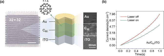
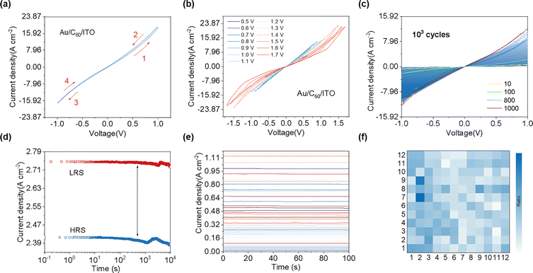
Fig. 1(a) presents the configuration of the fabricated Au/C60/ITO organic memory array. The functional C60 layer was grown on a transparent conductive ITO substrate via vacuum thermal evaporation. Under a high vacuum of 4.4 × 10⁻⁴ Pa, the evaporation source was driven by a DC voltage of 6 V for continuous deposition over 30 min. Subsequently, an Au top electrode was deposited for 50 s at 5 × 10⁻⁴ Pa using a DC voltage of 14 V, yielding dense, continuous metallic coverage with good optoelectronic coupling and conductivity. The upper-left inset image in Fig. 1(a) illustrates a C60 molecule with a diameter of approximately 7.1 Å, emphasizing its molecular-scale and localized-trap characteristics. The right image in Fig. 1(a) shows a cross-sectional FE-SEM image of the Au/C60/ITO multilayer, clearly revealing the layered structure and high-quality interfaces, which underpin the stable resistive switching and photoresponse behavior. Fig. 1(b) characterizes NPM observed under forward bias in the high-resistance state (HRS). Compared with dark conditions, illumination causes a pronounced decrease in current, yielding typical and repeatable NPM. This photo-induced suppression can be attributed to the enhanced capture and recombination of photogenerated carriers in quantized/trap states within the C60 layer, which reduces effective carrier injection and channel transport.Fig. 2 presents the electrical switching behavior of Au/C60/ITO optoelectronic memory. Fig. 2(a) presents the typical bipolar resistive switching characteristics of Au/C60/ITO memory, exhibiting a highly symmetric I–V curve at both voltage polarities, which indicates uniform interfacial properties and balanced charge injection at both electrodes. Building upon this fundamental behavior, Fig. 2(b) demonstrates the analog modulation of conductance states under bias voltages ranging from 0.5 V to 1.7 V, enabling the gradual resistance tuning that is essential for synaptic plasticity. The switching memory behavior is well maintained after experiencing 103 DC voltage sweeps, suggesting that this device has good cycling endurance, as shown in Fig. 2(c). Meanwhile, the HRS and LRS were read at a low disturbance voltage of 0.1 V. The current–time (i–t) curves measured for 104 s at a read voltage of 0.1 V demonstrate that data storage in the RRAM is nonvolatile, as shown in Fig. 2(d). Furthermore, the device's capability for multi-level storage, crucial for neuromorphic computing, is demonstrated in Fig. 2e. By applying successive linear I–V sweeps from 0.5 V to 0.9 V in fine 0.01 V steps, we achieve 32 distinct and stable conductance states. Each state was read at 0.1 V, confirming 5-bit resolution and exceptional analog control, and underscoring the potential for high-precision synaptic applications. Finally, the device-to-device uniformity, depicted in Fig. 2(f), affirms the reproducibility and scalability of the memory architecture, supporting its feasibility for integrated array applications.
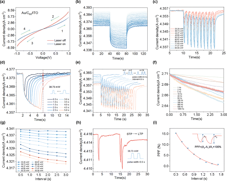
The optoelectronic modulation and synaptic functionality of Au/C60/ITO memory are systematically elucidated in Fig. 3, which progresses from the fundamental photoresponse to multi-parameter synaptic plasticity control. The current–voltage characteristics measured under dark and illuminated conditions reveal the NPM effect, where illumination markedly suppresses the current, consistent with the photon-induced enhancement of carrier trapping or scattering in the active layer (Fig. 3(a)). Building upon this robust NPM behavior, Fig. 3(b) demonstrates photo-modulated synaptic plasticity, with 32 distinct and nearly linear photoconductance states, achieving 5-bit precision via analog weight updates, which is directly relevant for neuromorphic computing. To further clarify the control of optical programming, Fig. 3(c) shows light-power-dependent conductance modulation under pulsed illumination (0.5-s intervals) from 33.2–63 mW, highlighting that increased photon flux enables progressive and controllable conductance transitions. Keeping the illumination power fixed, Fig. 3(d) then shows the effect of the pulse width, underscoring that temporal tuning provides precise control of the charge-trapping kinetics and state evolution. In a complementary manner, Fig. 3(e) investigates the cumulative impact of repeated optical stimuli by varying the number of pulses at constant power, revealing dose-dependent conductance updates that drive reproducible state transitions. In support of dynamic operation, Fig. 3(f) evaluates the frequency response of the photocurrent under 1064 nm illumination from 1 Hz to 1000 Hz, demonstrating a broad spectral response from visible to infrared light and offering insight into device bandwidth and response speed for high-rate optical signaling across a wide spectrum. Extending from single-parameter to coupled control, Fig. 3(g) presents dual-parameter program-mability via simultaneous adjustment of pulse amplitude and width, enabling more flexible and fine-grained synaptic weight regulation. Fig. 3(h) demonstrates the transition from short-term to long-term plasticity (STP-to-LTP) under optical pulses (38.37 mW, 0.4 s), mimicking memory consolidation in biological synapses through the nonvolatile stabilization of photo-programmed states. Complementarily, Fig. 3(i) exhibits paired-pulse facilitation (PPF) using two identical light pulses with inter-pulse intervals ranging from 0.3 to 1.7 s, where the transient response follows an exponential decay function. This temporal filtering behavior, characteristic of biological synapses, underscores the device's capability to encode temporal light information and perform time-dependent signal processing, thereby providing a functional foundation for dynamic vision sensors and photonic spiking neural networks.
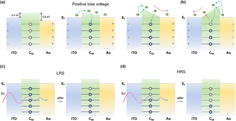
Having characterized the device's electrical and optical performance, we now turn to the underlying physical mechanisms. Fig. 4 elucidates the electric-field-driven and photo-induced charge-trapping mechanisms responsible for the observed resistive switching and negative photoconductance in Au/C60/ITO memory. The energy band alignment is initially governed by work function differences: ΔΦAu–C60 ≈ 0.8 eV and ΔΦC60–ITO ≈ 0.4 eV, facilitating more efficient electron injection from the ITO and C60 sides. The C60 layer contains discrete quantum defect states—schematically represented in Fig. 4(a) by four trap sites.
Under a positive bias at Au and a negative bias at ITO, the energy bands evolve as the applied field increases. In the initial low-bias condition (Fig. 4(a)), the Fermi levels of Au and ITO are not aligned, and only mild band bending occurs in the C60 layer. Electrons from ITO enter the C60 layer primarily through electron transition over the energy barrier, with a negligible contribution from tunneling due to the thick effective barrier resulting from the shallow energy slope. Some of these electrons occupy available quantum defects, while others drift toward the Au electrode. Under intermediate bias, the bands further align, and the Fermi levels equilibrate across the junction. The energy gradient from ITO to Au becomes steeper, reducing the tunneling barrier thickness and enabling a combination of thermionic emission and Fowler–Nordheim tunneling. This enhances electron trapping, partially filling the defect states. Under high bias, strong band bending produces a steep energy slope, favoring efficient tunneling and leading to the complete filling of the four defect states. This trap-filling process corresponds to the ‘write’ operation, transitioning the device to a low-resistance state.
To reset the device, a negative bias is applied to Au and a positive bias to ITO (Fig. 4(b)), reversing the energy slope such that the bands tilt downward from Au to ITO. This promotes electron injection from Au into C60. While some electrons may fill empty shallow traps, the dominant effect is the emptying of the previously occupied defect states due to enhanced detrapping toward ITO under the reversed field. This process constitutes the ‘erase’ operation, restoring the high-resistance state.
Under optical excitation, Fig. 4(c) and (d) illustrate the negative photoconductance mechanism in both low- and high-resistance states. In the LRS (Fig. 4(c)), where more traps are filled (e.g., five occupied sites), photons excite carriers from shallow and deep traps into the conduction band, where they are swept out by the internal field. The resulting increase in empty trap sites enhances scattering and reduces conductivity. Similarly, in the HRS (Fig. 4(d)), with fewer filled traps (e.g., three occupied sites), light-induced detrapping—mainly from shallow states—further depletes trapped charge, also yielding a negative photoconductance response. Thus, both electrical switching and photomodulation operate through the filling and emptying of the same quantum defect states, providing a unified model for the memristive and optoelectronic behavior.
3. Conclusions
In conclusion, we demonstrate a vertical Au/C60/ITO optoelectronic memristor that delivers light-tunable NPM for neuromorphic in-sensor computing. The NPM magnitude and dynamics can be flexibly programmed based on light intensity, pulse width, frequency, and pulse number, enabling up to 32 distinct conductance states and the emulation of STP, LTP, and PPF. A defect-assisted band mechanism links the electrical write/erase process to trap filling/emptying, while photon-assisted trap reconfiguration underlies NPM and memory fading. These results provide a compact, energy-efficient hardware platform with a credible mechanism for use in programmable vision frontends.Conflicts of interest
The authors have no conflicts to disclose.Data availability
The data that support the findings of this study are available from the corresponding author upon reasonable request.Acknowledgements
This work was supported by the Key Project of Chongqing Natural Science Foundation Joint Fund (CSTB2023NSCQ-LZX0103), New Chongqing Youth Innovation Talent Project (Grant No. CSTB2024NSCQ-QCXMX0070), Fundamental Research Funds for the Central Universities (SWUZLPY03), the National Natural Science Foundation of China (Grant Nos U20A20227, 62288102, and 62471251), Basic Research Program of Jiangsu (BK20240033), Fundamental Research Funds for the Central Universities (No. SWUXDZD22009), and the Chongqing Graduate Student Research Innovation Project (CYS25189).References
- S. Y. Wang, X. F. Shi, J. Y. Gong, W. R. Liu, C. X. Jin, J. Sun, Y. Y. Peng and J. L. Yang, Artificial retina based on organic heterojunction transistors for mobile recognition, Nano Lett., 2024, 24, 3204–3212 CrossRef CAS PubMed.
- X. G. Duan, Z. L. Cao, K. K. Gao, W. T. Yan, S. Y. Sun, G. D. Zhou, Z. H. Wu, F. G. Ren and B. Sun, Memristor-based neuromorphic chips, Adv. Mater., 2024, 36, 2310704 CrossRef CAS.
- S. W. Pan, S. Q. Wu, J. Y. Ming and H. F. Ling, Toward energy-efficient machine vision: advances in optoelectronic memristors, Adv. Opt. Mater., 2025, e01992 CrossRef CAS.
- L. X. Hu, J. Yang, J. R. Wang, P. H. Cheng, L. O. Chua and F. Zhuge, Alloptically controlled memristor for optoelectronic neuromorphic computing, Adv. Funct. Mater., 2021, 31, 2005582 CrossRef CAS.
- Y. H. Cao, K. A. Jiang, Y. Y. Zhang, D. H. Huang and H. Wang, Low-voltage driven I-V hysteresis loop in Ag/SrTiO3/Si heterostructure, Appl. Phys. Lett., 2025, 127, 052102 CrossRef CAS.
- H. L. Park, M. H. Kim and S. H. Lee, Introduction of interfacial load polymeric layer to organic flexible memristor for regulating conductive filament growth, Adv. Electron. Mater., 2020, 6, 2000582 CrossRef CAS.
- J. W. Chen, Z. Zhou, B. J. Kim, Y. Zhou, Z. Q. Wang, T. Q. Wan, J. M. Yan, J. F. Kang, J. H. Ahn and Y. Chai, Optoelectronic graded neurons for bioinspired in-sensor motion perception, Nat. Nanotechnol., 2023, 18, 882–888 CrossRef CAS PubMed.
- P. S. Shan, J. Su, Y. Liu, R. W. Wang, M. H. Xu, W. J. Kong, J. H. Zhao and T. Liu, Controlled filament stability in SrTiO3 memristors via swift Xe ion irradiation, Appl. Phys. Lett., 2025, 127(9), 092106 CrossRef CAS.
- Y. Zhang, Z. H. Wu, W. Wu, H. J. Sun, Y. Z. Guo, L. H. Wang, X. M. Zhang, Q. Liu, H. B. Lv, K. H. Xue, G. W. Xu, X. S. Miao, S. B. Long and M. Liu, Evolution of the conductive filament system in HfO2-based memristors observed by direct atomic-scale imaging, Nat. Commun., 2021, 12, 7232 CrossRef CAS.
- C. Worsley, Reactions at the grain surface, Nat. Energy, 2025, 10(9), 1050–1051 CrossRef CAS.
- M. Wang, J. Q. Tu, Z. C. Huang, T. Wang, Z. H. Liu, F. L. Zhang, W. L. Li, K. He, L. Pan, X. M. Zhang, X. Feng, Q. Liu, M. Liu and X. D. Chen, Tactile near-sensor analogue computing for ultrafast responsive artificial skin, Adv. Mater., 2022, 34, 2201962 CrossRef CAS.
- H. Wang, C. Q. Zhang, W. Q. Huang and X. P. Zou, Research progress of ABX3-type lead-free perovskites for optoelectronic applications: materials and devices, Phys. Chem. Chem. Phys., 2022, 24, 27585–27605 RSC.
- M. Yuan, A review of synaptic devices based on organic ferroelectric materials, Phys. Chem. Chem. Phys., 2025, 27, 7502–7518 RSC.
- Z. Liu, S. L. Dai, Y. Wang, B. Yang, D. D. Hao, D. P. Liu, Y. W. Zhao, L. Fang, Q. Q. Ou, S. Jin, J. W. Zhao and J. Huang, Photoresponsive transistors based on lead-free perovskite and carbon nanotubes, Adv. Funct. Mater., 2020, 30, 1906335 CrossRef CAS.
- J. Li, Y. Xin, B. Sun, D. S. Gu, C. R. Liao, X. F. Hu, L. D. Wang, S. K. Duan and G. D. Zhou, Flexible artificial vision computing system based on FeOx optomemristor for speech recognition, J. Semicond., 2025, 46, 012604 CrossRef CAS.
- W. Q. Zhang, B. Gao, J. S. Tang, P. Yao, S. M. Yu, M. F. Chang, H. J. Yoo, H. Qian and H. Q. Wu, Neuro-inspired computing chips, Nat. Electron., 2020, 3, 371–382 CrossRef.
- M. Martemucci, F. Rummens, Y. Malot, T. Hirtzlin, O. Guille, S. Martin, C. Carabasse, A. F. Vincent, S. Saïghi, L. Grenouillet, D. Querlioz and E. Vianello, A ferroelectric–memristor memory for both training and inference, Nat. Electron., 2025, 8(10), 921–933 CrossRef PubMed.
- J. Xu, M. M. Lv, B. Xue and S. N. Tian, A five-terminal ITO transistor enabling memory, artificial synaptic behaviors, and logic operations, J. Chem. Phys., 2025, 162, 224201 CrossRef CAS.
- S. J. Zhao, C. Y. Han, W. H. Liu, P. T. Lai, X. Li, S. Q. Fan, X. L. Wang, J. Hu and L. Geng, Observation of three types of NDR in flexible VOx Mott memristors, Appl. Phys. Lett., 2025, 127, 083502 CrossRef CAS.
- K. S. Woo, J. Han, S. I. Yi, L. Thomas, H. Park, S. Kumar and C. S. Hwang, Tunable stochastic memristors for energy-efficient encryption and computing, Nat. Commun., 2024, 15, 3245 CrossRef CAS PubMed.
- L. Y. Yao, C. Ma, Z. X. He, Y. H. Wang, H. J. Song, X. L. Zhong and J. B. Wang, High-speed Ta2O5-based threshold switching memristor for LIF neurons, J. Appl. Phys., 2025, 136, 144902 CrossRef.
- I. Antonova, V. Seleznev, N. Nebogatikova, A. Ivanov, B. Voloshin and V. Volodin, Thin V2O5 films synthesized by plasma-enhanced atomic layer deposition for memristive applications, Phys. Chem. Chem. Phys., 2023, 25, 32132–32141 RSC.
- G. D. Zhou, B. Sun, X. F. Hu, L. F. Sun, Z. Zou, B. Xiao, W. K. Qiu, B. Wu, J. Li, J. J. Han, L. P. Liao, C. Y. Xu, G. Xiao, L. H. Xiao, J. B. Cheng, S. H. Zheng, L. D. Wang, Q. L. Song and S. K. Duan, Negative photoconductance effect: an extension function of the TiOx-based memristor, Adv. Sci., 2021, 8, 2003765 CrossRef CAS.
- Z. H. Yang, D. S. Gu, B. C. Zhang, P. Li, B. Sun, C. R. Liao, Y. Zhou, J. Yan, X. F. Hu, L. D. Wang, S. K. Duan and G. D. Zhou, Polymer optoelectronic synapse with tunable negative photoconductance memory for sequential signal processing, ACS. Appl. Electron. Mater., 2025, 7(5), 1966–1974 CrossRef CAS.
- Y. J. Liang, F. Zhang, S. Qi, D. M. Dong, X. T. Ma, Y. T. Yang, W. H. Tang, H. Yang and Z. P. Wu, Deep ultraviolet optoelectronic memristors based on gallium oxide for biomimetic visual processing and neuromorphic memory applications, Appl. Phys. Lett., 2025, 126, 141102 CrossRef CAS.
- M. Wang, Z. Yan, T. Wang, P. Q. Cai, S. Y. Gao, Y. Zeng, C. J. Wan, H. Wang, L. Pan, J. C. Yu, S. W. Pan, K. He, J. Lu and X. D. Chen, Gesture recognition using a bioinspired learning architecture that integrates visual data with somatosensory data from stretchable sensors, Nat. Electron., 2020, 3, 563–570 CrossRef.
- L. Zhao, H. Fang, J. Wang, F. Nie, R. Q. Li, Y. L. Wang and L. M. Zheng, Selective and quasi-continuous switching of ferroelectric Chern insulator devices for neuromorphic computing, Nat. Nanotechnol., 2024, 19, 962 CrossRef PubMed.
- E. Baek, T. Rim, J. Schütt, C. K. Baek, K. Kim, L. Baraban and G. Cuniberti, Negative photoconductance in heavily doped Si nanowire field-effect transistors, Nano Lett., 2017, 17, 6727 CrossRef CAS PubMed.
- Z. Y. Li, P. L. Liu, G. H. Yang, C. H. Jia and W. F. Zhang, Tuning bienenstock–cooper–munro learning rules in a two-terminal memristor for neuromorphic computing, Phys. Chem. Chem. Phys., 2023, 25, 15920–15928 RSC.
- (a) B. W. Li, S. Zu, J. D. Zhou, Q. Jiang, B. W. Du, H. Y. Shan, Y. Luo, Z. Liu, X. Zhu and Z. Y. Fang, Single-nanoparticle plasmonic electro-optic modulator based on MoS2 monolayers, ACS Nano, 2017, 11, 9720–9727 CrossRef CAS PubMed; (b) D. Q. Zou, W. K. Zhao, Y. Q. Xu, X. T. Li, Y. L. Liu and C. L. Yang, Dual transmission channels at metal-MoS2/WSe2 hetero-bilayer interfaces, Phys. Chem. Chem. Phys., 2023, 25, 16896–16907 RSC.
- L. Mennel, J. Symonowicz, S. Wachter, D. K. Polyushkin, A. J. Molina-Mendoza and T. Mueller, Ultrafast machine vision with 2D material neural network image sensors, Nature, 2020, 579, 62–66 CrossRef CAS PubMed.
- Y. Chai, In-sensor computing for machine vision, Nature, 2020, 579, 32–33 CrossRef CAS PubMed.
- (a) Y. Wang, E. Liu, A. Gao, T. Cao, M. Long, C. Pan, L. Zhang, J. Zeng, C. Wang, W. Hu, S. J. Liang and F. Miao, Negative photoconductance in van der Waals heterostructure-based floating gate phototransistor, ACS Nano, 2018, 12, 9513 CrossRef CAS PubMed; (b) Y. Zhang, Y. Wang, C. Qin and J. L. Cao, Synthesis and modification of boron nitride nanomaterials for gas sensors: from theory to application, Phys. Chem. Chem. Phys., 2024, 26, 28307–28331 RSC.
- G. D. Zhou, J. Li, Q. L. Song, L. D. Wang, Z. J. Ren, B. Sun, X. F. Hu, W. H. Wang, G. B. Xu, X. D. Chen, L. Cheng, F. C. Zhou and S. K. Duan, Full hardware implementation of neuromorphic visual system based on multimodal optoelectronic resistive memory arrays for versatile image processing, Nat. Commun., 2023, 14, 8489 CrossRef CAS.
- Z. H. Zhang, S. Y. Wang, C. S. Liu, R. Z. Xie, W. D. Hu and P. Zhou, All-in-one two dimensional retinomorphic hardware device for motion detection and recognition, Nat. Nanotechnol., 2022, 17, 27–32 CrossRef CAS.
| This journal is © the Owner Societies 2026 |


