 Open Access Article
A first-principles theoretical study on two-dimensional MX and MX2 metal halides: bandgap engineering, magnetism, and catalytic descriptors
Yu-Hsiu
Lin
 a,
Daniel
Maldonado-Lopez
 a and
Jose L.
Mendoza-Cortes
 *ab
*ab
aDepartment of Chemical Engineering and Materials Science, Michigan State University, East Lansing, MI 48824, USA. E-mail: jmendoza@msu.edu
bDepartment of Physics & Astronomy, Michigan State University, East Lansing, Michigan 48824, USA
First published on 18th December 2025
Abstract
Metal halides, particularly MX and MX2 compounds (where M represents metal elements and X = F, Cl, Br, I), have attracted significant interest due to their diverse electronic and optoelectronic properties. However, a comprehensive understanding of their structural and electronic behavior, particularly the evolution of these properties from bulk to low-dimensional forms, remains limited. To address this gap, we performed first-principles calculations to develop a database of 60 MX and MX2 metal halides, detailing their structural and electronic properties in both bulk and slab configurations. Calculations were performed using the advanced HSE06-D3 hybrid functional for density functional theory (DFT), ensuring high precision in predicting material properties despite the associated computational cost. The results reveal that these materials are predominantly semiconductors, but their bandgaps range from 0 to 9 eV. A detailed analysis of the transition from bulk to slab structures highlights notable shifts in electronic properties, including bandgap modifications. Upon dimensional reduction, 9 materials exhibit an indirect-to-direct bandgap transition, enhancing their potential for energy conversion. Beyond structural dimensionality, the influence of chemical composition on bandgap variations was also examined. To further assess their practical applicability, the catalytic and magnetic properties of these metal halides were systematically evaluated. These findings not only illuminate previously underexplored MX and MX2 metal halides but also identify promising candidates for electronic, optoelectronic, catalytic and spintronic applications. This database serves as a valuable resource for guiding future research and technology development in low-dimensional materials.
1 Introduction
Since the groundbreaking exfoliation of graphene from graphite,1 two-dimensional (2D) materials have become a focal point of research due to their unique properties and potential applications.2–4 These materials often exhibit distinct characteristics compared to their bulk counterparts, making them valuable for various technological applications.5,6 However, the vast diversity of 2D materials has left many of them underexplored. Among these, pristine MX and MX2 metal halides represent a significant yet understudied class of 2D materials, with limited comprehensive experimental and computational investigations.7,8 Previous studies on MX and MX2 metal halides often focus on specific elements or small subsets of the periodic table, leaving a substantial portion of this material class unexplored.9 Despite this, the potential of these materials in applications such as optoelectronics,10–16 spintronics,17–19 thermoelectrics,20 energy storage,21 and magnetism22–26 has been increasingly recognized. In addition, in existing theoretical studies, the accuracy of the prediction still has room for refinement. This highlights the need for a comprehensive and precise database that consolidates the structural and electronic properties of MX and MX2 metal halides.Theoretical studies of metal halides have predominantly employed density functional theory (DFT) with generalized gradient approximation (GGA) functionals, such as PBE, for both geometric optimizations and property calculations.26–28 While these methods offer high computational efficiency, they often yield significant deviations in key properties, such as bandgap underestimation. For example, calculations on monolayer MX2 metal iodides have shown that bandgaps computed using the HSE hybrid functional are 0.33–1.27 eV higher than those obtained with PBE.29 In some studies, hybrid functionals have been employed solely for property calculations, while structural information is derived from GGA-level optimizations.13,16,20,25 However, inaccuracies in GGA-optimized geometries can propagate to electronic property predictions. Specifically, discrepancies in lattice constants between PBE and hybrid functionals have been reported, with average errors of 7.6 pm for PBE compared to 3.5 pm for hybrid functionals.29 These geometric differences, though seemingly minor, can have a noticeable impact on electronic properties, underscoring the importance of using consistent and accurate methods for both geometry and property calculations. In this work, we address these limitations by employing DFT with the HSE06 hybrid functional, supplemented by Grimme's three-body dispersion correction (HSE06-D3), for both structural optimizations and property calculations. This approach ensures a higher level of accuracy in predicting the characteristics of MX and MX2 metal halides, providing reliable data.
The properties of both 2D and bulk structures of MX and MX2 metal halides were systematically calculated, as significant changes in properties between these structural forms can offer valuable insights. Such differences, particularly in electronic properties, highlight the potential to tune the characteristics of the material by varying the number of layers, making dimensional reduction a viable strategy for achieving desirable properties for specific applications. With the high accuracy provided by the HSE06-D3 functional, particular attention was given to identifying shifts in electronic properties during the transition from bulk to slab structures, such as indirect-to-direct bandgap transitions. These findings underscore the potential of MX and MX2 metal halides as candidates for targeted electronic and optoelectronic applications. To further explore other potential applicability, detailed calculations and analyses were conducted to investigate their catalytic and magnetic characteristics from the perspective of dimensionality. In addition, trends and correlations between characteristics within the database were analyzed. For example, the influence of varying atomic numbers of halogens on the properties of MX and MX2 compounds was explored, providing a deeper understanding of the factors governing their behavior. This comprehensive investigation not only addresses existing ambiguities surrounding MX and MX2 metal halides but also contributes valuable data to the broader field of 2D materials, paving the way for further exploration and utilization.
2 Results and discussion
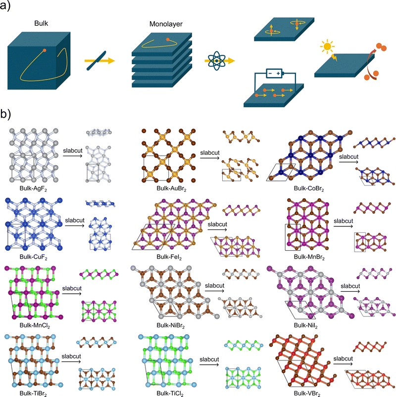
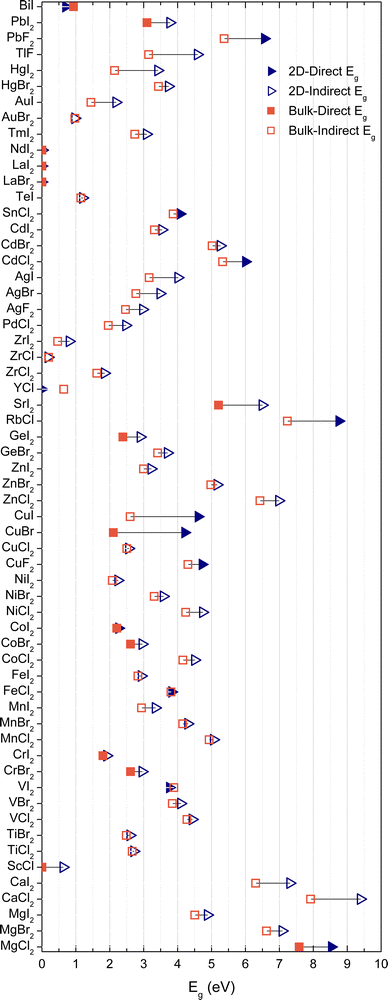
The transformation of bulk materials into isolated 2D monolayers offers a pathway to explore and exploit unique properties that arise from reduced dimensionality. As shown in Fig. 1, the process involves extracting monolayer slabs from bulk structures, followed by ab initio optimization to stabilize their geometry. This dimensional reduction induces significant changes in electronic, catalytic, and spintronic characteristics due to electron confinement effects. The figure also highlights examples of metal halides with optimized bulk and monolayer crystal structures, providing a visual representation of the diversity of materials studied and the atomic compositions involved. These transformations form the foundation for understanding the potential applications of 2D metal halides across various technological domains. Although this work will mainly focus on electronic, optical, catalytic, and magnetic properties, we also analyze the exfoliation energy of our metal halides and—for a subset of these—we verify their stability via vibrational calculations. These analyses can be found in the SI. The relationship between electronic and optical properties is crucial in identifying materials suitable for optoelectronic applications. Leveraging this correlation allows for the efficient screening of candidates from the compiled database. A key example is the conversion of electronic bandgaps into their corresponding wavelengths, as shown in Fig. 2, which illustrates the distribution of bandgaps for the 2D monolayer semiconductors within the database. Among the 60 2D materials analyzed, 57 exhibit nonzero bandgaps, classifying them as semiconductors or insulators, while the remaining materials display metallic behavior. Of the semiconducting materials, 15 possess bandgaps corresponding to wavelengths within the visible (VIS) range, 7 in the infrared (IR), and 35 in the ultraviolet (UV). These findings hold particular significance for applications in energy harvesting, as over 90% of the solar energy reaching Earth's surface consists of visible and infrared light. Materials with direct bandgaps aligned with these wavelengths have the potential to act as efficient solar energy harvesters. Notably, two materials from the database meet these criteria (VIS: CoI2; IR: BiI). While 2D materials with bandgaps in the UV range are less suitable for solar energy applications, they offer promise as UV detectors due to their ability to absorb high-energy photons. Specifically, eleven materials (CdCl2, CoBr2, CuBr, CuF2, CuI, FeCl2, MgCl2, PbF2, RbCl, SnCl2, VI2) were identified with direct bandgaps spanning a broad UV range, from 140 nm to 330 nm. Beyond light absorption, Fig. 2 also provides insights into potential light-emitting applications, offering a preliminary understanding of these materials as emitters at specific wavelengths.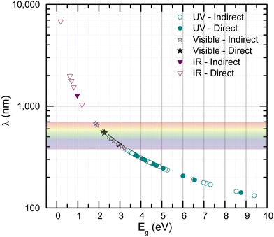 | ||
| Fig. 2 Optoelectronic properties of 2D monolayer semiconductors: solid markers indicate materials with direct bandgaps, while hollow markers denote those with indirect bandgaps. | ||
The exfoliation of graphite into graphene has sparked significant interest in exploring the 2D counterparts of various layered materials. While experimental approaches to synthesizing and characterizing these materials are often labor-intensive and time-consuming, advancements in computational techniques have provided an efficient alternative for predicting and analyzing their properties. Fig. 3 offers computational insights into the potential benefits of exfoliating bulk materials into their 2D forms, focusing on changes in electronic properties. In Fig. 3, the data points represent the bandgap values of both 2D and bulk materials, along with their bandgap types (direct or indirect). Generally, the bandgap tends to increase slightly as the structure transitions from bulk to monolayer. However, four materials (BiI, VI2, YCl, ZrCl) exhibit a notable decrease in bandgap upon this transformation. These findings highlight the potential to fine-tune electronic properties by modulating the number of layers in layered materials. Furthermore, transitions in bandgap types, such as from indirect to direct, are observed, which have significant implications for energy efficiency and optoelectronic applications. Specifically, nine materials (CdCl2, CoBr2, CuF2, CuI, FeCl2, PbF2, RbCl, SnCl2, VI2) undergo an indirect-to-direct bandgap transition during the bulk-to-slab transformation, enhancing their potential for efficient light emission and absorption. Conversely, some materials experience other types of transitions: BiI, CoI2, CuBr, and MgCl2 remain direct bandgaps, LaBr2 and LaI2 keep zero bandgaps, while six others (CrBr2, CrI2, GeI2, NdI2, PbI2, SrI2) exhibit direct-to-indirect transitions. More extremely, ScCl and YCl can shift between a semiconductor and a conductor with a zero bandgap by undergoing the dimensional transformation. These results demonstrate that both the magnitude and type of bandgap are influenced by the number of layers, underscoring the versatility of these materials for tailored applications in electronic and optoelectronic devices. Apart from the bandgap, the crystal structures are affected fundamentally. The mean bond distance between metal and halide atoms is shown in Fig. S2 (see SI), which quantifies how elemental and dimensional factors impact geometry.
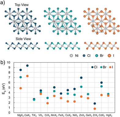
Fig. 4 illustrates the relationship between the bandgaps of MX2 metal halides and the halogen element (X). A general trend emerges in which the bandgap decreases as the atomic number of the halogen increases. This observation is consistent with the differences in electronegativity among halogens (Cl > Br > I). Lower electronegativity weakens the bonding between the metal and halogen atoms, reducing the localization of electronic states and resulting in narrower bandgaps.30 These findings highlight the potential for tuning the electronic properties of metal halides by manipulating the strength and nature of their bonding. Such trends are not unique to the HSE06-D3 calculations used in this study but have also been observed in prior computational works employing GGA and LDA functionals, such as those investigating monolayer alkaline earth and transition metal halides,31 and organometallic halide perovskites.32 This alignment underscores the robustness of the observed trends and provides a qualitative and quantitative framework for understanding the electronic behavior of metal halides.
Fig. 5 presents the band edge alignments relative to the vacuum level for spin-polarized monolayers in the database. The spin-up and spin-down bands are plotted separately, enabling the identification of materials with potential spintronic applications. Specifically, these monolayers exhibit spin-split band structures, where the spin-up and spin-down electrons have distinct bandgap values. Among these monolayers, the MX2 metal halides, in which M = Co, Cu, and Ni, are more likely to induce high spin-polarization. Notably, CrI2 demonstrates characteristics of a half semiconductor. These materials behave as semiconductors (bandgap <3 eV) in a spin channel while acting as insulators (bandgap >3 eV) in the other. This unique behavior arises because of distinct band edges in the two spin channels. Consequently, upon thermal or optical excitation, these materials can generate spin-polarized electrons or holes, a property desirable for spintronic devices. Furthermore, AgF2, CuCl2, and NiI2 stand out as potential bipolar magnetic semiconductors. In these materials, the VBM is fully polarized in the spin-up channel, while the CBM is fully polarized in the spin-down channel. This configuration makes it possible to achieve fully spin-polarized currents by applying an external gate voltage. For example, AgF2 under zero gate voltage behaves as a conventional semiconductor. However, when a negative gate voltage is applied, the Fermi level shifts down, enabling a conductive spin-up electron channel while maintaining a semiconducting spin-down channel. Conversely, a positive gate voltage raises the Fermi level, resulting in a conductive spin-down channel and an insulating spin-up channel. This ability to control spin orientation and polarization through gate voltage modulation positions materials as promising candidates for next-generation spintronic applications. The tunability of spin-dependent electronic properties in these materials highlights their potential for developing efficient and versatile spintronic devices.
The potential catalytic activity of the materials can also be assessed using Fig. 5, which includes energy references for two key catalytic reactions: hydrogen reduction (H+/H2) and oxygen evolution (O2/H2O). These reactions are represented by the standard hydrogen electrode (SHE) and standard oxygen electrode (SOE) energy levels, plotted as blue and red dashed lines, respectively. A semiconductor with a CBM positioned above the SHE level can supply excited electrons with sufficient energy for hydrogen reduction, making it a viable candidate for this reaction. Conversely, a material with a VBM below the SOE level can facilitate oxygen evolution by providing holes at appropriate energy levels. Given the growing demand for sustainable energy solutions, identifying materials capable of catalyzing both hydrogen reduction and oxygen evolution is critical for efficiently producing hydrogen from water. For a material to be classified as a potential water-splitting photocatalyst, it must meet three criteria: (1) the CBM should be above the SHE level to enable hydrogen reduction, (2) the VBM should be below the SOE level to support oxygen evolution, and (3) the bandgap should fall within the main solar spectrum (1.2–2.8 eV) to harness sunlight effectively for charge carrier generation.33 Among these spin-polarized monolayers, two materials satisfy these requirements: CrI2 with a bandgap of 1.91 eV in the α-electron channel and NiI2 with a bandgap of 2.24 eV in the β-electron channel, indicating their potential for photocatalytic applications.
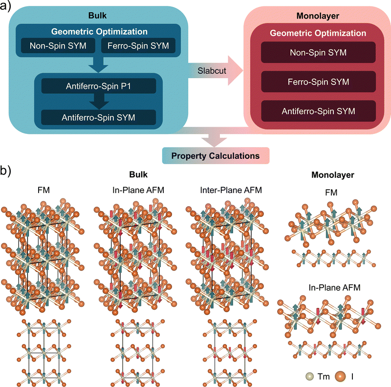
The distribution of spin not only governs the magnetic properties of materials but also plays a critical role in determining their structural stability. To account for this, different initial spin configurations were applied during the design phase prior to geometric optimization. The most stable spin configuration for each material was identified as the one corresponding to the lowest total energy after optimization. To systematically analyze the influence of dimensionality on magnetic properties, the types of magnetism, ferromagnetic (FM) or antiferromagnetic (AFM), were determined for both bulk and 2D monolayer forms. Fig. 6(a) illustrates the methodology used to define the magnetic states of the 60 metal halides. Initially, bulk structures were optimized both with and without assigned spins corresponding to the FM state. The more stable ground state was then selected between these two configurations. For materials that stabilized in the FM state, an additional optimization was performed with spins assigned to an AFM configuration. Since this reassignment disrupted the original symmetry, a re-symmetrization process was applied, mapping the structure onto a different space group. A second round of energy comparisons between FM and AFM states was conducted to determine the final magnetic states of the bulk structures. Subsequently, the most stable bulk structures were cleaved to construct the initial monolayer models. Before optimization, each monolayer was assigned spin configurations corresponding to FM, AFM, and a non-magnetic state. The final magnetic states of the monolayers were determined based on the lowest-energy configuration among these possibilities. The energy difference of material structures with varied spin assignments is plotted in Fig. S3 (see SI). The variation in spin configurations between bulk and monolayer structures further highlights the effects of electron confinement induced by reduced dimensionality. Fig. 6(b) provides a visual representation of the assigned spin states in both bulk and monolayer forms. Notably, inter-plane AFM ordering is exclusively observed in bulk structures, as the interlayer interactions necessary to sustain this configuration are absent in monolayers.
Within the database, 25 metal halides were found to exhibit magnetic behavior, as summarized in Table 1. Among the 25 magnetic materials, 12 retain the same type of magnetism when transitioning from bulk to monolayer structures. Interestingly, 10 materials (AgF2, CoBr2, CoCl2, CrI2, CuCl2, CuF2, NiBr2, NiCl2, NiI2, and YCl) undergo a magnetic transition from antiferromagnetic in the bulk to ferromagnetic in their 2D monolayer form, and one material (VI2) undergoes an opposite ferromagnetic-to-antiferromagnetic transition. In addition, the magnetic feature disappears in two materials (AuBr2 and ScCl) under a bulk-to-2D transformation. This dimensional transition in magnetic behavior aligns with trends observed in experimentally studied metal halides and provides valuable insights into unexplored materials within the database. These findings highlight the potential of 2D metal halides for applications in spintronics and other magnetic technologies, emphasizing the importance of structural dimensions in tailoring magnetic properties.
| Material | Magnetism (bulk) | Magnetism (slab) |
|---|---|---|
| AgF2 | (Inter) AFM | FM |
| AuBr2 | (Inter) AFM | — |
| CoBr2 | (Inter) AFM | FM |
| CoCl2 | (Inter) AFM | FM |
| CoI2 | (Inter) AFM | (In) AFM |
| CrBr2 | (In) AFM | (In) AFM |
| CrI2 | (In) AFM | FM |
| CuCl2 | (Inter) AFM | FM |
| CuF2 | (Inter) AFM | FM |
| FeCl2 | (In) AFM | (In) AFM |
| FeI2 | (In) AFM | (In) AFM |
| MnBr2 | (In) AFM | (In) AFM |
| MnCl2 | (In) AFM | (In) AFM |
| MnI2 | (Inter) AFM | (In) AFM |
| NiBr2 | (Inter) AFM | FM |
| NiCl2 | (Inter) AFM | FM |
| NiI2 | (Inter) AFM | FM |
| ScCl | FM | — |
| TiBr2 | (In) AFM | (In) AFM |
| TiCl2 | (In) AFM | (In) AFM |
| TmI2 | FM | FM |
| VBr2 | (In) AFM | (In) AFM |
| VCl2 | (In) AFM | (In) AFM |
| VI2 | FM | (In) AFM |
| YCl | (Inter) AFM | FM |
3 Methods
The calculations were carried out using unrestricted hybrid DFT with the Heyd–Scuseria–Ernzerhof (HSE06) exchange–correlation functional,34,35 as implemented in the CRYSTAL23 ab initio solid-state chemistry modeling software.36,37 The HSE06 functional was chosen for its proven accuracy in predicting both structural and electronic properties.29 CRYSTAL23 employs Gaussian-type orbitals (GTOs), which facilitate efficient implementation of advanced methods such as hybrid functionals and post-Hartree–Fock approaches. The structural optimizations were performed using triple-zeta with polarization quality (TZVP) Gaussian basis sets for all elements,38 ensuring high precision. Additionally, the Grimme-D3 dispersion correction was incorporated to account for van der Waals interactions.39The initial bulk structures of metal halides were provided by inorganic crystal structure database (ICSD)40 and Heine et al.41 Materials were first optimized in their bulk form using the HSE06 functional. Then, preliminary monolayer structures were derived from these optimized bulk counterparts by cleaving the slabs along the main crystallographic plane. To avoid self-interactions due to periodic boundary conditions, a vacuum of 500 Å was applied in the [001] direction, a default value in CRYSTAL23 for slab calculations. The use of GTOs instead of plane waves mitigates the computational challenges typically associated with adding large vacuum spaces. GTOs are localized and do not extend throughout vacuum, allowing the calculation of large vacuum unit cells without increasing the computational cost. The convergence thresholds of energies were set at 10−7 a.u. for all geometry optimization and single point energy calculations. The reciprocal space was sampled using a Γ-centered Monkhorst–Pack grid with a resolution of approximately 2π × 1/60 Å−1.42 All structures were optimized under full relaxation of cell parameters and atom positions with applicable symmetries found from FINDSYM.43 For frequency calculations at Γ, the single point energy and between-geometry energy thresholds were set to stricter values, at 10−11 a.u., to avoid numerical errors. Furthermore, for the geometry optimizations prior to frequency calculations, the root mean squared (RMS) gradient, maximum gradient, RMS atomic displacements, and maximum atomic displacements were set to 3 × 10⁻⁵ a.u., 4.5 × 10⁻⁵, 1.2 × 10⁻⁴ a.u., and 1.2 × 10⁻⁴ respectively (one order of magnitude stricter than default optimization tolerances). The magnetic properties of the materials were analyzed by initially assigning polarized spin configurations corresponding to ferromagnetic and antiferromagnetic alignments during structural optimization. A material was classified as magnetic if the assigned spin configuration persisted after optimization and resulted in a more stable ground state compared to non-magnetic configurations. The electronic band structures were calculated along k-paths selected based on the crystal symmetry.
Apart from bandgap values, the band alignment relative to vacuum is crucial for determining the practical applications of spin-polarized 2D metal halides. To achieve this, we calculated the work function, defined as the energy difference between an electron at infinity and the Fermi energy level. We adopted a single-point calculation approach, following the CRYSTAL tutorials website,37 as illustrated in Fig. S1 (see SI), to obtain a better description of the electrostatic potential at vacuum. Specifically, two ghost layers providing electronic states were placed above and below the optimized monolayer metal halides to induce nonzero electrostatic potentials at positive and negative values, sufficiently far away from the slab. In this case, the electrostatic potential was measured at 100 a.u. (≈53 Å) from the monolayer. Band alignment was performed by shifting the bands according to the electrostatic potential, with the vacuum energy level set to 0 eV. The separation distance between the monolayers and ghost layers was adjusted for each compound, ensuring an observable but minimal electron population—typically below 0.01—to achieve an accurate vacuum description without compromising the material's electronic structure. The electrostatic potential was determined as the average of the absolute potentials at positive and negative infinity. This approach addresses the limitations of Gaussian-based DFT calculations, which primarily focus on localized electron density around the material structure.
4 Conclusions
This study comprehensively examines the structural, electronic, and magnetic properties of MX and MX2 metal halides in both bulk and 2D forms using high-accuracy hybrid density functional theory (HSE06-D3). Transformations from bulk to monolayer structures were shown to significantly affect material properties, including bandgap values and types, with indirect-to-direct transitions identified in nine compounds. Such findings highlight the potential of these materials for optoelectronic applications, particularly in solar energy harvesting and ultraviolet detection. The study also identifies promising candidates for spintronic and catalytic applications. Materials like AgF2, NiI2 exhibit spin-polarized electronic properties, while CrI2 and NiI2 show potential for photocatalytic water splitting due to their favorable band alignment and bandgap characteristics. Additionally, magnetic behavior analysis revealed dimensionality-driven transitions between antiferromagnetic and ferromagnetic states in select materials, offering insights for spintronic device design. In summary, this work provides a detailed database and theoretical framework for MX and MX2 metal halides, paving the way for experimental validation and future material optimization. These findings underscore the versatility of metal halides for diverse technological applications, from energy harvesting to spintronics.Author contributions
Conceptualization: YL, DML, JLMC. Methodology: YL, DML, JLMC. Software: YL, DML, JLMC. Validation: YL, DML, JLMC. Formal analysis: YL, DML, JLMC. Investigation: YL, DML. Resources: JLMC. Writing – original draft and sketch preparation: YL, JLMC. Writing – review and editing: YL, DML, JLMC. Visualization: YL, DML, JLMC. Supervision: JLMC. Project administration: JLMC. Funding acquisition: JLMC. All authors have read and agreed to the published version of the manuscript.Conflicts of interest
There are no conflicts to declare.Data availability
The data supporting this article have been included as part of the supplementary information (SI). Supplementary information: additional comprehensive plots for band structures; and structural coordinates (CIF) files for optimized 2D and bulk metal halides. See DOI: https://doi.org/10.1039/d5cp03188e.Acknowledgements
D. M.-L. acknowledges funding by the National Science Foundation Graduate Research Fellowship under Grant No. 2235783. This work was supported in part by computational resources and services provided by the Institute for Cyber-Enabled Research at Michigan State University.References
- K. S. Novoselov, A. K. Geim, S. V. Morozov, D.-E. Jiang, Y. Zhang, S. V. Dubonos, I. V. Grigorieva and A. A. Firsov, Science, 2004, 306, 666–669 CrossRef CAS PubMed.
- M. Xu, T. Liang, M. Shi and H. Chen, Chem. Rev., 2013, 113, 3766–3798 CrossRef CAS PubMed.
- Q. H. Wang, K. Kalantar-Zadeh, A. Kis, J. N. Coleman and M. S. Strano, Nat. Nanotechnol., 2012, 7, 699–712 CrossRef CAS PubMed.
- M. Chhowalla, H. S. Shin, G. Eda, L.-J. Li, K. P. Loh and H. Zhang, Nat. Chem., 2013, 5, 263–275 CrossRef PubMed.
- X. Qian, J. Liu, L. Fu and J. Li, Science, 2014, 346, 1344–1347 CrossRef CAS.
- A. Kuc, N. Zibouche and T. Heine, Phys. Rev. B: Condens. Matter Mater. Phys., 2011, 83, 245213 CrossRef.
- V. Nicolosi, M. Chhowalla, M. G. Kanatzidis, M. S. Strano and J. N. Coleman, Science, 2013, 340, 1226419 CrossRef.
- S. Lebègue, T. Björkman, M. Klintenberg, R. M. Nieminen and O. Eriksson, Phys. Rev. X, 2013, 3, 031002 Search PubMed.
- G. Ahmed, A. Dashora, M. Sharma and B. Ahuja, Appl. Radiat. Isot., 2010, 68, 286–292 CrossRef CAS.
- X. Huang, Z. Zhuo, L. Yan, Y. Wang, N. Xu, H.-Z. Song and L. Zhou, J. Phys. Chem. Lett., 2021, 12, 7726–7732 CrossRef CAS.
- L. Yue, W. Jin, A.-J. Mao and X. Kuang, J. Phys. Chem. C, 2021, 125, 12983–12990 CrossRef CAS.
- A. V. Kuklin, L. Gao, H. Zhang and H. Ågren, J. Phys. Chem. Lett., 2020, 11, 9759–9765 CrossRef.
- L. Tao and L. Huang, RSC Adv., 2017, 7, 53653–53657 RSC.
- H. Mahida, A. Patel, D. Singh, Y. Sonvane, P. Thakor and R. Ahuja, Superlattices Microstruct., 2022, 162, 107132 CrossRef.
- D. Hoat, T. V. Vu, M. M. Obeid and H. R. Jappor, Superlattices Microstruct., 2019, 130, 354–360 CrossRef.
- A. O. M. Almayyali, H. O. Muhsen, M. Merdan, M. M. Obeid and H. R. Jappor, Phys. E, 2021, 126, 114487 CrossRef.
- L. Zhou, L. Kou, Y. Sun, C. Felser, F. Hu, G. Shan, S. C. Smith, B. Yan and T. Frauenheim, Nano Lett., 2015, 15, 7867–7872 CrossRef.
- Y. An, H. Wang, J. Liao, Y. Gao, J. Chen, Y. Wu, Y. Li, G. Xu and C. Ma, Phys. E, 2022, 142, 115262 CrossRef.
- X. Li, Z. Zhang, Y. Yao and H. Zhang, 2D Mater., 2018, 5, 045023 CrossRef.
- W.-L. Tao, J.-Q. Lan, C.-E. Hu, X.-R. Chen and H.-Y. Geng, Mater. Sci. Semicond. Process., 2022, 148, 106791 CrossRef.
- Y. Wu, J. Phys.: Conf. Ser., 2021, 012104 Search PubMed.
- J. Luo, G. Xiang, Y. Tang, K. Ou and X. Chen, J. Appl. Phys., 2020, 128, 113901 CrossRef.
- X. Xu, Y. Ma, T. Zhang, C. Lei, B. Huang and Y. Dai, Nanoscale Horiz., 2020, 5, 1386–1393 RSC.
- H. Liu, J.-T. Sun, M. Liu and S. Meng, J. Phys. Chem. Lett., 2018, 9, 6709–6715 CrossRef PubMed.
- C.-S. Liu, X.-L. Yang, J. Liu and X.-J. Ye, J. Phys. Chem. C, 2018, 122, 22137–22142 CrossRef.
- Z. Jiang, P. Wang, J. Xing, X. Jiang and J. Zhao, ACS Appl. Mater. Interfaces, 2018, 10, 39032–39039 CrossRef.
- D. Hoat, T. V. Vu, M. M. Obeid and H. R. Jappor, Chem. Phys., 2019, 527, 110499 CrossRef.
- M. Naseri, D. Hoat, K. Salehi and S. Amirian, J. Mol. Graphics Modell., 2020, 95, 107501 CrossRef PubMed.
- D. Rappoport, N. R. Crawford, F. Furche and K. Burke, Encyclopedia of Inorganic Chemistry, 2006 Search PubMed.
- F. Lu, W. Wang, X. Luo, X. Xie, Y. Cheng, H. Dong, H. Liu and W.-H. Wang, Appl. Phys. Lett., 2016, 108, 132104 CrossRef.
- S.-H. Lin and J.-L. Kuo, Phys. Chem. Chem. Phys., 2014, 16, 20763–20771 RSC.
- I. E. Castelli, J. M. Garca-Lastra, K. S. Thygesen and K. W. Jacobsen, APL Mater., 2014, 2, 081514 CrossRef.
- Q. Yan, J. Yu, S. K. Suram, L. Zhou, A. Shinde, P. F. Newhouse, W. Chen, G. Li, K. A. Persson and J. M. Gregoire, et al. , Proc. Natl. Acad. Sci. U. S. A., 2017, 114, 3040–3043 CrossRef.
- J. Heyd, G. E. Scuseria and M. Ernzerhof, J. Chem. Phys., 2003, 118, 8207–8215 CrossRef.
- A. V. Krukau, O. A. Vydrov, A. F. Izmaylov and G. E. Scuseria, J. Chem. Phys., 2006, 125, 224106 CrossRef.
- A. Erba, J. K. Desmarais, S. Casassa, B. Civalleri, L. Donà, I. J. Bush, B. Searle, L. Maschio, L. Edith-Daga and A. Cossard, et al. , J. Chem. Theory Comput., 2022, 19, 6891–6932 CrossRef.
- R. Dovesi, V. Saunders, C. Roetti, R. Orlando, C. Zicovich-Wilson, F. Pascale, B. Civalleri, K. Doll, N. Harrison and I. Bushet al., CRYSTAL23 User’s Manual, University of Torino, Torino, Italy, 2023 Search PubMed.
- D. Vilela Oliveira, J. Laun, M. F. Peintinger and T. Bredow, J. Comput. Chem., 2019, 40, 2364–2376 CrossRef PubMed.
- S. Grimme, J. Antony, S. Ehrlich and H. Krieg, J. Chem. Phys., 2010, 132, 154104 CrossRef PubMed.
- A. Belsky, M. Hellenbrandt, V. L. Karen and P. Luksch, Acta Crystallogr., Sect. B: Struct. Sci., 2002, 58, 364–369 CrossRef PubMed.
- P. Miró, M. Audiffred and T. Heine, Chem. Soc. Rev., 2014, 43, 6537–6554 RSC.
- H. J. Monkhorst and J. D. Pack, Phys. Rev. B, 1976, 13, 5188 CrossRef.
- H. T. Stokes and D. M. Hatch, J. Appl. Crystallogr., 2005, 38, 237–238 CrossRef.
| This journal is © the Owner Societies 2026 |


