
 Open Access Article
 This Open Access Article is licensed under a Creative Commons Attribution-Non Commercial 3.0 Unported Licence
Experimental demonstration of in-memory computing using pressure stimulated SnO2−x-based memristive device as inverter and active-low 2![[thin space (1/6-em)]](https://www.rsc.org/images/entities/h2_char_2009.gif) :1 multiplexer†
:1 multiplexer†
Bishal Kumar
Keshari
 a,
Soumi
Saha
a,
Sanghamitra
DebRoy
b,
Akshay
Salimath
b,
Venkat
Mattela
c,
Subhradeep
Pal
a,
Surya
Shankar Dan
a and
Parikshit
Sahatiya
*a
a,
Soumi
Saha
a,
Sanghamitra
DebRoy
b,
Akshay
Salimath
b,
Venkat
Mattela
c,
Subhradeep
Pal
a,
Surya
Shankar Dan
a and
Parikshit
Sahatiya
*a
aDepartment of Electrical and Electronics Engineering, Birla Institute of Technology and Science (BITS) Pilani, Hyderabad Campus, 500078, India. E-mail: parikshit@hyderabad.bits-pilani.ac.in
bNanomagnetic Division, Ceremorphic India Pvt Ltd, India
cCeremorphic, Inc., San Jose, California 95131, USA
First published on 26th June 2025
Abstract
This article reports a tin oxide (SnO2−x) based memristor. In the Ag/SnO2−x/ITO structured two-terminal memristive device, the silver (Ag) serves as the top electrode (TE), while indium tin oxide (ITO) is used as the bottom electrode (BE), whereas SnO2−x acts as the resistive switching layer. The device demonstrates non-volatile resistive switching (RS) characteristics, with resistance windows of the order of 105 Ω and 104 Ω for electrical and pressure conditions, respectively, maintained up to 11 × 103 switching cycles. The fabricated device's experimentally verified pressure-dependent resistive switching property makes it a potential candidate for human-inspired next-generation artificial intelligence (AI) systems with high power efficiency (0.38 mW in this study). This study reports an integrated digital memory and analog sensor by the fabricated Ag/SnO2−x/ITO memristor in its operation, where utilizing external mechanical pressure and applied voltage as inputs, the output current change makes the device perform as a chip-enabler logic inverter and an active-low 2![[thin space (1/6-em)]](https://www.rsc.org/images/entities/char_2009.gif) :1 multiplexer. This makes the device a “memlogic device” which can be utilised in “in-memory computing” applications, simplifying the next-generation reconfigurable piezoelectric circuits for future AI technology.
:1 multiplexer. This makes the device a “memlogic device” which can be utilised in “in-memory computing” applications, simplifying the next-generation reconfigurable piezoelectric circuits for future AI technology.
1. Introduction
Memristors have found their potential applications in non-volatile memories1 and neuromorphic computing in recent decades.2 The simple MIM (metal–insulator–metal) structures, power efficiency, CMOS compatibility, and the high scalability of metal-oxide-based memristive devices make it promising to shape the landscape of future electronics.3,4 Transition metal oxides (TMOs) such as HfOx, TiOx, TaOx, AlOx, and CuOx are a few of the most studied materials for their resistive switching behavior.1,5 These materials exhibit resistive switching behavior due to the controlled transport of metal cations and/or oxygen vacancies.3 Furthermore, by tuning the Schottky barrier height between the metal and insulating layer, the device's conductivity can be tuned between the HRS (high resistance state) and LRS (low resistance state) or vice versa, under the influence of applied external biases.6 The memristive device is said to be in a ‘SET’ state when it switches from HRS to LRS, while switching back to HRS from LRS, it is said to be in a ‘RESET’ state. Among metal oxides, tin oxide (SnO2) has gained the attention of researchers due to its unique properties in oxide electronics. It is a natively n-type wide band-gap (3.6 eV) semiconductor that is abundant and low-cost.7 These features make SnO2 desirable for optoelectronic devices such as solar cells7 and sensors.8 It has also been successfully demonstrated to behave as an artificial synapse6 and RRAM (Resistive Random Access Memory) device8 based on its reversible resistive switching ability. Hence, tin oxide material can be considered a potential contender for future neuromorphic computing and non-volatile memory based applications.Among all the previously reported synthesis methods,9 hydrothermal synthesis is preferred, as it does not require harsh synthesis conditions, consumes less energy, and produces a homogeneous synthesis of tin oxide using basic equipment without requiring much specialised equipment.8 A low-temperature (160 °C) hydrothermally synthesised SnO2 nanorods was reported by Guo et al.,10 where this method requires approximately 12 h. Anuchai et al. reported one-step hydrothermally synthesised tin oxide (SnO2−x) nanocrystals with oxygen deficiency, which improved the material's photocatalytic performance.11 Zhang et al. reported that the presence of oxygen vacancies in the tin oxide nanocrystals has improved the Ethanol gas sensing ability.12 In the case of valence change mechanism (VCM)-type memristive devices, the presence of oxygen vacancies helps to achieve the forming-free and gradual switching13 memristive behaviours, which are desirable for neuromorphic computing applications.14 Owing to its semiconducting properties, the SnO2 material has been extensively explored for its gas sensing,15–17 optical light sensing,18–20 and memristive applications.7,8 However, the pressure-sensing ability of SnO2 material21 is much less explored or reported.
Hence, the present study is intended to employ tin oxide material with similar characteristics related to sensing, memory and resistive switching22–24 along with the cost-effective and low energy hydrothermal method for possible in-memory computing applications. The crystallographic structure and oxidation states of the grown tin oxide layer were investigated by the XRD (X-ray diffraction) and XPS (X-ray photoelectron spectroscopy) methods, respectively. The UPS (ultraviolet photoelectron spectroscopy) technique was utilized to obtain the work function value of the tin oxide (SnO2−x) layer. The thickness and the surface morphology of the SnO2−x layer were assessed by the SEM (scanning electron microscopy) characterization. Using the synthesised SnO2−x material, an Ag/SnO2−x/ITO device with memristive properties has been fabricated. A physical explanation of the conduction mechanism and resistive switching behavior exhibited by the device is also proposed. Utilising the memristive characteristics of the fabricated device and its response to externally applied mechanical pressure dependent change in the resistance state where the reducing LRS was examined under the application of pressure up to 1.928 kPa; leads to the implementation of logical ‘NOT’ and active low 2:1 multiplexer (MUX), which finds its potential in-memory computing applications for future peizoelectronics and next-generation programmable logic circuits.
2. Result and discussion
2.1 Material characterization
The obtained XRD spectra of the synthesized SnO2−x film (Fig. 1(a)) confirm the presence of SnO2 peaks at 26.8° and 54.8° corresponding to (110) and (220) planes respectively. Where the prominent peak is at 2θ = 26.8°. Cassiterite crystals with rutile-tetragonal structures (JCPDS 41-1445) dominate these peaks.25 The SnO2−x nanoparticle's crystallite size (D) was determined by the Debye–Scherrer relation (Eqn 1): | (1) |
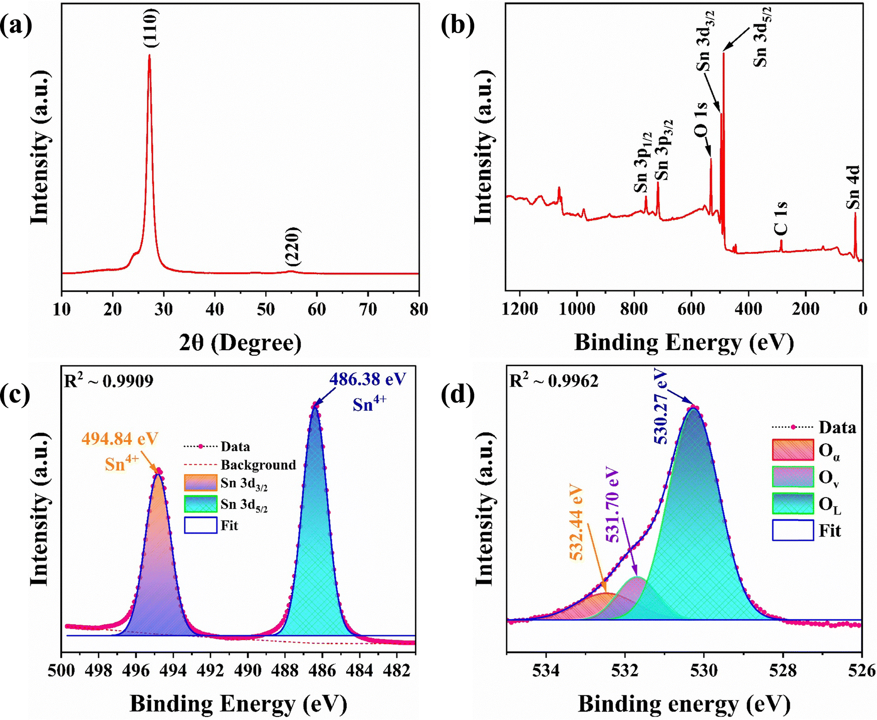 | ||
| Fig. 1 (a) XRD spectra of tin oxide (SnO2−x) film, synthesized by the hydrothermal method. (b) X-ray photoelectron spectroscopy (XPS) survey spectra of SnO2−x spin-coated film, (c) and (d) deconvoluted XPS spectra of Sn 3d and O 1s peaks in SnO2−x film, respectively. | ||
X-ray photoelectron spectroscopy (XPS) study of the fresh surface of tin oxide film was utilized to examine the elements and compositional identification of tin oxide material grown by the hydrothermal method. Fig. 1(b) depicting the XPS survey spectrum of the tin oxide film, confirms the existence of O and Sn elements. Fig. 1(c) and (d) show the deconvoluted XPS spectra of Sn 3d and O 1s peaks of SnO2−x film. As shown in Fig. 1(c), the ascribed binding energies (BEs) associated with Sn 3d3/2 and Sn 3d5/2 peaks are ∼494.84 eV and ∼486.38 eV, respectively. The difference of about 8.46 eV between the two 3d peaks confirms the presence of Sn in the form of Sn4+.7Fig. 1(d) shows the deconvoluted core level fitted O 1s spectra of the SnO2−x layer having three prominent Gaussian subpeaks centered at ∼530.27 eV, ∼531.70 eV and ∼532.44 eV BEs, which corresponds to lattice oxygen (OL) bound to Sn4+, oxygen vacancy (Ov), and adsorbed oxygen or –OH molecules (Oα) bound to the SnO2−x surface in the oxygen deficient sites, respectively.17,26–28 Based on the deconvoluted spectra, the relative percentage of oxygen vacancy was calculated to be 12.31%. This indicates that the active layer comprises a large concentration of oxygen vacancies, hence termed SnO2−x. The significant presence of oxygen vacancies is likely to play a crucial role in the device's resistive switching behavior. Further, the atomic percentages of Sn and O were measured using the energy dispersive spectroscopy (EDS) technique, wherein the values had a strong consistency with the XPS results. The detailed schematic of the tin oxide material synthesis procedure and Ag/SnO2−x/ITO structured device fabrication is illustrated in Fig. S1, ESI.† Also, the EDS study has been discussed under Fig. S2(a–c), ESI.†
The surface morphology of the spin-coated SnO2−x film was examined by the FESEM (field emission scanning electron microscopy) method. Fig. 2(a) depicts the FESEM image of the spin-coated SnO2−x film's surface. Fig. 2(a) shows a homogeneous distribution of the SnO2−x crystallites even at 500 nm scale, which supports the reliability of the fabricated device. Also, using the cross-sectional SEM study at 90° tilt angle, the estimated thickness of SnO2−x film was found to be ∼13 μm (Fig. 2(b)).
 | ||
| Fig. 2 (a) FESEM image of SnO2−x film spin-coated over ITO, (b) cross-sectional FESEM image of SnO2−x and ITO/PET interface at 90° tilt angle. | ||
The energy band gap (Eg) and the work function (Φ) of the SnO2−x film were extracted utilizing the UV-visible (Taucs plot) and ultraviolet photoelectron spectroscopy (UPS) methods, respectively. The measured value of the work function of the SnO2−x layer was estimated to be ∼4 eV, as shown in Fig. 3(a), and the estimated value of the corresponding band gap, ∼3.63 eV, shown in the inset of Fig. 3(a), is consistent with the literature.8 The values of the work functions of Ag and ITO ∼4.7 and ∼4.8 eV, respectively, were taken from the literature.29 Based on the work function and band gap of the fabricated Ag/SnO2−x/ITO memristive device, a schematic energy band diagram of the device is shown in Fig. 3(b).
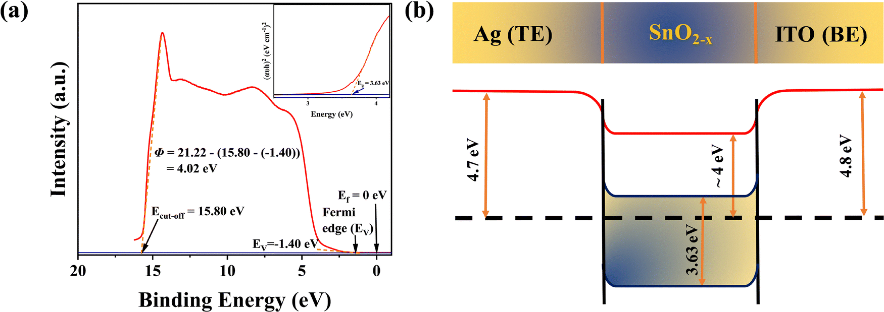 | ||
| Fig. 3 (a) Work function and band gap estimation of SnO2−x film using UPS result and Taucs plot (inset) respectively, (b) band diagram of Ag/SnO2−x/ITO memristive device under equilibrium. | ||
2.2. Electrical characterization
For the current–voltage (I–V) measurements of the fabricated Ag/SnO2−x/ITO device under ambient conditions at room temperature, Keithley 2450 source meter and a DC probe station were utilized. The schematic of the electrical measurement setup of the device is shown in Fig. 4(a), where a DC voltage sweep cycle 0 V → +2 V → 0 V → −2 V → 0 V was applied to the top Ag electrode with bottom ITO electrode grounded, where the compliance current (Icc) was set at 10 mA. Fig. 4(b) demonstrates an asymmetric rectifying bipolar resistive switching behaviour of a pristine Ag/SnO2−x/ITO memristive device. The asymmetric and rectifying I–V characteristics behavior of Ag/SnO2−x/ITO memristive device can be attributed to the presence of asymmetric Schottky barriers (as work function of Ag, SnO2−x, ITO are 4.7 eV, ∼4 eV, and 4.8 eV respectively.) at both Ag/SnO2−x and SnO2−x/ITO interfaces under equilibrium condition, in addition, the oxygen vacancy led conductive path/s formation and dissolution under the applied electric field (details discussed in Fig. S3, ESI†) might have played jointly in achieving the observed I–V characteristics. The fabricated Ag/SnO2−x/ITO is a forming-free memristive device, evident from its DC I–V characteristics, as very less variation in the SET and RESET voltages can be observed in subsequent cycles, as shown in Fig. 4(c).30 The obtained characteristics of the device show that the pristine device was initially at HRS. When the voltage sweep from 0 V → +2 V is applied, the device gradually switches to the LRS at around 1.85 V. The device maintains this LRS until the voltage sweep of opposite polarity (0 V → −2 V) is applied, which is evident from its rectifying nature. Hence, the device RESETs during the negative voltage sweep, exhibiting bipolar resistive switching phenomena.31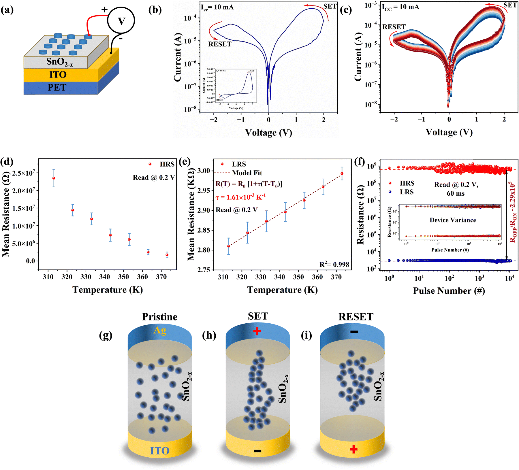 | ||
| Fig. 4 (a) Schematic representation of the electrical measurement setup of the Ag/SnO2−x/ITO device, (b) I–V characteristics of the Ag/SnO2−x/ITO device on the semilog scale (inset: Linear scale), (c) 100-cycle DC IV characteristics of Ag/SnO2−x/ITO memristive device showing analog SET and RESET behavior. Temperature-dependent resistance variation under (d) HRS and (e) LRS. (f) Pulse endurance characteristics of the Ag/SnO2−x/ITO memristive device up to 11 × 103 at room temperature. The inset exhibits switching cycle results obtained for ten different devices for 1 × 10³ switching cycles. Statistical analysis on device-to-device and cycle-to-cycle variation is shown in Fig. S5(a) and S6(a)–(j), ESI.† Schematic illustration of oxygen vacancy-based resistive switching mechanism in the fabricated Ag/SnO2−x/ITO memristive device from (g) pristine state to (h) LRS or SET when Ag TE was positively biased to (i) HRS or RESET when Ag TE was negatively biased under the applied voltage sweep. | ||
It is to be noted that the device shows a gradual increment and decrement in current or analog switching with subsequent voltage sweep cycles and polarities, respectively, as shown in Fig. 4(c). This indicates that metal cation-based conductive-bridge phenomena do not dominate the conduction mechanism, but rather oxygen vacancies.32 Due to the large concentration of oxygen vacancies in the SnO2−x active layer, it may dominate the conduction mechanism in the fabricated device. Therefore, to investigate the nature of conduction and to understand the analog resistive switching characteristics of the fabricated device, a temperature-dependent electrical study was carried out on ten different devices, where temperature-dependent variation in device resistance under the HRS and LRS was recorded at a read voltage of 0.2 V. As shown in Fig. 4(d) the mean resistance of all tested devices under the HRS was found to drop exponentially under the incremental temperature change, ranging 313–373 K. This drop in resistance as a function of increasing temperature attributes to the semiconducting nature of the device under the HRS. On the other hand, Fig. 4(e) shows a linear rise in the mean resistance of all devices under the LRS for incremental temperature change in the range of 313–373 K, which indicates ohmic conduction under the LRS. The temperature-dependent variation in resistance under the LRS in the present case can be expressed as R(T) = R0 [1 + τ(T − T0)], where R(T) is the resistance at the applied temperature T, R0 is the resistance at temperature T0, and τ is the temperature coefficient of resistance. The value of ‘τ’ depends on the nature of the conductive path (ionic or metallic) between the top and bottom electrodes of the device. In case of oxygen vacancy-based conductive path/s formed, the τ's value would range ∼1 × 10⁻³ K−1 to ∼2 × 10⁻³ K−1, whereas, if the conductive path is metallic in nature, then it will lead to a higher value of τ, which lies in the range of ∼3.3 × 10⁻³ K−1 to 4 × 10⁻³ K−1.33,34 By considering T0 as 313 K, the extracted value of τ through the linear fitting of the temperature-dependent resistance plot under the LRS is 1.61 × 10⁻³ K−1. The extracted value of τ is consistent with the previously reported values of temperature coefficient of resistance in the case of oxygen-vacancy-based conductive path/s in memristive devices.34,35 Therefore, as per the experimental results, it can be confirmed that the conductive path/s associated with the Ag/SnO2−x/ITO memristive device's conduction are composed of the oxygen vacancies and not due to the Ag metal cations generated by the oxidation of the Ag top electrode which eventually forms a metallic conductive filament under the applied voltage signals. This experimental analysis is also consistent with previously reported studies, which report strongly restricted migration of Ag metal cations by/through the tin-oxide layer.36,37 Therefore, it can be concluded that the observed analog switching behavior of the device is controlled by the presence of oxygen vacancies in the SnO2−x active layer. The pulse endurance characteristic of the Ag/SnO2−x/ITO memristive device is shown in Fig. 4(f). The pulse scheme applied to the device and the measured current response at 0.2 V/60 ms, under no pressure conditions, are shown in Fig. S4(a), ESI.† Under the applied pulse scheme, the device successfully exhibited repeatable bipolar resistive switching characteristics for 11 × 103 switching cycles, maintaining a resistance window of 2.29 × 10⁵, measured between the mean values (dashed lines in Fig. 4(f)) of HRS and LRS data points. Further, to access the cycle-to-cycle and device-to-device variability, identical pulse schemes were applied to ten different devices for 1 × 10³ switching cycles, where it shows minimal spatial variation as can be observed through the inset of Fig. 4(f), without any significant variations in the order of the resistance window and mean differential low-resistance conductance of each device (read at 0.2 V/60 ms) as shown in Fig. S5(a) and S6(a–j), ESI,† respectively. Hence indicates high uniformity and reliability of the fabricated Ag/SnO2−x/ITO memristive devices. Now, as shown in Fig. 3(b), the SnO2−x layer forms Schottky contacts with the Ag and ITO electrodes. However, based on the work function difference, there is a smaller Schottky barrier at the Ag/SnO2−x interface than that of the SnO2−x/ITO interface. These Schottky barriers control the electron transport during the voltage sweeps. During the positive voltage sweep, i.e. 0 V → 2 V, when Ag TE is positively biased, more number of electrons will accumulate near the Ag/SnO2−x interface, reducing the barrier height at the interface, which will facilitate the easier flow of electrons across the interface. Simultaneously, the randomly distributed oxygen vacancies (Ov) in the pristine device, as illustrated in Fig. 4(g), being charge trapping centres, will drive towards the ITO BE under the influence of applied electric field when Ag TE was positively biased as shown in Fig. 4(h), which helps in forming conductive path/s during the subsequent voltage sweeps.38–40 This makes the device switch to the LRS from HRS. The formation of oxygen vacancy-led conductive path/s during the positive voltage sweep, i.e. 0 V → 2 V, facilitates the flow of electrons and thereby plays a vital role in current conduction in the device. Due to the formed conductive path/s, this state is retained during the backward sweep, i.e., 2 V → 0 V. This state of the device sustains until the negative voltage sweep is applied. Now, as soon as the negative voltage sweep, i.e. 0 V → −2 V, was applied to the device, there could be the dissolution of the conductive path due to the migration of oxygen vacancies in the opposite direction, and the conductive path is likely to be detached from the ITO BE, as shown in Fig. 4(i).41,42 Also, the Schottky barrier height at the Ag/SnO2−x interface will increase, hindering the flow of electrons across this interface. Although the Schottky barrier height at the SnO2−x/ITO interface will reduce under this negative voltage sweep, the dissolution of the oxygen vacancy-led conductive path/s during the negative voltage sweep leads the device to enter HRS from LRS (RESET).39,40 It is to be noted that the reduced Schottky barrier height at the SnO2−x/ITO interface would still be larger than that of the reduced Schottky barrier height at Ag/SnO2−x interface under the same electric field due to the higher work function of ITO than that of Ag, thus also responsible for reduced current during the negative voltage sweep.
 | ||
| Fig. 5 (a) Schematic of PDMS encapsulated Ag/SnO2−x/ITO memristive device for pressure dependent electrical behaviour measurement, (b) I–V characteristics of the Ag/SnO2−x/ITO memristive device under without pressure and with pressure conditions, (c) the temporal response of the Ag/SnO2−x/ITO memristive device with respect to pressure range of 1.249–1.928 kPa, (d) double-log-fitted positive cycle I–V behaviour of Ag/SnO2−x/ITO memristive device under without pressure and 1.249 kPa pressure conditions, (e) Double-log-fitted negative cycle I–V behaviour of Ag/SnO2−x/ITO memristive device under without pressure and 1.249 kPa pressure conditions. (f) Pulse endurance characteristics of the PDMS encapsulated Ag/SnO2−x/ITO memristive device up to 11 × 103 switching cycles under 1.249 kPa, 1.472 kPa and 1.928 kPa pressure conditions, respectively. | ||
The pressure-induced current decrement in the fabricated device can be attributed to more than one reason. The primary reason for this current decrement can be attributed to the disruption of the conductive path/s or a possible change in their morphology under the applied pressure, which leads to the current decrement.49 And the observed attenuated current level during the no-pressure duration can be attributed to the slow transient redistribution of oxygen vacancies-based conductive path/s over the given period of relaxation time. When the device under test was allowed for a longer duration (∼10 minutes) of relaxation time under the constant bias of 2 V, the device got preconditioned to its LRS before changing the amplitude of the applied pressure to the device under test. This preconditioning of the device resulted in almost similar initial current levels for all different applied pressure conditions, as shown in Fig. 5(c). Such pressure-dependent reversible current suppression phenomenon has been reported, including for metal oxides.50,51 Moreover, the grain boundaries of the non-stoichiometric tin oxide (SnO2−x) nanoparticles, as confirmed by the FESEM image (Fig. 2(a)) under the pressure conditions, will move closer to each other, but this increased density of grain boundaries can act as a barrier to the flow of charge carriers.52 In addition, the oxygen vacancies are positively charged,40 and as electron donors53 it can be inferred that they may donate quasi free electrons54 under the applied pressure condition as a function of pressure amplitude, which may enhance the scattering events in the tin oxide layer and along with the grain boundary barriers it helps reducing the electron mobility.
The marginal decrement in current (A1 < A2 < A3 < A4 < A5) under the applied (ON) pressures shows its transition from LTM (long term memory) to STM (short term memory) as shown in Fig. 5(c). The marginal decrement in current with repeated ON pressure, keeping the device under a 2 V bias supply, can be attributed to the collective influence of the pressure amplitude-dependent disruption of conductive path/s along the SnO2−x material stack, reduced mobility due to enhanced scattering events and the grain boundary barrier, as discussed above. When the bias voltage was applied, it led to the formation of oxygen vacancy-led conductive path/s in which disruption is supposed to happen under the applied pressure. It is anticipated that the disruption in conductive path/s does not entirely recover under the given relaxation time (pressure OFF condition for 30 s) while recording the temporal response of the device under applied mechanical pressure, resulting in an increased resistance state of the device. This increased resistance state did not allow the current to return to its original state until a preconditioning step (as mentioned above) was performed. Therefore, it shows that the change in the resistance state that occurs during the applied pressure condition retains even after the pressure is removed.
To further understand the underlying nature of current conduction in the fabricated device within different applied voltage sweep regimes, the DC I–V characteristics of the fabricated Ag/SnO2−x/ITO device without and with pressure conditions are plotted on the logarithmic scales for both positive and negative cycles in Fig. 5(d) and (e), respectively. During the positive forward voltage sweep cycle at lower voltage regime (ln(V) < 0.5 V), ohmic conduction prevails as slope (α)∼1, which indicates thermally generated free carriers.55 After ln(V) = 0.5 V in both the cases of without pressure and 1.249 kPa pressure the I–V characteristics shows space charge limited current (SCLC)56,57 as α ∼ 2 and then trap charge limited current (TCLC) as α is much greater than 2. In absence of pressure, α rapidly increases to 6 and then 18. This indicates the rapid filling of oxygen vacancies with the injected electrons from the ITO electrode and the device turned on. Application of pressure clearly decreases the slope α as compared to without pressure, i.e. 4 and then 11, indicating that under the pressure, the carrier conduction has been disrupted, considerably decreasing current. The α ∼ 2.8 and 2.5 during the backward positive voltage sweep (−0.47 < ln(V) < 0.032) indicates that, once the traps are filled with the injected electrons further injection of the same leads to space charge limited conduction.52,53 During the further backwards positive voltage sweep after the turn ON, it can be observed that the device again shows ohmic behaviour as α ∼ 1.4 for both the conditions, which is also consistent with the temperature-dependent resistance variation study under the LRS. Similarly, the same discussion holds for the negative voltage sweep cycle as shown in Fig. 5(e). The conduction of the device for other pressure conditions (i.e. for 1.478 kPa and 1.928 kPa) was also examined by similar double logarithmic fittings of their corresponding I–V behaviour, which exhibited no significant change in the type of conduction mechanism under each voltage regime. The fitted double logarithmic I–V characteristics corresponding to 1.478 kPa and 1.928 kPa pressure conditions are shown in Fig. S9, ESI.† The pulse endurance characteristics of the device under 1.249 kPa, 1.472 kPa, and 1.928 kPa pressure conditions, maintaining their corresponding resistance states, are shown in Fig. 5(f). The pulse scheme applied to the device and the measured current response under 1.249 kPa, 1.472 kPa, and 1.928 kPa pressure conditions are shown in Fig. S4(b), ESI.† Under the applied pulse scheme, as shown in Fig. S4(b), the device exhibited repeatable bipolar resistive switching characteristics for 11 × 103 switching cycles without fail under different constant pressure conditions, as shown in Fig. 5(f). The PDMS encapsulated Ag/SnO2−x/ITO memristive device shows distinguishable mean resistance states for both HRS and LRS data points, having resistance window values of 8.87 × 10⁴, 5.78 × 10⁴, 4.44 × 10⁴, for 1.249 kPa, 1.427 kPa, 1.928 kPa pressure conditions respectively, measured between their respective mean values (dashed lines in Fig. 5(f)) of HRS and LRS states’. The variations in the HRS and LRS data points around their respective mean values, as shown in Fig. 5(f) and 4(f), can be attributed to the involved stochasticity in the formation and dissolution of oxygen vacancy-based conductive path/s during the SET and RESET operations, respectively.58,59
3. Memlogic applications with pressure input
Memlogic, a memory logic device, has been further investigated in the presence of two different types of signals: one is voltage other is pressure as inputs, and current as output. In this context, pressure and voltage are used as the two input variables for executing Boolean logic operations using the fabricated memristor. In this experiment by applying a negative voltage sweep (0 V → −2 V → 0 V) to the device the current response (absolute value) under without pressure and with varying pressure conditions was observed. The results demonstrate that the applied pressure decreases the output current level. The I–V characteristics of the fabricated memristor under without pressure and with pressure conditions during the negative voltage sweep is shown in Fig. 6(a). The ratio of currents under without pressure and with pressure (1.928 kPa) conditions is determined to be 3.4 × 10². To investigate the memlogic capability of the device a 1.928 kPa of pressure input was induced on the device in every 2 seconds repeatedly, and a negative voltage pulse with amplitude −1 V and duration 1 second was also applied. Fig. 6(b) demonstrates the output current variation with time, where the resultant current is a function of both applied pressure and electrical impulses. A 10 μA of threshold current value was set to distinguish between the OFF and ON states of the device. In case when the output current level exceeds this threshold value, the device is considered ON or in logic HIGH (‘1’) state; otherwise, OFF or in logic LOW (‘0’) state as depicted in Fig. 6(c). Based on this behaviour of the device under different levels of applied voltage and pressure the resultant output current values and associated logic states are compiled as a truth table (Table 1). Based on the truth table it is evident that the device functions as a chip-enabled inverter gate when the read voltage is set at −1 V. | ||
| Fig. 6 (a) Memristive switching of the fabricated device Ag/SnO2−x/ITO without pressure (black) and with pressure (green). (b) Output current level variations without and with pressure conditions under reset electrical logic inputs (read voltage at −1 V) with threshold current 10 μA. (c) Exhibition of memlogic with reprogrammable electrical (current) outputs under various combinations of the electrical and pressure inputs. | ||

|
For the chip-enabled inverter implementation, pressure is used as an input, and voltage is used as an enabler as summarized in Table 1. The following technical observations were made:
1. When the currents are 1.1 μA or 0.14 μA, the resistance offered by the memristor is in the order of MΩ, which we can envisage as a high impedance state ‘Z’. Thus, the logic gate is in a high impedance state when V = 0, irrespective of the pressure input signal.
2. When V = 1, when pressure input P = 0, the current output signal I = 1 while for V = 1 and P = 1, I = 0.
Based on the experimental observations it can be concluded that the fabricated memristor, with the applied pressure operation, functions as a chip-enabler NOT gate, as shown in Fig. 7(a) and (b). Applied pressure alters the mobility of charge carriers within the active layer which as a result aids to the resistive switching. Pressure as an additional external control parameter enables the memlogic device to perform reconfigurable logic operations under negative voltage sweep, showing its potential applications in non-volatile and adaptive logic circuits in neuromorphic computing systems.
 | ||
| Fig. 7 (a) and (b) Proposed logic diagram and truth table for chip-enabled NOT memlogic. | ||
Utilizing the same fabricated memristor, another application has been found when pressure and set voltage are the two inputs that are applied. The schematic of the fabricated memristor with applied pressure is shown in Fig. 8(a). When 0.07 V voltage (logic LOW) is applied to the fabricated memristor, the output currents are recorded as 0.29 μA and 84 nA in the absence and presence of applied pressure, respectively, representing the high resistive (Z) state mentioned in Fig. 8(b). Applying a 2 V (logic HIGH) applied voltage yields an output current that reaches 82 μA and 8.6 μA without and with applied pressure, respectively. Given the device's threshold current of 10 μA, as mentioned earlier, it is evident that pressure exerts an inverse effect on the output current. The Boolean expression found from the truth table Fig. 9(b) is Y = VP’. The timing diagram of the applied pressure, applied voltage, and output current is presented in Fig. 8(c).
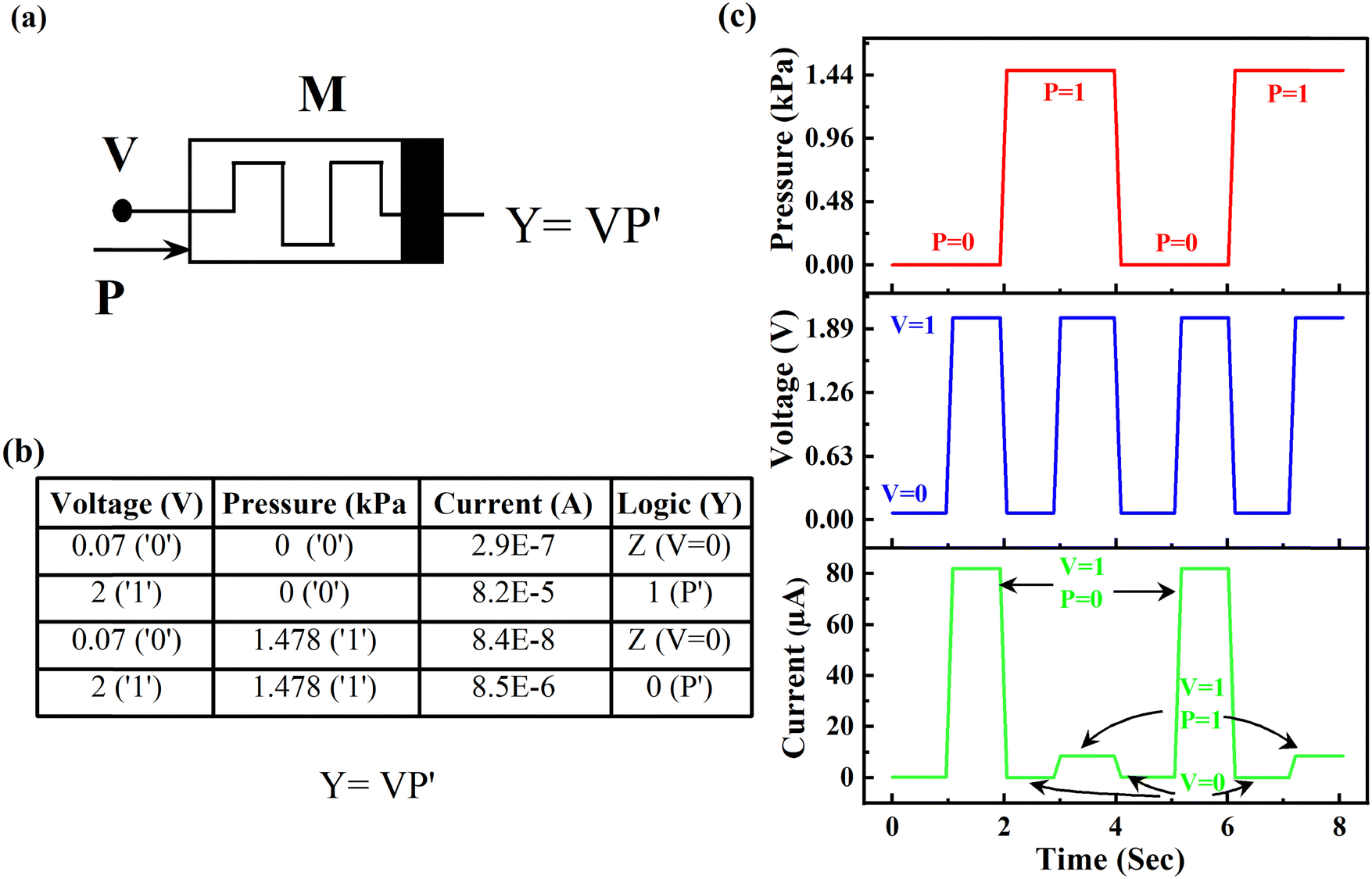 | ||
| Fig. 8 (a) Schematic of memristor with applied pressure (b) truth table of the device derived from the I–V characteristics (c) output current levels as a result of different combinations of applied electrical and pressure logic inputs, read at 2 V with threshold current set to 10 μA. | ||
 | ||
| Fig. 9 (a) Proposed active-low 2:1 MUX logic circuit with the fabricated memristor. (b) The timing diagram of current levels with the pressure of the proposed MUX logic circuit derived from the I–V characteristics (c) Schematic of the proposed active low 2:1 MUX logic (d) truth table of the proposed MUX. | ||
Exploring this unique characteristic, the device's potential is explored for the design of an active low 2:1 multiplexer (MUX) circuit. Two memristors, designated as memristors M0 and M1, with identical features are employed. For better stability of the proposed circuit, pressure (P) is chosen as the input, and voltage (V) is chosen as the ‘enabling signal’, of the 2:1 MUX. Technically, one can choose either the input voltage or the applied pressure as the ‘select input’, and the other as the ‘enabling signal’, and the 2:1 MUX will theoretically work correctly. However, in the practical realization of the circuit, the pressure changes are way more gradual than voltage, and realizing abrupt changes in pressure is challenging. Further, a voltage-enabling signal can be switched very quickly in a MUX. Furthermore, a MUX short-circuits the select input line to the output line based on the choice of the enabling signal. Therefore, the pressure change will still function reliably as the select input, even if it is not as abrupt as the voltage change. Moreover, if the pressure is utilized as the enabling signal, there might be an intermediate stage during its transition where the pressure is neither too high nor too low, leading to a higher region of uncertainty concerning the digital logic at the MUX output. The input of the M0 is named P0, and the input of the M1 is P1, as indicated in Fig. 9(a). The outputs of both memristors are wired-OR connection and labelled as Y. Given the Boolean expression obtained for the fabricated memristor as Y = VP′, the modified inputs for the proposed 2:1 MUX result in the Boolean expression Y = V′P0′ + VP1′. This implies that the voltage will selectively choose either of the inputs of the MUX inputs, with low voltage favouring P0 and vice versa. In the given timing diagram of the applied pressure, applied voltage, the output current of M1, the output current of M0, and the final output Y have been depicted in Fig. 9(b). For a better understanding, the schematic and the truth table of the proposed 2:1 MUX are also shown in Fig. 9(c) and (d). The fabricated bulk SnO2−x memristor exhibits distinct characteristics under SET and RESET voltages with applied pressure.
The key properties of the fabricated Ag/SnO2−x/ITO device, as compared to similar reported studies, are listed in Table 2. This shows Ag/SnO2−x/ITO as a potential low-cost device with appreciable performance with in-memory computing and memlogic abilities. The proposed memlogic applications (as depicted in Fig. 6–9), shown by the memristive device limited to the low-pressure value of ≤1.928 kPa, fall under the range of detectable pressure by human skin (100 Pa to 400 kPa).60 Therefore, the fabricated memristive device-based memlogic operation can potentially find its place and may be limited to soft-robotic applications, such as adaptive robotic skin, where remembrance and in situ real-time logical processing of tactile sensations are important.60–62 Such advanced applications for the next-generation reconfigurable piezoelectric circuits for future AI hardware designs utilizing the fabricated memristive device shall be taken up for future scope of work.
| Properties | Ref. 63 | Ref. 64 | Ref. 65 | Ref. 44 | Ref. 66 | This work | |
|---|---|---|---|---|---|---|---|
| Device structure | ITO/CeO2−x/AlOy/Al | Ti/Pt/NbOx/Ti/Pt | Si/NbOx/Tin | s-ITO/c-ITO | Ag/AgOx/Ag | Ag/SnO2−x/ITO | |
| Memlogic | Yes | No | No | No | Yes | Yes | |
| Fabrication process | Magnetron sputtering | Magnetron sputtering | Magnetron sputtering | Magnetron sputtering | Thermal oxidation | Hydrothe-rmal | |
| I ON/IOFF | 14 | 103 | 33 | ||||
| Cyclic endurance | 30 | 50 | 220 | 100 | 100 | ||
| Resistance window | 105 | 2.29 × 10⁵ | |||||
| External stimuli | Optical | Yes | Yes | ||||
| Mechanical pressure | No | Yes | Yes | Yes | Yes | Yes | |
4. Conclusion
The hydrothermal synthesis of SnO2−x and fabricated Ag/SnO2−x/ITO device demonstrated bipolar resistive switching phenomena. The larger concentration of oxygen vacancy and Schottky barrier enabled the resistive switching phenomena of the device. Based on the pressure dependent current–voltage characteristics in absence and presence of pressure, inverter and active-low 2:1 multiplexer as memlogic applications were proposed. This in-memory computing feature of the device makes it a potential candidate for the next-generation reconfigurable peizoelectronic circuits for future AI hardware designs.
5. Experimental section
5.1. Materials and characterization
A polyethylene terephthalate (PET) sheet with a coated layer of indium tin oxide (ITO) was procured from Sigma-Aldrich, and pure silver (metal pellet) was used as received. The structural and phase identification study of the grown tin oxide layer was done by the XRD method (RIGAKU ULTIMA-IV instrument with Cu-Kα X-ray source). A Thermo Scientific Multilab 2000 with Al Kα radiation operated at 15 kV, XPS instrument was employed to investigate the tin oxide material's oxidation states and chemical composition. The field emission scanning electron microscopy (FESEM) images were obtained by an FEI, LoVac Apreo electron microscope. Keithley 2450 source meter and a DC probe station were utilized for the electrical characterizations of the fabricated devices.5.2. Material synthesis and device fabrication
The schematic of the tin oxide synthesis procedure and Ag/SnO2−x/ITO structured device fabrication is illustrated in Fig. S1, ESI.†
Author contributions
Bishal Kumar Keshari: conceptualization, data curation, formal analysis, investigation, methodology, visualization, writing – original draft. Soumi Saha: data curation, formal analysis, visualization, writing. Sanghamitra DebRoy: methodology, writing – review & editing. Akshay Salimath: methodology, writing – review & editing. Venkat Mattela: methodology, writing – review & editing. Subhradeep Pal: supervision, formal analysis, writing – review & editing. Surya Shankar Dan: supervision, formal analysis, writing – review & editing. Parikshit Sahatiya: supervision, formal analysis, funding, writing – review & editing.Conflicts of interest
There are no conflicts to declare.Data availability
The data supporting the reported study have been included within this article or from the corresponding author upon request.Acknowledgements
The authors are grateful to the Central Analytical Laboratory, Birla Institute of Technology and Science Pilani, Hyderabad Campus, for the provided support in material characterizations.References
- A. R. Patil, T. D. Dongale, R. K. Kamat and K. Y. Rajpure, Binary metal oxide-based resistive switching memory devices: A status review, Mater. Today Commun., 2023, 34, 105356 CrossRef CAS.
- W. Chen, et al., Essential Characteristics of Memristors for Neuromorphic Computing, Adv. Electron. Mater., 2023, 9, 2200833 CrossRef CAS.
- R. Waser and M. Aono, Nanoionics-based resistive switching memories, Nanosci. Technol., 2009, 158–165, DOI:10.1142/9789814287005_0016.
- K. Zhang, Y. Ren, P. Ganesh and Y. Cao, Effect of electrode and oxide properties on the filament kinetics during electroforming in metal-oxide-based memories, npj Comput. Mater., 2022, 8, 1–10 CrossRef.
- A. Wedig, et al., Nanoscale cation motion in TaOx, HfOx and TiOx memristive systems, Nat. Nanotechnol., 2016, 11, 67–74 CrossRef CAS PubMed.
- R. Yang, et al., On-demand nanodevice with electrical and neuromorphic multifunction realized by local ion migration, ACS Nano, 2012, 6, 9515–9521 CrossRef CAS PubMed.
- Y. Pan, et al., Mimicking synaptic plasticity and learning behaviours in solution processed SnO2 memristor, J. Alloys Compd., 2018, 757, 496–503 CrossRef CAS.
- K. Komal, G. Gupta, M. Singh and B. Singh, Improved resistive switching of RGO and SnO2 based resistive memory device for non-volatile memory application, J. Alloys Compd., 2022, 923, 166196 CrossRef CAS.
- C. C. Hsu, P. Y. Chuang and Y. T. Chen, Resistive Switching Characteristic of Low-Temperature Top-Electrode-Free Tin-Oxide Memristor, IEEE Trans. Electron Devices, 2017, 64, 3951–3954 CAS.
- C. Guo, M. Cao and C. Hu, A novel and low-temperature hydrothermal synthesis of SnO2 nanorods, Inorg. Chem. Commun., 2004, 7, 929–931 CrossRef CAS.
- S. Anuchai, et al., Low temperature preparation of oxygen-deficient tin dioxide nanocrystals and a role of oxygen vacancy in photocatalytic activity improvement, J. Colloid Interface Sci., 2018, 512, 105–114 CrossRef CAS PubMed.
- L. Zhang, et al., Facile one-step hydrothermal synthesis of SnO2 microspheres with oxygen vacancies for superior ethanol sensor, J. Alloys Compd., 2020, 814, 152266 CrossRef CAS.
- Y. Li, et al., A robust graphene oxide memristor enabled by organic pyridinium intercalation for artificial biosynapse application, Nano Res., 2023, 36–40, DOI:10.1007/s12274-023-5789-5.
- L. Chua, G. C. Sirakoulis and A. Adamatzky, Handbook of Memristor Networks, 2019 DOI:10.1007/978-3-319-76375-0.
- H. Abderrahim, et al., Measure of carbon dioxide using a gas sensor of a semiconductor type: Based on tin dioxide (sno2), J. Mater. Environ. Sci., 2011, 2, 94–103 CAS.
- Z. Li, W. Zeng and Q. Li, SnO2 as a gas sensor in detection of volatile organic compounds: A review, Sens. Actuators, A, 2022, 346, 113845 CrossRef CAS.
- Y. Kong, et al., SnO2 nanostructured materials used as gas sensors for the detection of hazardous and flammable gases: A review, Nano Mater. Sci., 2022, 4, 339–350 CrossRef CAS.
- J. M. Wu and C. H. Kuo, Ultraviolet photodetectors made from SnO2 nanowires, Thin Solid Films, 2009, 517, 3870–3873 CrossRef CAS.
- P. Chetri and J. C. Dhar, Improved photodetector performance of SnO2 nanowire by optimized air annealing, Semicond. Sci. Technol., 2020, 35, 045014 CrossRef CAS.
- B. Du, K. He, G. Tian, X. Che and L. Song, Robust electron transport layers of SnO2 for efficient perovskite solar cells: recent advances and perspectives, J. Mater. Chem. C, 2023, 11, 13625–13646 RSC.
- X. Wang, et al., Sea urchin-like microstructures pressure sensors with ultra-sensitivity and super working range, ResearchSquare, 2020, 1, 1–23 Search PubMed.
- F. Zhou and Y. Chai, Near-sensor and in-sensor computing, Nat. Electron, 2020, 3, 664–671 CrossRef.
- Z. Lv, et al., Self-assembling crystalline peptide microrod for neuromorphic function implementation, Matter, 2021, 4, 1702–1719 CrossRef CAS.
- Z. Lv, et al., Development of Bio-Voltage Operated Humidity-Sensory Neurons Comprising Self-Assembled Peptide Memristors, Adv. Mater., 2024, 36, 1–13 Search PubMed.
- A. Debataraja, et al., Investigation of Nanostructured SnO2 Synthesized with Polyol Technique for CO Gas Sensor Applications, Procedia Eng., 2017, 170, 60–64 CrossRef CAS.
- Y. Xu, et al., Oxygen Vacancies Enabled Porous SnO2 Thin Films for Highly Sensitive Detection of Triethylamine at Room Temperature, ACS Appl. Mater. Interfaces, 2020, 12, 20704–20713 CrossRef CAS PubMed.
- Q. Liu, et al., High Visible Light Photocatalytic Activity of SnO2-x Nanocrystals with Rich Oxygen Vacancy, Eur. J. Inorg. Chem., 2021, 4370–4376 CrossRef CAS.
- Y. Wei, C. Chen, G. Yuan and S. Gao, SnO2 nanocrystals with abundant oxygen vacancies: Preparation and room temperature NO2 sensing, J. Alloys Compd., 2016, 681, 43–49 CrossRef CAS.
- S. Halder, C. J. Keerthi, C. Chakraborty and S. Pal, Donor-Acceptor Covalent Organic Polymer Framework for High-Performance Broadband Flexible Photodetector, IEEE J. Sel. Top. Quantum Electron., 2023, 1–8 Search PubMed.
- A. Kumar, et al., Forming-free high-endurance Al/ZnO/Al memristor fabricated by dual ion beam sputtering, Appl. Phys. Lett., 2017, 110, 253509 CrossRef.
- R. Waser, R. Dittmann, C. Staikov and K. Szot, Redox-based resistive switching memories nanoionic mechanisms, prospects, and challenges, Adv. Mater., 2009, 21, 2632–2663 CrossRef CAS PubMed.
- W. S. Choi, M. S. Song, H. Kim and D. H. Kim, Conduction Mechanism Analysis of Abrupt- and Gradual-Switching InGaZnO Memristors, Micromachines, 2022, 13, 1–10 Search PubMed.
- J. Yu, et al., Resistive switching properties of polycrystalline HfO x N y films by plasma-enhanced atomic layer deposition, Jpn. J. Appl. Phys., 2017, 56, 050304 CrossRef.
- S. Munjal and N. Khare, Advances in resistive switching based memory devices, J. Phys. D: Appl. Phys., 2019, 52, 433002 CrossRef CAS.
- S. P. Swathi, A. Makkaramkott and A. Subramanian, Tin Oxide Nanorod Array-Based Photonic Memristors with Multilevel Resistance States Driven by Optoelectronic Stimuli, ACS Appl. Mater. Interfaces, 2023, 15, 15676–15690 CrossRef CAS PubMed.
- A. Baranowska-Korczyc, et al., A SnO2shell for high environmental stability of Ag nanowires applied for thermal management, RSC Adv., 2021, 11, 4174–4185 RSC.
- S. Penukula, et al., Barrier layer design reduces top electrode ion migration in perovskite solar cells, EES Sol., 2025, 1, 345–355 RSC.
- D. H. Kwon, et al., Atomic structure of conducting nanofilaments in TiO2 resistive switching memory, Nat. Nanotechnol., 2010, 5, 148–153 CrossRef CAS PubMed.
- G. Di Martino, et al., Real-time in situ optical tracking of oxygen vacancy migration in memristors, Nat. Electron., 2020, 3, 687–693 CrossRef CAS.
- J. J. Yang, D. B. Strukov and D. R. Stewart, Memristive devices for computing, Nat. Nanotechnol., 2013, 8, 13–24 CrossRef CAS PubMed.
- H. S. P. Wong, et al., Metal-oxide RRAM, Proc. IEEE, 2012, 100, 1951–1970 CAS.
- B. Mohammad, et al., State of the art of metal oxide memristor devices, Nanotechnol. Rev., 2016, 5, 311–329 CAS.
- V. Adepu, K. Kamath, V. Mattela and P. Sahatiya, Laser-Assisted Gaussian Microstructure Patterned PDMS Encapsulated Ti3C2Tx(MXene)-Based Pressure Sensor for Object and Touch Detection, IEEE Sens. J., 2021, 21, 16547–16553 CAS.
- X. Han, et al., Highly transparent flexible artificial nociceptor based on forming-free ITO memristor, Appl. Phys. Lett., 2022, 120, 094103 CrossRef CAS.
- M. Yang, et al., High-Performance Flexible Pressure Sensor with a Self-Healing Function for Tactile Feedback, Adv. Sci., 2022, 9, 2200507 CrossRef CAS PubMed.
- A. Huang, et al., A unique, flexible, and porous pressure sensor with enhanced sensitivity and durability by synergy of surface microstructure and supercritical fluid foaming, Appl. Surf. Sci., 2023, 618, 156661 CrossRef CAS.
- O. Glushko, P. Kraker and M. J. Cordill, Explicit relationship between electrical and topological degradation of polymer-supported metal films subjected to mechanical loading, Appl. Phys. Lett., 2017, 110, 1–5 CrossRef.
- X. Chen, et al., Embedding stretchable, mesh-structured piezoresistive sensor for in-situ damage detection of glass fiber-reinforced composite, Compos. Sci. Technol., 2023, 233, 109926 CrossRef CAS.
- S. Das, et al., Controlled manipulation of oxygen vacancies using nanoscale flexoelectricity, Nat. Commun., 2017, 8, 1–8 CrossRef PubMed.
- J. B. Park, et al., Highly sensitive and flexible pressure sensors using position- and dimension-controlled ZnO nanotube arrays grown on graphene films, NPG Asia Mater., 2021, 13, 1–9 CrossRef.
- B. U. Hwang, et al., A transparent stretchable sensor for distinguishable detection of touch and pressure by capacitive and piezoresistive signal transduction, NPG Asia Mater., 2019, 11, 23 CrossRef CAS.
- M. Kölbach, et al., Grain Boundaries Limit the Charge Carrier Transport in Pulsed Laser Deposited α-SnWO4Thin Film Photoabsorbers, ACS Appl. Energy Mater., 2020, 3, 4320–4330 CrossRef.
- D. Juan, M. Pruneda and V. Ferrari, Localized electronic vacancy level and its effect on the properties of doped manganites, Sci. Rep., 2021, 11, 1–11 CrossRef PubMed.
- C. Drouilly, et al., ZnO oxygen vacancies formation and filling followed by in situ photoluminescence and in situ EPR, J. Phys. Chem. C, 2012, 116, 21297–21307 CrossRef CAS.
- Z. Xu, et al., Preparation of organic N-fused perylenediimide-MXene hybrid material for robust versatile memristive device, Int. J. Extrem. Manuf., 2025, 7, 025507 CrossRef CAS.
- S. Ling, S. Lin, Y. Wu and Y. Li, Toward highly-robust MXene hybrid memristor by synergetic ionotronic modification and two-dimensional heterojunction, Chem. Eng. J., 2024, 486, 150100 CrossRef CAS.
- W. Zhang, et al., Synchronous Regulation of Hydrophobic Molecular Architecture and Interface Engineering for Robust WORM-Type Memristor, Adv. Funct. Mater., 2024, 2404625, 1–11 Search PubMed.
- W. Sun, et al., Understanding memristive switching via in situ characterization and device modeling, Nat. Commun., 2019, 10, 1–13 CrossRef PubMed.
- T. Hussain, et al., Cellulose Nanocrystal Based Bio-Memristor as a Green Artificial Synaptic Device for Neuromorphic Computing Applications, Adv. Mater. Technol., 2022, 7, 2100744 CrossRef CAS.
- S. Lee, et al., Beyond Human Touch Perception: An Adaptive Robotic Skin Based on Gallium Microgranules for Pressure Sensory Augmentation, Adv. Mater., 2022, 34, 2204805 CrossRef CAS PubMed.
- P. Wang, et al., Surface engineering via self-assembly on PEDOT: PSS fibers: Biomimetic fluff-like morphology and sensing application, Chem. Eng. J., 2021, 425, 131551 CrossRef CAS.
- Q. Su, et al., A stretchable and strain-unperturbed pressure sensor for motion interference-free tactile monitoring on skins, Sci. Adv., 2021, 7, eabi4563 CrossRef PubMed.
- H. Tan, et al., Light-Gated Memristor with Integrated Logic and Memory Functions, ACS Nano, 2017, 11, 11298–11305 CrossRef CAS PubMed.
- J. Zhu, et al., An Artificial Spiking Nociceptor Integrating Pressure Sensors and Memristors, IEEE Electron Device Lett., 2022, 43, 962–965 CAS.
- X. Zhang, et al., An artificial spiking afferent nerve based on Mott memristors for neurorobotics, Nat. Commun., 2020, 11, 1–9 Search PubMed.
- B. K. Keshari, et al., Light- and Pressure-Stimulated Silver Oxide (AgOx) - Based Memristors for In-Sensor Memory and Computing Applications, ACS Appl. Electron. Mater., 2024, 6, 1007–1017 CrossRef CAS.
Footnote |
| † Electronic supplementary information (ESI) available. See DOI: https://doi.org/10.1039/d5tc01687h |
| This journal is © The Royal Society of Chemistry 2025 |