
 Open Access Article
 This Open Access Article is licensed under a Creative Commons Attribution-Non Commercial 3.0 Unported Licence
Electrically erasable multi-level charge trapping memory with metal nanoparticle engineering for organic synaptic transistors†
Yujeong
Hwang
a,
Yeon-Woo
Lee
b,
Chang-Hyun
Kim
 c,
Hea-Lim
Park
*b and
Min-Hoi
Kim
*a
c,
Hea-Lim
Park
*b and
Min-Hoi
Kim
*a
aDepartment of Creative Convergence Engineering, Hanbat National University, Daejeon 34158, Republic of Korea. E-mail: mhkim8@hanbat.ac.kr
bDepartment of Materials Science and Engineering, Seoul National University of Science and Technology, Seoul 01811, Republic of Korea. E-mail: parkhl21@seoultech.ac.kr
cSchool of Electrical Engineering and Computer Science, University of Ottawa, Ottawa, ON KIN 6N5, Canada
First published on 29th April 2025
Abstract
The development of wearable neuromorphic electronics is critical for advancing human–machine interfaces, personalized healthcare, and brain-inspired computing. Organic synaptic transistors (OSTs) have emerged as promising candidates due to their biocompatibility, mechanical flexibility, and tunable optoelectronic properties by molecular design. However, achieving efficient electrical erasing in charge-trapping-based OSTs remains challenging, particularly for oligomeric semiconductors with relatively large bandgaps. Here, we introduce a novel approach to enhance the vertical electric field in OSTs by incorporating metal nanoparticles (NPs) on top of a wide-bandgap organic semiconductor, significantly improving erase operations. The proposed device demonstrates an enlarged memory window and successful realization of 30 distinct potentiation and depression states, overcoming the write-once-read-many limitation observed in conventional charge-trapping devices. Furthermore, neural network simulations employing our multi-level memory states achieved an 87.3% classification accuracy on hand-written digit dataset, comparable to software-based systems. This work provides a simple yet efficient strategy for engineering neuromorphic transistors, paving the way for next-generation artificial intelligence hardware.
1. Introduction
The growing demand for human–machine interfaces, personalized healthcare, and brain-inspired computing highlights the critical need for wearable neuromorphic platforms that seamlessly integrate with the human body.1–8 These flexible neuromorphic electronics address the fundamental limitations of conventional electronic systems by enabling real-time health monitoring, personalized information processing, and interactive communication, while mimicking the brain's neural processing with ultralow power consumption (Fig. 1a).9–15 Among the various materials used in flexible neuromorphic electronics, organic artificial synapses have garnered significant attention due to their tunable optical and electrical properties through molecular design, scalability, low-cost fabrication, biocompatibility, and mechanical flexibility.16–28 In particular, organic synaptic transistors (OSTs) based on charge-trapping mechanisms have been extensively studied for their advantages, including the ability to achieve multiple memory states by modulating the trapped charge density and their excellent data retention characteristics.29–33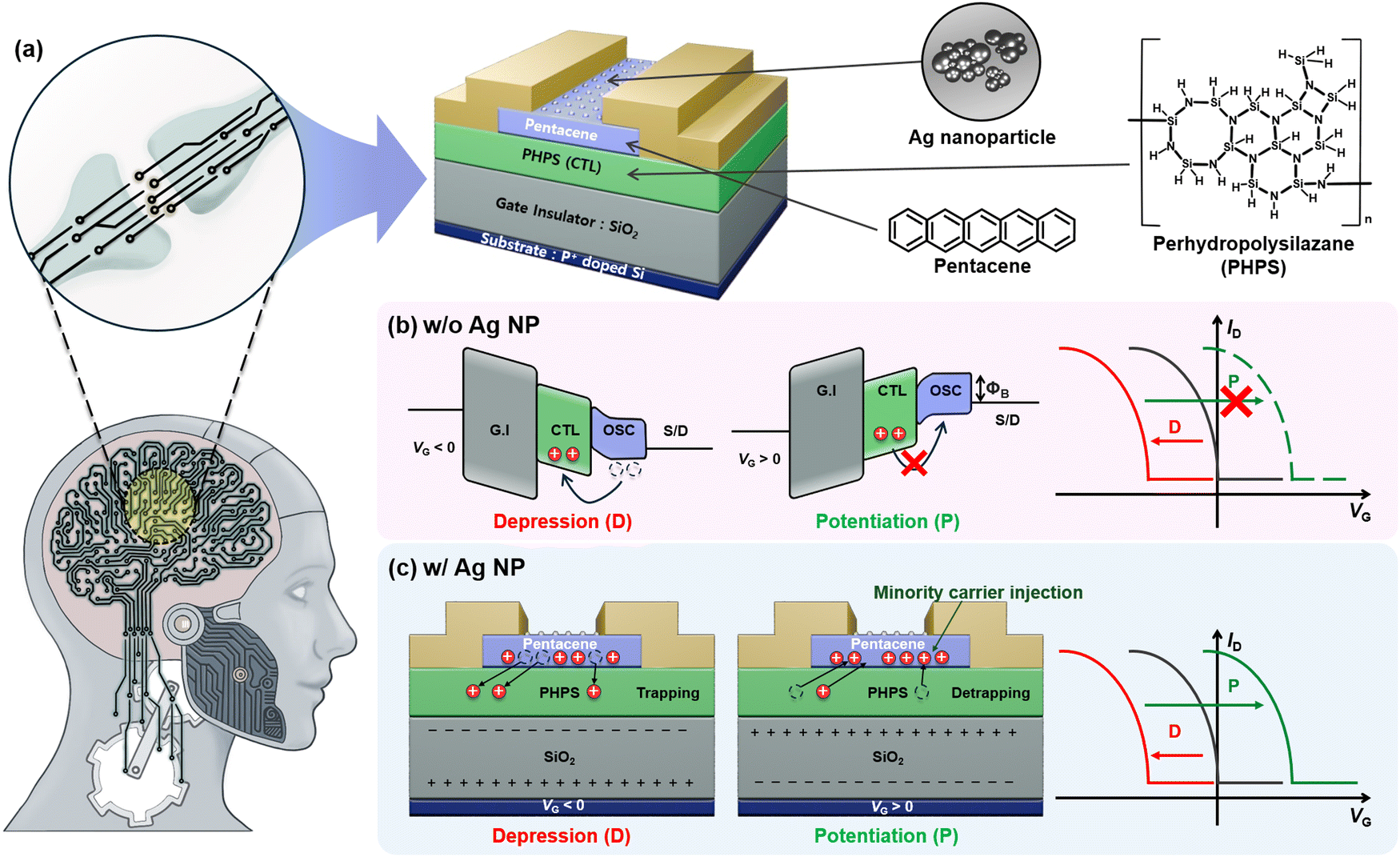 | ||
| Fig. 1 (a) Schematic of charge-trapping-based OSTs with metal NPs for electrically writable (depression; D) and erasable (potentiation; P) multi-memory states in neuromorphic computing. (b) Challenges in electrical erase operations (P) of charge-trapping-based OSTs with oligomeric semiconductors. (c) Realization of electrically writable (D) and erasable (P) multi-memory states by introducing metal NPs on top of the OSC layer. | ||
Among the diverse organic semiconductors employed in charge-trapping-based organic synapses, oligomeric semiconductors offer excellent crystallinity and high uniformity due to their compatibility with vacuum deposition processes, which prevents damage to underlying layers.34–36 However, most oligomeric semiconductors possess a relatively large bandgap of approximately 2.0 eV, which has been reported to hinder electrical erase operations in charge-trapping devices.37–39 During the erase process, the channel region remains in a depleted state due to the high minority charge injection barrier, resulting in only a negligible vertical electric field from the semiconductor to the gate, ultimately preventing effective electrical erase operations (Fig. 1(b)). This phenomenon is also observed in large-bandgap inorganic semiconductors such as GaN, SiC, and emerging metal-oxide semiconductors like In–Ga–Zn oxide. To overcome this limitation, strategies such as incorporating high-work-function materials as source/drain (S/D) electrodes and scaling down the channel length to 20 nm to enhance the vertical electric field strength have been proposed in inorganic memory devices, enabling erase performance.39 As a solution to this challenge in artificial synaptic devices, optical erasing operations have been widely explored.38–40 However, these approaches introduce complex driving schemes that rely on a combination of electrical writing and optical erasing, device instability, or costly and intricate fabrication processes. These limitations hinder the practical implementation of neuromorphic electronics in real-world applications.
In this work, we propose a novel strategy for organic synaptic transistors that addresses this long-standing challenge without relying on optical assistance or complex fabrication techniques. Specifically, we introduce a vertical field-engineering strategy by incorporating metal nanoparticles (NPs) on top of a wide-bandgap oligomeric semiconductor (Fig. 1). The embedded NPs locally enhance the vertical electric field across the channel during erase operations, enabling fully electrical control of both potentiation and depression in charge-trapping-based OSTs—a capability rarely demonstrated in previous oligomer-based synaptic devices. Without this enhancement, the depleted channel region resulted in only a negligible electric field applied to charge trap layer (CTL), preventing effective electrical erase operations. Importantly, this strategy provides a generalizable and scalable solution to achieving fully electrical weight modulation in a broad range of organic semiconductors with large bandgaps.
As a result, the proposed NP-embedded OST exhibits a significantly enlarged memory window of up to 64 V (depending on NP thickness) and demonstrates 30 distinct, electrically controlled potentiation and depression states. In contrast, reference devices without NPs operated only in a write-once-read-many (WORM) mode, lacking electrical erasability. The multi-level conductance states of our device were successfully utilized as synaptic weights in a neural network for handwritten digit classification using the MNIST dataset, achieving a recognition accuracy of 87.3%, approaching the performance of an ideal software-based system.
2. Methods
For both the devices with and without Ag NPs, p-type doped silicon substrates were oxidized to form a 200 nm thick SiO2 layer, which served as the gate insulator. To fabricate the CTL, an 18 wt% solution of perhydropolysilazane (PHPS) was diluted in dibutyl ether, and a 2 wt% PHPS solution was used. The solution was spin-coated at 500 rpm for 5 s, followed by 3000 rpm for 40 s, and subsequently annealed at 100 °C for 2 h.40,41 The oligomeric semiconductor (OSC), pentacene, was thermally vacuum-deposited at a rate of 0.5 Å s−1 to form a 50 nm thick semiconductor layer. Next, Au was thermally vacuum-deposited at a rate of 1 Å s−1 to create a 50 nm thick source/drain (S/D) electrode. The channel length and width of the devices were 200 μm and 1 mm, respectively. For the OSTs incorporating Ag NPs, Ag NPs with thicknesses ranging from 2 nm to 15 nm were deposited via thermal vacuum deposition at a rate of 1 Å s−1 to induce a sufficiently strong electric field throughout the entire CTL (Fig. 1d). The electrical characteristics of the devices were measured under ambient conditions using an HP4155A and 4200A-SCS semiconductor parameter analyzer. A scanning electron microscope (SU8230, AMETEK) was used to analyze the surface morphology of the thermally deposited Ag NPs. Additionally, two-dimensional (2D) finite-element numerical simulation was performed using a commercially available software package (ATLAS, Silvaco). This simulator self-consistently solves the drift-diffusion and Poisson's equations in a user-defined 2D mesh that is designed to mimic the cross-section of the actual device. In this study, we used this method to specifically quantify the electric potential distribution in the channel and the CTL regions, which is known to strongly affect the gate programming and erasing efficiency of the memory transistors.3. Results and discussion
Firstly, scanning electron microscope (SEM) was used to observe surface of the pentacene and the formation of Ag NPs on top of pentacene, an OSC. Fig. S1a and b (ESI†) show the SEM images of the surface morphology of pentacene and 5-nm-thick Ag NPs deposited on pentacene, respectively. Fig. S1a (ESI†) displays typical pentacene grains without the formation of Ag NPs, while Fig. S1b (ESI†) shows the surface of smaller Ag NP grains deposited on pentacene, with a grain size similar to that of the pentacene in Fig. S1a (ESI†).42 From this, we confirmed the successful formation of Ag NPs on the pentacene layer through the thermal evaporation of 5-nm thick Ag.To investigate the effect of Ag NPs on the electric field distribution in OSTs, we conducted numerical simulations of the electrical potential distribution (Fig. 2 and Fig. S2, ESI†). The simulation results, shown in Fig. 2a–d, illustrate the potential distribution without and with Ag NPs during the write (Fig. 2a and b) and erase operations (Fig. 2c and d). The simulations were performed on a portion of the source electrode and in a 200-nm-wide region near the source electrodes (green dotted box in Fig. S2, ESI†). Specifically, for the device with Ag NPs, the simulation assumed that both the size and spacing of the metal nanoparticles were on the order of 10 nm. In our device structure, where a 5-nm-thick Ag nanoparticle layer was deposited on a relatively thick (50-nm) pentacene OSC layer, the influence of Ag diffusion is expected to be negligible. Therefore, the effect of Ag diffusion was not considered in our numerical simulations. In both cases, with and without Ag NPs, the region where the S/D and gate electrode overlap is designated as region A (red dotted line in Fig. 2 and Fig. S2, ESI†), while the region where the gate electrode overlaps the channel without overlapping the S/D is referred to as region B (orange dotted line in Fig. 2 and Fig. S2, ESI†). Fig. 2a and b show the electric potential distribution of OSTs without and with Ag NPs, respectively, during the write operation at a gate voltage of −90 V. Under this condition (VG = −90 V), holes accumulate readily at the OSC/insulator interface in both devices, increasing the conductivity of the OSC layer. Consequently, the potential distributions in regions A and B remain similar, ensuring the application of a sufficient vertical electric field to the CTL, which facilitates hole trapping. It should be noted that the PHPS CTL possesses a high density of both electron and hole trap sites, allowing the capture of charge carriers depending on the applied electric field. Under a negative gate bias, holes accumulate at the OSC/PHPS interface and are subsequently trapped at the hole trap sites within the PHPS CTL, resulting in nonvolatile memory behavior.38,40 Accordingly, successful write operations are observed in both OST devices, as evidenced by the negative shift in the transfer curves (red lines with circles in Fig. 2e and f). During the erase operation under a positive gate voltage (VG,Bias = +90 V), electrons encounter a high injection barrier from the S/D electrode to the OSC layer, leaving the OSC layer in a depletion state. Region A where the thickness between the source and gate electrodes is on the order of several hundred nanometers, exhibits a vertical potential gradient under conditions of the OSC depletion (Fig. 2c and Fig. S2, ESI†). In contrast, in region B, the vertical potential gradient diminishes as the distance from the source increases, implying that the CTL experiences an insufficient electric field. As a result, hole detrapping does not occur in region B, rendering the erase operation ineffective. Fig. S2 (ESI†) presents the simulated result of the entire device without Ag NPs under an erasing voltage (VG,Bias = +90 V), clearly showing the negligible potential gradient throughout region B. This corresponds to the transfer curve of the device without Ag NPs, which remains unchanged even at VG = +90 V (green line with circles in Fig. 2e). In contrast, the OST device with Ag NPs exhibits a vertical potential gradient across both regions A and B during the erase operation, unlike the device without Ag NPs (Fig. 2d). Due to the nanoscale gaps between the source electrode and the NPs, as well as between adjacent NPs, and the conductive nature of Ag NPs, the potential gradient across these nanoscale gaps in lateral direction is negligible. Consequently, these NPs could effectively form an nearly identical potential to that of the source electrode. As a result, a significant potential difference is established in the vertical direction from the OSC to gate electrode, even in region B, where there is no direct overlap with the source electrode. This leads to the generation of a strong bottom-up electric field during the erase operation at positive VG, thereby enabling successful hole detrapping and erasing of the device with 5-nm thick Ag NPs, as shown in the green line with circles in Fig. 2f. Fig. S3 (ESI†) presents the transfer curves of devices incorporating 2-nm and 10-nm thick Ag NPs after the writing and erasing processes. Both devices successfully exhibit writing and erasing characteristics, as indicated by the red and green lines in Fig. S3 (ESI†), respectively.
 | ||
| Fig. 2 Simulated potential distribution results without and with Ag NPs during the (a) and (b) write (depression) and (c), (d) erase (potentiation) operations. Transfer curves of the devices (e) without and (f) with Ag NPs after writing (red line) and erasing (green line), with the black lines representing the initial transfer curves. | ||
Fig. 3a presents a graph of the memory on-current and memory off-current as a function of Ag NP thickness. The values were extracted from Fig. 2e, f, and Fig. S3 (ESI†). For the device without Ag NPs (corresponding to a 0-nm Ag NP thickness), the drain current at a gate voltage of −15 V was defined as the memory on-current and memory off-current. For devices from 2-nm to 15-nm thick Ag NPs, the drain current at a gate voltage of 0 V was used. As the NP thickness increases from the Ag-free device, off-currents remains relatively constant, while the on-current exhibits an increasing trend from 1.57 × 10⁻¹⁰ A to 2.30 × 10⁻⁶ A. However, when the Ag NP thickness reaches 15 nm or more, the source and drain become shorted, causing the compliance current (10 mA) to flow. This phenomenon would be attributed to the complete coverage of Ag NPs over the pentacene surface, leading to direct connection between the source and drain electrodes. Fig. 3b shows the memory window of the OSTs as a function of Ag NP thickness. Here, the threshold voltage was defined as the gate voltage at which the drain current reaches 1 nA in each transfer curve, while the memory window was determined by the difference in threshold voltage between the write and erase operations.43–45 For the device without Ag NPs (0-nm Ag NPs), the memory window is negligible. However, for devices with Ag NP thicknesses ranging from 2 nm to 10 nm, the memory window significantly increased from 43 V to 64 V, exceeding 50 V as the NP thickness increased. The mobility values remained relatively constant at approximately 0.07 cm2 V−1 s−1 for devices with Ag NP thicknesses ranging from 0 nm to 5 nm (Fig. 3c). In contrast, a significant increase in mobility to 0.22 cm2 V−1 s−1 was observed for the device with a 10-nm-thick Ag NP layer. This enhancement is presumably due to the extensive coverage of Ag NPs on the pentacene layer, as evidenced in Fig. S4 (ESI†), which likely improves the effective conductivity of the channel. In addition, the devices without Ag NPs and those with 2-nm, 5-nm, and 10-nm thick Ag NPs exhibit similar values of 2.20, 2.57, 2.41, and 1.70 V dec−1, respectively, within the margin of error (Fig. 3d). Fig. 3e presents the reliable memory characteristics observed over 10 cycles of writing and erasing processes. This evaluation involved analyzing the threshold voltage shift in two types of OSTs—one without Ag NPs and one with Ag NPs. The threshold voltage was defined as in Fig. 3a.43 As demonstrated in Fig. 2, the device without Ag NPs failed to perform the erase operation after the write operation, resulting in nearly similar threshold voltages for both states. In contrast, in Ag NP-deposited devices, the threshold voltage shifts repeatedly in the negative direction after the write operation and in the positive direction after the erase operation, unlike in the Ag-free device. Fig. 3f and g illustrate the retention characteristics of OSTs without and with Ag NPs. As shown in Fig. 3f, the erase operation does not occur in the Ag-free device, leading to negligible differences between the on-current and off-current. However, in the OST with 5-nm thick Ag NPs, the on-current (4.81 × 10⁻⁷ A) and off-current (9.38 × 10⁻¹² A) were maintained for up to 1000 s. Similarly, OSTs with 2-nm and 10-nm thick Ag NPs exhibited good retention characteristics, comparable to the 5-nm thick device (Fig. S5, ESI†). To explore the applicability of other metal materials, Au and Al—both widely used in organic electronics—were employed as S/D electrodes in the proposed OSTs with metal NPs. Fig. S6 (ESI†) presents the electrical characteristics of NP-based OSTs with three different metal electrodes (Au, Ag, and Al) as a function of deposition thickness. In the case of Au NPs, the device exhibited both writing and erasing operations, similar to Ag NP-based devices. However, it showed relatively higher off-current levels even at a metal thickness of 2 nm (Fig. S6a, ESI†). This can be attributed to the low energy barrier between the Au NPs and the pentacene layer, which facilitates charge movement and results in a high off-current. At a thickness of 5 nm, the off-current further increased, leading to a low on/off current ratio of approximately one order of magnitude (Fig. S6b, ESI†). When the Au NP thickness reached 15 nm, the device ceased to function normally, as the source and drain electrodes became shorted, causing the current to reach the compliance level (Fig. S6c, ESI†). For comparison, the electrical characteristics of Ag NP-based devices are shown alongside Au and Al NP-based devices in Fig. S6d–f (ESI†). Regarding Al NPs, aluminum is easily oxidized, which inhibits charge transport. At thicknesses of 1 nm and 5 nm, the deposited Al failed to function as a conductive region capable of enhancing the vertical electric field during the erasing operation, unlike Au and Ag NPs. As a result, devices with 2-nm and 5-nm thick Al NPs did not exhibit erasing functionality (Fig. S6g and h, ESI†). Additionally, due to Al's tendency to form a continuous thin film, the Al NP-based device with a thickness of 7 nm became shorted between the source and drain electrodes, leading to a compliance current level (Fig. S6i, ESI†). From these results, we could conclude that Ag NPs, compared to Au and Al, provide an optimal energy barrier with the pentacene layer, while also benefiting from a higher work function than Al, which prevents oxidation. As a result, devices incorporating Ag NPs with thicknesses ranging from 2 nm to 10 nm demonstrated reliable writing and erasing operations along with good electrical performance. The sufficient process margin of Ag deposition thickness ensures the fabrication of reliable and stable synaptic transistors for next-generation computing components. Thus, Ag is an appropriate metal material for forming NPs in our proposed device.
 | ||
| Fig. 3 (a) Graph of the memory on-current and memory off-current, (b) memory window, (c) mobility values, and (d) subthreshold voltage values of the OSTs as a function of Ag NP thickness. (e) Ten cycles of writing and erasing processes. Retention characteristics of OSTs (f) without and (g) with Ag NPs. | ||
To verify the applicability of Ag NP-based OSTs for neuromorphic computing, we first controlled the conductance of both devices (without and with Ag NPs) using gate voltage spikes, as shown in Fig. 4a and b. The multi-conductance levels, representing the memory states of the OSTs, demonstrate the devices' ability to reliably mimic the synaptic weights of biological synapses. In the reference device (Fig. 4a), depression characteristics were achieved at VG = −20 V for 0.5 s at the read voltage of VD = −5 V. Potentiation was induced using electrical spikes of VG = 39 V at the read voltage of VD = −5 V. However, during the potentiation process (erasing operation), the device failed to exhibit erasing behavior or synaptic potentiation characteristics due to an insufficient vertical electric field, instead maintaining constant conductance memory levels throughout the erasing process. In contrast, our proposed synaptic device incorporating Ag NPs exhibited 30 distinct levels of depression and potentiation. Furthermore, as shown in Fig. 4c, it demonstrated reliable operation of five cycles of 30-state potentiation and depression. Specifically, 30 depression levels were achieved at VG = −20 V for at the read voltage of VD = −5 V, while 30 potentiation levels were induced by electrical spikes of VG = 30 V at the read voltage of VD = −5 V. Note that the symmetry between potentiation and depression characteristics could be further enhanced by optimizing the erasing process, such as through tuning the erase pulse waveform and amplitude.46 As previously explained, the presence of Ag NPs enhanced the vertical electric field strength in our device, enabling both the erasing process and synaptic potentiation (observed as a significant positive shift in the transfer curve away from its initial state). This resulted in an enlarged memory window, an increased on/off ratio, and stable potentiation/depression characteristics. By introducing Ag NPs to modulate the vertical electric field, we successfully demonstrated a 30-state multi-memory level and stable synaptic potentiation/depression properties, which could not be achieved in the reference OST. Our device exhibited superior performance metrics, including memory window, the number of distinct conductance states for potentiation and depression, conductance modulation ratio, and energy consumption, compared to previously reported oligomeric synaptic transistors demonstrating potentiation and depression characteristics solely controlled by electrical pulses (Table S1, ESI†).
 | ||
| Fig. 4 (a) Multi-level conductance of both devices without and (b) with Ag NPs using gate voltage spikes. (c) Five cycles of 30-state potentiation and depression in the proposed device with Ag NPs. (d) Hardware neural network consisting of three layers (784 input neurons, 32 processing neurons, and 10 output neurons corresponding to digit classes) for recognizing handwritten digit. (e) OST cell arrays individually serving as artificial synapses connecting the neuron layers for hardware neural network. (f) Channel conductance-level distribution between the first and second neuron layers and (g) between the second and third layers after 100 training epochs. (h) Classification accuracy of the hardware neural network employing our OSTs, achieving 87.3% in classifying handwritten digits. | ||
To evaluate the potential of our proposed OSTs for computing applications, hardware-based neural networks were implemented using our device cells as artificial synapses. Numerical simulations were conducted to assess system performance in handwritten digit recognition tasks using the MNIST dataset. As illustrated in Fig. 4d, the neural network architecture comprised three layers: 784 input neurons, 32 hidden neurons, and 10 output neurons corresponding to digit classes. Our OST cells served as artificial synapses connecting the neuron layers (Fig. 4e). A non-negative weight was employed to efficiently map the weight value onto the conductance of the hardware synapse cell. To emulate real hardware behavior, ideal weights were calculated from software-based training for 100 epochs with 60![[thin space (1/6-em)]](https://www.rsc.org/images/entities/char_2009.gif) 000 MNIST images. At the software training level, the softmax activation function was applied for the output value.47 The training process utilized the adaptive momentum estimation optimizer48 and the sparse categorical cross-entropy loss function.49 The weights were quantized into 30 discrete levels, corresponding to the available conductance states of the synaptic devices. Fig. 4f and g show the resulting conductance distributions after training, corresponding to synaptic connections between the first and second neuron layers, and between the second and third layers, respectively. For performance evaluation, the system's ability to classify 10000 test images from the MNIST dataset was examined. Notably, the hardware neural network employing our OSTs achieved a classification accuracy of 87.3%, approaching the ideal software-based accuracy of ∼93.0% (Fig. 4h). This accuracy could likely be attributed to the gradual and linear potentiation characteristics of our devices.
000 MNIST images. At the software training level, the softmax activation function was applied for the output value.47 The training process utilized the adaptive momentum estimation optimizer48 and the sparse categorical cross-entropy loss function.49 The weights were quantized into 30 discrete levels, corresponding to the available conductance states of the synaptic devices. Fig. 4f and g show the resulting conductance distributions after training, corresponding to synaptic connections between the first and second neuron layers, and between the second and third layers, respectively. For performance evaluation, the system's ability to classify 10000 test images from the MNIST dataset was examined. Notably, the hardware neural network employing our OSTs achieved a classification accuracy of 87.3%, approaching the ideal software-based accuracy of ∼93.0% (Fig. 4h). This accuracy could likely be attributed to the gradual and linear potentiation characteristics of our devices.
These results highlight the potential of the developed OSTs as promising synaptic elements for hardware-based neural networks, capable of supporting advanced computing applications such as pattern recognition, image processing, and motion detection. Furthermore, the demonstrated multi-level conductance modulation and enlarged on/off current ratio provide valuable design insights for overcoming the intrinsic limitations of conventional charge-trapping devices, particularly their write-once-read-many (WORM) behavior in the absence of Ag nanoparticles.
4. Conclusions
In summary, we have demonstrated a novel approach to overcoming the longstanding challenge of electrical erase operations in charge-trapping-based OSTs by integrating metal NPs atop a wide-bandgap oligomeric semiconductor. The inclusion of Ag NPs effectively modulated the vertical electric field, enabling both electrical writing and erasing, which was previously unattainable in conventional devices. Our proposed strategy significantly expanded the memory window, achieving 30 distinct potentiation and depression states with stable retention and endurance characteristics. Furthermore, numerical simulations and experimental analyses confirmed that the enhanced vertical electric field facilitated efficient hole detrapping during the erase process, thereby enabling reliable bidirectional modulation of synaptic weights. This advancement was successfully applied to a neuromorphic computing system, where our Ag NP-based OSTs achieved an MNIST classification accuracy of 87.3%, comparable to ideal software-based implementations. The findings of this study provide a promising pathway for the development of next-generation flexible neuromorphic electronics. By addressing a key limitation in organic artificial synapses, our approach paves the way for the practical implementation of wearable and further bio-integrated neuromorphic systems, advancing the frontier of human–machine interfacing, personalized healthcare, and brain-inspired computing.Author contributions
Y. H., Y.-W. L., H.-L. P., and M.-H. K. initiated and designed the experiments, analyzed the data, and wrote the draft of the manuscript. Y. H. and Y.-W. L. fabricated and characterized the devices. Y. H. measured the electrical characteristics of the devices. C.-H. K. performed and analyzed numerical simulations. All authors discussed the results and commented on the manuscript.Data availability
The data supporting this article have been included as part of the ESI.†Conflicts of interest
The authors declare no competing financial interest.Acknowledgements
This research was supported by Basic Science Research Program through the National Research Foundation of Korea (NRF) funded by the Ministry of Education (2018R1A6A1A03026005) and was supported by the research fund of Hanbat National University in 2024.References
- H. L. Park, M. H. Kim, H. Kim and S. H. Lee, Self-Selective Organic Memristor by Engineered Conductive Nanofilament Diffusion for Realization of Practical Neuromorphic System, Adv. Electron. Mater., 2021, 7, 2100299, DOI:10.1002/aelm.202100299.
- M. W. Park, D. Y. Kim, U. An, J. Jang, J. H. Bae, I. M. Kang and S. H. Lee, Organizing Reliable Polymer Electrode Lines in Flexible Neural Networks via Coffee Ring-Free Micromolding in Capillaries, ACS Appl. Mater. Interfaces, 2022, 14, 46819, DOI:10.1021/acsami.2c13780.
- U. Jung, M. Kim, J. Jang, J. H. Bae, I. M. Kang and S. H. Lee, Formation of Cluster-Structured Metallic Filaments in Organic Memristors for Wearable Neuromorphic Systems with Bio-Mimetic Synaptic Weight Distributions, Adv. Sci., 2024, 11, 2307494, DOI:10.1002/advs.202307494.
- H. Kim, M. Kim, A. Lee, H. L. Park, J. Jang, J. H. Bae, I. M. Kang, E. S. Kim and S. H. Lee, Organic Memristor-Based Flexible Neural Networks with Bio-Realistic Synaptic Plasticity for Complex Combinatorial Optimization, Adv. Sci., 2023, 10, 2300659, DOI:10.1002/advs.202300659.
- S. Oh, H. Kim, S. E. Kim, M. H. Kim, H. L. Park and S. H. Lee, Biodegradable and Flexible Polymer-Based Memristor Possessing Optimized Synaptic Plasticity for Eco-Friendly Wearable Neural Networks with High Energy Efficiency, Adv. Intell. Syst., 2023, 5, 2200272, DOI:10.1002/aisy.202200272.
- U. Jung, C. J. Beak, K. Kim, J. H. Na and S. H. Lee, Scalable Photo-Responsive Physical Unclonable Functions via Particle Kinetics, ACS Nano, 2024, 18, 27642, DOI:10.1021/acsnano.4c09080.
- J. H. Choi, H. S. Hwang, H. B. Jang, S. U. Kim and H. L. Park, Flexible Phototransistors Integrated with Chiral Liquid Crystal Encapsulating Film for Improving Color Selectivity and Stability, ACS Appl. Electron. Mater., 2024, 6, 8094, DOI:10.1021/acsaelm.4c01439.
- C. J. Beak, J. Lee, J. Kim, J. Park and S. H. Lee, Filamentary-Based Organic Memristors for Wearable Neuromorphic Computing Systems, Neuromorph. Comput. Eng., 2024, 4, 022001, DOI:10.1088/2634-4386/ad409a.
- K. N. Kim, M. J. Sung, H. L. Park and T. W. Lee, Organic Synaptic Transistors for Bio-Hybrid Neuromorphic Electronics, Adv. Electron. Mater., 2022, 8, 2100935, DOI:10.1002/aelm.202100935.
- S. E. Kim, M.-H. Kim, J. Jang, H. Kim, S. Kim, J. Jang, J.-H. Bae, I. M. Kang and S.-H. Lee, Systematic Engineering of Metal Ion Injection in Memristors for Complex Neuromorphic Computing with High Energy Efficiency, Adv. Intell. Syst., 2022, 4, 2200110, DOI:10.1002/aisy.202200110.
- H. Kim, J. Lee, H. W. Kim, J. Woo, M. H. Kim and S. H. Lee, Definition of a Localized Conducting Path via Suppressed Charge Injection in Oxide Memristors for Stable Practical Hardware Neural Networks, ACS Appl. Mater. Interfaces, 2023, 15, 51444–51452, DOI:10.1021/acsami.3c13514.
- N. Kim, G. T. Go, H. L. Park, Y. Ahn, J. Kim, Y. Lee, D. G. Seo, W. Lee, Y. H. Kim, H. Yang and T. W. Lee, Molecular Tailoring to Achieve Long-Term Plasticity in Organic Synaptic Transistors for Neuromorphic Computing, Adv. Intell. Syst., 2023, 5, 2300016, DOI:10.1002/aisy.202300016.
- J. S. Ro, H. M. An and H. L. Park, Electrolyte-Gated Synaptic Transistors for Brain-Inspired Computing, Jpn. J. Appl. Phys., 2023, 62, SE0801, DOI:10.35848/1347-4065/acaca4.
- H. M. An, H. Jang, H. Kim, S. D. Lee, S. H. Lee and H. L. Park, Engineered Current Path of Vertical Organic Phototransistors for Smart Optoelectronic Applications, J. Mater. Chem. C, 2023, 11(42), 14580, 10.1039/d3tc02571c.
- H. H. Lee, J. S. Ro, K. N. Kim, H. L. Park and T. W. Lee, Exploring Photosensitive Nanomaterials and Optoelectronic Synapses for Neuromorphic Artificial Vision, Curr. Opin. Solid State Mat. Sci., 2025, 35, 101215, DOI:10.1016/j.cossms.2025.101215.
- H. L. Park, J. Jun, M. H. Kim and S. H. Lee, Introduction of Helical Photonic Crystal Insulator in Organic Phototransistor for Enhancing Selective Color Absorption, Org. Electron., 2022, 100, 106385, DOI:10.1016/j.orgel.2021.106385.
- S. H. Lee, H. L. Park, S. H. Lee, E. K. Noh, S. Hwa, J. Lee, J. H. Lee and M. H. Kim, Systematic Investigation of Subtractive Contact Patterning for High-Resolution Organic Electronic Devices, ACS Appl. Electron Mater., 2023, 5, 2197–2202, DOI:10.1021/acsaelm.3c00080.
- M. J. Kim, C. Lee, E. J. Shin, T. I. Lee, S. Kim, J. Jeong, J. Choi, W. S. Hwang, S. G. Im and B. J. Cho, Highly Reliable Charge Trap-Type Organic Non-Volatile Memory Device Using Advanced Band-Engineered Organic-Inorganic Hybrid Dielectric Stacks, Adv. Funct. Mater., 2021, 31, 2103291, DOI:10.1002/adfm.202103291.
- S. J. Kim and J. S. Lee, Flexible Organic Transistor Memory Devices, Nano Lett., 2010, 10, 2884–2890, DOI:10.1021/nl1009662.
- L. X. Zhang, X. Gao, J. J. Lv, Y. N. Zhong, C. Xu, J. L. Xu and S. D. Wang, Filter-Free Selective Light Monitoring by Organic Field-Effect Transistor Memories with a Tunable Blend Charge-Trapping Layer, ACS Appl. Mater. Interfaces, 2019, 11, 40366–40371, DOI:10.1021/acsami.9b15342.
- H. Dong, X. Fu, J. Liu, Z. Wang and W. Hu, 25th Anniversary Article: Key Points for High-Mobility Organic Field-Effect Transistors, Adv. Mater., 2013, 25(44), 6158–6183, DOI:10.1002/adma.201302514.
- T. Ahn, H. Jung, H. J. Suk and M. H. Yi, Effect of Postfabrication Thermal Annealing on the Electrical Performance of Pentacene Organic Thin-Film Transistors, Synth. Met., 2009, 159, 1277–1280, DOI:10.1016/j.synthmet.2009.02.023.
- C. M. Tran, H. Sakai, Y. Kawashima, K. Ohkubo, S. Fukuzumi and H. Murata, Multi-Level Non-Volatile Organic Transistor-Based Memory Using Lithium-Ion-Encapsulated Fullerene as a Charge Trapping Layer, Org. Electron., 2017, 45, 234–239, DOI:10.1016/j.orgel.2017.03.018.
- S. A. Lee, D. Y. Kim, K. U. Jeong, S. H. Lee, S. Bae, D. S. Lee, G. Wang and T. W. Kim, Molecular-Scale Charge Trap Medium for Organic Non-Volatile Memory Transistors, Org. Electron., 2015, 27, 18–23, DOI:10.1016/j.orgel.2015.08.020.
- K. J. Sarkar, B. Pal and P. Banerji, Graphene Oxide as a Dielectric and Charge Trap Element in Pentacene-Based Organic Thin-Film Transistors for Nonvolatile Memory, ACS Omega, 2019, 4, 4312–4319, DOI:10.1021/acsomega.8b03301.
- L. Han, D. Wang, M. Li, Y. Zhong, K. Liao, Y. Shi and W. Jie, Synaptic Memristors Based on Flexible Organic Pentacene Thin Films by the Thermal Evaporation Method for Neuromorphic Computing, Carbon, 2024, 218, 118665, DOI:10.1016/j.carbon.2023.118665.
- J. Kim, J. Ahn, M. Son, Y. Kim, J. J. Lee, D. Kim, M. C. Chen, S. W. Choi, C. Kim and S. Seo, Solution-Processable Liquid Crystalline Organic Semiconductors Based on 6-(Thiophen-2-Yl)Benzo[b]Thiophene for Organic Thin-Film Transistors, Org. Electron., 2024, 124, 106956, DOI:10.1016/j.orgel.2023.106956.
- Q. D. Ling, D. J. Liaw, C. Zhu, D. S. H. Chan, E. T. Kang and K. G. Neoh, Polymer Electronic Memories: Materials, Devices and Mechanisms, Prog. Polym. Sci., 2008, 33, 917–978, DOI:10.1016/j.progpolymsci.2008.08.001.
- H. S. Lee, J. S. Ro, G. M. Ko and H. L. Park, Flexible and Stretchable Synaptic Devices for Wearable Neuromorphic Electronics, Flex. Print. Electron., 2023, 8, 043001, DOI:10.1088/2058-8585/ad0a37.
- U. C. Jeong, J. S. Ro, H. L. Park and T. W. Lee, Modulating Short-Term and Long-Term Plasticity of Polymer-Based Artificial Synapses for Neuromorphic Computing and Beyond, Neuromorph. Comput. Eng., 2024, 4, 032001, DOI:10.1088/2634-4386/ad5eb5.
- H. Jang, J. Lee, C. J. Beak, S. Biswas, S. H. Lee and H. Kim, Flexible Neuromorphic Electronics for Wearable Near-Sensor and In-Sensor Computing Systems, Adv. Mater., 2025, 37, 2416073, DOI:10.1002/adma.202416073.
- Y. Zhao, S. Lee, T. Long, H. L. Park and T. W. Lee, Natural Biomaterials for Sustainable Flexible Neuromorphic Devices, Biomaterials, 2025, 314, 122861, DOI:10.1016/j.biomaterials.2024.122861.
- J.-H. Choi, H.-M. An and H.-L. Park, Polarized Light-Sensitive Optoelectronic Synapses for Expanding Artificial Vision Systems, Flex. Print. Electron., 2025, 10(1), 013501, DOI:10.1088/2058-8585/adb595.
- J. C. Li, S. S. Wang, X. H. Jian, N. Han and D. C. Ba, Electrical Switching Characteristics of Organic Thin Films Made from Branch Chain Substituted Oligomer as Measured by GaIn Probe, Thin Solid Films, 2011, 520, 712–716, DOI:10.1016/j.tsf.2011.06.093.
- W. Lin, G. Chen, E. Li, L. He, W. Yu, G. Peng, H. Chen and T. Guo, Nonvolatile Multilevel Photomemory Based on Lead-Free Double Perovskite Cs2AgBiBr6Nanocrystals Wrapped within SiO2as a Charge Trapping Layer, ACS Appl. Mater. Interfaces, 2020, 12(39), 43967–43975, DOI:10.1021/acsami.0c12185.
- A. Mishra, C. Q. Ma and P. Bäuerle, Functional Oligothiophenes: Molecular Design for Multidimensional Nanoarchitectures and Their Applications, Chem. Rev., 2009, 1141–1176, DOI:10.1021/cr8004229.
- S. Kim, J. Seo, T. Park and H. Yoo, Interface Trap-Free, 100% Yield, Wafer-Scale, Non-Volatile Optically-Guided Memory Array from Cumulatively-Stacked Small Molecules/Fluoropolymer/Copper-Oxide Nanoparticles Heterostructure, Adv. Electron. Mater., 2022, 8, 2200752, DOI:10.1002/aelm.202200752.
- H. Kim, A. A. Boampong, C. H. Kim and M. H. Kim, Electrically Erasable Wide-Bandgap Charge-Trap Memory with an Electric-Flux-Modulating Counter Electrode, IEEE Electron Device Lett., 2023, 44(11), 1841–1844, DOI:10.1109/LED.2023.3314074.
- J. S. Kim, S. Kang, Y. Jang, Y. Lee, K. Kim, W. Kim, W. Lee and C. S. Hwang, Investigating the Reasons for the Difficult Erase Operation of a Charge-Trap Flash Memory Device with Amorphous Oxide Semiconductor Thin-Film Channel Layers, Phys. Status Solidi RRL, 2021, 15, 2000549, DOI:10.1002/pssr.202000549.
- A. A. Boampong, S. H. Lee, J. Lee, Y. Choi and M. H. Kim, Perhydropolysilazane Charge-Trap Layer in Solution-Processed Organic and Oxide Memory Thin-Film Transistors, Adv. Electron. Mater., 2022, 8, 2101079, DOI:10.1002/aelm.202101079.
- Z. Zhang, Z. Shao, Y. Luo, P. An, M. Zhang and C. Xu, Hydrophobic, Transparent and Hard Silicon Oxynitride Coating from Perhydropolysilazane, Polym. Int., 2015, 64(8), 971–978, DOI:10.1002/pi.4871.
- J. H. Kwon, J. H. Choi, J. H. Bae and J. Park, Hysteresis Reduction for Organic Thin Film Transistors with Multiple Stacked Functional Zirconia Polymeric Films, Crystals, 2019, 9, 634, DOI:10.3390/cryst9120634.
- S. Lee, J. I. Lee, C. H. Kim, J. H. Kwon, J. Lee, A. A. Boampong and M. H. Kim, Solution-Processed Zirconium Acetylacetonate Charge-Trap Layer for Multi-Bit Nonvolatile Thin-Film Memory Transistors, Sci. Technol. Adv. Mater., 2023, 24, 2212112, DOI:10.1080/14686996.2023.2212112.
- L. C. Cheng, C. Y. Huang and R. H. Horng, Thickness Effect on Operational Modes of ZnGa2O4 MOSFETs, IEEE J. Electron Devices Soc., 2018, 6, 432–437, DOI:10.1109/jeds.2018.2803078.
- T. K. Ha, Y. Kim, S. H. Yu, G. T. Kim, H. Jeong, J. K. Park and O. Kim, Abnormal Threshold Voltage Shift by the Effect of H2O during Negative Bias Stress in Amorphous InGaZnO Thin Film Transistors, Solid State Electron., 2020, 174, DOI:10.1016/j.sse.2020.107916.
- H. L. Park, M. H. Kim, M. H. Kim and S. H. Lee, Reliable Organic Memristors for Neuromorphic Computing by Predefining a Localized Ionmigration Path in Crosslinkable Polymer, Nanoscale, 2020, 12, 22502, 10.1039/d0nr06964g.
- G. C. Cardarilli, L. D. Nunzio, R. Fazzolari, D. Giardino, A. Nannarelli, M. Re and S. Spanò, A Pseudo-Softmax Function for Hardware-Based High Speed Image Classification, Sci. Rep., 2021, 11, 15307, DOI:10.1038/s41598-021-94691-7.
- D. Lee and H. J. Kim, Restoration of Full Data from Sparse Data in Low-Dose Chest Digital Tomosynthesis Using Deep Convolutional Neural Networks, J. Digit. Imaging, 2019, 32, 489–498, DOI:10.1007/s10278-018-0124-5.
- B. Zhao, W. Li, L. Xia, S. Li, Z. Yang, Y. Huang and M. Zhou, A CNN-Based FBG Demodulation Method Adopting the GAF-Assisted Ascending Dimension of Complicated Signal, Opt. Commun., 2021, 499, 127296, DOI:10.1016/j.optcom.2021.127296.
Footnote |
| † Electronic supplementary information (ESI) available: Scanning electron microscopy images of the surface morphology, numerical simulation of the electrical potential distribution, transfer curves of devices with different thicknesses of Ag NPs, retention characteristics, and electrical characteristics of NP-based OSTs with three different metal electrodes (Au, Ag, and Al). See DOI: https://doi.org/10.1039/d5tc00997a |
| This journal is © The Royal Society of Chemistry 2025 |