
 Open Access Article
 This Open Access Article is licensed under a Creative Commons Attribution-Non Commercial 3.0 Unported Licence
Detection of traps in thin-film transistors using evolutionary algorithms†
J. A.
Jiménez-Tejada
 *a,
A.
Romero
a,
S.
Mansouri
bc,
M.
Erouel
b,
L.
El Mir
b and
M. J.
Deen
d
*a,
A.
Romero
a,
S.
Mansouri
bc,
M.
Erouel
b,
L.
El Mir
b and
M. J.
Deen
d
aDepartamento de Electrónica y Tecnología de Computadores, CITIC-UGR, Universidad de Granada, Granada 18071, Spain. E-mail: tejada@ugr.es; adrianromerocaceres@gmail.com
bLaboratory of Physics of Materials and Nanomaterials Applied at Environment (LaPhyMNE) LR05ES14, Faculty of Sciences of Gabes, Gabes University, Erriadh City, Zrig, 6072 Gabès, Tunisia. E-mail: mansourislah@gmail.com
cFaculty of Sciences and Techniques of Sidi-Bouzid, Kairouan University, Agricultural University Campus – BP – No. 380, 9100 Sidi-Bouzid, Tunisia
dDepartment of Electrical and Computer Engineering, McMaster University, 1280 Main Street West, Hamilton, Ontario L8S 4K1, Canada. E-mail: jamal@mcmaster.ca
First published on 5th June 2025
Abstract
In this work, we present a novel approach to analyzing the current-related characteristics of thin-film transistors (TFTs). We introduce a method to detect and quantify different types of trapped charges from current–voltage curves exhibiting hysteresis, as well as to track the evolution of charge density over time during experiments. To achieve this, we use a previously developed compact model for TFTs that accounts for contact effects and includes a time-dependent threshold voltage. This model is combined with an evolutionary parameter extraction procedure for trap detection. We demonstrate that our time-dependent threshold voltage model is highly adaptable to varying conditions. In fact, our method, which has been successfully applied to detect traps induced by hysteresis, is also capable of identifying unexpected traps from environmental factors. While our evolutionary procedure is slower than traditional methods, which typically rely on extracting constant values for the threshold voltage and sub-threshold swing, it offers a distinct advantage in that it can differentiate between the effects of various traps from a single current–voltage curve and allows continuous monitoring of trapped charge density throughout the experiment. To validate our approach, we conduct an experiment involving the measured output and transfer characteristics of poly(3-hexylthiophene) (P3HT) transistors with varying channel lengths, tested in a room-temperature environment.
1 Introduction
Over the past few decades, solution-processed electronic devices, particularly organic thin-film transistors (OTFTs), have attracted significant attention due to their potential applications in fields such as sensors,1 actuators,2 displays3 and memory devices.4 A key phenomenon in these devices is charge carrier trapping, which can have both detrimental and beneficial effects. On one hand, reducing charge traps is crucial, as their presence degrades device performance and stability.5–7 On the other hand, certain types of trapped charges can enhance the performance of TFT-based gas sensors,8–11 memories,7 photodetectors,12 and artificial synapses.13 The degree of charge trapping can be controlled through modifications in film deposition techniques and device structure.14 In fact, highly purified crystals can provide insights into the fundamental limits of organic semiconductors, in terms of the lowest number of traps and the highest values for the charge carrier mobility.15Numerous methods have been proposed to detect and characterize electronic traps in organic semiconductors.15–18 A review of these methods can be found in ref. 7 and 19. Some techniques, such as electric force microscopy (EFM) and Kelvin probe force microscopy (KPFM),17,20 allow for the spatial mapping of traps, while others relate the microstructure and electrical transport properties of organic semiconductors. Optical and thermal methods21,22 offer additional trap characterization by probing radiative and non-radiative electronic transitions between localized band gap states, with thermal techniques able to reach deeper band gap states. Also, it is known that traps affect the noise characteristics of electronic devices.23–25
Electrical measurements also provide abundant methods for trap characterization.18,19 Space-charge limited current (SCLC) measurements in metal–organic–metal diodes15 primarily focus on traps within the bulk of the semiconductor. In OTFTs, where interfacial traps play a significant role due to charge accumulation near the semiconductor–dielectric interface, simpler methods extract trap information from transfer characteristics by analyzing the threshold voltage (VT) and sub-threshold swing (VSS), often using the ideal MOS model without contact effects.16,26 More elaborate techniques calculate trap density-of-states (DOS) by correcting for contact effects and analyzing field-effect conductivity through gated four-terminal measurements at different temperatures.16,27–30 Some of these methods are compared in ref. 16. These methods, while effective, typically assume that trapping and release times are much shorter than the measurement time, i.e., they have no current hysteresis and as such, do not account for current hysteresis.
Other electrical techniques, such as impedance spectroscopy (IS), analyze material responses to applied AC voltage as a function of frequency. Specific IS approaches, including capacitance–voltage (C–V) analysis,31,32 the equivalent circuit modeling of the impedance spectrum,33,34 and capacitance–frequency (C–f) analysis,35,36 provide additional ways to study traps.
Despite the progress made with these methods, the research community continues to seek further advancements, particularly in understanding the dynamics of trap states.7 This is especially challenging when multiple types of traps are present. Environmentally induced traps, in particular, often remain undetected in electrical measurements, even with careful design of organic electronic devices.37,38 These unintended traps may arise over the course of a device's lifetime or during specific experiments, yet their effects can go unnoticed. Moreover, contact effects complicate the characterization process, making it difficult to distinguish between the impacts of traps and those of the contacts.
In this work, we present an analysis method to detect and quantify different types of trapped charges, which combines an evolutionary parameter extraction procedure with a previously developed compact model for OTFTs.39–43 This model accounts for both contact effects39–42 and a time-dependent threshold voltage, VT(t), which evolves in response to the trapped charge concentration during hysteresis cycles of the electrical characteristics of OTFTs.43 The time-dependent VT(t) model is adapted to consider both expected and unexpected traps – those that can be minimized through careful growth process control,14,44 and those introduced by environmental exposure (e.g., moisture, oxygen) during device operation.
In order to test our procedure, we selected P3HT for the active layer precisely because its high sensitivity to environmental factors guarantees measurable, time-dependent changes in current–voltage characteristics, enabling systematic analysis of trapping dynamics. The experimental details are described in Section 2. Section 3 summarizes the drift model, including the dynamic VT(t) and trapped charge density models. The results are presented in Section 4, with conclusions in the last section. The evolutionary parameter extraction procedure is detailed in Appendix A.
2 Experimental details
2.1 P3HT based OTFTs
The poly(3-hexylthiophene) (P3HT) used as the active layer in the OTFTs is sourced from Sigma-Aldrich. It has a regioregularity greater than 90%, an average molecular weight (Mw) ranging from 15 to 45 kDa (kg mol−1), and exhibits p-type semiconductor properties with high electronic quality. To prepare the active layer, 10 mg of P3HT is dissolved in 1 mL of chlorobenzene (CB) and stirred magnetically at 80 °C for 24 hours. The solution is then deposited onto prefabricated chips using a spin-coating process, with a rotation speed of 5000 rpm, acceleration of 500 rpm s−1, and a coating time of 60 seconds. Following deposition, the films are annealed at 100 °C for 20 minutes to enhance film quality.The P3HT layer is applied to chips fabricated by FRAUNHOFER IPMS, which are commercial substrates measuring 15 × 15 mm2 in a bottom-gate-bottom-contact (BG-BC) configuration. Fig. 1 illustrates the transistor structure and chip layout. The gate electrode is made of heavily n+-doped silicon with a dopant concentration of approximately 3 × 1017 cm−3. The gate insulator is a 230 ± 10 nm layer of thermally oxidized silicon (SiO2), providing a capacitance per unit area of Cox = 15 nF cm−2. The interdigitated contact electrodes consist of a 10 nm indium tin oxide (ITO) adhesion layer and a 30 nm gold (Au) conductive film. Each substrate contains 16 transistors with varying channel lengths of L = 2.5, 5, 10 and 20 μm, while the width of each transistor is W = 10 mm.
 | ||
| Fig. 1 (a) Diagram of the P3HT-based transistors indicating the contact regions and intrinsic channel of the bottom-contact structure, and the voltage at their borders. Usually the drain contact region is negligible, VD′ = VD.45 (b) Lay-out with 16 transistors of four different channel lengths. (c) Detail of one of the transistors. | ||
2.2 Current characteristics of the transistors
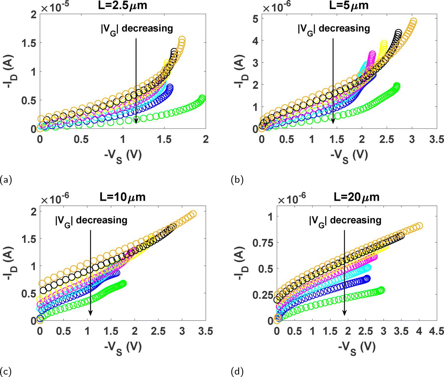
The output (ID–VD) and transfer (ID–VG) characteristics of the P3HT-based OTFTs are presented with symbols in Fig. 2 and solid lines in Fig. 3, respectively. The output characteristics in Fig. 2 were measured at a fast scan rate showing no hysteresis. The transfer characteristics of Fig. 3 were measured with a drain voltage of VD = −30 V, while the gate voltage VG was swept at a scan rate (SR) of 1000 mV s−1 (with VG steps of 0.1 V every 100 ms). Note that the transfer characteristics were measured close to the linear region to mitigate artifacts from contact resistance and gate-bias-dependent mobility. Saturation-region methods, which rely on square-law assumptions for their transfer characteristics, are prone to significant errors (overestimation and underestimation of carrier mobility) in disordered systems.46,47 P3HT devices fabricated on SiO2 dielectrics are known to operate reliably at gate voltages up to 100 V or more without significant deviation from ideal transistor behavior.48,49 In Fig. 2, the apparent absence of current saturation is attributed to short-channel effects, a well-documented phenomenon in organic transistors with reduced channel lengths.50 Among these, channel-length modulation plays a central role. The drift-based transport model introduced in Section 3 explicitly incorporates this effect through the channel-length modulation parameter, λ, ensuring a physically meaningful description of the output characteristics.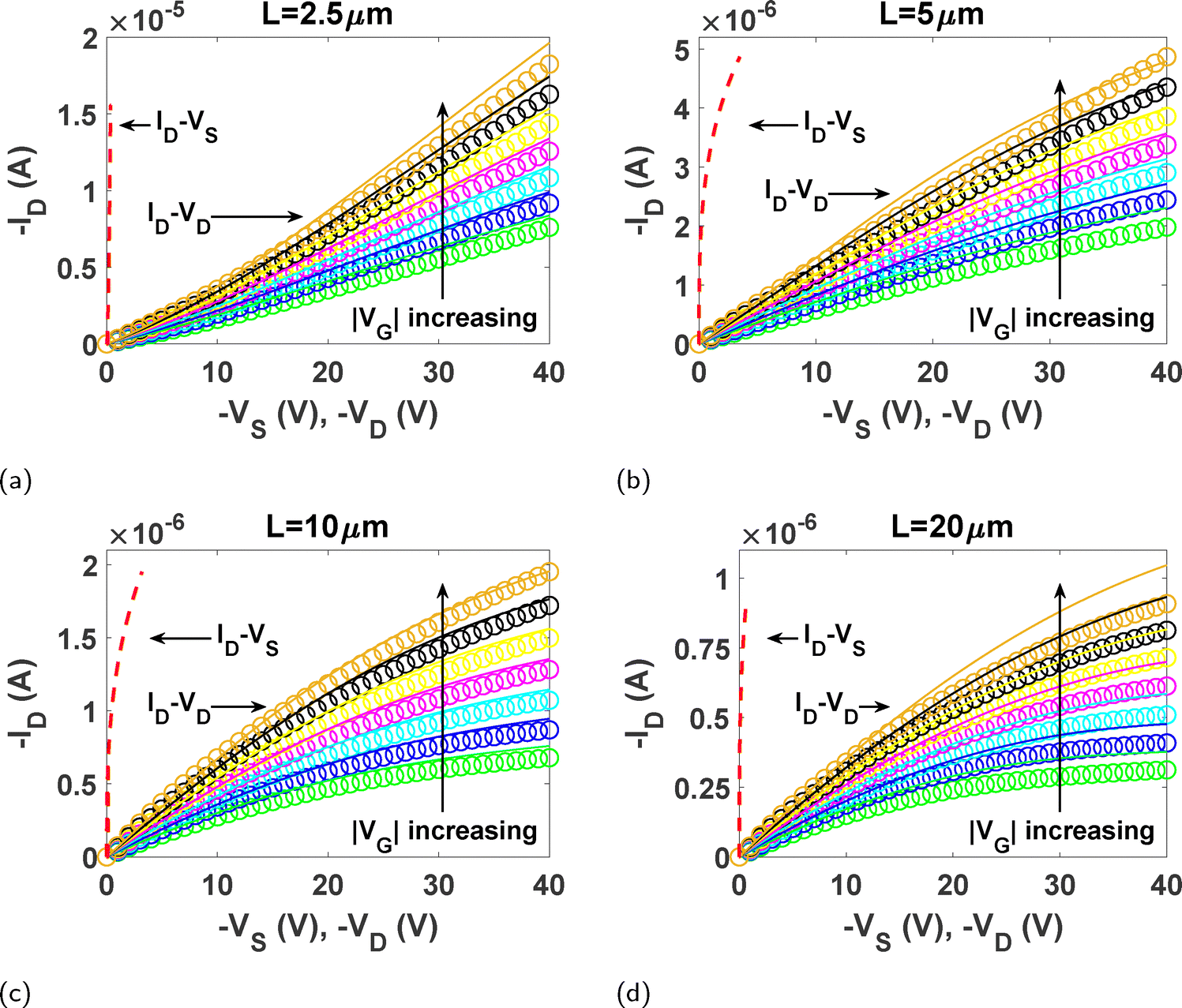 | ||
| Fig. 2 (a)–(d) Comparison of experimental output characteristics of P3HT based transistors with different channel lengths (symbols), with our calculations (solid lines), using the parameters of Table 1. VG is swept following this sequence of values: 0, −4, −8, −12, −16, −20 and −24 V. Close to the ordinate axis, the ID–VS curves at the contacts, calculated with eqn (3), are represented in dashed red lines. | ||
 | ||
| Fig. 3 (a)–(d) Comparison of experimental transfer characteristics (solid lines) for P3HT-based transistors with different channel lengths (Fig. 2) with simulated results (dashed lines) using parameters from Table 1. Time-dependent variables QtL (Fig. 5), VT (Fig. 6), and VSS (Fig. 7) were incorporated. OFF-to-ON voltage sweeps (black) and ON-to-OFF sweeps (blue) are shown. VD = −30 V. | ||
The transfer characteristics in Fig. 3a–d clearly exhibit a memory effect. Two distinct regions can be identified:
(i) loop-1 a closed hysteresis loop spanning most of the range for −VG (approximately −5 V to +18 V), and
(ii) loop-2 an open loop in the remaining measurement range for −VG (approximately −10 V to −5 V).
The behavior of closed loops like loop-1 has been extensively studied in previous research,51–54 including dynamic analyses.43 However, to our knowledge, the anomalous behavior observed in loop-2 has not been explored. Specifically, the origin of this second region, as well as the reduction in its size with increasing channel length (L), remains unexplained.
The combined analysis of these two loops in relation to the existence of traps in the transistor is the main objective of the work. We aim, not only to detect traps, but also to monitor the time evolution of the trapped charge density along the measurement of the transfer characteristics shown in Fig. 3. As the main tool for the dynamic characterization of OTFTs, we consider an unified compact model that describes the electrical characteristics of TFTs. It includes the effects of the intrinsic channel of the transistor, the source and drain contact regions, and a time-dependent threshold voltage VT(t) (Fig. 1a). The deduction of the complete model is detailed in ref. 43. For completeness, the key equations are summarized in the next section.
3 Generic drift model for OTFTs
3.1 Model for the intrinsic region
Organic thin-film transistors (OTFTs) are governed by charge transport mechanisms rooted in two widely accepted theories:(1) Charge drift in tail-distributed traps (TDTs)
(2) Variable range hopping (VRH)
A unifying feature of these models is the empirically observed relationship between mobility μ and gate voltage:
| μ = μ0(VG − VT)γ, | (1) |
 | (2) |
![[thin space (1/6-em)]](https://www.rsc.org/images/entities/char_2009.gif) exp[(VG − VT − V)/VSS], as well as the above-threshold regime, VEODR(VG,V) ≈ (VG − VT − V), with either V = VS or V = VD′, and VSS is the sub-threshold swing of the TFT.
exp[(VG − VT − V)/VSS], as well as the above-threshold regime, VEODR(VG,V) ≈ (VG − VT − V), with either V = VS or V = VD′, and VSS is the sub-threshold swing of the TFT.
The rest of the variables are VG, the gate terminal voltage, VD, the drain terminal voltage, and VS and VD′ are the values of the potential at the edges of the intrinsic channel in contact with the source and drain regions, respectively. Thus, VS is the voltage drop at the source contact and VDD′ = VD − VD′ is the voltage drop at the drain contact (Fig. 1a). Cox is the capacitance per unit area of the gate insulator and W and L are the channel width and length, respectively. L′ is the effective channel length modulated by the coefficient λ. If the channel length modulation effect is negligible, λ can be assumed zero and L′ ≈ L, minimizing the computational time of eqn (2). The model accounts for all transistor operating modes – linear, saturation, sub-threshold, and even reverse biasing. The success of eqn (2) lies in balancing physical interpretability with computational efficiency, making it a cornerstone for both device analysis and circuit simulation.
3.2 Model for the contact regions
To complement the intrinsic channel model (2), we incorporate a model that describes the electrical characteristics of the source and drain contact regions. While the intrinsic model already accounts for contact effects, drain contact effects are typically negligible in most OTFTs, as the potentiometry measurements showed in ref. 45. This simplification leads to VDD′ ≈ 0 V and VD ≈ VD′, meaning that only the source contact model is necessary.The source contact model, proven effective in various scenarios,41,42 can describe both space-charge-limited transport in low-energy contact barriers40 and injection-limited transport in Schottky barriers.61,68–70 The drain current ID is related to the voltage drop at the source contact VS by:
 | (3) |
| ID = VS/RS, | (4) |
The parameter MS in eqn (3) depends on the gate voltage40 as:
| MS = αs(VG − VT)1+γ, | (5) |
 | (6) |
Note that for staggered configurations, the voltage drop at the drain contact may be significant,62,76,77 requiring an additional model for the drain contact, as was detailed in ref. 42.
This generic drift model (2)–(6) is valid for static situations, but it does not account for trapping and de-trapping effects that cause the threshold voltage and sub-threshold swing to evolve over time. To address this, we incorporate models43 for these time-dependent effects, discussed below.
3.3 Dynamic behavior of the trapped charge density: VT(t) and VSS(t)
A shift in the threshold voltage ΔVT is linked to the variation of trapped charge density in the semiconductor or its interface with the insulator. This relationship78–80 is given by: | (7) |
Similarly, the sub-threshold swing VSS can change with the bulk or interface trapped charge density.16,81,82 Assuming the trap densities are energy-independent, VSS can be related to an equivalent trapped charge density QtL:16
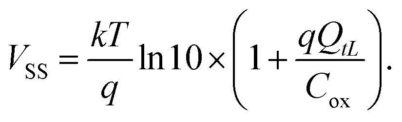 | (8) |
The variations in VSS are related to QtL by:
 | (9) |
The time-dependent behavior of VT and VSS at a particular instant tj can be related to their values at a previous instant tj−1 from eqn (7) and (9), respectively as:
 | (10) |
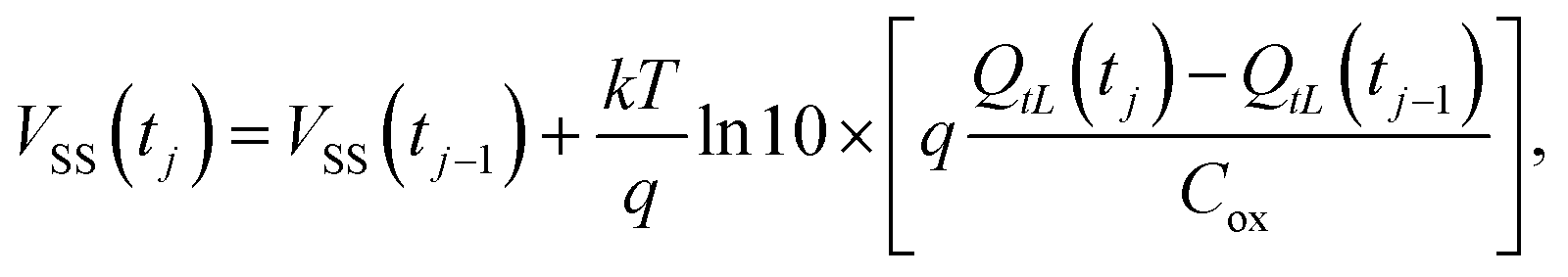 | (11) |
Second, our model explicitly incorporates the terminal voltage dependence of trap activity. The filling and emptying kinetics of both intrinsic and extrinsic traps are dynamically governed by the applied gate, VG, and drain, VD, voltages. This enables time-resolved analysis of charge trapping under operational conditions, revealing how transient voltage changes redistribute trapped charges over timescales spanning milliseconds to hours. By coupling spatial trap distributions with voltage-dependent kinetics, our framework captures critical phenomena such as bias-stress instability and hysteresis – key challenges in organic and hybrid transistor reliability.
This dual approach – linking trap microenvironments to macro-scale electrical behavior – provides a versatile tool for diagnosing degradation mechanisms and optimizing device stability across material systems.
The evolution of the trapped charge can be described with a first-order linear differential equation or a continuity equation for trapped charges (eqn (12)). One term is proportional to the trapped charge density and is controlled by a time constant τ. Another term is modeled as a generation term proportional to the drain current ID with a parameter β, where the flow of free charge carriers can be seen as a mechanism that favors the trapping:43
 | (12) |
Eqn (12) can be solved at discrete time intervals, allowing the calculation of the trapped charge QtL at a specific time tj for ntraps traps. Each trap has a unique time constant τr, with r = 1…ntraps:
 | (13) |
This equation applies to traps close to the intrinsic channel (denoted as b1), where variations in the trapped charge arise from changes in both VG and VD. Specifically, when VD ≠ 0 V and ID ≠ 0 A, the transistor transitions to a new steady state.
There are cases where the term βID in eqn (12) can be neglected. These include:
(i) VD = 0 V (i.e. ID = 0 A), or
(ii) Traps located far from the intrinsic channel, which are insensitive to the drain current – case (b2).
In these scenarios, the trapped charge QtL evolves towards a new steady state Qt0, at a rate governed by the time constant τ. The rate of change is described by:
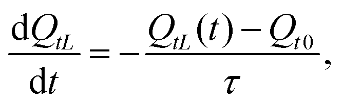 | (14) |
Eqn (14) can also be solved at discrete time intervals, allowing the calculation of QtL at each time tj for ntraps traps, with each trap having a different time constant τr:
 | (15) |
A detailed physical justification for the model described in eqn (12) and (14) can be found in ref. 43.
Finally, it is important to note that the drift model is developed for N-type TFTs, where ID, VD and VG are positive in the above-threshold region. In P-type TFTs, these quantities are typically negative. To account for this sign difference, the following steps are recommended:
(i) Change the sign of the experimental values for ID, VD and VG,
(ii) Apply the model equations as though the device were an N-type transistor,
(iii) After completing the analysis, reverse the signs of ID, VD and VG, as well as the resulting values of VT.
4 Results
4.1 Extraction of fitting parameters
This section aims to determine the value of the set of parameters necessary to evaluate all the equations of the model (2), (3), (10), (11), (13) and (15). An advanced fitting technique based on an evolutionary procedure is applied to the output characteristics ID–VD, represented by symbols in Fig. 2, and the ID–VG curves shown with solid lines in Fig. 3. The evolutionary procedure is outlined in Appendix A and the set of fitting parameters is named individual x (eqn (17)) in Appendix A.The procedure focuses on identifying common parameters across all four transistors, particularly those linked to the fabrication process, such as the mobility-related parameters μ0 and γ, as well as the threshold voltage VT and the early voltage per unit length  . The source contact region is modeled using the parameters ms and MS (eqn (3)). The effects of the contact region in OTFTs diminish with increasing channel length.83,84 As shown in Fig. 2, the experimental ID–VD curves evolve from concave to convex at low drain voltages as the channel length L increases. For L = 2.5 μm, a distinct concave behavior at low VD indicates a space charge limited current (SCLC) regime, characteristic of short-channel transistors. This behavior suggests that the evolutionary procedure will be sensitive to the concave–convex transition, providing distinct values for ms based on channel length.
Despite this, the voltage drop across the contact region should remain similar for all transistors, as the fabrication process is uniform, with only L varying. The differences in ms should be balanced by adjusting MS. It is important to note that shorter channel lengths result in lower ID values for the same bias point. For a quadratic relationship between ID and VD in the contact region, the slope of this curve decreases at lower ID, revealing information about the contact conductance, which is linked to MS (eqn (3)).
From an analytical perspective, the parameter extraction procedure may yield higher values of MS for shorter channels, compensating for the increased ms. A crucial check will be whether the voltage drop across the contact region remains consistent across the four transistors.
The variation in threshold voltage depends on the evolution of the trap charge density (eqn (7)). However, the initial value of VT(0) is unknown and depends on the experimental conditions. Before conducting both ID–VG and ID–VD experiments, the samples are held at the same gate voltage, VG = 10 V. Thus, VT(0) is assumed to be the same in both experiments. Once the experiments commence (t > 0), VT(t) remains constant throughout the ID–VD experiment, while it evolves with changes in the trap charge density (eqn (10)) during the transfer characteristics.
Initially, only one type of trap, with charge density QtL,1, is considered. Since the procedure evaluates charge density increments during ID–VG experiments, we assume an arbitrary initial value of QtL,1(0) = 0 C cm−2. As −VG varies from −10 to +18 V, it increases the number of free charge carriers (holes) in the conducting layer, causing the traps to become positively charged. If the analysis detects additional traps, their charge densities (QtL,2(0),…,QtL,ntraps(0)) will be included in the set of fitting parameters x (eqn (17)).
Other parameters related to the traps include the time constant τ and the factor β. The time constant τ is specific to the type of trap, but remains consistent across the four transistors. The parameter β, which modulates the drain current (eqn (12)), is dependent on the local electric field along the channel, as described in ref. 43. For this reason, it is preferable to treat β as distinct for each transistor and, if necessary, separate the forward and reverse sweeps in the transfer characteristics (βrf and βrb, respectively, for trap #r).
The sub-threshold swing VSS is sensitive to the trap charge density (eqn (8)) and its variation (eqn (9)). Determining the initial value VSS(0) provides insights into the trapped charge density, which we assumed to be QtL,1(0) = 0 C cm−2. VSS is typically extracted from the slope of the ID–VG curve in the sub-threshold region. However, our procedure can extract it from ID–VG curves above threshold, as the generic drift model (2) is highly sensitive to this parameter at any bias point. VSS offers information about various traps:
(i) Traps formed during fabrication, whose density is assumed constant across different L, and
(ii) Traps created unintentionally, whose density may vary depending on the length of the transistor or exposure to external conditions.
4.2 Steps
After classifying parameters as either common or varying across transistors PD ∈ {ms,MS,VSS(0),βrf,βrb} in the four sets of transistors, the extraction procedure proceeds as follows:
• Step 1: estimate parameters μ0, γ, VT and  by analyzing the current characteristics of the four transistors using the traditional MOS model41,42,58,59,85,86 and the HVG method.87
• Step 2: define the initial search space for all parameters in the set x (eqn (17)), considering only one type of trap (r = 1), with parameters τ1, β1f and β1b, and QtL,1(0) = 0 C cm−2.
• Step 3: run the evolutionary procedure on the four transistors. For brevity, the initial fitting results for the L = 5 μm transistor are shown in Fig. 4a (parameters in Table 2). This channel length was selected as a representative case to balance clarity and comprehensiveness, that is, to avoid extreme scaling effects (e.g., pronounced contact resistance in shorter channels or bulk-limited transport in longer channels) while capturing the core behavior of the system. The following observations are entirely applicable to the other three transistors. The fitting errors (eqn (19)) are O1 = 16.06% and O2 = 7.87%. Despite a good overall fit, loop-2, corresponding to the lowest values of −VG, remains poorly fitted. This suggests the presence of a second trap (#2), which influences loop-2 behavior. The analysis of loop-2 in Fig. 4a reveals an exponential transient at the start of the forward sweep (FS), consistent with the evolution of trapped charge density. This transient can be explained with a trapped charge density evolving like in eqn (15) with an initial charge QtL,2(0) and final steady state Qt0,2 = 0 C cm−2, i.e. QtL,2(t) = QtL,2(0)exp(−t/τ2). Accordingly, in this experiment the threshold voltage at t = 0 s must be initialized, not at VT(0), but at VT(0) − QtL,2(0)/Cox. Identical trends were observed across all devices, confirming the universal applicability of our model.
 | ||
| Fig. 4 Comparison of the experimental transfer characteristics of the P3HT based transistor with L = 5 μm (solid lines; shown also in solid lines in Fig. 3b), with our calculations (dashed lines). (a) The extraction procedure and calculation considers an individual (eqn (17)) with only one trap. The values of the parameters are in Table 2. (b) The extraction procedure considers an individual (eqn (17)) with two traps. The values of the parameters are in Table 1. Later, the ID–VG curve is calculated with only one trap. The voltage sweep from OFF-to-ON is in black lines and from ON-to-OFF in blue lines. VD = −30 V. | ||
• Step 4: add trap #2 to the set x (eqn (17)), including the initial charge density QtL,2(0) and time constant τ2, then rerun the evolutionary procedure for improved fits.
• Step 5: analyze parameter values in the set x (eqn (17)). For common parameters PC, calculate the average (〈PC〉) and deviations (ΔP) across the four transistors. Refine the search space by reducing the range of PC to [〈PC〉 − ΔP, 〈PC〉 + ΔP] and repeat until acceptable convergence is reached. Parameters that do not converge to common values, such as ms, MS, VSS(0), β1f, β1b, QtL,2(0) are analyzed individually.
The best fit results from the procedure outlined in Appendix A are shown in Fig. 2 (solid lines for ID–VD curves) and Fig. 3 (dashed lines for ID–VG curves). The corresponding fitting parameters are summarized in Table 1. The extracted mobility (μ0 = (3.01 ± 0.02) × 10−5 cm2 (V s)−1), mobility enhancement factor (γ = 0.25), threshold voltage (VT = 35 ± 2 V), Early voltage per unit length  , and time constants (τ1 = 2 s, and τ2 = 1.3 s) reflect mean values and their deviations (within the range 〈PC〉 ± ΔP) across all channel lengths. That is, the actual values for these common parameters should be located in an interval defined by their mean value 〈PC〉 and their deviation ±ΔP. The observed deviations lie within expected tolerances for disordered semiconductors, underscoring the model's robustness to fabrication variability. The extracted values of the early voltage per unit length
  confirm the presence of short-channel effects, as predicted in Section 2.2. These effects begin to manifest in devices with a channel length of approximately 10 μm, and become increasingly pronounced as the channel length is reduced to 2.5 μm, consistent with the onset of channel pinch-off and modulation effects. The remaining parameters exhibit clear dependence on L, as detailed in Table 1. Further analysis of the trapped charge density (QtL(t)), threshold voltage (VT(t)), and sub-threshold swing (VSS(t)) (see Fig. 5–7) is presented in the next section.
 is in V cm−1, QtL,2 is in C cm−2, τ1 and τ2 are in s, VT is in V and VSS is in V – QtL,1(0) = 0 C cm−2 in the four cases – checked boxes indicate the experiment is aimed to fit
| x | Value | Fitting | ||||
|---|---|---|---|---|---|---|
| L = 2.5 μm | L = 5 μm | L = 10 μm | L = 20 μm | I D–VD | I D–VG | |
| x 1 = μ0 | 3.00 × 10⁻⁵ | 3.00 × 10⁻⁵ | 3.00 × 10⁻⁵ | 3.03 × 10⁻⁵ | ⊠ | ⊠ |
| x 2 = γ | 0.25 | 0.25 | 0.25 | 0.25 | ⊠ | ⊠ |
| x 3 = VT | 37.48 | 34.83 | 32.62 | 35.89 | ⊠ | ⊠ |
| x 4 = VSS | 22.01 | 22.44 | 13.04 | 3.53 | ⊠ | ⊠ |
| x 5 = ms | 1.76 | 0.30 | 0.34 | 0.30 | ⊠ | ⊠ |
| x 6 = MS | 1.00 × 10⁻⁴ | 3.34 × 10⁻⁶ | 1.32 × 10⁻⁶ | 1.04 × 10⁻⁶ | ⊠ | ⊠ |

|
92819 |
118164 |
90466 |
100344 |
⊠ | ⊠ |
| x 8 = β1f | −1.23 × 10⁻¹⁰ | −1.00 × 10⁻¹⁰ | −1.17 × 10⁻⁷ | −1.42 × 10⁻⁷ | □ | ⊠ |
| x 9 = β1b | −1.05 × 10⁻³ | −3.49 × 10⁻³ | −8.45 × 10⁻³ | −1.97 × 10⁻² | □ | ⊠ |
| x 10 = τ1 | 2 | 2 | 2 | 2 | □ | ⊠ |
| x 11 = τ2 | 1.3 | 1.3 | 1.3 | 1.3 | □ | ⊠ |
| x 12 = QtL,2(0) | 11.9 × 10⁻⁸ | 12.0 × 10⁻⁸ | 8.74 × 10⁻⁸ | 5.43 × 10⁻⁸ | □ | ⊠ |
| x | Value |
|---|---|
| x 1 = μ0 | 6.32 × 10⁻⁵ cm2 V−1 s−1 |
| x 2 = γ | 0.0 |
| x 3 = VT | 37.58 V |
| x 4 = VSS | 8.46 V |
| x 5 = ms | 0.78 |
| x 6 = MS | 3.17 × 10⁻⁵ A V(−2−γ) |

|
119995 V cm−1 |
| x 8 = β1f | −4.15 × 10⁻⁹ |
| x 9 = β1b | −3.20 × 10⁻³ |
| x 10 = τ1 | 1.8034 s |
 | ||
| Fig. 5 (a)–(d) Time evolution of QtL (trapped charge density) calculated using eqn (13) and (15) and the parameters of Table 1 during the measurements of the transfer characteristics of P3HT based transistors with different channel lengths in Fig. 3. | ||
 | ||
| Fig. 6 (a)–(d) Time evolution of VT (threshold voltage) calculated from eqn (10) and the parameters of Table 1 during the measurements of the transfer characteristics of P3HT based transistors with different channel lengths in Fig. 3. | ||
 | ||
| Fig. 7 Time evolution of VSS (sub-threshold swing) computed viaeqn (11) and the parameters of Table 1 during the measurements of the transfer characteristics of P3HT based transistors with different channel lengths in Fig. 3. | ||
4.3 Discussion
Fig. 5 highlights two distinct regions: the initial transient, occurring during the first 10 seconds, which corresponds to QtL,2(t), and the subsequent region, corresponding to QtL,1(t). To isolate the effect of trap #2, the ID–VG curve for L = 5 μm (previously shown with dashed lines in Fig. 3b) was recalculated with the same parameter values from Table 1, except that QtL,2(0) = 0 C cm−2. The result is depicted with dashed lines in Fig. 4b and compared with experimental data (solid line). When trap #2 is neglected, our calculations match the experimental data in loop-1 but not in loop-2. Specifically, if trap #2 is absent, no transient response is observed at the beginning of the forward sweep (dashed black line in Fig. 4b). A similar behavior is reported in Fig. 2 of ref. 88, where OTFT transfer characteristics with and without self-assembled monolayers (SAMs) are shown. Their transfer characteristics measurements without SAMs exhibit a transient behavior similar to ours, while no such behavior is detected with SAMs.The trapped charge density variation in trap #2, represented by QtL,2(0), decreases as L increases (see Fig. 5 and Table 1). The maximum variation of the trapped charge density in trap #1, ΔQtL,1max, remains independent of L, fluctuating around ΔQtL,1max = (2.0 ± 0.3) × 10−8 C cm−2, which is smaller than the variation in trap #2. The trapped charge density variations in the ID–VG curves (Fig. 5) affect both VT (Fig. 6) and VSS (Fig. 7). It is important to note that the generic charge drift model (2) is highly sensitive to the values of these two parameters. Although the measurements do not cover the sub-threshold region, even small variations in VSS can significantly impact the fit to experimental data.
In addition to QtL,2(0), VSS(0) also shows a clear decrease as L increases. Using the values of VSS(0) in eqn (8), we estimate the global trap charge density Nt = Nt,1 + Nt,2 in the transistor, where Nt,1 and Nt,2 correspond to traps #1 and #2, respectively. The resulting values of Nt are provided in Table 3 and illustrated in Fig. 8 as a function of the maximum trapped charge density variation in trap #2, ΔNtL2 = QtL,2(0)/q. A proportional relationship is observed in Fig. 8, where only 2–8% of the total trapped charge varies during the experiment. These values suggest that trap #1 is present with constant concentration across all four transistors, likely related to the fabrication process. In contrast, the trapped charge density and its variation in trap #2 clearly depend on the channel length of the transistor, and can be related to unexpected traps originated from environmental species.
| L (μm) | N t (cm−2) | ΔNtL2 (cm−2) |
|---|---|---|
| 2.5 | 3.46 × 10¹³ | 7.45 × 10¹¹ |
| 5 | 3.53 × 10¹³ | 7.53 × 10¹¹ |
| 10 | 2.05 × 10¹³ | 5.47 × 10¹¹ |
| 20 | 5.48 × 10¹² | 3.39 × 10¹¹ |
 | ||
| Fig. 8 Relation between the value of the density of trapped charges Nt in the transistor, extracted from the parameter VSS and eqn (9), and the maximum variation of the density of trapped charges in trap #2, determined as ΔNtL2 = −QtL,2(0)/q, as a function of the channel length. | ||
Li and colleagues89 investigated the humidity dependence of electrical performance in different OTFTs, showing that moisture sensitivity varies with channel length. They attributed performance degradation under high relative humidity (RH) to charge trapping at grain boundaries by polar water molecules. In our study, assuming the same concentration of environmental molecules (e.g., humidity, atmospheric contaminants) surrounding all transistors, the trap density will be higher in transistors with smaller volumes and shorter lengths. Specifically, the surface area exposed to the environment, including source and drain fingers and the organic channel, increases 1.8 times from the shortest (2.5 μm) to the longest (20 μm) channel transistor (Fig. 1b). The exposed surface area of the organic channel increases eightfold, enhancing interactions with environmental species. Assuming absorption of environmental molecules by the organic channel, this results in a 4.5-fold increase in potential trap density from the shortest to the longest channel transistor. This observation aligns with the factor of 6.3 derived from Nt values in Table 3.
A final observation regarding the size of the hysteresis loops in the transfer curves of Fig. 3 concerns the initial gate voltage VG (VG ≥ 10 V), which is intentionally selected. This starting point ensures that no free carriers are present to occupy the fabrication-induced trap states (referred to as trap #1). As a result, the initial trapped charge density for these states is set to zero, i.e., QtL,1(0) = 0 C cm−2. In contrast, the initial occupancy of trap #2, associated with unexpected traps introduced by environmental species, depends on external factors such as the concentration of environmental molecules and the effective device surface area exposed to ambient conditions. Consequently, the corresponding initial charge density, QtL,2(0), and hence the observed open-loop hysteresis in the transfer curves of Fig. 3, are primarily influenced by these environmental conditions and are not expected to depend on the initial value of VG.
As noted above, the different values of ms and MS extracted for the four transistors, which model the contact region, warrant further analysis. For practical reasons, MS is assumed to be constant across all values of VG. However, MS can vary with VG as shown in eqn (5). This simplification may lead to less accurate fits between calculations and experimental data, as seen in Fig. 2d (solid lines and symbols). Nevertheless, useful qualitative insights and qualitative information can still be gained from ms and MS. The value of ms primarily reflects the concave or convex shape of the ID–VD curves. For L = 2.5 μm, ms = 1.75 suggests a nearly quadratic ID–VS relation in the contact region, operating in the SCLC regime. For the other three transistors, ms < 1, indicating convex shapes in the output characteristics (Fig. 2b–d). To compensate for the smaller ms values in these cases, MS decreases as L increases, as discussed in Section 4.1. The resulting ID–VS curves are represented by dashed red lines in Fig. 2a–d.
To refine our understanding of the contact region and improve agreement between calculations and experimental data, we proceed with an additional step: calculating the contact voltage VS from eqn (2) as:
 | (16) |
 | ||
| Fig. 9 (a)–(d) ID–VS curves at the contacts extracted from eqn (16), in which the experimental values of the P3HT based transistors with different channel lengths shown in Fig. 2, and the parameters of Table 1 are introduced. | ||
Notably, the voltage drop across the source contact region remains consistent (∼1–2 V) across all channel lengths (Fig. 9), underscoring its independence from device geometry and reinforcing the contact-limited nature of the transition. While minor irregularities in the curves reflect experimental noise inherent to direct data extraction, the overarching trend remains robust. This phenomenon mirrors observations in ammonia gas sensors,41 where adsorbed gas molecules modulate interfacial barriers, inducing analogous curvature changes in ID–VS characteristics. Such parallels highlight the broader relevance of interfacial trap dynamics in organic and hybrid electronic systems, offering insights for designing stable, high-performance devices.
Further, the principles governing trap #2 are not confined to organic systems but apply to a broad spectrum of hybrid and emerging semiconductor technologies. For instance, in oxide-based TFTs (e.g., InGaZnO), interfacial traps at dielectric–semiconductor boundaries similarly dictate bias-stress instability, a critical concern in display electronics.92 Likewise, perovskite transistors – a rising star in optoelectronics – suffer from ion migration and interfacial defect formation, phenomena that align seamlessly with our charge-trapping model.93 Even in crystalline systems, where traps are less prevalent, the framework retains utility by simplifying to classical models under low-disorder conditions, bridging the gap between traditional and next-generation semiconductors.25
• Performing measurements in the sub-threshold region, though this is not strictly necessary.
• Measurements at different scan rates could aid in the characterization process.
• Possibly use slower scan rates that would reveal hysteresis in the output characteristics, though this would complicate the analysis as VT and VSS would vary over time.43
• Combining measurements from encapsulated and non-encapsulated transistors, or conducting measurements under varying environmental conditions (e.g., reduced humidity or a nitrogen atmosphere), would also help in future characterization efforts.
• In this work, no additional time-dependent measurements were necessary to detect the traps. However, if traps with significantly different lifetimes were present, the additional transient current measurements in response to voltage pulses would be required.51
5 Conclusions
A novel approach to analyzing the current characteristics in OTFTs was proposed, emphasizing the importance of important details to extract information about traps. This approach employs an evolutionary parameter extraction procedure, based on a compact model that evaluates the drain current and accounts for the dynamic evolution of both the threshold voltage and trapped charge density in OTFTs. The procedure was tested using current characteristics with hysteresis measured in P3HT-based transistors with varying channel lengths.By analyzing the time evolution of the threshold voltage during the voltage sweep in the transfer characteristics, we were able to detect the presence of different types of traps. Typical hysteresis loops in the transfer characteristics were attributed to traps created during the fabrication process, with a concentration that remains independent of the channel length. In contrast, anomalous loops observed in the experimental data were interpreted as arising from a second type of trap. The number of trapped charges and their variation associated with this second type of trap both depend on the channel length and exhibit a linear relationship. This suggests that these unexpected traps originate from environmental species (e.g., adsorbed water or oxygen), being absorbed into different volumes of the semiconductor and resulting in varying trapped charge densities.
Author contributions
J. A. Jiménez-Tejada: writing – review & editing, writing – original draft, validation, supervision, project administration, methodology, investigation, conceptualization. A. Romero: writing – review & editing, writing – original draft, visualization, software, methodology, formal analysis, data curation. S. Mansouri: data curation, methodology, resources, supervision, validation, visualization, writing – review & editing. M. Erouel: data curation, resources, supervision, validation, visualization. L. El Mir: data curation, resources, supervision, validation, visualization. M. J. Deen: writing – review & editing, validation, investigation.Data availability
The data supporting this article have been included as part of the ESI.†Conflicts of interest
There are no conflicts to declare.Appendix A: evolutionary parameter extraction procedure
This appendix introduces an advanced fitting technique based on an evolutionary procedure. It is designed to reduce the workload of the expert or decision maker (DM) during parameter extraction. This method has been successfully applied to the characterization of thin-film transistors (TFTs) in both static41,42,59,85,101,102 and dynamic regimes, including current transients and hysteretic current characteristics.43 The analyses are conducted using the open-source evolutionary tool ECJ (A Java-based Evolutionary Computation Research System).103 In this work, the evolutionary parameter extraction procedure is adapted to extract trap-related information from transfer characteristics with hysteresis, as well as from abnormal behavior observed at low gate voltages (loop-2). The key steps of the adapted procedure are outlined in the following subsections.A.1 Individual representation (set of fitting parameters)
The evolutionary procedure defines the “individual” of the population, denoted by x, which represents the set of fitting parameters necessary to calculate all equations in the model (2), (3), (10), (11), (13) and (15): | (17) |
Here, r = 1,…,ntraps; ntraps represents the various trap types or total number of traps; and  is the early voltage per unit length. The terms VT(0) and VSS(0) correspond to the initial values of VT(t) and VSS(t) for a specific experiment.
A.2 Measurement discretization and timing
Initially, the experimental ID data, measured during the output or transfer characteristics, must be linked to the time instances tj at which each measurement is taken. Specifically, ID = ID(VG(tj),VD(tj)), where j ∈![[Doublestruck Z]](https://www.rsc.org/images/entities/char_e17d.gif) , with 1 ≤ j ≤ tN, and tN represents the total number of discrete time values. The measurement protocol is as follows:
, with 1 ≤ j ≤ tN, and tN represents the total number of discrete time values. The measurement protocol is as follows:
(1) Transfer characteristics:
• VD = −30 V
• VG(tj) = VG(tj−1) ± SR × (tj − tj−1), where SR = 1000 mV s−1 and (tj − tj−1) = 100 ms.
The positive sign corresponds to the forward sweep (FS) (sweeping −VG from −10 to 18 V), while the negative sign corresponds to the backward sweep (BS) (sweeping −VG from 18 to −10 V).
(2) Output characteristics:
• VD(tj) = VD(tj−1) + SR × (tj − tj−1) with −VD ∈ [0,40] V
• VG remains fixed at values such as 0 V, −4 V, −8 V, −12 V, −16 V, −20 V, or −24 V.
• SR and (tj − tj−1) can vary, as no hysteresis is detected.
• VG is held for several seconds at VD = 0 V to stabilize the trapped charge, and then VD is swept with a large SR.
The numerical estimation of ID, calculated using our model (2), (3), (10), (11), (13) and (15), is denoted by  .
.
A.3 Fitness function
The evolutionary parameter extraction procedure is applied independently to each of the four transistors with varying channel lengths. For each case, it solves a multi-objective optimization problem (MOP)85 with two objectives• O1: output characteristics
• O2: transfer characteristics
Both objectives aim to minimize the error Ok, where k = 1, 2, between the experimental values ID = ID(VG(tj),VD(tj)) and the model-based estimations  .
.
The normalized root mean squared error (NRMSE) is used to quantify the errors for both objectives:104
 | (18) |
Thus, our MOP, denoted as O, is defined as O = (O1,O2), where
 | (19) |
These objectives ensure that we accurately reproduce the experimental ID–VD and ID–VG curves by optimizing the parameters encoded in x within the model.
Acknowledgements
The authors acknowledge support from the project PID2022-139586NB-C44 funded by MCIN/AEI/10.13039/501100011033 and by European Union NextGenerationEU/PRTR.References
- T. Jiang, Y. Wang, Y. Zheng, L. Wang, X. He, L. Li, Y. Deng, H. Dong, H. Tian and Y. Geng, et al. , Nat. Commun., 2023, 14, 2281 CrossRef CAS.
- L. Chen, T. K. Maiti, H. Miyamoto, M. Miura-Mattausch and H. J. Mattausch, IEICE Trans. Fundam. Electron. Commun. Comput. Sci., 2016, E99.A, 798–805 CrossRef.
- K.-L. Han, J.-H. Han, B.-S. Kim, H.-J. Jeong, J.-M. Choi, J.-E. Hwang, S. Oh and J.-S. Park, ACS Appl. Mater. Interfaces, 2019, 12, 3784–3791 CrossRef.
- S. Kim, J. Seo, T. Park and H. Yoo, Adv. Electron. Mater., 2022, 8, 2200752 CrossRef CAS.
- A. Campos, S. Riera-Galindo, J. Puigdollers and M. Mas-Torrent, ACS Appl. Mater. Interfaces, 2018, 10, 15952–15961 CrossRef CAS PubMed.
- I.-Y. Jo, D. Jeong, Y. Moon, D. Lee, S. Lee, J.-G. Choi, D. Nam, J. H. Kim, J. Cho, S. Cho, D.-Y. Kim, H. Ahn, B. J. Kim and M.-H. Yoon, Adv. Mater., 2024, 36, 2307402 CrossRef CAS PubMed.
- H. F. Haneef, A. M. Zeidell and O. D. Jurchescu, J. Mater. Chem. C, 2020, 8, 759–787 RSC.
- S. Hou, H. Fan, M. Wu, X. Yu and J. Yu, Sci. China: Technol. Sci., 2021, 64, 1057–1064 CrossRef CAS.
- M. Jang, S. K. Kim, J. Lee, S. Ji, W. Song, S. Myung, J. Lim, S. S. Lee, H.-K. Jung, J. Lee and K.-S. An, J. Mater. Chem. C, 2019, 7, 14504–14510 RSC.
- J. Zhu, X. Wang and H. Wang, J. Electron. Mater., 2020, 49, 4691–4696 CrossRef CAS.
- B. Nketia-Yawson, A.-R. Jung, Y. Noh, G.-S. Ryu, G. D. Tabi, K.-K. Lee, B. Kim and Y.-Y. Noh, ACS Appl. Mater. Interfaces, 2017, 9, 7322–7330 CrossRef CAS.
- M. Deen and M. Kazemeini, Proc. IEEE, 2005, 93, 1312–1320 CAS.
- N. Qiao, P. Wei, Y. Xing, X. Qin, X. Wang, X. Li, L. Bu, G. Lu and Y. Zhu, Adv. Mater. Interfaces, 2022, 9, 2200713 CrossRef CAS.
- S. Anand, K. P. Goetz, Z. A. Lamport, A. M. Zeidell and O. D. Jurchescu, Appl. Phys. Lett., 2019, 115, 073301 CrossRef.
- J. Dacuña and A. Salleo, Phys. Rev. B: Condens. Matter Mater. Phys., 2011, 84, 195209 CrossRef.
- W. L. Kalb and B. Batlogg, Phys. Rev. B: Condens. Matter Mater. Phys., 2010, 81, 035327 CrossRef.
- T. He, Y. Wu, G. D'Avino, E. Schmidt, M. Stolte, J. Cornil, D. Beljonne, P. P. Ruden, F. Würthner and C. D. Frisbie, Nat. Commun., 2018, 9, 2141 CrossRef.
- M. J. Deen and F. Pascal, Electrical Characterization of Semiconductor Materials and Devices, in Springer Handbook of Electronic and Photonic Materials, ed. S. Kasap and P. Capper, Springer Science and Business Media Inc., New York, 2006, pp. 409–438 Search PubMed.
- M. J. Deen and F. Pascal, J. Mater. Sci.: Mater. Electron., 2006, 17, 549–575 CrossRef CAS.
- R. Giridharagopal, P. A. Cox and D. S. Ginger, Acc. Chem. Res., 2016, 49, 1769–1776 CrossRef CAS.
- F. Bussolotti, J. Yang, M. Hiramoto, T. Kaji, S. Kera and N. Ueno, Phys. Rev. B: Condens. Matter Mater. Phys., 2015, 92, 115102 CrossRef.
- D. P.-K. Tsang, T. Matsushima and C. Adachi, Sci. Rep., 2016, 6, 26921 Search PubMed.
- M. Deen, O. Marinov, S. Holdcroft and W. Woods, IEEE Trans. Electron. Dev., 2001, 48, 1688–1695 CrossRef CAS.
- O. Marinov, M. Deen, J. Yu, G. Vamvounis, S. Holdcroft and W. Woods, IEE Proc. Circuits Devices Syst., 2004, 151, 466 Search PubMed.
- O. Marinov, M. J. Deen and J. A. Jiménez-Tejada, Phys. Rep., 2022, 990, 1–179 Search PubMed.
- Z. A. Lamport, H. F. Haneef, S. Anand, M. Waldrip and O. D. Jurchescu, J. Appl. Phys., 2018, 124, 071101 CrossRef.
- W. L. Kalb, K. Mattenberger and B. Batlogg, Phys. Rev. B: Condens. Matter Mater. Phys., 2008, 78, 035334 CrossRef.
- G. Horowitz, R. Hajlaoui and P. Delannoy, J. Phys. III, 1995, 5, 355–371 CrossRef CAS.
- D. V. Lang, X. Chi, T. Siegrist, A. M. Sergent and A. P. Ramirez, Phys. Rev. Lett., 2004, 93, 086802 CrossRef CAS PubMed.
- G. Fortunato, D. B. Meakin, P. Migliorato and P. G. Le Combers, Philos. Mag. B, 1988, 57, 573–586 CAS.
- V. V. Brus, C. M. Proctor, N. A. Ran and T.-Q. Nguyen, Adv. Energy Mater., 2016, 6, 1502250 CrossRef.
- L. Zhang, H. Nakanotani and C. Adachi, Appl. Phys. Lett., 2013, 103, 093301 CrossRef.
- H. Hirwa, S. Pittner and V. Wagner, Org. Electron., 2015, 24, 303–314 CrossRef CAS.
- H. Hatta, Y. Miyagawa, T. Nagase, T. Kobayashi, T. Hamada, S. Murakami, K. Matsukawa and H. Naito, Appl. Sci., 2018, 8, 1493 CrossRef.
- L. Xu, J. Wang and J. W. P. Hsu, Phys. Rev. Appl., 2016, 6, 064020 CrossRef.
- P. P. Boix, G. Garcia-Belmonte, U. Muñecas, M. Neophytou, C. Waldauf and R. Pacios, Appl. Phys. Lett., 2009, 95, 233302 CrossRef.
- K. Kuribara, H. Wang, N. Uchiyama, K. Fukuda, T. Yokota, U. Zschieschang, C. Jaye, D. Fischer, H. Klauk and T. Yamamoto, et al. , Nat. Commun., 2012, 3, 723 CrossRef PubMed.
- X. Jia, C. Fuentes-Hernandez, C.-Y. Wang, Y. Park and B. Kippelen, Sci. Adv., 2018, 4, eaao1705 CrossRef PubMed.
- O. Marinov, M. J. Deen, U. Zschieschang and H. Klauk, IEEE Trans. Electron Devices, 2009, 56, 2952–2961 Search PubMed.
- J. A. Jiménez-Tejada, J. A. López-Villanueva, P. López-Varo, K. M. Awawdeh and M. J. Deen, IEEE Trans. Electron Devices, 2014, 61, 266–277 Search PubMed.
- A. Romero, J. González, M. Deen and J. A. Jiménez-Tejada, Org. Electron., 2020, 77, 105523 CrossRef CAS.
- A. Romero, J. Jiménez-Tejada, J. González and M. Deen, Org. Electron., 2021, 92, 106129 CrossRef CAS.
- A. Romero, J. Jiménez-Tejada, R. Picos, D. Lara, J. Roldán and M. Deen, Org. Electron., 2024, 129, 107048 CrossRef CAS.
- M. Ba, S. Mansouri, A. Jouili, Y. Yousfi, L. Chouiref, M. Jdir, M. Erouel, F. Yakuphanoglu and L. E. Mir, J. Electron. Mater., 2022, 52, 1203–1215 CrossRef.
- L. Bürgi, T. J. Richards, R. H. Friend and H. Sirringhaus, J. Appl. Phys., 2003, 94, 6129–6137 CrossRef.
- O. Marinov, M. J. Deen, C. Feng and Y. Wu, J. Appl. Phys., 2014, 115, 034506 CrossRef.
- C. Liu, G. Li, R. Di Pietro, J. Huang, Y.-Y. Noh, X. Liu and T. Minari, Phys. Rev. Appl., 2017, 8, 034020 CrossRef.
- A. Jouili, S. Mansouri, A. A. Al-Ghamdi, L. El Mir, W. A. Farooq and F. Yakuphanoglu, J. Electron. Mater., 2016, 46, 2221–2231 CrossRef.
- S. Mansouri, B. Coskun, L. El Mir, A. G. Al-Sehemi, A. Al-Ghamdi and F. Yakuphanoglu, J. Electron. Mater., 2018, 47, 2461–2467 CrossRef CAS.
- J. N. Haddock, X. Zhang, S. Zheng, Q. Zhang, S. R. Marder and B. Kippelen, Org. Electron., 2006, 7, 45–54 CrossRef.
- C. Ucurum, H. Goebel, F. A. Yildirim, W. Bauhofer and W. Krautschneider, J. Appl. Phys., 2008, 104, 084501 CrossRef.
- D. K. Hwang, M. S. Oh, J. M. Hwang, J. H. Kim and S. Im, Appl. Phys. Lett., 2008, 92, 013304 CrossRef.
- D. I. Kim, N. Y. Kwon, S.-H. Lee, M. J. Cho, J. Kim, D. H. Choi and J. Joo, Org. Electron., 2022, 108, 106599 CrossRef CAS.
- L. Karunakaran, P. K. Manda and S. Dutta, Org. Electron., 2019, 65, 15–18 CrossRef CAS.
- O. Marinov, M. J. Deen and R. Datars, J. Appl. Phys., 2009, 106, 064501 CrossRef.
- M. J. Deen, O. Marinov, U. Zschieschang and H. Klauk, IEEE Trans. Electron Devices, 2009, 56, 2962–2968 CAS.
- M. Fayez, K. M. Morsi and M. N. Sabry, IET Circuits Devices Syst., 2017, 11, 409–420 CrossRef.
- A. Romero, J. González, R. Picos, M. J. Deen and J. A. Jiménez-Tejada, Org. Electron., 2018, 61, 242–253 CrossRef CAS.
- A. Romero, C. Jiménez, J. González, P. López-Varo, M. J. Deen and J. A. Jiménez-Tejada, Org. Electron., 2019, 70, 113–121 CrossRef CAS.
- S. Abdinia, F. Torricelli, G. Maiellaro, R. Coppard, A. Daami, S. Jacob, L. Mariucci, G. Palmisano, E. Ragonese, F. Tramontana, A. van Roermund and E. Cantatore, Org. Electron., 2014, 15, 904–912 CrossRef CAS.
- A. Valletta, M. Rapisarda, S. Calvi, G. Fortunato, M. Frasca, G. Maira, A. Ciccazzo and L. Mariucci, Org. Electron., 2017, 41, 345–354 CrossRef CAS.
- A. M. Ma and D. W. Barlage, IEEE Trans. Electron Devices, 2018, 65, 3277–3282 CAS.
- R. Martins, D. Gaspar, M. J. Mendes, L. Pereira, J. Martins, P. Bahubalindruni, P. Barquinha and E. Fortunato, Appl. Mater. Today, 2018, 12, 402–414 CrossRef.
- M. Buonomo, N. Lago, G. Cantarella, N. Wrachien, M. Natali, F. Prescimone, E. Benvenuti, M. Muccini, S. Toffanin and A. Cester, Org. Electron., 2018, 63, 376–383 CrossRef CAS.
- S. Fatima, U. Rafique, U. Ahmed and M. Ahmed, Solid-State Electron., 2019, 152, 81–92 CrossRef CAS.
- O. Marinov, M. Deen and B. Iniguez, IEE Proc. Circuits Devices Syst., 2005, 152, 189 CrossRef.
- O. Marinov, M. Deen, J. Jiménez-Tejada and C. Chen, Phys. Rep., 2020, 844, 1–105 CrossRef CAS.
- A. Valletta, A. Daami, M. Benwadih, R. Coppard, G. Fortunato, M. Rapisarda, F. Torricelli and L. Mariucci, Appl. Phys. Lett., 2011, 99, 233309 CrossRef.
- L. Mariucci, M. Rapisarda, A. Valletta, S. Jacob, M. Benwadih and G. Fortunato, Org. Electron., 2013, 14, 86–93 CrossRef CAS.
- M. Charbonneau, D. Locatelli, S. Lombard, C. Serbutoviez, L. Tournon, F. Torricelli, S. Abdinia, E. Cantatore and M. Fattori, 2018 48th European Solid-State Device Research Conference (ESSDERC), 2018, pp. 70–73.
- S. Jung, J. W. Jin, V. Mosser, Y. Bonnassieux and G. Horowitz, IEEE Trans. Electron Devices, 2019, 66, 4894–4900 CAS.
- J. A. Jiménez-Tejada, K. M. Awawdeh, J. A. López-Villanueva, J. E. Carceller, M. J. Deen, N. B. Chaure, T. Basova and A. K. Ray, Org. Electron., 2011, 12, 832–842 CrossRef.
- J. A. Jiménez-Tejada, P. López-Varo, A. N. Cammidge, I. Chambrier, M. J. Cook, N. B. Chaure and A. K. Ray, IEEE Trans. Electron Devices, 2017, 64, 2629–2634 Search PubMed.
- J. A. Jiménez-Tejada, P. López-Varo, N. B. Chaure, I. Chambrier, A. N. Cammidge, M. J. Cook, A. Jafari-Fini and A. K. Ray, J. Appl. Phys., 2018, 123, 115501 CrossRef.
- K. M. Awawdeh, J. A. Jiménez-Tejada, P. López-Varo, J. A. López-Villanueva, F. M. Gómez-Campos and M. J. Deen, Org. Electron., 2013, 14, 3286–3296 CrossRef CAS.
- T. J. Richards and H. Sirringhaus, J. Appl. Phys., 2007, 102, 094510 CrossRef.
- C. W. Sohn, T. U. Rim, G. B. Choi and Y. H. Jeong, IEEE Trans. Electron Devices, 2010, 57, 986–994 CAS.
- F. V. D. Girolamo, C. Aruta, M. Barra, P. D'Angelo and A. Cassinese, Appl. Phys. A: Mater. Sci. Process., 2009, 96, 481–487 CrossRef.
- S. Zafar, A. Callegari, E. Gusev and M. V. Fischetti, J. Appl. Phys., 2003, 93, 9298–9303 CrossRef CAS.
- K. P. Pernstich, S. Haas, D. Oberhoff, C. Goldmann, D. J. Gundlach, B. Batlogg, A. N. Rashid and G. Schitter, J. Appl. Phys., 2004, 96, 6431–6438 CrossRef CAS.
- M. Sze and K. K. Ng, Physics of Semiconductor Devices, Wiley, 2006 Search PubMed.
- A. Rolland, J. Richard, J. P. Kleider and D. Mencaraglia, J. Electrochem. Soc., 1993, 140, 3679–3683 CrossRef CAS.
- B. Hamadani and D. Natelson, Proc. IEEE, 2005, 93, 1306–1311 CAS.
- E. J. Meijer, G. H. Gelinck, E. van Veenendaal, B.-H. Huisman, D. M. de Leeuw and T. M. Klapwijk, Appl. Phys. Lett., 2003, 82, 4576–4578 CrossRef CAS.
- A. Romero, J. González and J. A. Jiménez-Tejada, 2018 Spanish Conference on Electron Devices (CDE), 2018, pp. 1–4.
- J. A. Jiménez-Tejada, A. Romero, J. González, N. B. Chaure, A. N. Cammidge, I. Chambrier, A. K. Ray and M. J. Deen, Micromachines, 2019, 10, 683 CrossRef PubMed.
- A. Cerdeira, M. Estrada, R. García, A. Ortiz-Conde and F. G. Sánchez, Solid-State Electron., 2001, 45, 1077–1080 CrossRef CAS.
- K. Lee, M. Weis, J. Lin, D. Taguchi, E. Majková, T. Manaka and M. Iwamoto, J. Appl. Phys., 2011, 109, 064512 CrossRef.
- D. Li, E.-J. Borkent, R. Nortrup, H. Moon, H. Katz and Z. Bao, Appl. Phys. Lett., 2005, 86, 042105 CrossRef.
- Y. Chen, W. Deng, X. Zhang, M. Wang and J. Jie, J. Phys. D: Appl. Phys., 2021, 55, 053001 CrossRef.
- D. Yu, Y.-Q. Yang, Z. Chen, Y. Tao and Y.-F. Liu, Opt. Commun., 2016, 362, 43–49 CrossRef CAS.
- S. Baek, J.-G. Choi, W.-J. Lee, T. Kwak, Y.-R. Jo and S. Park, J. Alloys Compd., 2024, 994, 174636 CrossRef CAS.
- Y. Lei, Y. Chen and S. Xu, Matter, 2021, 4, 2266–2308 CrossRef CAS.
- J. A. Jiménez Tejada, A. Romero, J. B. Roldán, R. Picos and M. J. Deen, ECS Meet. Abstr., 2024, MA2024-01, 1555 CrossRef.
- A. Zeumault and V. Subramanian, IEEE Trans. Electron Devices, 2015, 62, 855–861 CAS.
- M. Yoon and J. Lee, Appl. Phys. Express, 2021, 14, 124003 CrossRef CAS.
- Y.-C. Chen, T.-C. Chang, H.-W. Li, W.-F. Chung, S.-C. Chen, C.-P. Wu, Y.-H. Chen, Y.-H. Tai, T.-Y. Tseng and F.-S. Yeh(Huang), Surf. Coat. Technol., 2013, 231, 531–534 CrossRef CAS.
- J.-H. Yang, D.-J. Yun, S.-M. Kim, D.-K. Kim, M.-H. Yoon, G.-H. Kim and S.-M. Yoon, Solid-State Electron., 2018, 150, 35–40 CrossRef CAS.
- M. Erouel, S. Mansouri and L. El Mir, ACS Appl. Electron. Mater., 2025, 7, 1049–1058 CrossRef CAS.
- M. Jdir, M. Erouel, M. Ba, L. Chouiref, M. El Beji, S. Mansouri and L. El Mir, J. Mater. Sci., 2024, 59, 15435–15448 CrossRef CAS.
- R. Picos, M. Roca, B. Iñguez and E. Garca-Moreno, Conferencia Dispositivos Electrónicos (CDE) 1999, 1999.
- P. Moreno, R. Picos, M. Roca, E. Garcia-Moreno, B. Iniguez and M. Estrada, 2007 Spanish Conference on Electron Devices, 2007, pp. 64–67.
- S. Luke, Proc. of the GECCO, New York, NY, USA, 2017, pp. 1223–1230 Search PubMed.
- J. González, I. Rojas, J. Ortega, H. Pomares, F. Fernandez and A. Díaz, IEEE Trans. Neural Networks, 2003, 14, 1478–1495 CrossRef PubMed.
Footnote |
| † Electronic supplementary information (ESI) available. See DOI: https://doi.org/10.1039/d5tc00580a |
| This journal is © The Royal Society of Chemistry 2025 |