
 Open Access Article
 This Open Access Article is licensed under a Creative Commons Attribution-Non Commercial 3.0 Unported Licence
Influence of mechanical stress on flexible electrolyte-gated organic field-effect transistors†
Sara
Ruiz-Molina‡
a,
Simona
Ricci‡
a,
Carme
Martínez-Domingo
 a,
María Jesús
Ortiz-Aguayo
a,
Raphael
Pfattner
a,
Guillaume
Schweicher
b,
Yves H.
Geerts
bc,
Tommaso
Salzillo§
a and
Marta
Mas-Torrent
*a
a,
María Jesús
Ortiz-Aguayo
a,
Raphael
Pfattner
a,
Guillaume
Schweicher
b,
Yves H.
Geerts
bc,
Tommaso
Salzillo§
a and
Marta
Mas-Torrent
*a
aInstitut de Ciència de Materials de Barcelona, ICMAB-CSIC, Campus UAB, Bellaterra 08193, Spain. E-mail: mmas@icmab.es
bLaboratoire de Chimie des Polymères, CP 206/01Faculté des Sciences, Université libre de Bruxelles (ULB), Boulevard du Triomphe, Brussels 1050, Belgium
cInternational Solvay Institutes of Physics and Chemistry, Boulevard du Triomphe, CP 231, Bruxelles 1050, Belgium
First published on 14th January 2025
Abstract
Electrolyte-gated organic field-effect transistors (EGOFETs) are attracting great attention for the development of low-cost and flexible sensors. However, in order to progress towards such applications, it is key to understand the stability of these devices in aqueous media and under mechanical deformation. Here, we have fabricated flexible EGOFETs based on two small molecule organic semiconductors blended with polystyrene. These materials have been printed employing a low-cost solution-based technique, obtaining large area crystalline films. The devices revealed a good EGOFET performance in terms of mobility. Finally, the devices were operated under tensile and compressive strain, observing a current increase (decrease) when a compressive (tensile) deformation was applied, revealing large gauge factors. Thus, this work shows the importance of assessing the device response under mechanical deformation when flexible EGOFET-based sensors are developed, in order to achieve a reliable response.
1. Introduction
Electrolyte-gated organic transistors have gained a lot of interest over the last few years due to their relevance in different areas, such as in biosensing,1 neuromorphic devices,2 and implantable3 or wearable sensors.4 They can be divided into two main categories: organic electrochemical transistors (OECTs)5 and electrolyte-gated organic field-effect transistors (EGOFETs). Both are three-terminal devices, in which the active organic semiconducting layer is contacted between the source (S) and drain (D) contacts and separated from the gate (G) electrode by an electrolyte. In OECTs, the active layer is made of a conducting polymer that is permeable to ions. The operational mechanism of OECTs relies on the doping and de-doping of the active layer driven by the gate-modulated ion penetration.5 The most employed conducting polymer in OECTs up to now is poly(3,4-ethylenedioxythiophene) polystyrene sulfonate (PEDOT:PSS). In contrast, EGOFETs are based on an organic semiconductor (OSC) film impermeable to ions that is capacitively coupled to the gate electrode.6,7 In EGOFETs, minimizing water and ion penetration into the OSC layer is crucial, as it can degrade device performance through mechanisms such as uncontrolled doping, unwanted electrochemical reactions, or structural damage to the OSC.8,9 In order to achieve OSC layers stable in aqueous media and more impermeable to ions, it is key to prepare highly crystalline and homogenous films, which are less prone to ion penetration than amorphous films or films containing more defects.9,10 Thus, soluble semi-crystalline polymers, such as poly-3-hexylthiophene (P3HT), have been widely used for this purpose.8,11 Alternatively, small conjugated molecule thin films are also appealing since they more easily form polycrystalline films.12The benchmark small conjugated molecule OSC 2,8-difluoro-5,11-bis(trithylsilylethynyl)anthradithiophene (diF-TES-ADT) and the family of [1]benzothieno[3,2-b]benzothiophene (BTBT) have been thoroughly investigated as active layer in organic field-effect transistors (OFETs) and EGOFETs giving excellent performance.13–18 Recently, it was also proved that blending the OSC with polystyrene (PS) is helpful to realize more crystalline films and also to boost the device's performance and stability.10 This is partly due to the vertical phase separation that takes place during deposition, where the OSC crystallises on top of a PS layer reducing the interfacial charge traps.19,20
In addition, flexibility is a key aspect of organic electronic devices for a broad range of domains, including biomedicine,21 robotics,22 and wearable electronics.23,24 Depending on the application, devices should either maintain high performance when mounted on a non-flat surface or withstand continuous exposure to mechanical deformations without compromising functionality. Further, the device response to deformation can also be exploited in sensing.25 Thus, understanding the correlation between mechanical stress and the electrical properties of the active layer is fundamental. Despite a fully comprehensive model has not already been found, a few works have been devoted to gaining insights into the driving mechanisms affecting the electrical response of OFETs when they are exposed to mechanical stress.25–28 OECTs and EGOFETs have been fabricated on plastic substrates;29–31 however, studies investigating their electrical response in liquid environments are scarce and face significant technical challenges.32 In contrast, OECTs utilizing solid electrolytes have been extensively explored under mechanical stress, leading to significant advancements in applications such as health monitoring.33–36
Here, the fabrication and electrical characterization of flexible EGOFETs based on blends of diF-TES-ADT and 2,7-bis(octyloxy)[1]benzothieno[3,2-b]-benzothiophene (C8O-BTBT-OC8) with PS are reported. Thin films of C8O-BTBT-OC8:PS blends were previously reported to exhibit high OFET mobility and stability thanks to the stabilization of the surface-induced polymorph achieved with the blend film, but their application in an EGOFET device has not been previously reported.37 Highly homogeneous and crystalline films of these blended OSCs were prepared by the bar-assisted meniscus shearing (BAMS) technique.38 Both materials were implemented as active layer in EGOFETs exhibiting good electrical performance. Subsequently, the response of the devices under tensile and compressive strain was monitored. Both materials exhibited a current increase when a compression strain was applied and a decrease when the devices were subjected to a tension stress. We propose that the observed high sensitivity arises from changes in charge accumulation and distribution within the electrical double layers formed at the device interfaces. This work sheds light on the importance of controlling the effects of mechanical deformation in flexible EGOFET-based sensors to avoid interference with the sensing response.
2. Experimental section
Materials
Polystyrene (PS) (Mw: 10![[thin space (1/6-em)]](https://www.rsc.org/images/entities/char_2009.gif) 000 g mol−1 and Mw: 100000 g mol−1), Dextran (from Leuconostoc spp. Mw < 450000 − 650000 > g mol−1), 2,3,4,5,6-pentafluorothiophenol (PFBT) and anhydrous chlorobenzene were purchased from Sigma Aldrich and used without further purification. Acetone HPLC grade and isopropanol HPLC grade were purchased from Teknokroma Analítica S.A. The substrates employed consisted of Kapton® foils (25 μm thick) from DuPont. Si/SiOx substrates purchased from Si-Mat, (p+ doped, σ = 0.005–0.02 Ω cm, 200 nm of thermally-grown SiO2) were also tested. The OSC 2,7-dioctyloxy[1]benzothieno[3,2-b]benzo-thiophene (C8O-BTBT-OC8) was synthesized according to a previously reported procedure,39 while 2,8-difluoro-5,11-bis(trithylsilylethynyl)anthradithiophene (diF-TES-ADT) was obtained from Lumtec and used as received (purity > 99%), a racemic mixture.
000 g mol−1 and Mw: 100000 g mol−1), Dextran (from Leuconostoc spp. Mw < 450000 − 650000 > g mol−1), 2,3,4,5,6-pentafluorothiophenol (PFBT) and anhydrous chlorobenzene were purchased from Sigma Aldrich and used without further purification. Acetone HPLC grade and isopropanol HPLC grade were purchased from Teknokroma Analítica S.A. The substrates employed consisted of Kapton® foils (25 μm thick) from DuPont. Si/SiOx substrates purchased from Si-Mat, (p+ doped, σ = 0.005–0.02 Ω cm, 200 nm of thermally-grown SiO2) were also tested. The OSC 2,7-dioctyloxy[1]benzothieno[3,2-b]benzo-thiophene (C8O-BTBT-OC8) was synthesized according to a previously reported procedure,39 while 2,8-difluoro-5,11-bis(trithylsilylethynyl)anthradithiophene (diF-TES-ADT) was obtained from Lumtec and used as received (purity > 99%), a racemic mixture.
Poly(dimethylsiloxane) (PDMS) Qsil216 A/B was purchased from Farnell Components. The procedure to prepare a PDMS gasket consisted of: the two components of the Qsil216 kit were mixed in a weight ratio 10:1 and mixed strongly for approximately two minutes in a Petri dish. Then, the Petri dish was placed under vacuum for 1 hour to remove air bubbles. Afterward, the resin was cured in an oven at 70 °C overnight.
Device fabrication and electrical measurements
The devices were fabricated on 25 μm thick Kapton and on Si/SiOx substrates. For both substrates, we first cleaned them thoroughly with acetone and isopropanol and, then dried them with a nitrogen flux. Immediately after that, the photoresist (Microposit S1813 from Shipley) was spin-coated at 5000 rpm for 25 seconds. The substrates were placed on a hotplate at 95 °C for 60 seconds. Next, interdigitated source (S) and drain (D) electrodes, as well as the coplanar gate (G) electrode, were patterned by positive photolithography using laser lithography (Micro-Writer ML2 from Durham Magneto Optics Ltd.) with a lateral resolution of 5 μm. To develop the exposed photoresist, the substrates were immersed in Shipley Microposit MF-319 developer for 1 minute, rinsed with ultrapure water, and dried with a nitrogen gun. A thin film of Au was then thermally evaporated (40 nm) on top of an adhesive layer of Cr (5 nm). Gold lift-off was done by sonicating the substrates in acetone and isopropanol for 15 minutes, three times. The device featured the following geometry: L = 50 μm, W = 18000 μm, W/L = 360 (see Fig. S1, ESI†). The coplanar gold gate (G) electrode was designed to have an area equal to 2.25 mm2.
Following, the electrodes were exposed to a UV-ozone cleaner for 25 minutes. Then, the coplanar gate electrode was passivated with a dextran layer (10 mg mL−1 in water) by drop casting to protect the gate. Subsequently, the substrates were dipped in a solution of PFBT (2 μL mL−1 in isopropanol) for 15 min to modify the work function of the Au S and D electrodes.40
The OSC inks were deposited using the BAMS technique as previously reported,37 heating the hot plate at 105 °C and moving the bar at a speed rate of 10 mm s−1. For this purpose, 2 wt% blend solutions of diF-TES-ADT and PS (Mw: 10000 g mol−1) and C8O-BTBT-OC8 and PS (Mw: 100000 g mol−1) were prepared in chlorobenzene in a OSC:PS ratio 4:1.37,41,42 After the OSC deposition, the dextran sacrificial layer was removed by immersing the gate electrode in water.
Polarized optical microscopy (POM) images were taken with an Olympus BX51 microscope equipped with a polarizer and analyzer at 90° in reflection mode.
A thin PDMS pool was used to confine a small volume of electrolyte (200 μL) on top of the G, S, and D electrodes (Fig. S2, ESI†), enabling the application of high strains without compromising the mechanical flexibility of the EGOFET. The electrical characterization was carried out using an Agilent B1500A. Measurements under strain were performed with a Keithley 2612A Source Meter controlled by a homemade MATLAB script, under ambient temperature. The devices were conditioned by applying a source-gate voltage VGS = −0.2 V and a source-drain voltage VDS = −0.2 V until the source-drain current (ISD) reached a steady regime. Once the ISD reached a steady state, devices were tested under mechanical stress under real-time monitoring, applying the stress in the direction parallel to the conducting channel.
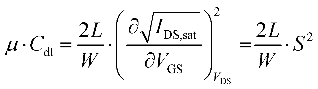
From the equation of standard MOSFETs, the product Cdl·μ can be extracted in the saturation regime as follows:
Gauge factors were calculated employing eqn (3). Both tensile and compressive strains from 0.05% to 0.8% were applied for both OSCs. The manual adjustment of the radius of curvature during real-time monitoring made it impossible to achieve a perfectly linear increase in curvature. Likewise, there is a slight variation between the compression strains applied to the two semiconductors. Finally, the device was returned to the flat position, and a transfer was recorded to assess the recovery of its performance.
Bending measurement setup
For carrying out the bending measurements, a homemade apparatus was conceived by assembling different components (Fig. S2, ESI†). The substrate was fixed by its extremities into a holder. The holder incorporates a pusher block which can be leaned forward by a pivot, connected to a spring. The movement of the pusher block promotes the bending of the substrate in the upward or downward direction. To facilitate and control achieving the different strains (calculated by eqn (2)), different polymethylmethacrylate (PMMA) pieces with known radii were used to force the bending of the substrate at specific radius in tensile strains.3. Results and discussion
Blends of the OSCs diF-TES-ADT with PS of molecular weight of 10 KDa and blends of C8O-BTBT-OC8 with PS of 100 KDa were selected because of their excellent performance in conventional OFET configuration (Fig. 1a).13,37,41 As previously mentioned, diF-TES-ADT:PS films have also shown to exhibit a high performance in EGOFETs.10 Both OSCs were deposited using the BAMS technique on top of pre-patterned S and D electrodes on flexible Kapton substrates, which also contained a lateral G contact (see Experimental section).13,38 As can be observed in the cross-polarised optical microscope images of Fig. 1b and c, highly crystalline and homogeneous thin films were obtained for both materials (see also Fig. S3 for the X-ray diffractogram, ESI†).37 | ||
| Fig. 1 (a) Molecular structure of diF-TES-ADT, polystyrene, and C8O-BTBT-OC8. Polarized optical microscopy images of (b) diF-TES-ADT:PS, and (c) C8O-BTBT-OC8:PS thin films coated on Kapton substrates. The scale bar of POM images is 50 μm. (d) Schematic representation of the EGOFET device configuration employed. | ||
The as-prepared devices were characterized by recording the transfer and output characteristics employing Milli-Q water as electrolyte (Fig. 1d). Water has proven to be an efficient electrolyte for EGOFETs, offering a milder alternative compared to buffer solution electrolytes that contain more ions that tend to degrade faster these devices.6,10,43 In Fig. 2a, the transfer characteristics of diF-TES-ADT:PS and C8O-BTBT-OC8:PS thin films are shown together with the gate-source current (IGS). In the case of EGOFETs, it is common to report the product of the mobility (μ) and the double-layer capacitance (Cdl) to evaluate the performance of the device. This value can be extracted directly from the slope of the transfer characteristics. A Cdl·μ = 0.11 (±0.02) μS V−1 and 0.13 (±0.05) μS V−1 were estimated for diF-TES-ADT:PS and C8O-BTBT-OC8:PS, respectively, in the linear regime, which is in line with EGOFET devices found in the literature.17 It should be noticed that these values are lower than the ones obtained when SiO2 substrates are used instead of Kapton, which is ascribed to the rougher surface of the flexible substrates that might affect the thin film crystallization and the density of charge traps (Fig. S4, ESI†).16 The Ion/off ratio was found to be around 102–103 for both OSCs. Fig. 2b and Fig. S5 (ESI†) display the output characteristics of diF-TES-ADT:PS and C8O-BTBT-OC8:PS EGOFETs, respectively, showing typical p-type behavior and low hysteresis.
 | ||
| Fig. 2 (a) Transfer characteristics (VDS = −0.1 V) and their corresponding source-gate current (dashed lines) for diF-TES-ADT:PS (black curves) and C8O-BTBT-OC8 (red curves) EGOFETs. (b) Output characteristics (VGS = 0.05, 0, −0.1, −0.2, −0.4 V) of diF-TES-ADT:PS EGOFETs. Real-time IDS monitoring of a diF-TES-ADT:PS EGOFET (c) and C8O-BTBT-OC8:PS EGOFET (d) fixing VDS = VGS = −0.2 V. | ||
Electrical stability is still an issue for organic transistors, especially for liquid-gated transistors in which the OSC is in direct contact with the aqueous electrolyte. As previously mentioned, the limited stability in aqueous media restricts the number of OSCs that can be applied in EGOFETs and is surely the main bottleneck that hampers the implementation of these devices for practical applications. In order to gain insights into the stability of our devices in operation, current monitoring tests were performed by continuously applying a source-drain voltage (VDS) and source-gate voltage (VGS) of −0.2 V, whilst recording the source-drain current (IDS). As illustrated in Fig. 2c and d, a quite similar overall behavior for both OSCs is found: an initial current increase is observed followed by a decrease. In the diF-TES-ADT:PS EGOFET, IDS increases during the first 2 minutes until a quasi-steady state is reached. From this time onwards, a slow but constant decrease in current is noticed reaching a value close to the initial one after around 9 minutes. This tendency was also demonstrated by Zhang Q et al.10 In Fig. S6a (ESI†), the transfer curves recorded for the as-prepared device and after the application of the bias stress are reported, where a slight shift of the threshold voltage (Vth) towards more negative values and an increase of the hysteresis are noted. This behavior could be ascribed to an increase in surface defects at the OSC/electrolyte interface due to the long exposition of the OSC to water under electrical stress. On the other hand, C8O-BTBT-OC8:PS exhibits a similar behavior but with a faster current decrease (Fig. 2d). After less than two minutes of measurement, the current starts progressively decreasing reaching around 15% of current decrease with respect to the initial current value after 9 minutes of measurement. In the transfer characteristics recorded before and after the current monitoring (Fig. S6b, ESI†) a large shift of the Vth is observed. Thus, C8O-BTBT-OC8:PS suffer more in water environment under operation than the films based on diF-TES-ADT:PS.10,44,45 This difference in stability between the two materials cannot be ascribed to difference in energy levels, since C8O-BTBT-OC8 has a lower-lying highest occupied molecular orbital (HOMO) and, thus, is less prone to oxidation than diF-TES-ADT.37,39 Thus, the origin might come from differences in thin film morphology, such as a less efficient vertical phase separation between the OSC and the PS, a higher level of charge traps or the presence of more defects in the film.19,46 These factors can lead to the penetration of more ions into the OSC films or to an enhanced trapping of majority carriers, which would result in a diminishment of the electrical performance.47,48 Following, the influence of mechanical stress on the device electrical characteristics during operation were explored for both materials.
Flexibility is a key requirement in sensing and/or wearable applications.4 Considerable literature is dedicated to all-flexible OFETs and the mechanism driving the electrical response under mechanical strain.28,49 Surface strain induced on the OFETs active layer can influence the morphology/structure of the OSC films and modify the hopping energy barrier for charge transport and the intermolecular electronic coupling.27,49–52 Typically, this results in an increase or decrease in the mobility of the thin film when the films are compressed or elongated, respectively. However, the effect of strain in liquid-gated transistors has hardly been explored. Thus, we proceed to explore the electrical response of our EGOFETs under bending strain. There are two different directions in which bending can be addressed, (i) on the concave side of the flexible sheet, resulting in a tensile strain, and (ii) on the convex side, resulting in a compressive strain. To quantitatively estimate the applied strain (ε), a simple relation is used:53
 | (1) |
In the case of thin-film devices, where the overall thickness of the active layer is negligible with respect to the one of the substrate (tsub), ε can be obtained by bending the substrate with a certain bending radius (r):
| ε = tsub/2r | (2) |
Hence, by changing the radius of curvature it is possible to apply different strains and evaluate the electric response of the devices under mechanical stress.
A key parameter to analyze the sensitivity of a material under stress is the so-called gauge factor, k, which can be defined as follows:
 | (3) |
The electrical response applying tensile and compressive strains was evaluated in real-time in EGOFETs previously electrically stabilized (see Experimental section). The device current was stabilized by applying a VDS = −0.2 V and VGS = −0.2 V. Then, a strain was induced for 2 minutes until a new steady state was reached. At this point, the device was placed again in the flat position. Compressive and tensile strains from 0.05% to 0.2% and from 0.1% to 0.8% were applied, respectively. Fig. 3a shows the bending response for diF-TES-ADT:PS under tensile stress, while Fig. 3b displays the bending response when compressive strain is applied. Fig. S7 (ESI†) shows the results obtained for C8O-BTBT-OC8:PS EGOFETs. Compressive and tensile strains foster opposite behaviors. When tensile strain is applied, a decrease in the ISD is induced, which is further noticed when larger strains are applied. On the contrary, the application of a compressive strain, leads to an increase in the ISD, which is also proportionally to the strain value applied. In all the cases, after removing the strain and recovering the flat position, the initial current value was achieved. This behavior is coherent with the results observed in other works using conventional OFETs.28,50,52,55,56
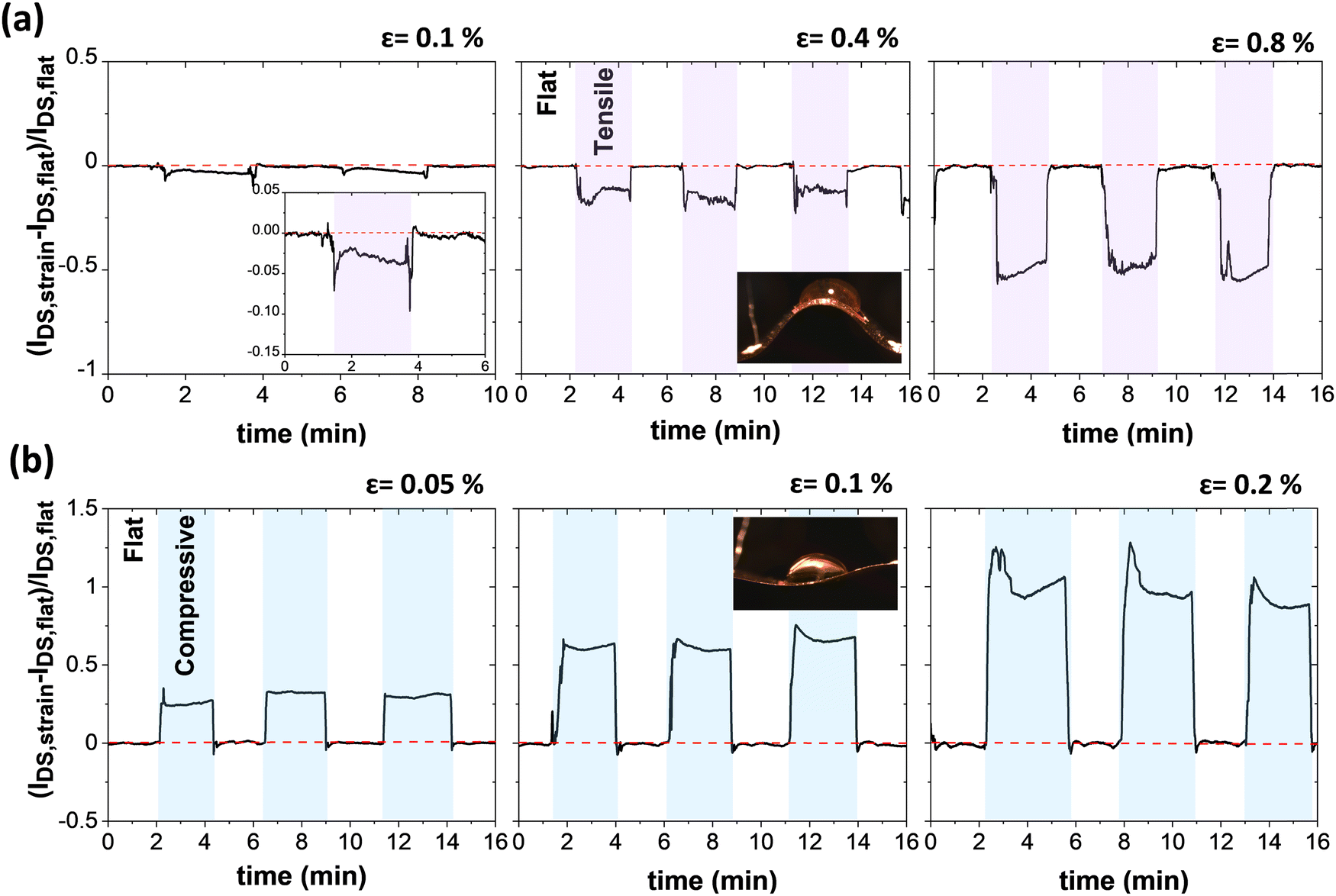 | ||
| Fig. 3 Real-time IDS current monitoring (baseline corrected) of a diF-TES-ADT:PS EGOFET employing Milli-Q water as electrolyte and fixing VDS = −0.2 V and VGS = −0.2 V, applying (a) cyclic tensile strain (purple regions) equal to 0.1, 0.4 and 0.8%, and (b) cyclic compressive strain (blue regions) equal to 0.05, 0.1 and 0.2%. | ||
In order to quantify the results, Fig. 4 plots the average percentage of current difference for each applied strain with respect to the flat position for three different devices. In the same plot the values calculated of their corresponding gauge factors are shown. Both semiconductors exhibit a similar tendency. The maximum gauge factor for tensile stress is found at a strain value of 0.8 for diF-TES-ADT:PS and 0.1 for C8O-BTBT-OC8:PS, giving gauge factors of −17 ± 2 and −58 ± 9, respectively. On the other hand, the maximum gauge factor for compressive stress is found at a strain value of 0.05 for diF-TES-ADT:PS and 0.1 for C8O-BTBT-OC8:PS, giving gauge factor of 429 ± 90 and 210 ± 32, respectively. Noticeably, these values, especially the ones related to compression, are higher than the values typically reported for conventional thin film OFETs with solid dielectric, and they are of the same order of the values reported for single crystals.57–60
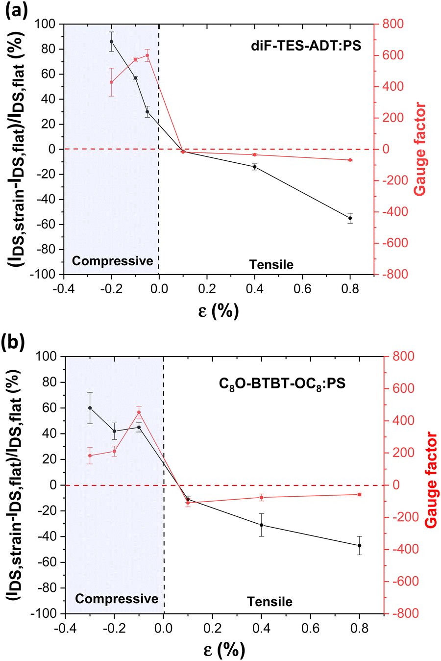 | ||
| Fig. 4 Changes in current (black line) and gauge factor (red line) while applying compressive and tensile strain for (a) diF-TES-ADT:PS and (b) C8O-BTBT-OC8:PS EGOFET employing Milli-Q water as electrolyte in real-time current monitoring. The error bars correspond to the average and standard deviation of at least three different cycles for each applied strain value. | ||
In OFETs, typically the current increase or decrease observed when a compression or tensile stress is applied, respectively, is attributed to changes in the thin film morphology or in the OSC crystal structure.25,61 Here, a similar effect might be playing a key role in the strain response observed in the EGOFETs. However, the high values of the estimated gauge factors seem to point that other mechanisms might also be involved.
As previously mentioned, solid electrolyte OECTs have been widely studied, including their electrical behaviour under mechanical deformation. For instance, an OECT based on PEDOT:PSS and a solid polymer electrolyte was reported to exhibit an exceptional high pressure sensitivity, about 10 times better than OFET-type sensors, at very low voltage (<1 V). This was ascribed to the fact that pressure adjusted the ion injection into the polymer semiconductor.33 In EGOFETs, ions are not expected to be injected into the OSC. However, EGOFETs are highly sensitive to changes occurring at the electrical double layers (EDLs) formed at both the electrolyte/OSC and electrolyte/gate interfaces. Hence, the movement of ions with the applied deformation could also affect these EDLs.
In addition, it was reported that a hydrogel-gated OFET operated as pressure sensor at low pressures (in the range of several hundred Pa to 9 kPa).62 This device response was ascribed to changes in the water dipole orientation within the OSC film induced by the applied pressure. In fact, several works have pointed out that the water orientation can be modulated by an electric field of by pressue.63–65 Further, in a recent publication Ota et al. also reported a pressure sensor based on an ion gel-gated transistor. This was rationalised by the fact that quantity of ions at the EDLs was modified with pressure, which was demonstrated measuring the capacitance of the ion gel sandwiched between two electrodes, and was further corroborated by performing theoretical calculations.66 Another recent work based on EGOFETs using hydrogels or ion gels also showed that the application of tensile stress led to changes in the electrical characteristics, which were dependant on the nature of the solid electrolyte.67 Remarkably, higher electrical changes were observed when using hydrogels as electrolyte, which show higher ionic mobility than ion gels.
Considering all above, we believe that the deformations induced by strain might be also affecting here the EDLs formed at the EGOFET interfaces under the application of an electric field. Further, the high mobility of the ions in the liquid electrolyte might result in a large effect.
In order to gain insights into the sensing mechanism, we also proceed in measuring transfer characteristics of the EGOFETs bended at different radius of curvature, since it is known that variations in the curve slopes could be indicative of alterations in the device capacitance. Unfortunately, the data obtained was not conclusive enough and the changes observed were more attributable to bias stress or to effects caused by the ion diffusion towards the OSC. The same issues were found when performing capacitance measurements of bended devices. We believe that when we do continuous current measurements at fixed gate-source and drain-source voltages, a stable EDL is formed. In these conditions, applying a strain causes a small change in the EDL, which is translated into a change in the measured current. However, when we measure the transfer characteristics, the EDL is continuously changing as a result of the different applied gate voltages, and the small changes occurring at the EDL are no easily detected. Further studies should be conducted for gaining further insights into the mechanisms involved.
This work shows that the application of strain has an influence on the electrical properties of EGOFETs, which should be kept in mind particularly when these devices are applied in flexible sensors. On the other hand, this work also points out that highly strain sensitive devices could be potentially fabricated using EGOFETs based on solid electrolytes.
4. Conclusion
In conclusion, we have studied the electrical performances of two small molecule OSCs, namely diF-TES-ADT and C8O-BTBT-OC8 blended with polystyrene as active materials in EGOFETs. Thin films have been prepared by solution shearing (i.e., BAMS) giving homogeneous films with high crystallinity. Both materials exhibit a high EGOFET performance, although the films based on diF-TES-ADT show a higher stability under continuous water operation.Following, the electrical response of the EGOFETs were studied under the application of tensile and compressive strain. The devices showed a source-drain current increase when compressed and the opposite behavior when a tensile deformation was applied. Remarkably, both EGOFETs exhibited a very high gauge factor, especially when they are compressed. This has been tentatively attributed to be partly due to changes occurring at the electrical double layers. Overall, this work points out the importance of assessing the device performance of EGOFETS when they are mechanically deformed, which is particularly relevant for the development of flexible sensors.
Data availability
The data is available upon request to the authors.Conflicts of interest
There are no conflicts to declare.Acknowledgements
This work was funded by MCIN/AEI/10.13039/501100011033/ERDF, UE with project SENSATION PID2022-141393OB-I00, and through the “Severo Ochoa” Programme for Centers of Excellence in R&D (CEX2023-001263-S) and the Generalitat de Catalunya (2021-SGR-00443). This work was also funded by European Union's Horizon 2020 research and innovation programme under the Marie Skłodowska-Curie grant agreement No 811284 (UHMob). S. R.-M. is enrolled in the UAB Chemistry PhD program. C. M. acknowledges her Juan de la Cierva fellowship. T. S. thanks the Programma per Giovani Ricercatori “Rita Levi Montalcini” year 2020 (grant PGR20QN52R) of the Italian Ministry of University and Research (MUR) for the financial support. Project funded under the National Recovery and Resilience Plan (NRRP), Mission 04 Component 2 Investment 1.5—NextGenerationEU, call for tender no. 3277 dated 30/12/2021 (award number: 0001052 dated 23/06/2022). Y. G. thanks the Belgian National Fund for Scientific Research (FNRS) for financial support through research projects: PDR T.0058.14, Pi-Fast PDR T.0072.18, PICHIR PDR T.0094.22, DIFFRA GEQ U.G001.19, POLYP EQP U.N032.21F, POLYP2 EQP U.N03323F, CHIRI CDR J. 0088.24. G. S. thanks the FNRS for financial support through research project COHERENCE2 No F.4536.23. G. S. is a FNRS Research Associate. G. S. acknowledges financial support from the Francqui Foundation (Francqui Start-Up Grant) and Wiener-Anspach Foundation (FWA, ZT1 research project).References
- Rosaria Anna Picca, Kyriaki Manoli, Eleonora Macchia, Lucia Sarcina, Cinzia Di Franco, Nicola Cioffi, Davide Blasi, Ronald Österbacka, Fabrizio Torricelli, Gaetano Scamarcio and Luisa Torsi, Adv. Funct. Mater., 2019, 30, 1904513 CrossRef.
- Yoeri Van De Burgt, Armantas Melianas, Scott Tom Keene, George Malliaras and Alberto Salleo, Nat. Electron., 2018, 1, 386–397 CrossRef.
- Dion Khodagholy, Thomas Doublet, Pascale Quilichini, Moshe Gurfinkel, Pierre Leleux, Antoinde Ghestem, Esma Ismailova, Thierry Hervé, S. ébastien Sanaur, Christophe Bernard and George G. Malliaras, Nat. Commun., 2013, 4, 1575 CrossRef PubMed.
- Wei Gao, Hiroki Ota, Daisuke Kiriya, Kuniharu Takei and Ali Javey, Acc. Chem. Res., 2019, 52, 523–533 CrossRef CAS PubMed.
- Jonathan Rivnay, Pierre Leleux, Michele Sessolo, Dion Khodagholy, Thierry Hervé, Michel Fiocchi and George G. Malliaras., Adv. Mater., 2013, 25, 7010 CrossRef CAS PubMed.
- Loig Kergoat, Lars Herlogsson, Daniele Braga, Benoit Piro, Minh-Chau Pham, Xavier Crispin, Magnus Berggren and Gilles Horowitz, Adv. Mater., 2010, 18, 2565–2569 CrossRef PubMed.
- Najmeh Delavari, Klas Tybrandt, Magnus Berggren, Benoît Piro, Vincent Noël, Giorgio Mattana and Igor Zozoulenko, J. Phys. D: Appl. Phys., 2021, 54, 415101 CrossRef CAS.
- Rosaria Anna Picca, Kyriaki Manoli, Eleonora Macchia, Angelo Tricase, Cinzia Di Franco, Gaetano Scamarcio, Nicola Cioffi and Luisa Torsi, Front. Chem., 2019, 7, 667 CrossRef PubMed.
- Fabrizio Torricelli, Demetra Z. Adrahtas, Zhenan Bao, Magnus Berggren, Fabio Biscarini, Annalisa Bonfiglio, Carlo A. Bortolotti, C. Daniel Frisbie, Eleonora Macchia, George G. Malliaras, Iain McCulloch, Maximilian Moser, Thuc-Quyen Nguyen, R. óisín M. Owens, Alberto Salleo, Andrea Spanu and Luisa Torsi, Nat. Rev. Methods Primers, 2021, 1, 66 CrossRef CAS PubMed.
- Qiaoming Zhang, Francesca Leonardi, Stefano Casalini, Inés Temiño and Marta Mas-Torrent, Sci. Rep., 2016, 6, 39623 CrossRef CAS PubMed.
- Matteo Parmeggiani, Alessio Verna, Alberto Ballesio, Matteo Cocuzza, Erik Piatti, Vittorio Fra, Candido Fabrizio Pirri and Simone Luigi Marasso, Sensors, 2019, 19, 4497 CrossRef CAS PubMed.
- Sergi Galindo, Adrián Tamayo, Francesca Leonardi and Marta Mas-Torrent, Adv. Funct. Mater., 2017, 27, 1700526 CrossRef.
- Inés Temiño, Freddy G. Del Pozo, M. R. Ajayakumar, Sergi Galindo, Joaquim Puigdollers and Marta Mas-Torrent, Adv. Mater. Technol., 2016, 1, 1600090 CrossRef.
- Oana D. Jurchescu, Sankar Subramanian, R. Joseph Kline, Steven D. Hudson, John E. Anthony, Thomas N. Jackson and David J. Gundlach, Chem. Mater., 2008, 21, 20 Search PubMed.
- Pengshan Xie, Tianjiao Liu, Jia Sun and Junliang Yang, Adv. Funct. Mater., 2022, 32, 2200843 CrossRef CAS.
- Polina A. Shaposhnik, Elena Y. Poimanova, Anton A. Abramov, Askold A. Trul, Daniil S. Anisimov, Elena A. Kretova, Elena V. Agina and Sergey A. Ponomarenko, Chemosensors, 2023, 11, 74 CrossRef CAS.
- Michele Di Lauro, Marcello Berto, Martina Giordani, Simone Benaglia, Guillaume Schweicher, Dominique Vuillaume, Carlo Augusto Bortolotti, Yves Henri Geerts and Fabio Biscarini, Adv. Electron. Mater., 2017, 3, 9 Search PubMed.
- Elena Yu Poimanova, Polina A. Shaposhnik, Daniil S. Anisimov, Elena G. Zavyalova, Askold A. Trul, Maxim S. Skorotetcky, Oleg V. Borshchev, Dmitry Z. Vinnitskiy, Marina S. Polinskaya, Vadim B. Krylov, Nikolay E. Nifantiev, Elena V. Agina and Sergey A. Ponomarenko, ACS Appl. Mater. Interfaces, 2022, 14, 16462–16476 CrossRef CAS PubMed.
- Antonio Campos, Sergi Riera-Galindo, Joaquim Puigdollers and Marta Mas-Torrent, ACS Appl. Mater. Interfaces, 2018, 10, 15952–15961 CrossRef CAS PubMed.
- Francesca Leonardi, Stefano Casalini, Qiaoming Zhang, Sergi Galindo, Diego Gutiérrez and Marta Mas-Torrent, Adv. Mater., 2016, 28, 10311–10316 CrossRef CAS PubMed.
- Gregor Schwartz, Benjamin C.-K. Tee, Jianguo Mei, Anthony L. Appleton, Do Hwan Kim, Huiliang Wang and Zhenan Bao, Nat. Commun., 2013, 4, 1859 CrossRef PubMed.
- Nanshu Lu and Dae-Hyeong Kim, Soft Robot., 2014, 1, 53–62 CrossRef.
- Isacco Gualandi, Marco Marzocchi, Andrea Achili, D. Cavedale, Annalisa Bonfiglio and Beatrice Fraboni, Sci. Rep., 2016, 6, 33637 CrossRef CAS PubMed.
- Giorgio Mattana, Piero Cosseddu, Beatrice Fraboni, George G. Malliaras, Juan P. Hinestroza and Annalisa Bonfiglio, Org. Electron., 2011, 12, 2033–2039 CrossRef CAS.
- Stefano Lai, Inés Temiño, Tobias Cramer, Freddy G. del Pozo, Beatrice Fraboni, Piero Cosseddu, Annalisa Bonfiglio and Marta Mas-Torrent, Adv. Electron. Mater., 2018, 4, 1700271 CrossRef.
- Kenjiro Fukuda, Kenta Hikichi, Tomohito Sekine, Yasunori Takeda, Tsukuru Minamiki, Daisuke Kumaki and Shizuo Tokito, Sci. Rep., 2013, 3, 2048 CrossRef PubMed.
- Piero Cosseddu, Silvia Milita and Annalisa Bonfiglio, IEEE Electron Device Lett., 2012, 33, 113–115 CAS.
- Hyun Ho Choi, Hee Take Yi, Junto Tsurumi, Jae Joon Kim, Alejandro L. Briseno, Shun Watanabe, Jun Takeya, Kilwon Cho and Vitaly Podzorov, Adv. Sci., 2020, 7, 1901824 CrossRef PubMed.
- Jiajun Song, Hong Liu, Zeyu Zhao, Peng Lin and Feng Yan, Adv. Mater., 2024, 36, 2300034 CrossRef CAS PubMed.
- Zeyu Zhao, Zhiyuan Tian and Feng Yan, Cell Rep. Phys. Sci., 2023, 4, 101673 CrossRef CAS.
- Shiming Zhang, Yang Li, Gaia Tomasello, Maddy Anthonisen, Xinda Li, Marco Mazzeo, Armando Genco, P. Grutter and Fabio Cicoira, Adv. Electron. Mater., 2019, 5, 1900191 CrossRef.
- Jianhua Chen, Wei Huang, Ding Zheng, Zhaoqian Xie, Xinming Zhuang, Dan Zhao, Yao Chen, Ning Su, Hongming Chen, Robert M. Pankow, Zhan Gao, Junsheng Yu, Xugang Guo, Yuhua Cheng, Joseph Strzalka, Xinge Yu, Tobin J. Marks and Antonio Facchetti, Nat. Mater., 2022, 21, 564–571 CrossRef CAS PubMed.
- Shuai Chen, Abhijith Suredran, Xihu Wu and Wei Lin Leong, Adv. Funct. Mater., 2020, 30, 2006186 CrossRef CAS.
- Xinyu Tian, Dingyao Liu, Jing Bai, Kai San Chan, Long Ching Ip, Paddy K. L. Chan and Shiming Zhang, Anal. Chem., 2022, 94, 6156–6162 CrossRef CAS PubMed.
- Xihu Wu, Abhijith Surendran, Jieun Ko, Oliver Filonik, Eva M. Herzig, Peter Müller-Buschbaum and Wei Lin Leong, Adv. Mater., 2018, 31, 180554 Search PubMed.
- Yang Li, Shiming Zhang, Xinda Li, Ventaka Ramana Nitin Unnava and Fabio Cicoira, Flexible Printed Electron., 2019, 4, 044004 CrossRef CAS.
- Tommaso Salzillo, Antonio Campos, Adara Babuji, Raul Santiago, Stefan T. Bromley, Carmen Ocal, Esther Barrena, R. émy Jouclas, Christian Ruzié, Guillaume Schweicher, Yves Henri Geerts and Marta Mas-Torrent, Adv. Funct. Mater., 2020, 30, 2006115 CrossRef CAS.
- Freddy G. del Pozo, Simone Fabiano, Raphael Pfattner, Stamatis Georgakopoulos, Sergi Galindo, Xianjie Liu, Slawomir Braun, Mats Fahlman, Jaume Veciana, Concepció Rovira, Xavier Crispin, Magnus Berggren and Marta Mas-Torrent, Adv. Funct. Mater., 2015, 26, 2379–2386 CrossRef.
- Christian Ruzié, Jolanta Karpinska, Anne Laurent, Lionel Sanguinet, Simon Hunter, Thomas D. Anthopoulos, Vincent Lemaur, J. érôme Cornil, Alan R. Kennedy, Oliver Fenwick, Paolo Samorì, Guillaume Schweicher, Basab Chattopadhyay and Yves Henri Geerts, J. Mater. Chem. C, 2016, 4, 4863–4879 RSC.
- Jeremy w Ward, Marsha A. Loth, R. Joseph Kline, Mariona Coll, Carmen Ocal, John E. Anthony and Oana D. Jurchescu, J. Mater. Chem., 2012, 22, 19047–19053 RSC.
- Tommaso Salzillo, Nieves Montes, Raphael Pfattner and Marta Mas-Torrent, J. Mater. Chem. C, 2020, 8, 15361–15367 RSC.
- Tommaso Salzillo, Francesco D’Amico, Nieves Montes, Raphael Pfattner and Marta Mas-Torrent, CrystEngComm, 2021, 23, 1043–1051 RSC.
- Wei Huang, Jianhua Chen, Gang Wang, Yao Yao, Xinming Zhuang, Robert M. Pankow, Yuhua Cheng, Tobin J. Marks and Antonio Facchetti, J. Mater. Chem. C, 2021, 9, 9348–9376 RSC.
- Nicolò Lago, Marco Buonomo, Sara Ruiz-Molina, Andrea Pollesel, Rafael Cintra Hensel, Francesco Sedona, Mauro Sambi, Marta Mas-Torrent, Stefano Casalini and Andrea Cester, Org. Electron., 2022, 106, 106531 CrossRef CAS.
- Xingyu Jiang, Cheng Shi, Zi Wang, Lizhen Huang and Lifeng Chi, Adv. Mater., 2023, 36, 2308952 CrossRef PubMed.
- Adrian Tamayo, Ilaria Fratelli, Andrea Ciavatti, Carme Martínez-Domingo, Paolo Branchini, Elisabetta Colantoni, Luca Tortora, Adriano Contillo, Raul Santiago, Stefan T. Bromley, Beatrice Fraboni, Marta Mas-Torrent and Laura Basiricò, Adv. Electron. Mater., 2022, 8, 2200293 CrossRef CAS.
- Shubham Tanwar, Ruben Millan-Solsona, Sara Ruiz-Molina, Marta Mas-Torrent, Adrica Kyndiah and Gabriel Gomila, Adv. Mater., 2024, 36, 2309767 CrossRef CAS PubMed.
- Hamna F. Haneef, Adrew M. Zeidell and Oana D. Jurchescu, J. Mater. Chem. C, 2020, 8, 759–787 RSC.
- Piero Cosseddu, Gianmarco Tiddia, Silvia Milita and Annalisa Bonfiglio, Org. Electron., 2013, 14, 206–211 CrossRef CAS.
- Tsuyoshi Sekitani, Yusaku Kato, Shingo Iba, Hiroshi Shinaoka, Takao Someya, Takayasu Sakurai and Shinichi Takagi, Appl. Phys. Lett., 2005, 86, 073511 CrossRef.
- Tsuyoshi Sekitani, Shingo Iba, Yusaku Kato and Takao Someya, Jpn. J. Appl. Phys., 2005, 44, 2841–2843 CrossRef CAS.
- V. Scenev, Piero Cosseddu, Annalisa Bonfiglio, Ingo Salzmann, N. Severin, Martin Oehzelt, Norbert Koch and J. ürgen P. Rabe, Org. Electron., 2013, 14, 1323–1329 CrossRef CAS.
- Jay Lewis, Mater. Today, 2006, 9, 38–45 CrossRef CAS.
- Zhiyuan Liu, Dianpeng Qi, Peizhi Guo, Yan Liu, Bowen Zhu, Hui Yang, Yaquing Liu, Bin Li, Chenguang Zhang, Jiancan Yu, Bo Liedberg and Xiaodong Chen, Adv. Mater., 2015, 27, 6230–6237 CrossRef CAS PubMed.
- Anatoliy N. Sokolov, Yadong Cao, Olasupo B. Johnson and Zhenan Bao, Adv. Funct. Mater., 2012, 22, 175–183 CrossRef CAS.
- Haiting Wang, Liangliang Deng, Q. Tang, Y. Tong and Yichun Liu, IEEE Electron Device Lett., 2017, 38, 1598–1601 CAS.
- Haiting Wang, Yanhong Tong, Xiaoli Zhao, Qingxin Tang and Yichun Liu, Org. Electron., 2018, 61, 304–311 CrossRef CAS.
- A. L. Briseno, Ricky J. Tseng, M. M. Ling, E. H. L. Falcao, Yang Yang, F. Wudl and Zhenan Bao, Adv. Mater., 2006, 18, 2320–2324 CrossRef CAS.
- Takayoshi Kubo, Roger Häusermann, Junto Tsumuri, Junshi Soeda, Yugo Okada, Yu Yamashita, Norihisa Akamatsu, Atsushi Shishido, Chikahiko Mitsui, Toshihiro Okamoto, Susumu Yanagisawa, Hiroyuki Matsui and Jun Takeya, Nat. Commun., 2016, 7, 11156 CrossRef CAS PubMed.
- Qingxin Tang, Yanhong Tong, Yongmei Zheng, Yudong He, Yajie Zhang, Huanli Dong, Wenping Hu, Tue Hassenkam and Thomas Bjornholm, Small, 2011, 7, 189–193 CrossRef CAS PubMed.
- Damien Thuau, Katherine Begley, Rishat Dilmurat, Abduleziz Ablat, Guillaume Wantz, C. édric Ayela and Mamatimin Abbas, Materials, 2020, 13, 1583 CrossRef CAS PubMed.
- Qiaoming Zhang, Francesca Leonardi, Raphael Pfattner and Marta Mas-Torrent, Adv. Mater. Interfaces, 2019, 6, 1900719 Search PubMed.
- Gaurav Chopra and Michael Levitt, Proc. Natl. Acad. Sci. U. S. A., 2011, 108, 14455–14460 Search PubMed.
- Yuchi He, Gang Sun, Kenichiro Koga and Limei Xu, Sci. Rep., 2014, 4, 6596 CrossRef CAS PubMed.
- Belisa R. H. de Aquino, H. Ghorbanfekr-Kalashami, M. Neek-Amal and F. M. Peeters, Phys. Rev. B, 2018, 97, 144111 Search PubMed.
- Kota Inoue, Kazumoto Miwa, Sunao Shimizu, Kazuhide Ueno, Junichiro Ohe and Shimpei Ono, Kiroki Ota. IEEE 37TH International Conference on Micro Electro Mechanical Systems (MEMS), 2024, 604–605.
- Mona Azimi, Arunprabaharan Subramanian, Jiaxin Fan, Francesca Soavi and Fabio Cicoira, J. Mater. Chem. C, 2023, 11, 4623 RSC.
Footnotes |
| † Electronic supplementary information (ESI) available. See DOI: https://doi.org/10.1039/d4tc05403b |
| ‡ Equally contributed. |
| § Current address: Department of Industrial Chemistry “Toso Montanari”, University of Bologna, Via Gobetti 85, 40129 Bologna, Italy. |
| This journal is © The Royal Society of Chemistry 2025 |