
 Open Access Article
 This Open Access Article is licensed under a Creative Commons Attribution-Non Commercial 3.0 Unported Licence
Amphoteric doping and thermoelectric transport in the CuInTe2–ZnTe solid solution†
Vanessa
Meschke‡
 a,
Angela
Pak‡
b,
Jesse M.
Adamczyk
a,
Lìdia C.
Gomes
b,
Samantha
Baumann
a,
Grace
Rome
a,
Claire
Porter
a,
Kamil
Ciesielski
a,
Elif
Ertekin
b and
Eric
Toberer
*a
a,
Angela
Pak‡
b,
Jesse M.
Adamczyk
a,
Lìdia C.
Gomes
b,
Samantha
Baumann
a,
Grace
Rome
a,
Claire
Porter
a,
Kamil
Ciesielski
a,
Elif
Ertekin
b and
Eric
Toberer
*a
aColorado School of Mines, 1500 Illinois St., Golden, CO, USA. E-mail: etoberer@mines.edu
bUniversity of Illinois Urbana-Champaign, Champaign, IL, USA
First published on 26th March 2025
Abstract
The chalcopyrite CuInTe2 is a promising thermoelectric material; here, optimal carrier concentrations can be achieved through careful stoichiometric control or the introduction of extrinsic dopants such as Zn. However, CuInTe2 is challenging to rationally dope: Zn can expected to substitute on either cation site, and there are a large number of competing low energy native defects. Zn doping is further complicated by the complete solid solution formed between CuInTe2 and ZnTe, which creates uncertainty in the experimental elemental chemical potentials. In this work, first principles calculations are united with experimental synthesis and transport measurements to predict the formation energies of defects in Zn-doped CuInTe2. This is a challenging task: within Zn-doped CuInTe2, we face an expansive four-dimensional single phase region in chemical potential space. To render this space tractable, we present how native and extrinsic defects evolve when: (i) varying Cu, In, and Te chemical potentials for fixed Zn chemical potential, and (ii) adjusting Zn chemical potential for fixed Cu, In, and Te chemical potential. Computationally, we predict that the introduction of Zn significantly alters the native defect landscape, generates large concentrations of ZnCu–ZnIn defect complexes, and serves as an ambipolar dopant. These predictions are supported by electronic transport measurements on bulk, polycrystalline samples that further demonstrate the broad range of charge carrier concentrations achievable in the space. These results come together in a unified workflow to account for the interplay between native defects, ambipolar extrinsic dopants, and solid solution behavior in Zn-doped CuInTe2.
1 Introduction
Diamond-like semiconductors (DLS) are a chemically diverse class of materials that have long been used in microelectronic, thermoelectric, and optoelectronic applications.1–6 This wide range of applications stems from ability of the DLS space to accommodate a wide swatch of chemistries, ranging from elemental Si to quarternary compounds such as Cu2HgGeTe4.7,8 Throughout the mutation from elemental Si to the quarternary compounds, charge neutrality is maintained by balancing either numerous cations or anions (i.e. I–III–VI2 ternaries). The chemical diversity of the DLS space results in materials whose properties range from electrically insulating to metallic, prompting the need to optimize the carrier concentration through the introduction of extrinsic dopants.9,10For these chemically complex spaces, doping is a difficult task that requires optimizing over a highly dimensional space of chemical potential, synthesis conditions, dopant selection, etc. For the I–III–VI2 DLS space, the doping process is further complicated the ability for II2+ dopants (i.e. Zn, Cd, and Hg) to occupy both the I1+ and III3+ sites, resulting in uncertain doping conditions, the formation of competing defects, and the possibility for mixed oxidation states of the host. Additionally, many of these cationic dopants are known to form solid solutions with the host I–III–VI2 compound, creating a wide range of achievable dopant concentrations and obfuscating the chemical potential space. Fortunately, the combination of first principles defect energetic calculations and smart experimental campaigns drastically reduces the need to rely on chemical intuition or employ guess-and-check methods.11,12 However, the ability for the dopants to form solid solutions with the host has not been largely considered in these methods, and dopants are typically treated in a dilute, non-interacting limit. In this work, we demonstrate a treatment of this solid solution, non-dilute behavior in Zn-doped thermoelectric material CuInTe2.
CuInTe2 has shown promise as a thermoelectric material since 2012 when thermoelectric figure of merit zT > 1 was first identified13 despite a high lattice thermal conductivity (∼5.5 W m−1 K−1 at 300 K).13–15 However, numerous studies have found that synthesizing the compound in a copper-deficient regime improves the thermoelectric performance by increasing the carrier concentration and reducing the lattice thermal conductivity.16–18 From our previous work, we have shown that synthesizing in a copper-deficient regime increases the copper vacancy concentration, accounting for the improvement in the p-type thermoelectric performance.14 Although CuInTe2's thermoelectric performance has been successfully improved through native defect engineering, extrinsic doping strategies have also been explored.
To date, many extrinsic doping studies in CuInTe2 have focused on tuning p-type performance in an indium-deficient regime.16,19–22 These studies typically employ a “substitutional” strategy, whereby some fraction of In3+ is removed from the nominal stoichiometry and “substituted” for a 2+ dopant (i.e., Zn, Cd, and Hg). The compositional schemes are represented as CuIn1−xDxTe2, where the dopant atom, D, is assumed to sit on the In site based on chemical intuition. This assumption poses an inherent problem: 2+ dopants may act aliovalently in the CuInTe2 space, able to occupy either the Cu1+ or the In3+ site, and dopant site preference may not be determined through synthesizing with the intuitive elemental deficiency.
Further complicating the analysis of 2+ dopant energetics in the DLS space is their proclivity to form chalcogenide-based zinc blende materials, which are well known to form full solid solutions with other diamond-like structures.23,24 Given the crystal structures of CuInTe2 and ZnTe, shown in Fig. 1, this is rather expected: the chalcopyrite structure of CuInTe2 (left) is nearly identical to two cubic zinc blende cells stacked upon one another (right). As a result of this solid solution behavior, increasing the Zn concentration will never result in Zn or ZnTe precipitation, and the Zn chemical potential may take any value from -inf (no Zn incorporated) to 0 eV (fully incorporated). Experimentally, this eliminates the use of phase boundary mapping to pin the chemical potentials,25,26 and computationally creates a complex, 4D space through which the chemical potential must be optimized, a fact that has largely been neglected in previous studies.19–22
 | ||
| Fig. 1 The chalcopyrite-structured CuInTe2 (left) forms a solid solution with zinc blende structured ZnTe (right). A single unit cell of ZnTe is shown with darkened boundaries. | ||
The ambipolar, solid solution behavior of Zn in CuInTe2 is not unique; such behavior has also been explored for the alloy between CuInSe2 and ZnSe to reduce reliance on In while maintaining single phase purity for photovoltaic applications.27,28 However, the complexity of the solid solution combined with the aliovalent dopant behavior has limited studies on the efficacy of Zn-doped CuInSe2 as a solar cell material.29,30 In increasing complexity, ZnSnN1−x–ZnO2x has been studied for solar applications, where the mixed oxidation on both the cation and anion sublattices has been leveraged to tune materials properties. Again, though, the dual site disorder creates a complex chemical potential space with large impacts on the carrier concentration and solar cell performance depending on the local coordination environment.31,32 Such examples highlight how control of the chemical potentials of all the elements are crucial in doping within solid solutions of dopants and their hosts. Further, it demonstrates the need for consideration of the intersection of ambipolar dopants and phase boundary mapping in complex materials; the complexity in the interplay of native defects and an ambipolar dopants is non-trivial.
In this work, we assemble a framework to account for the interplay between native defects, ambipolar extrinsic dopants, and solid solution behavior in Zn-doped CuInTe2. First principles calculations of the defect formation energies as a function of the dopant chemical potential are paired with the characterization of bulk, polycrystalline samples of natively and Zn-doped CuInTe2. An iterative process considering the experimentally measured and theoretically predicted carrier concentration allows for tuning the dopant chemical potential to reasonable dopant levels. The union of native and dopant defect calculations with experimental measurements ultimately provides insight into the native and extrinsic defects in CuInTe2 and the affiliated electronic properties.
2 Methods
2.1 First principles calculations
Total energies of bulk and defect-containing supercells were calculated using density functional theory (DFT),33,34 as implemented in the Vienna ab initio simulation package (VASP).35 The projector augmented wave (PAW) method36 was used to treat the core and valence electrons. The Heyd–Scuseria–Ernzerhof (HSE06)37 hybrid functional was used as the exchange–correlation term. Despite their higher computational cost, hybrid functionals typically show improved accuracy in computed formation energies, band gaps, and other quantities important for accurate defect calculations.The total energy and total force for structural relaxations were converged to 10−4 eV and 0.01 eV Å−1 respectively. The total energy and total force convergence criteria for defect calculations were 10−4 eV and 0.03 eV Å−1 respectively. The Kohn–Sham orbitals were expanded using a plane-wave basis with a cutoff energy of 400 eV. For the bulk unit cells, the Brillouin zone was sampled using a Γ-centered 4 × 4 × 4 Monkhorst–Pack k-point grid.38 The bulk density of states was taken from a 10 × 10 × 10 Monkhorst–Pack k-point grid to reach a density of 8000 per atom k-point density. Supercells of dimensions 2 × 2 × 2, resulting in 64 atoms, were used for the defect calculations. In this case, a Γ-centered 2 × 2 × 2 k-point mesh was employed. Due to the presence of heavy Te atoms, spin–orbit coupling effects are accounted for by applying shifts to band edge positions used to obtain defect diagrams.
2.2 Phase stability and defect formation energies
A critical step in calculating defect formation energies is determining the bounds of the elemental chemical potentials that define the range of the compound's stability. The chemical potential describes the energy required to exchange an atom with its infinite reservoir and is the key property relating the realm of defect calculations with experimental conditions. The bounding points in chemical potential space can be directly correlated to regions of composition space; for a ternary system, these points correspond to three phase regions.25,26 For CuInTe2, first principles calculations predict six invariant points where CuInTe2 forms three phase equilibria with competing compounds. These points are labeled CI1, CI2, …, CT2 and are shown in the 3-dimensional chemical potential space map in Fig. 2 as the intersection points of the CuInTe2 plane (grey) with two other compounds' planes. The notation for each invariant point was selected to denote which two elements (C: Cu, I: In, T: Te) are in excess at the point. For the point CI2′, the prime notation was used due to the proximity of this equilibrium point to point CI2. In this work, the phase stability of CuInTe2 differs slightly from our previous work due to our incorporation of the ordered vacancy compound CuIn5Te8, which also changes our presented defect energetics slightly.14 | ||
| Fig. 2 CuInTe2 (grey) lives within the Cu–In–Te elemental chemical potential space. Binary and ternary compounds that are more stable than the constituent elements or competing phases appear as bevels to the cube. There are six invariant points involving CuInTe2; at each invariant point three phases are in equilibrium. The label at each invariant point (black circles) indicates which two elements are in excess (C: Cu, I: In, T: Te). For each element, the Δμ range considered is from 0 to −2 eV per atom. Analysis presented in Fig. 3 will focus on the CT2 and IT1 invariant points. | ||
For a compound in thermodynamic equilibrium, the chemical potential is the sum of the number of atoms of type i in the composition times the chemical potential of species i . For CuInTe2, the chemical potential is written as:
| μCuInTe2 = μCu + μIn + 2μTe | (1) |
| μCuInTe2 = (μ0Cu + ΔμCu) + (μ0In + ΔμIn) + 2(μ0Te + ΔμTe) | (2) |
Defect formation energies ΔHD,q of defects D in charge state q are obtained using the standard supercell approach.39 Formally, ΔHD,q is given by ref. 40:
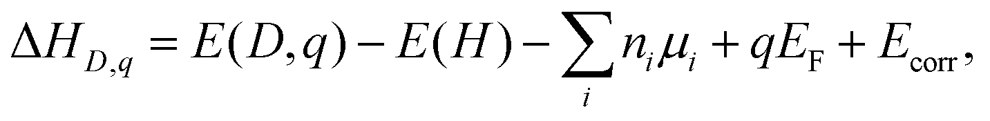 | (3) |
Defect concentration is assessed by computing ΔHD,q for defects in their relevant charge states and multiplying by a site density factor. In this work, we assume that defect concentrations are determined at the synthesis temperature and cannot equilibrate to measurement temperature, whereas electron and hole concentrations can and do equilibrate. Following this assumption, the defect formation energies calculated with eqn (3) can be related to defect concentration by:
 | (4) |
 | (5) |
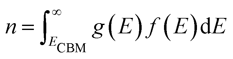 | (6) |
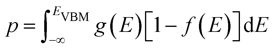 | (7) |
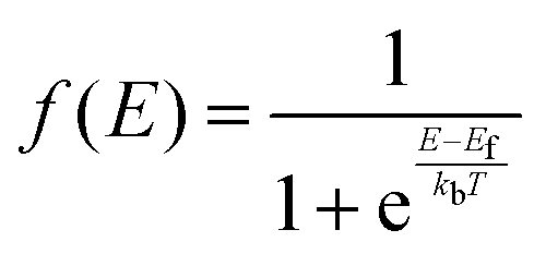 | (8) |
2.3 Experimental synthesis and measurement
High purity Cu granules (99.999%, Alpha Aesar), In shot (99.999%, 5N Plus), Te shot (99.999%, 5N Plus), Zn powder (99.99%, Alfa Aesar), and Cd shot (99.99%, Alfa Aesar) were weighed in batches totaling 5 g of material. Each batch of material was loaded into a clean fused silica ampoule and sealed under vacuum. Ampoules were kept as small as possible to mitigate evaporation of elements. Ampoules were individually placed into a furnace at 1000 °C for 20 minutes with and shaken in 5 minute intervals. Hot ampoules were then removed from the furnace and quenched in cold water to reduce phase separation during solidification. Ingots of solidified material were removed from ampoules, ground into powder with an agate mortar and pestle, and then sieved through a 200 mesh sieve. Approximately 3 g of powder was loaded into graphite foil-lined graphite dies and placed in a vacuum hot press. Samples were pressed at 550 °C for 12 hours under 40 MPa of pressure. The pressure on the die was released, and the die was held at 550 °C for 1 hour as an annealing treatment before cooling to room temperature. Pellets were removed from the graphite dies and hand-polished to a parallelness within ±5 μm using a final grit paper of 2000 grit.High-temperature measurement of the Seebeck coefficient was performed from 323 K to 673 K using a custom-built apparatus.47 All samples underwent a minimum of 2 heating and cooling cycles during measurement to guarantee measurement consistency and ensure samples are not thermally evolving. High temperature resistivity and Hall effect measurements were performed on a custom built apparatus with a Van der Pauw geometry.48 Thermal diffusivity measurements were performed under vacuum using a Netzsch LFA-467 Flash Diffusivity system. Density was determined by the mass and geometry of the samples. Calculation of thermal conductivity was done using the Dulong-Petit approximation. Crystal structures of the samples were assessed through X-ray diffraction (XRD) measurements performed on the powders using a Bruker D2 Phaser (Cu-Kα radiation) in a θ–2θ configuration for 2θ running from 10° to 100°. Patterns were compared to known experimental powder diffraction patterns.49 SEM imaging and EDS were performed using an FEI Quanta 600i SEM. Grain sizes of the samples were determined from 5 images at 5 different locations on each sample. For each phase in a sample, EDS measurements were taken at 5 different locations on the samples with the averaged data shown with the fingerprinted XRD patterns in ESI,† Fig. S1–S4.
3 Results & discussion
We begin by revisiting the native defects and phase stability of CuInTe2. With this baseline, first principles methods are used to predict the energetics of natively- and extrinsically-doped CuInTe2. These predictions are cross-referenced with experimental transport measurements of bulk, Zn-doped CuInTe2 with either Cu or In deficiency. The effects of the dopant are compared to the undoped samples at each point of interest, showcasing the varying behavior of CuInTe2 and the versatility of Zn as an ambipolar dopant.3.1 Phase stability and defects in undoped CuInTe2
Understanding a compound's extent in chemical potential space against other competing phases is critical for predicting defect energetics. In Fig. 2, we show the phase stability across the Cu–In–Te ternary in elemental chemical potent space at 0 K. This space is constructed by first creating three orthogonal planes where the chemical potential of the elements is equal to zero (ΔμCu = 0, ΔμIn = 0, and ΔμTe = 0). The surfaces are constructed from planes whose equations following the format nCuΔμCu + nInΔμIn + nTeΔμTe − ΔH = 0. Additional planes are cut away from the box where compounds are more stable than the elemental solids. Junctions between planes correspond to two (line) and three (point) phase equilibria. The grey point at the origin would correspond to having elemental Cu, In, and Te in equilibrium; the system lowers its energy by moving inwards to form compounds. Further introduction to the chemical potential space is provided in the Methods section. CuInTe2 has six three-phase invariant points in this chemical potential space; these are denoted in terms of which elements have high chemical potential. Overall, the CuInTe2 phase spans a broad range of chemical potentials for each elemental species (Cu: −0.622 to 0 eV per atom; In: −1.414 to −0.143 eV per atom; Te: −0.675 to 0 eV per atom). These broad ranges in chemical potential enable large variations in the defect energetics for the system.The effect of changes in chemical potential on defect and carrier concentrations is summarized in the Brouwer defect diagram (Fig. 3a), which plots the concentrations as one traverses the perimeter of the CuInTe2 chemical potential plane. The energetics underlying the concentrations in the Brouwer diagram are shown in the defect diagrams for two representative points in the space: copper-poor (IT1) and indium-poor (CT2) conditions (Fig. 3b and c, respectively). The defect diagrams of the remaining points are shown in the ESI,† in Fig. S6. As discussed in the methods, defect concentrations are set during synthesis and do not evolve with temperature; as such, the vertical dashed line (EdefF) shows the Fermi level at the time of defect formation. The VCu−1 proves to be the dominant defect in nearly all available chemical potentials. For indium-deficient conditions, CuIn is the dominant defect; at all compositions, InCu is 2+ orders of magnitude lower in concentration. The defect diagrams in Fig. 3b and c also display the dilute defects that are not visible on the Brouwer diagrams; for example, regardless of chemical potential, VIn and VTe are extremely dilute.
 | ||
| Fig. 3 For undoped CuInTe2, the perimeter of the single phase chemical potential region in Fig. 2 is traced to map out the defect and charge carrier concentrations. VCu−1 and CuIn prove to be the two most prevalent defects. Given the absence of compensating native defects, the hole carrier concentration tracks these defect concentrations. (b) and (c) The individual defect diagrams for undoped IT1 and CT2 show the available dopability windows. The 300 K Fermi level positions (Eeq.F) shifts significantly from the 623 K (EdefF) position due to the need to maintain charge neutrality upon quenching. (d) The impact of Zn doping can be traced around the perimeter of the CuInTe2 chemical potential space. Here, the Brouwer band diagram is calculated assuming a constant Zn chemical potential (ΔμZn = −1.25 eV per atom). Three charged defects, ZnIn, ZnCu and VCu, significantly alter the carrier concentration from the undoped case. Additionally, the neutral defect complex, ZnIn–ZnCu lowers the Zn dopant efficiency. (e) In IT1, the optimal ΔμZn value was found to be −1.25 eV per atom, pinning the synthetic Fermi level to nearly identical energies of VCu and ZnCu, resulting in heavy charge compensation. The ZnIn–ZnCu defect complex was calculated to have a negative formation energy (−0.414 eV) at this combination of ΔμZn and synthetic temperature. (f) At point CT2, the optimal ΔμZn was found to be −1.38 eV per atom. Under these conditions, ZnIn proves to be a far higher concentration acceptor defect than native CuIn, leading to higher hole concentrations. | ||
With the defect concentrations established at high temperature, the hole carrier concentrations can then be assessed at lower temperatures. In Fig. 3a, the hole carrier concentration is determined by calculating the charge neutrality condition at the measurement temperature (300 K), as discussed in the Methods. The intrinsic chemistry of CuInTe2 results in persistent p-type behavior due to an excess of Cu vacancies in copper-deficient conditions and CuIn antisite defects in copper-rich conditions, which ultimately pin the Fermi level mid-gap and limit n-type dopability.14
Next, we move to introducing Zn to the system. As CuInTe2 and ZnTe form a full solid solution, the exact chemical potential of Zn during synthesis is elusive. As such, we initially estimate the Zn chemical potential by considering the nominal synthetic stoichiometry; this suggests a ΔμZn between −2 and −1 eV per atom as the bounds for our chemical potential sweeps. By shifting the ΔμZn, the formation energy of the Zn-containing defect also shifts, altering the position of the Fermi level, and ultimately the carrier concentration. The relationship between ΔμZn, synthetic temperature, and carrier concentration are shown for a wide selection of values in Fig. S5 (ESI†). Considering both the undoped and doped experimental results at IT1 and CT2, a universal synthetic temperature of 623 K agreed well with the computational predictions of carrier concentration. Here, synthesis temperature refers to the temperature at which defects are effectively quenched into the sample due to their limited mobility; this temperature is used in eqn (4).
Having established a synthesis temperature, we next estimate the ΔμZn values of the doped samples. In Fig. 4, the impact of ΔμZn on the synthetic Fermi level is shown for the two invariant points (IT1 and CT2) considered experimentally. Based on the resulting carrier concentration that emerges from charge neutrality conditions shown in Fig. S5 (ESI†), we select ΔμZn = −1.38 eV per atom as a suitable value for point CT2 (indium-deficient conditions) and ΔμZn = −1.25 eV per atom for point IT1 (copper-deficient conditions). We emphasize that this analysis is a hybrid approach that unites experiment and theory rather than a validation effort.
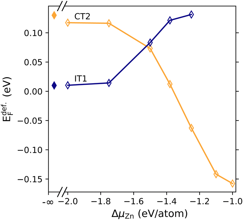 | ||
| Fig. 4 When ΔμZn is varied, the Fermi level shows significant variation compared to the undoped compositions (ΔμZn = −∞). For copper-deficient point IT1, increasing the ΔμZn moves the Fermi level closer to midgap until ΔμZn > −1.25 eV per atom is reached, at which point many of the dopant defects have negative formation energies. In contrast, increasing ΔμZn at indium-deficient point CT2 moves the Fermi level into to the valence band. Here, EdefF. refers to the Fermi level where defect concentrations are equilibrated at a synthesis Tsynth. = 623 K. | ||
Having estimated the chemical potentials of Zn, we consider the impact of Zn holistically on the native and extrinsic defects. In Fig. 3d, the concentrations of defects and carriers are shown for the perimeter of the CuInTe2 chemical potential space for a ΔμZn = −1.25 eV per atom, the value best suited for point IT1. The set of defect diagrams that are used to build Fig. 3d are shown in Fig. S7 (ESI†). The analogous Brouwer diagram for ΔμZn = −1.38 eV per atom is shown in Fig. S8 (ESI†) with the underlying defect diagrams presented in Fig. S9 (ESI†). For the extrinsic Zn dopant, substitution on the cation sites results in three regimes: (i) Cu vacancies remain low energy, though they are matched with ZnCu (CI2, CI2′), (ii) ZnCu is favored over VCu (IT1, CT1), and (iii) ZnIn dominates (CT2, CI1). Similarly, the carrier concentration follows trends with the regimes: in (i), carriers remain low due to relatively high defect energetics and large amounts of compensation, (ii) shows a slight rise but remains low due to some competing defects, and (iii) is high due to the high ZnIn concentrations. Compared to the undoped case, there are either regions where the Zn defects result in increased carrier concentration (CI1, CT1, CT2), or are pushed closer to bipolar behavior with lower carrier concentrations (CI2, CI2′, IT1).
While the ZnCu and ZnIn are calculated using a dilute defect approximation involving supercells, we also consider the formation of defect pairs as the Zn concentration is, experimentally, 2% of the cation sites. We find the neutral defect complex ZnCu–ZnIn to be extremely favorable at this ΔμZn in nearly all synthetic conditions. The only exception is for tellurium-deficient conditions (CI1, CI2, CI2′). Here, the combined ‘cost’ of removing copper and indium drives the defect energy higher. As such, the dopant efficiency of Zn is expected to be significantly compromised due to the formation of neutral defect clusters at high concentration.
Considering the defect diagrams shown in Fig. 3e and f, the impact of Zn doping has wildly different impacts at the different phase equilibria points selected. First, doping point IT1 results in heavily compensated behavior due to the ZnIn and ZnCu defects. The limit of the Zn compensation is set by the intersection of these two defects with the x-axis: EF is pinned at the point where the ΔHD = 0, ultimately limiting the achievable n-type dopability. As such, the Fermi level at measurement (EF) ultimately ends up inside the valence band at room temperature.
3.2 Experimental doping
The carrier concentrations discussed above to set ΔμZn originate from measurements of bulk, single phase polycrystalline pellets, whose SEM images and X-ray diffraction patterns are shown in Fig. S1–S4 (ESI†). The properties of these pellets, and their undoped counterparts, are considered herein. The impact of the changing host elemental chemical potentials on the native and extrinsic defects, defect compensation, and the formation of defect complexes is probed through experimental measurement of the carrier concentration and electrical resistivity. Further, with the variation in defect chemistry, we explore the impact of defects on electronic mobility and lattice thermal conductivity.Across all of chemical potential space, undoped CuInTe2 has been reported to have carrier concentrations spanning 1 × 10¹⁵–3 × 1019 cm−3.14 As shown in Fig. 5a, the focus on indium- and copper-deficient conditions restricts this significantly: the sample synthesized in indium-deficient conditions (CuIn0.96Te2, filled gold circles) has a carrier concentration of 1 × 10¹⁹ h+ cm−3, while the sample prepared in copper-deficient (Cu0.96InTe2, filled blue diamonds) conditions has a slightly increased carrier concentration of 3 × 10¹⁹ h+ cm−3. As discussed above, while the carrier concentrations are similar, the dominant defects are distinct (VCuvs. CuIn). Similar effects are seen in the electrical resistivity measurements shown in Fig. 5b, where the copper-deficient sample (Cu0.96InTe2) is slightly less resistive than the indium-deficient (CuIn0.96Te2).
 | ||
| Fig. 5 (a) The Hall carrier concentration with Zn doping shows evidence of ambipolar doping when compared to analogous undoped compositions. For copper-deficient CuInTe2 (Cu0.96InTe2), the addition of Zn (Cu0.96InTe2Zn0.04) significantly lowers the carrier concentration. The opposite response is found for the indium-deficient samples. (b) The reduction in carrier concentration induced by Zn doping of copper-deficient CuInTe2 is consistent with the massive increase in electrical resistivity. Likewise, Zn doping of indium-deficient CuInTe2 (CuIn0.96Te2Zn0.04) leads to low electrical resistivity. (c) The temperature dependent Seebeck coefficients follow expected trends with respect to carrier concentration. The highly resistive Zn-doped copper-deficient CuInTe2 (Cu0.96InTe2Zn0.04) shows evidence of bipolar transport at all temperatures measured. | ||
As shown in Fig. 5a and b, doping the copper-deficient sample with zinc (Cu0.96InTe2Zn0.04, IT1) results in a drastic reduction of the carrier concentration and a large increase in electrical resistivity. Additionally, the carrier concentration and resistivity show little temperature dependence until ∼450 K, beyond which point the resistivity reduces to ∼104 mW cm due to carrier activation. Given the defect diagrams for the doped and undoped copper-deficient conditions in Fig. 3b and e, respectively, the behavior of the doped sample can understood through the defect energetics. As shown in Fig. 3b, the undoped sample shows a strong preference for VCu1− defects, with little competition from the compensating InCu2+ defect that forms at a significantly higher energy at the synthesis conditions. However, the introduction of Zn significantly alters the defect energy landscape, creating ZnCu1+ defects at nearly identical levels to the highly favorable ZnIn1− as shown in Fig. 3e. Despite this compensation, Zn presents itself as a rather effective dopant from these measurements. For the 3.4 × 10²⁰ Zn cm−3 added to the material according to the nominal stoichiometry, the carrier concentration decreased by ∼ 3 × 10¹⁹ h+ cm−3 for an experimental acceptor dopant efficiency of 9%.
In contrast to the copper-deficient sample, doping the indium-deficient sample with Zn (CuIn0.96Te2Zn0.04, CT2) increases carrier concentration and lowers the electrical resistivity (Fig. 5a and b, respectively). Both samples show little variation in the carrier concentration or resistivity over the measured temperature range, and the variation in either measurement is too small to reliably extract a band gap. The doped sample's increased carrier concentration can be described once again by the changes in the defects and position of the Fermi level from the defect diagrams shown in Fig. 3c and f. Introducing Zn creates large quantities of ZnIn1− acceptor defects and moves the measured Fermi level 0.026 eV inside the valence band. While the ZnCu–ZnIn neutral defect complex is also present in high concentrations, it has no impact on the carrier concentration. Again, for the 3.4 × 10²⁰ Zn cm−3 added to the material according to the nominal stoichiometry, the carrier concentration decreased by ∼4 × 10¹⁹ h+ cm−3 for an experimental donor dopant efficiency of 12%.
Fig. 5c shows the temperature dependence of Seebeck coefficients, which follow the expected trends when compared to the carrier concentration values in Fig. 5a. The natively doped samples show moderate Seebeck coefficients at low temperatures, increasing until ∼475 K where the flattening may suggest the onset of minority carrier activation. However, the introduction of Zn changes the behavior considerably. For the indium-deficient doped sample (CuIn0.96Te2Zn0.04), the Seebeck coefficient is suppressed significantly from the undoped case at room temperature (∼120 μV K−1) and linearly increases through 673 K. As such, we expect that the Zn-doped indium-deficient sample (CuIn0.96Te2Zn0.04) has yet to see any minority carrier activation due to the dopants pushing the Fermi level closer to the valence band during measurement. The doped copper-deficient sample (Cu0.96InTe2Zn0.04) shows a non-linear Seebeck coefficient, suggesting strong bipolar behavior at all measured temperatures. The dramatic increase in Seebeck coefficient suggests that the Fermi level position for the Zn-doped indium-deficient sample (CuIn0.96Te2Zn0.04) is near mid-gap, where small Fermi level shifts yield massive changes in Seebeck coefficient.
To better understand the relationship between the Seebeck coefficient, carrier concentration, and effective mass, Pisarenko analysis was conducted. Shown in Fig. 6, all samples with a hole concentration greater than 1019 h+cm−3 show a linear relationship between the Seebeck coefficient and the logarithm of the hole concentration. The effective mass for these samples was fit using a single parabolic band (SPB) approximation for Seebeck coefficient and carrier concentration, as shown with the dashed line. From this analysis, a hole effective mass of 0.8me was extracted, showing good agreement with our previous work plotted in grey and the extracted DOS hole effective mass of 1.3me from first principles calculations.14 Notably, the Zn-doped copper-deficient sample (Cu0.96InTeZn0.04) does not fit the Pisarenko curve. An extrapolation of the curve in Fig. 6 to 1015 h+ cm−3 predicts a Seebeck coefficient greater than 1000 μV K−1; however, the measured value for this sample is ∼100 μV K−1. This behavior is consistent with our prior interpretation of minority carrier contribution to the Seebeck coefficient and carrier concentration for this sample, further confirming this sample's ambipolar nature.
 | ||
| Fig. 6 Pisarenko analysis fit using an SPB model for the samples with carrier concentration over 1019 holes cm−3 extracts an effective mass of 0.8me. The low carrier concentration sample does not fit with this trend, further confirming our suspicions of minority carrier contributions to Seebeck coefficient and carrier concentration. Literature data included from ref. 14. | ||
In addition to carrier type analysis, we turn to the mobility to further inspect the behavior of the dopants in this system. The high-temperature mobility measurements, shown in Fig. 7, demonstrate two distinct regimes: natively doped samples have high mobility (60–90 cm2 V−1 s−1) that are consistent with our prior work and other literature on CuInTe2, while the doped samples show drastically reduced mobility.13,14 The indium-deficient sample (CuIn0.96Te2) has a higher mobility than the copper-deficient sample (Cu0.96InTe2) that can be attributed to the changes in VCu concentrations. VCu has previously been shown to contribute to charge carrier scattering more strongly than CuIn antisite defects.14,50 Indeed, our defect calculations shown that indium-deficient conditions (CT2) increase the formation energy of VCu relative to copper-deficient conditions (IT1). However, the temperature dependence of the undoped samples suggests differing scattering mechanisms. The linear decrease with temperature in the indium-deficient sample (CuIn0.96Te2) suggests electron–phonon scattering dominates, while the copper-deficient sample (CuIn0.96Te2) shows a temperature independent mobility likely dominated by point defect scattering.50
 | ||
| Fig. 7 For both copper- and indium-deficient compositions, the incorporation of Zn lowers the mobility. These results are consistent with the increase in point defect concentrations shown in Fig. 4. | ||
Both doped samples have a drastically reduced mobility as compared to their undoped counterparts, likely due to the high concentration of dopant defects. As shown in the doped Brouwer diagram in Fig. 3d, the concentrations of the ZnCu and ZnIn dopant defects are present in much larger quantities than the native defect concentrations for both indium- and copper-deficient conditions; for IT1, the VCu concentrations have also grown. For the Zn-doped IT1 sample in particular, the defect concentrations are extremely high (>1020 cm−3), and indeed, this sample shows the lowest mobility. However, analysis of the mobility of this sample is somewhat compromised; the mid-gap position of the Fermi level could artificially lower the measured mobility due to bipolar effects. Considering the temperature dependence of the mobilities, the doped indium-deficient sample (CuIn0.96Te2Zn0.04) shows a linear trend with temperature, while the doped copper-deficient sample (Cu0.96InTe2Zn0.04) is relatively temperature independent. These results suggest that the dominant scattering mechanism of the doped samples remains unchanged from their undoped counterparts.
Finally, we assess the impact of the dopants on the phonon scattering mechanisms through measurements of the lattice thermal conductivity. As discussed in the methods, the thermal conductivity was calculated using the Dulong-Petit approximation, and the temperature dependent lattice portion (κL) is shown in Fig. 8. The total thermal conductivity as a function of temperature is shown as Fig. S11 in the ESI,† and shows minimal contributions from the electronic component of κ. The small variation across all doped and undoped samples suggests that dopants and native defects have a minor impact on phonon scattering. Across all samples, the lattice thermal conductivity shows the expected decrease with increasing temperature, and the spread of all samples is small, ultimately converging to a value of ∼1.5 W m−1 K−1 at 673 K. At low temperatures, vacancies are likely responsible for the lower lattice thermal conductivity in the copper-deficient samples compared to the indium-deficient samples.14,15,50 However, due to the narrow ranges of values at both low and high temperatures, we forgo a more in-depth analysis on the potential phonon scattering mechanisms in these samples. The limited impact of defects on the phonon transport is in similar to our prior work on AgInTe2, where we find doping to have relatively little impact on the lattice thermal conductivity when compared to changes in native defect concentrations through changes in stoichiometry.11 Additionally, the relatively small variation in all of the reported properties results in small variations in zT, which is shown in the Fig. S10 (ESI†). The only exception is the for doped copper-deficient sample (Cu0.96InTe2Zn0.04), which shows a significantly decreased zT due to the bipolar nature of the electronic properties for the sample.
 | ||
| Fig. 8 Lattice thermal conductivity shows a marked decrease with increasing temperature, indicative of phonon–phonon scattering. Indeed, changing the defect concentrations leads to minimal differences in the lattice thermal conductivity. | ||
4 Conclusion
This work demonstrates how the aliovalent behavior of Zn in CuInTe2 creates distinct defect compensation patterns through variations in elemental chemical potentials. For the samples presented in this work, we predict varying defect behavior using first principles calculations at the different points of chemical potential space. For the indium-deficient sample (CuIn0.96Te2Zn0.04), we find Zn to preferentially occupy In sites, shifting the Fermi level closer to the valence band and enhancing carrier concentration. Under copper-deficient conditions (Cu0.96InTe2Zn0.04), however, Zn occupies both Cu and In sites, leading to significant charge compensation and bipolar transport. These theoretical predictions align well with our experimental measurements of electrical resistivity, Seebeck coefficient, and mobility, confirming the role of Zn as a versatile dopant. Finally, this study elucidates the complexities that arise from the solid-solution behavior of Zn in CuInTe2. By integrating first-principles predictions with experimental observations, we establish a framework for identifying the appropriate Zn chemical potential levels to understand defect energetics in these complex, 4D spaces. Further, this work underscores the need for an approach that bridges traditional defect theory and alloy theory as the dilute limit is reached. Ultimately, this framework not only advances our understanding of Zn-doped CuInTe2, but also sets a foundation for rational doping in complex systems.Data availability
The data supporting this article have been included as part of the ESI.†Conflicts of interest
The authors have no conflicts to declare.Acknowledgements
V. Meschke acknowledges support by the National Science Foundation (NSF) Graduate Research Fellowship Program under Grant No. 1646713. All authors acknowledge support from NSF Harnessing the Data Revolution program under Grant No. 2118201. A. Pak acknowledges funding from the NSF DIGI-MAT program, Grant No. 1922758. Computational resources were provided by the Advanced Cyberinfrastructure Coordination Ecosystem: Services Support (ACCESS) program through Bridges-2 at the Pittsburgh Supercomputing Center, allocation TG-MAT220011P.Notes and references
- S. K. Bux, R. G. Blair, P. K. Gogna, H. Lee, G. Chen, M. S. Dresselhaus, R. B. Kaner and J.-P. Fleurial, Adv. Funct. Mater., 2009, 19, 2445–2452 CrossRef CAS.
- B. Abeles and R. Cohen, J. Appl. Phys., 1964, 35, 247–248 CrossRef CAS.
- C. Bhandari and D. Rowe, Contemp. Phys., 1980, 21, 219–242 CrossRef CAS.
- A. Rockett and R. Birkmire, J. Appl. Phys., 1991, 70, R81–R97 CrossRef CAS.
- W. Arndt, H. Dittrich and H. Schock, Thin Solid Films, 1985, 130, 209–216 CrossRef CAS.
- M. A. Contreras, B. Egaas, K. Ramanathan, J. Hiltner, A. Swartzlander, F. Hasoon and R. Noufi, Prog. Photovoltaics Res. Appl., 1999, 7, 311–316 CrossRef CAS.
- M. M. Atalla, E. Tannenbaum and E. Scheibner, Bell Syst. Tech. J., 1959, 38, 749–783 Search PubMed.
- B. R. Ortiz, K. Gordiz, L. C. Gomes, T. Braden, J. M. Adamczyk, J. Qu, E. Ertekin and E. S. Toberer, J. Mater. Chem. A, 2019, 7, 621–631 CAS.
- S. A. Miller, M. Dylla, S. Anand, K. Gordiz, G. J. Snyder and E. S. Toberer, npj Comput. Mater., 2018, 4, 1–8 CrossRef.
- A. Goyal, P. Gorai, S. Anand, E. S. Toberer, G. J. Snyder and V. Stevanovic, Chem. Mater., 2020, 32, 4467–4480 CrossRef CAS.
- V. Meschke, L. C. Gomes, J. M. Adamczyk, K. M. Ciesielski, C. M. Crawford, H. Vinton, E. Ertekin and E. S. Toberer, J. Mater. Chem. C, 2023, 11, 3832–3840 RSC.
- C. E. Porter, J. Qu, K. Cielsielski, E. Ertekin and E. S. Toberer, J. Mater. Chem. C, 2023, 11, 8838–8849 RSC.
- R. Liu, L. Xi, H. Liu, X. Shi, W. Zhang and L. Chen, Chem. Commun., 2012, 48, 3818–3820 RSC.
- J. M. Adamczyk, L. C. Gomes, J. Qu, G. A. Rome, S. M. Baumann, E. Ertekin and E. S. Toberer, Chem. Mater., 2020, 33, 359–369 CrossRef.
- A. Kosuga, R. Higashine, T. Plirdpring, M. Matsuzawa, K. Kurosaki and S. Yamanaka, Jpn. J. Appl. Phys., 2012, 51, 121803 CrossRef.
- Y. Yan, X. Lu, G. Wang and X. Zhou, ACS Appl. Energy Mater., 2019, 3, 2039–2048 CrossRef.
- Z. Xia, G. Wang, X. Zhou and W. Wen, Ceram. Int., 2017, 43, 16276–16282 CAS.
- J. Yang, S. Chen, Z. Du, X. Liu and J. Cui, Dalton Trans., 2014, 43, 15228–15236 CAS.
- N. Cheng, R. Liu, S. Bai, X. Shi and L. Chen, J. Appl. Phys., 2014, 115, 163705 CrossRef.
- V. Kucek, C. Drasar, J. Kasparova, T. Plechacek, J. Navratil, M. Vlcek and L. Benes, J. Appl. Phys., 2015, 118, 125105 Search PubMed.
- P. Luo, L. You, J. Yang, J. Xing, J. Zhang, C. Wang, X. Zhao, J. Luo and W. Zhang, Chin. Phys. B, 2017, 26, 097201 CrossRef.
- S. Wasim, R. Tomlinson and G. Sanchez Porras, Phys. Status Solidi A, 1982, 71, K73–K78 CAS.
- I. Bodnar, A. Eifler, T. Doering, W. Schmitz, K. Bente, V. Gremenok, I. Victorov and V. Riede, Cryst. Res. Technol., 2000, 35, 1135–1140 CAS.
- J. Woolley and E. Williams, J. Electrochem. Soc., 1966, 113, 899 CAS.
- S. Ohno, K. Imasato, S. Anand, H. Tamaki, S. D. Kang, P. Gorai, H. K. Sato, E. S. Toberer, T. Kanno and G. J. Snyder, Joule, 2018, 2, 141–154 CAS.
- C. M. Crawford, B. R. Ortiz, P. Gorai, V. Stevanovic and E. S. Toberer, J. Mater. Chem. A, 2018, 6, 24175–24185 CAS.
- B. K. Graeser, C. J. Hages, W. C. Yang, N. J. Carter, C. K. Miskin, E. A. Stach and R. Agrawal, Chem. Mater., 2014, 26, 4060–4063 CAS.
- V. Gremenok, E. Zaretskaya, V. Siarheyeva, K. Bente, W. Schmitz, V. Zalesski and H. Möller, Thin Solid Films, 2005, 487, 193–198 CAS.
- R. Kondrotas, M. Colina, M. Guc, M. Neuschitzer, S. Giraldo, X. Alcobé, F. Oliva, Y. Sánchez, P. Pistor, V. Izquierdo-Roca, A. Pérez-Rodriguez and E. Saucedo, Sol. Energy Mater. Sol. Cells, 2017, 160, 26–33 CAS.
- M. Guc, F. Oliva, R. Kondrotas, X. Alcobe, M. Placidi, P. Pistor, E. Saucedo, A. Perez-Rodriguez and V. Izquierdo-Roca, Prog. Photovoltaics Res. Appl., 2019, 27, 716–723 CrossRef CAS.
- R. R. Schnepf, J. J. Cordell, M. B. Tellekamp, C. L. Melamed, A. L. Greenaway, A. Mis, G. L. Brennecka, S. Christensen, G. J. Tucker, E. S. Toberer, S. Lany and A. C. Tamboli, ACS Energy Lett., 2020, 5, 2027–2041 CrossRef CAS.
- C. L. Melamed, M. K. Miller, J. Cordell, L. Pucurimay, A. Livingood, R. R. Schnepf, J. Pan, K. N. Heinselman, F. D. Vila, A. Mis, D. Nordlund, B. Levy-Wendt, S. Lany, E. S. Toberer, S. T. Christensen and A. C. Tamboli, Chem. Mater., 2022, 34, 3910–3919 CrossRef CAS.
- P. Hohenberg and W. Kohn, Phys. Rev., 1964, 136, B864–B871 CrossRef.
- W. Kohn and L. J. Sham, Phys. Rev., 1965, 140, A1133–A1138 Search PubMed.
- G. Kresse and J. Furthmüller, Phys. Rev. B: Condens. Matter Mater. Phys., 1996, 54, 11169–11186 CAS.
- P. E. Blöchl, Phys. Rev. B: Condens. Matter Mater. Phys., 1994, 50, 17953–17979 Search PubMed.
- A. V. Krukau, O. A. Vydrov, A. F. Izmaylov and G. E. Scuseria, J. Chem. Phys., 2006, 125, 224106 Search PubMed.
- H. J. Monkhorst and J. D. Pack, Phys. Rev. B: Condens. Matter Mater. Phys., 1976, 13, 5188–5192 Search PubMed.
- S. Lany and A. Zunger, Modell. Simul. Mater. Sci. Eng., 2009, 17, 084002 Search PubMed.
- C. Freysoldt, B. Grabowski, T. Hickel, J. Neugebauer, G. Kresse, A. Janotti and C. G. Van de Walle, Rev. Mod. Phys., 2014, 86, 253–305 Search PubMed.
- M. Y. Toriyama, J. Qu, L. C. Gomes and E. Ertekin, Comput. Phys. Commun., 2023, 287, 108691 CAS.
- R. A. Johnson, Phys. Rev. B: Condens. Matter Mater. Phys., 1981, 24, 7383–7384 CAS.
- T. Zacherle, A. Schriever, R. A. De Souza and M. Martin, Phys. Rev. B: Condens. Matter Mater. Phys., 2013, 87, 134104 Search PubMed.
- A. Goyal, P. Gorai, E. S. Toberer and V. Stevanović, npj Comput. Mater., 2017, 3, 42 Search PubMed.
- J.-H. Yang, W.-J. Yin, J.-S. Park and S.-H. Wei, Sci. Rep., 2015, 5, 16977 CAS.
- M. Y. Toriyama, J. Qu, G. J. Snyder and P. Gorai, J. Mater. Chem. A, 2021, 9, 20685–20694 CAS.
- S. Iwanaga, E. S. Toberer, A. LaLonde and G. J. Snyder, Rev. Sci. Instrum., 2011, 82, 063905 CrossRef PubMed.
- K. A. Borup, E. S. Toberer, L. D. Zoltan, G. Nakatsukasa, M. Errico, J.-P. Fleurial, B. B. Iversen and G. J. Snyder, Rev. Sci. Instrum., 2012, 83, 123902 CrossRef PubMed.
- K. Knight, Mater. Res. Bull., 1992, 27, 161–167 CrossRef CAS.
- T. Plirdpring, K. Kurosaki, A. Kosuga, M. Ishimaru, A. Harnwunggmoung, T. Sugahara, Y. Ohishi, H. Muta and S. Yamanaka, Mater. Trans., 2012, 1204161612 Search PubMed.
Footnotes |
| † Electronic supplementary information (ESI) available. See DOI: https://doi.org/10.1039/d4tc05216a |
| ‡ Authors contributed equally to this work and are thus given dual first authorship. |
| This journal is © The Royal Society of Chemistry 2025 |