
 Open Access Article
 This Open Access Article is licensed under a Creative Commons Attribution-Non Commercial 3.0 Unported Licence
Probing charge behaviour in multilayer organic light-emitting diodes via electronic sum-frequency generation spectroscopy†
Tatsuya
Kaburagi
a,
Kazunori
Morimoto
a and
Takayuki
Miyamae
 *abc
*abc
aGraduate School of Science and Engineering, Chiba University, 1-33, Yayoi-cho, Inage-ku, Chiba, Chiba 263-8522, Japan. E-mail: t-miyamae@chiba-u.jp; Tel: +81-(0)43-290-3418
bMolecular Chirality Research Center, Chiba University, 1-33, Yayoi-cho, Inage-ku, Chiba, Chiba 263-8522, Japan
cSoft Molecular Activation Research Center, Chiba University, 1-33, Yayoi-cho, Inage-ku, Chiba, Chiba 263-8522, Japan
First published on 10th March 2025
Abstract
Understanding the charge behavior inside organic layer interfaces in multilayer organic light-emitting diodes (OLEDs) is essential for improving device efficiency and lifetime. However, examining charge transport during voltage application passing through these organic interfaces in ultrathin and in encapsulated OLEDs is extremely challenging. To address this, electronic sum-frequency generation (ESFG) spectroscopy, a non-invasive technique, offers interface-selective information on the electronic structure of organic interfaces under light-emitting conditions. This study demonstrates the capabilities of ESFG spectroscopy by comparing the spectra of three different OLED devices with buried interfacial electronic structures under operation. The ESFG spectra revealed ESFG signal increases in intensity at the absorption band of the hole transport material upon voltage application and decreases in ESFG intensity at the absorption band of the light emitting layer. This observation is attributed to the electrical potential balance of the specific organic layers inside the devices caused by charge injection into the devices. Time-resolved ESFG measurements using square-wave pulse voltages have also enabled a detailed investigation of the electric field formation process caused by charge injection into the devices. This technique is an innovative, highly effective, and nondestructive spectroscopic approach for investigating electric-field formation owing to injected charges in solid-state thin-film devices.
Introduction
Organic light-emitting diodes (OLEDs) have garnered significant interest in recent years as high-resolution full-color display devices. Their flexibility, self-lighting, and low voltage for displays have contributed to their adoption in foldable mobile phones and ultrathin OLED television sets. Compared with other display devices, OLEDs possess several advantages, including superior contrast, low thickness, flexibility, rollability, and low weight, owing to the absence of a backlighting system.1,2 The advent of double-layered OLEDs, as pioneered by Tang and Van Slyke in 1987,3 has significantly enhanced the emission efficiency and reliability of OLEDs. Despite recent improvements in various electroluminescence technologies, including the development of high-efficiency phosphorescent materials, thermally activated delayed fluorescence (TADF),4 TADF-assisted fluorescence,5 and triplet–triplet annihilation,6–8 the behavior of carriers during practical OLED device operations remains a topic of contention.Commercialized OLEDs are composed of multilayer organic ultrathin films sandwiched between electrodes, with each layer performing different functions. Charge accumulation and exciton formation are likely to occur at organic interfaces during OLED device operation. Multilayer OLEDs are advantageous because the charge flow, charge accumulation, and exciton formation can be controlled to improve their efficiency and lifetime. Unfortunately, exposure to charges and excitons can easily damage organic interfaces.9 Consequently, elucidating the electronic structure at multilayer interfaces is crucial for enhancing the efficiency and lifetime of OLEDs. However, access to organic interfaces buried within OLEDs under the operating conditions is rarely available. Highly useful techniques such as displacement current measurement and impedance spectroscopy can be employed to observe charge injection and accumulation in organic layers.10–12 However, analyzing the carrier behavior of multilayer OLEDs using these techniques is still challenging. Therefore, direct observation of the carrier behavior of OLEDs under operating conditions is important for understanding the charge carrier transport properties and further improving the device performance.
Second-order nonlinear spectroscopy is a well-known interface-specific technique.13,14 Due to symmetry restrictions, sum frequency generation (SFG) and second harmonic generation (SHG) lights are generated at the sample interface, that lack inversion symmetry. Owing to this surface/interface-specific technique, SFG is expected to elucidate vibrational structures and electronic properties that are essential for understanding the chemical and physical properties of the interface. In addition, because SFG and SHG are both nondestructive photon-in-photon-put techniques that probe the electronic states of molecules at the interface, they can be used as versatile nonlinear optical spectroscopic tools for investigating the structures, kinetics, and dynamics of chemical reactions occurring at surfaces and interfaces.
On the other hand, the electric field effect induced by the application of a voltage to a sample alters the SHG and SFG outputs.15–18 Under an applied bias voltage condition, OLEDs emit light by recombining electrons and holes through the formation of excitons at the organic interface. By exploiting this field-induced effect, charge accumulation and transport in organic devices have been comprehensively investigated using electric-field-induced (EFI) SHG19–24 and EFI vibrational SFG.25–35 In particular, EFI-SHG combined with microscopy has been successfully applied for the real-time probing of charge traveling in organic field-effect transistors.19,20 Furthermore, EFI vibrational SFG can reportedly identify interfaces where charge accumulates by employing the double resonance effect.31–34 Similar to EFI vibrational SFG, electronic SFG (ESFG),36–42 which is an optical analog of vibrational SFG, should also allow the investigation of the charge behavior inside OLEDs and the corresponding electronic structural changes under various operating conditions. SFG spectroscopy is a spectroscopic technique in which two input beams with different frequencies (ω1 and ω2) are spatially and temporally overlapped on a sample, and light with the sum of the frequencies of the two inputs generated at the surfaces or interfaces is detected. Thus, coinciding with the incident visible light field or sum-frequency field with the excited states of the interfacial molecules enhances the output ESFG optical field.
In this paper, we report the direct observation of the applied bias voltage dependence of multilayer OLEDs through ESFG. The ESFG signal intensities under an applied voltage decreased and increased at specific wavelengths, which were attributed to the charge accumulation and attenuation of the specific organic layers inside the devices caused by charge injection into the devices. By comparing the applied voltage dependence of the ESFG spectra between OLED devices with different device structures, we revealed differences in the electric field intensities inside the devices. This clarifies how these field strength differences affect the ease of internal charge flow and the light emission characteristics for the first time.
Experimental
Three different bottom-emission-type multilayer OLEDs composed of commonly available commercial materials were used in this study. The OLED structures used in this study contained different combinations of electron-transport and hole-blocking layers (ETLs and HBLs, respectively), as shown in Fig. 1, with one of the OLED structures being that reported in a previous study (OLED1).35 Calcium fluoride (CaF2; Pier Optics, Japan) was used as the substrate, and photolithography sputtered and patterned indium zinc oxide (IZO) was used as the anode. The device was fabricated with a 125 nm-thick hole injection layer (HIL) consisting of 1,4,5,8,9,11-hexaazatriphenylene hexacarbonitrile (HAT-CN), a 20 nm-thick hole-transport layer (HTL) consisting of 4,4′-bis[N-(1-naphthyl-N-phenylamino)-biphenyl] (NPD), and a 30 nm-thick emission layer (EML) consisting of 4,4′-N,N′-dicarbazole-biphenyl (CBP) doped with 6 wt% of the emitter tris(2-phenylpyridinato)iridium(III) (Ir(ppy)3) in a phosphorescent emitter. OLED1 and 2 used 2,4,7-diphenyl-1,10-phenanthroline (BPhen) as the ETL, while OLED3 used tris(8-hydroxyquinoline)aluminum (Alq3) as the ETL. A 10 nm-thick aluminum(III) bis(2-methyl-8-quninolinato)-4-phenylphenolate (BAlq) layer was inserted as the HBL for OLED2 and OLED3. To prevent the effects of interference differences due to multiple light reflections, the three OLED devices were designed to have organic layers with equal total thicknesses; the sum of the ETL and HBL thicknesses was set at 50 nm and the thicknesses of the other organic layers were the same as those for the three devices. The energy diagrams with respect to the vacuum level of the organic materials used in each OLED device are shown in Fig. S1 (ESI†). All OLEDs were vacuum-deposited using a resistive heating method. The vacuum-deposited OLEDs were encapsulated in a glass substrate using epoxy resin in a glovebox filled with dry N2. Fig. 2 shows the J–V characteristics of the three OLED devices and the normalized emission spectra of these devices at a current of 0.15 mA. We note that the observed EL spectral shapes are slightly different from those previously reported, but this is mainly due to the difference in the configuration of the OLED devices, which has changed the effect of the multiple reflections within the device.43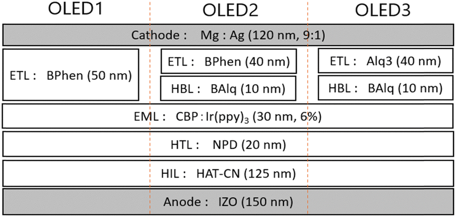 | ||
| Fig. 1 Schematic of the structure of the three bottom-emission OLEDs fabricated in this study. | ||
 | ||
| Fig. 2 (a) J–V characteristics of three OLED devices (OLED1, OLED2, and OLED3) used in this study. (b) Emission spectra of each OLED device at a current level of 0.15 mA. Emission intensities are normalized to the intensity at 515 nm. | ||
ESFG spectroscopy was conducted to investigate the charge behavior and electronic structure at the interfaces of the OLED devices under operating conditions. Similar to that in EFI-SHG, the intensity of the generated SFG light can be determined using eqn (1).24–26
| IESFG(ωsum) ∝ |χ(2) + χ(3)E0|2Iω1Iω2, | (1) |
A double-resonance vibrational SFG system31–35 was modified in this study to perform ESFG spectroscopy. A mode-locked Nd:YAG laser (PL2251C-10, EKSPLA, Lithuania) with a pulse width of 25 ps at 1064 nm and a 10 Hz repetition rate was used as the light source. Tunable visible light was generated using an optical parametric generator (PG411, EKSPLA, Lithuania) pumped with the third-harmonic light of the YAG laser. The ESFG signal was generated in the area where the frequency-tunable visible and near-IR beams at 1064 nm overlapped with incidence angles of 70° and 62°, respectively, from the surface normal. Irradiating the near-infrared 1064 nm light incident at this angle allows the vibrational SFG detection system to be used as an ESFG detection system without changing the optical setups. The SFG light was detected using a photomultiplier (R649; Hamamatsu Photonics K.K., Japan) after passing through a short-wave pass filter (Asahi Spectra Co. Ltd, Japan), prism monochromator (PF-200, Bunkoukeiki Co., Ltd, Japan), and grating monochromator (MS2001i; SOL Instruments, Belarus). The signal was averaged over 250 pulses with a gated integrator for every data point taken at 10 nm intervals and stored on a personal computer. Visible light was varied from 420 to 670 nm. The spectral resolution of the tunable visible beam was approximately 8 cm−1, and its frequency was calibrated using Hg lines. The output light generated by irradiating 1064 nm and visible light simultaneously is not two-photon fluorescence but ESFG, which is confirmed by measuring the output angle and the spectral width of the generated light by irradiating the OLEDs (Fig. S2 in the ESI†). Each ESFG spectrum was normalized to the visible and near-infrared powers to compensate for laser intensity fluctuations. The ESFG spectra were measured by illuminating visible and near-infrared lights from the CaF2 transparent substrate side, where the transparent IZO anode is located. Because this study focused on the electric field normal to the samples, all ESFG spectra were collected using a p-polarized SFG, p-polarized 1064 nm, and p-polarized visible beam (ppp) combination. To perform ESFG spectroscopy under the operating conditions, a DC power source (PMC18-2A; Kikusui Electronics Co., Japan) was used to apply bias voltages to the OLED samples. The diameter of the laser spot is approximately 1 mm. The samples were inspected to determine whether repeated measurements damaged them.
Details of the time-resolved SFG via square-wave pulse bias are described in our previous paper.33 In the time-resolved ESFG experiments, the multilayer OLEDs were operated with the application of a square-wave pulse voltage using a pulse delay generator (DG535, Stanford Research Systems, USA) and a high-speed bipolar amplifier (HSA4101, NF Co. Japan). Transient EL Emission from the OLEDs was detected using a photomultiplier (H10721, Hamamatsu) equipped with a high speed preamplifier (C9999, Hamamatsu) and was stored in an oscilloscope (TDS-2022C, Tektronix, USA).
Results and discussion
The ESFG spectra correspond to the ultraviolet (UV)–visible absorption spectra at the interfaces because they provide light responses of the frequencies of the sum of the wavelength-tunable visible and near-infrared light. Therefore, the absorption bands observed in the ESFG spectra can be attributed to the optical UV–visible absorption spectra of the corresponding materials at the interfaces. Fig. 3(a)–(c) shows the ESFG spectra of OLED1, 2, and 3 under various applied voltages. The ESFG-subtracted spectra between the ESFG spectra at 0 V for each OLED and the ESFG spectra of the devices at applied forward bias voltages are plotted in Fig. 3(d)–(f) to observe the changes in the ESFG responses with the applied voltages. We note that the measurement at 0 V is carried out with both electrodes being electrically connected and is not an open-circuit condition. Under open-circuit conditions, the impact of the contact potentials between the electrodes and the organic material is hard to distinguish from the potential difference between the two electrodes. Consequently, by subtracting the ESFG spectrum of the closed circuit (0 V) from the ESFG spectra with applied voltages, it is possible to observe the changes in the ESFG spectra attributable to the potential difference between the two electrodes and the behavior of the internal electric field within the devices. At an incident visible wavelength of 420–670 nm, the ESFG wavelength that occurs upon irradiation with 1064 nm near-infrared light is approximately 300–410 nm. In Fig. 3(g), a simulated transmission spectra of the organic multilayer film based on the optical absorption spectra of OLED1 materials are shown. It indicates that HAT-CN has strong optical absorption in the short wavelength region. Consequently, the absence in the intensity of the ESFG spectra in the region from 300 to 330 nm is presumably due to the influence of the absorption of the HAT-CN layer.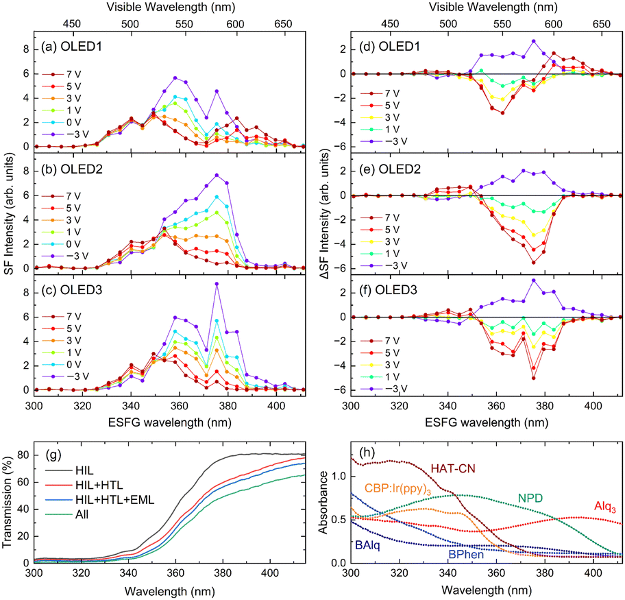 | ||
| Fig. 3 (a)–(c) Applied voltage dependence of the ESFG spectra of OLED1, OLED2, and OLED3. (d)–(f) Subtracted ESFG spectra of OLED1, 2, and 3 with respect to those of 0 V. (g) Simulated transmittance spectra in the UV region for each of the HIL layer, HIL + HTL layers, HIL + HTL + EML layers, and all organic layers when stacked, based on the absorption spectra of each layer of OLED1. (h) Optical absorption spectra of each OLED material at a film thickness of 100 nm. | ||
When a forward bias is applied, the ESFG of OLED1 shows an increase in the intensity of the ESFG wavelength from 380 to 400 nm, whereas a decrease in the intensity is observed in the 350 to 380 nm wavelength region. From the UV–visible optical absorption spectra of each OLED material shown in Fig. 3(h), the wavelength region where the decrease in the intensity of the ESFG band around 360 nm overlaps with the absorption edge of CBP is commonly used as the EML host material for these OLEDs. It is reasonable to interpret that this ESFG band is derived from CBP, since the band gap of the CBP coincides with 350 to 380 nm.44 Note that this band was not derived from HAT-CN because no ESFG signals were detected in this measurement region in the 100 nm thick HAT-CN deposited film (Fig. S3 in the ESI†). The detailed reason for this requires further verification, but we suspect that the molecular orientation of the HAT-CN-deposited film may have taken a horizontal orientation that does not allow the detection of ESFG signals.45 In addition to this, it is also possible that the ESFG of HAT-CN could not be observed because of the optical process of ESFG. The ESFG optical process requires both two-photon absorption and optical transition.46 HAT-CN has D3h symmetry, which causes its two-photon absorption peak position to be different from the one-photon absorption peak position,47,48 unlike that observed for other molecules used in OLEDs.
In OLED2 and OLED3, in addition to the decrease in ESFG intensity around 360 nm owing to the voltage applications observed in OLED1, a decrease in ESFG intensity around 380 nm was also observed with voltage application. Although the ETL materials of these two devices are different, the subtracted ESFG spectra are similar. The only difference between the device configurations of OLED1 and OLED2 is that the 50 nm thick BPhen is replaced by the combination of 40 nm thick BPhen and 10 nm thick BAlq, and hence the changes in ESFG intensities around 380 nm are certainly due to the insertion of the hole-blocking BAlq layer. The UV–VIS absorption spectrum of BAlq also suggests that the absorption edge of BAlq in this region is approximately 380–400 nm. Note that to precisely evaluate the difference in SFG signal intensities, multiple reflection effects should be taken into account. However, the total thickness of the three types of devices is equal, and the difference in the refractive indices of the organic materials is small. Hence, neglecting the effects of multiple reflection, the differences in the ESFG spectra of these devices clearly indicate that they are correlated with the presence or absence of the BAlq. Therefore, we conclude that the band around 380 nm is derived from the hole-blocking BAlq.
On the other hand, the bands at 370–400 nm, where the ESFG signal intensities in OLED1 increased with the applied voltage, are considered to originate from NPD, a hole-transport material, as compared to the optical absorption from NPD. Taguchi et al.21 reported that the EFI-SHG signal intensity in the wavelength region from 400 to 500 nm, which was derived from NPD in the EFI-SHG spectra of bilayer OLEDs consisting of Alq3 and NPD, increased with increasing applied voltage. The SHG band of NPD was extended to wavelengths shorter than 400 nm, which overlapped well with the wavelength detected in this study. In our previous study on OLED1 using EFI vibrational SFG,35 the intensities of the vibrational bands derived from the NPD molecules increased because of the electric-field-induced effect caused by the accumulated charges at the EML/HTL interfaces. Thus, it can be concluded that the increase in the intensities of the ESFG signals derived from the NPD interface is due to the electric field-induced effect caused by the accumulated charges at the NPD layer, as reported in our previous study.35 Here, we note that an ESFG band that does not show any response to the applied voltage in the region of 340–370 nm is observed in all three devices. At present, the assignment of this band is unclear; however, it is possible to be an ESFG band derived from the electronic transitions of their common interface.
According to eqn (1), the electric-field-induced ESFG signal intensity is expected to increase roughly quadratically with respect to E0. Hence, the applied voltage dependence of the ESFG signal intensities at the representative wavelengths was investigated. In Fig. 4, the applied voltage dependence of the  intensities at four representative visible wavelengths are plotted for the three different OLEDs. Although the voltage dependence differed depending on the OLED device configuration, the square-root ESFG intensities were almost linearly related to the applied voltages, as shown in Fig. 4. It is interesting to note, however, that even at the same wavelength, the voltage at which the ESFG intensity reaches a minimum varies from device to device. The behavior of these curves shown in Fig. 4 indicates that an electric field is present inside the device even under short-circuit conditions (0 V), which is presumably related to both the spontaneous orientational polarization of the inner organic layers of the device33,49,50 and the energy level alignment between different organic layers, since the built-in potential derived from the electrodes of these three devices are identical because of the fact that the electrode materials are the same for these devices. The fact that the voltage that yields the minimum ESFG signal intensity varies with the ESFG wavelength indicates that the electric-field information associated with different organic layers can be determined by employing different ESFG wavelengths. As shown in Fig. 4, the voltage dependence of the ESFG intensities at each wavelength exhibits a similar behavior for OLEDs 2 and 3, whereas only OLED1 exhibits a different behavior. Because the common device configuration of OLED2 and 3 is a 10 nm-thick BAlq inserted as a hole-blocking layer, these observations suggest that the electrical potential balance inside the OLED device is changed by the insertion of BAlq. Although the J–V characteristics shown in Fig. 2 indicate a substantial difference between OLED2 and OLED3, the applied voltage dependence of the ESFG signals exhibits a similar trend. This observation suggests that the electric field environments at each organic interface in OLED2 and OLED3 are similar. Indeed, it has been reported that BAlq has a relatively large permanent dipole moment than NPD and that it shows spontaneous orientation polarization via formation of thin films.51 This means that the presence of the spontaneous orientation polarization of BAlq changes the potential balance of each layer in the OLED device even under the short-circuit conditions. The fact that inserting thin BAlq layers alters the voltage dependence of the NPD-derived ESFG is very interesting, since it cannot be explained by the built-in potential caused by the difference in the work function between the two electrodes or the energy diagrams shown in Fig. S1 (ESI†).
 | ||
| Fig. 4 Applied voltage dependence of the square root of the ESFG signal intensity variations for the three OLED devices at fixed representative visible wavelengths. | ||
Next, time-resolved experiments were performed to investigate the charge-carrier behavior in the OLEDs in more detail. The use of the time-resolved technique allowed us to investigate whether charge carrier generation and transport inside the organic devices varied with time in response to the applied square-wave pulse bias voltage. In Fig. 5, the temporal response of the ESFG signal intensities with the applied pulse bias for OLED1 for visible wavelengths from 470 to 670 nm is illustrated. As shown in Fig. 5(a), a square-wave pulse bias of +12 V with a width of 15 μs was applied to ensure a sufficient current value for light emission from the OLED devices. For comparison, transient EL emissions collected simultaneously were also provided in Fig. 5(a). In the time-resolved experiments, we should note that the discrepancy between the transient ESFG spectra sliced in the vertical direction of the time-resolved spectra and the steady-state ESFG spectra with applied voltage shown in Fig. 3 is due to the difference in the amount of time required for the measurements. In the steady-state measurements, the time required for each spectrum was about 15 min, whereas the time required for each wavelength was more than 1 h in the time-resolved measurements. Thus, the fluctuations in the visible laser wavelength between neighboring wavelengths were relatively large in the time-resolved experiments. The dips at 540, 590, 620, and 660 nm are due to this laser fluctuation caused by the OPG laser system. As shown in Fig. 5(b) and (c). the NPD-derived bands in the visible excitation wavelength region from 590 to 670 nm (EFG of 380–410 nm) increased immediately after the pulse bias was applied. Most interestingly, the ESFG intensities in the visible excitation wavelength region of 540 nm (EFG of 360 nm), which originates from the CBP host material of the EML, show a decrease in the intensity immediately after the application of the pulse voltage, and then gradually increase in the intensity. This unique behavior of ESFG intensities was also observed in the fall-edge region. Considering these time-response behaviors from the device structure of OLED1, holes are immediately injected into the NPD layer owing to the charge separation at the interface between NPD and HAT-CN at the rise-edge of the pulse voltage; therefore, the ESFG band of NPD is increased by the electric field formed by the positive charges. However, in the EML, no charges are injected immediately after the pulse voltage is applied, and the polarization charges derived from the spontaneous orientation polarization that originally existed in the device33,49,50 are canceled by the external electric field, resulting in a rapid decrease in the ESFG signal intensities. Then, the injected charges proceed through inside the device, and when they reach the EML, an electric field is formed by the positive charge in the NPD layer and the negative charge injected into the EML, and this electric field formed in between induces the increase in the ESFG band intensity of the CBP in the host of the EML with time. Thereafter, since electrons and holes that reach the EML combine to form excitons and emit luminescence within the layer, the increase in the electric field within the EML reaches saturation. In the fall-edge region shown in Fig. 5(b) and (d), the internal electric fields formed inside the EML by the injected charges disappear with the vanishing of both positive and negative charges, and then the electric fields inside the device return to their original states, which are formed by the polarization charges and built-in potentials.
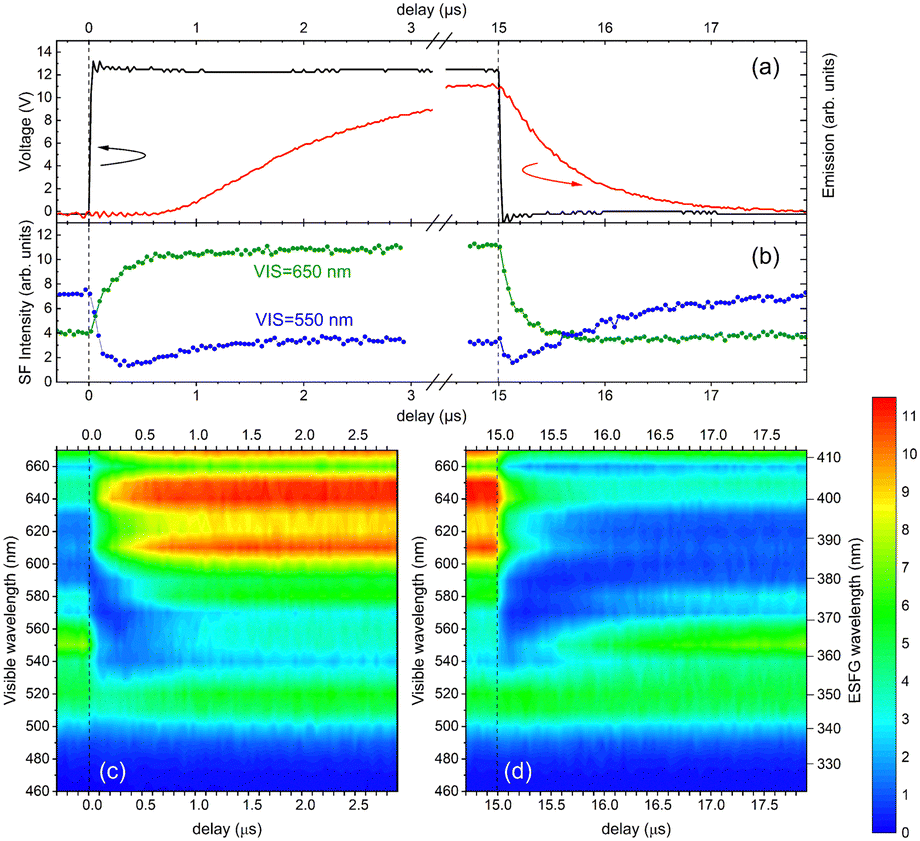 | ||
| Fig. 5 (a) Transient EL emission (red) from OLED1 under application of the square-wave pulse bias (black) of +12 V (pulse width of 15 μs). (b) Transient ESFG intensities of OLED1 at the visible wavelengths of 650 (green) and 550 nm (blue). Time-resolved ESFG intensity variations in the visible excitation wavelength region of 460–670 nm for the OLED1 (c) turn-on and (d) turn-of. | ||
Then, are there any differences between OLED1 and the other two OLED devices with respect to the time response of the ESFG signals when a pulse bias is applied? Fig. 6 shows the time responses of the rise and fall edges of the ESFG signals as well as the transient EL emissions of OLED2 and OLED3. At the longer-wavelength side of the visible wavelength region from 590 to 670 nm (ESFG wavelength from 380 to 410 nm), the ESFG signal intensities increased with the application of the pulse voltage in OLED1, whereas the ESFG signals in OLED2 and OLED3 tended to decrease with the application of the pulse voltage and then gradually increased in the ESFG intensities (detailed time response of the ESFG intensities are shown in Fig. S4 in the ESI†). One possible explanation is due to the overlapping of the BAlq absorption band with that of NPD, and the BAlq ESFG band decreases in intensity before the intensity changes of NPD caused by pulse bias application. On the other hand, if the concentration of the injected holes in the NPD layer is equivalent in OLED1 and the other two OLEDs when the same bias voltage is applied, the increase in the ESFG intensity from the NPD band should be more pronounced even in OLED2 and OLED3; however, as shown in Fig. 6(b), the ESFG intensities of the NPD of these devices are not increased as much as in OLED1. These results suggest that the electric field inside the NPD layer is smaller in OLED2 and OLED3 than in OLED1, presumably because the insertion of the thin layer of BAlq changes the potential balance inside the device. In other words, the insertion of the BAlq layer reduces the number of holes inside the NPD layer, thus suppressing the increase in the ESFG band strength of the NPD owing to charge injection. This is also inferred from the fact that the insertion of the BAlq layer leads to a slow rise in transient EL emission (Fig. S5, ESI†), which means that the number of charges in the OLEDs at the same time is different between OLED1 and the other two devices.
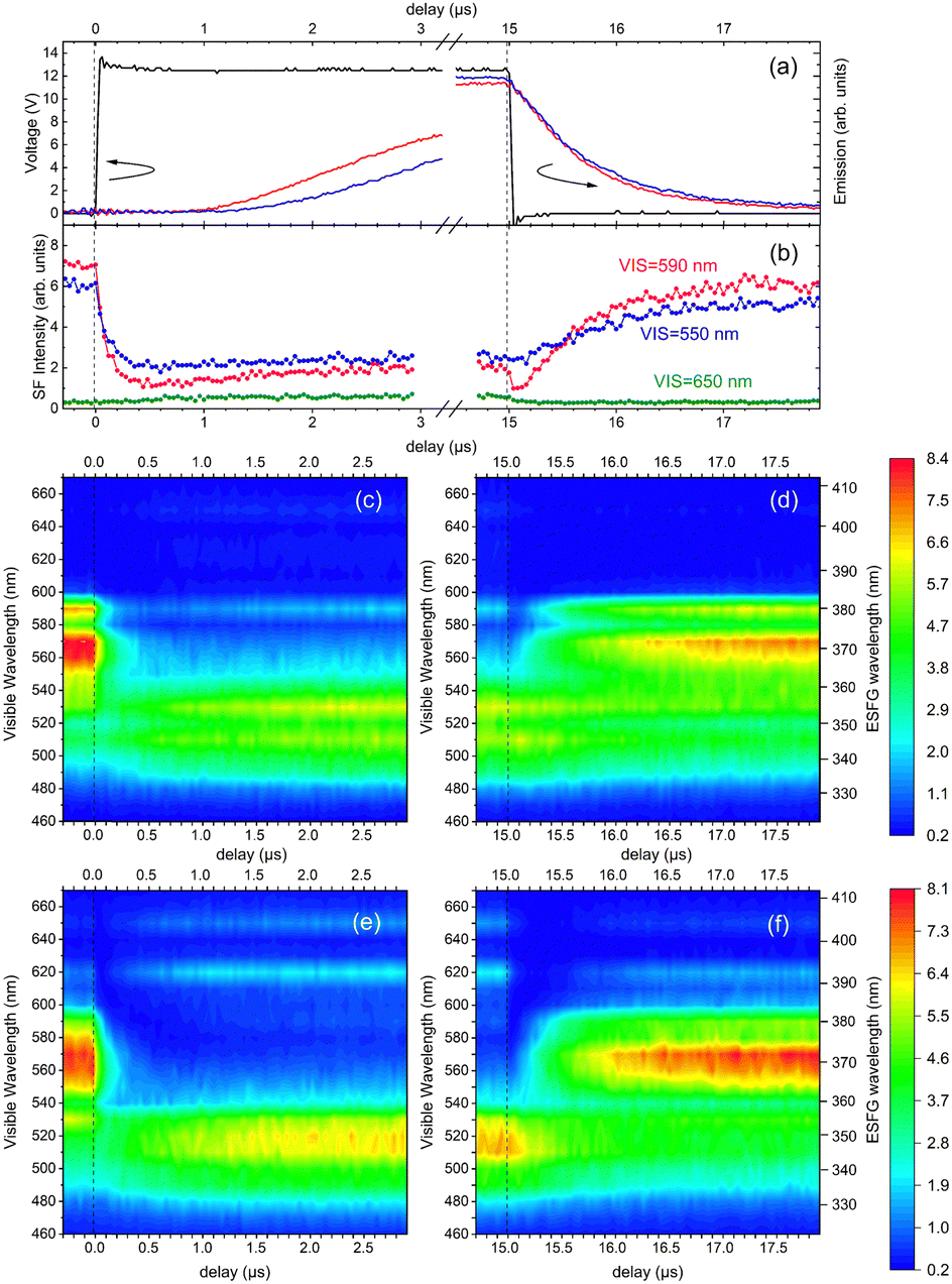 | ||
| Fig. 6 (a) Transient EL emission from OLED2 (red) and OLED3 (blue) under application of the square-wave pulse bias (black) of +12 V (pulse width of 15 μs). (b) Transient ESFG intensities of OLED2 at the visible wavelengths of 650 (green), 590 (pink), and 550 nm (blue). Time-resolved ESFG intensity variations of the OLED2 (c) turn-on and (d) turn-off. Time-resolved ESFG intensity variations of the OLED3 (e) turn-on and (f) turn-off. | ||
In contrast, the BAlq layer is strongly influenced by the voltage application in the voltage response of the ESFG of OLED2 and 3, which is also reflected in the time response of the ESFG band intensity around 370 nm in the time-resolved measurements. This is inferred from the prominent ESFG time response of the BAlq band at 370 nm, in addition to the voltage response of the CPB band of the EML observed at 360 nm. In other words, the negative charge may remain in the BAlq layer during the voltage application. This hypothesis is further confirmed by the EL emission spectra of the three OLED devices. To confirm the differences in the emission spectra of OLED1, 2, and 3, the applied voltage dependence of their emission spectra is shown in Fig. 7. The intensities of the emission peak at a shorter wavelength at 500 nm for OLED2 and OLED3 with a 10 nm-thick BAlq layer are notably stronger than those of the 550 nm peak as compared to the OLED1 device without BAlq. It should be noted that the difference in the shape of the emission spectra of OLED1 and the other two devices is not due to the differences in the applied voltage or the current levels, because the shape of the emission spectra does not change when the voltage applied to each device is changed, as shown in Fig. 7. In addition, since these devices are bottom-emission type OLEDs, we should note that the emission spectral shapes are not significantly modified by the cavity effect as observed in the top-emission type OLEDs.35 Nevertheless, changes in the emission spectral shapes due to the insertion of a 10 nm-thick BAlq layer suggests that the contribution of luminescence at the BAlq interface needs to be considered. Although BAlq acts as an HBL in general, it has also been reported that BAlq can be used as an emission material.52–54 Consequently, both holes and electrons can penetrate the BAlq layer. Because holes reach the BAlq HBL interface in OLEDs incorporating BAlq, it is suggested that excitons are formed in the EML/HBL interphase region under the operating conditions of these OLEDs. Because the electroluminescence emission of BAlq has a peak at approximately 500 nm,53 it can be concluded that it is emitted at the EML/HBL interface in OLED2 and OLED3. Thus, we conclude that these differences in the emission sites are reflected in the differences in the EL emission spectral shapes.
 | ||
| Fig. 7 Applied voltage dependence of the emission spectra of OLED1, OLED2, and OLED3. | ||
The above hypothesis can also be understood from the difference in the current efficiency of each device shown in Fig. 8. In OLED1, a significant roll-off is observed in the high current density region, whereas such a roll-off phenomenon becomes smaller in OLED2 and OLED3. It has been suggested that such roll-off behavior can be reduced by altering the charge carrier balance within the OLED device and changing the light emission region.55 In fact, the roll-off observed in OLED1 is reduced in OLED2 and 3, as shown in Fig. 8, and this can be interpreted as being due to a change in the charge balance within the OLED and a change in the light emission region, which supports our hypothesis. These differences are due to the insertion of the thin BAlq layer, but it is not easy to observe these differences directly using other measurement techniques. One of the greatest advantages of the ESFG technique is that it reveals these differences as differences in the voltage response in the corresponding wavelength regions of the spectra for each material.
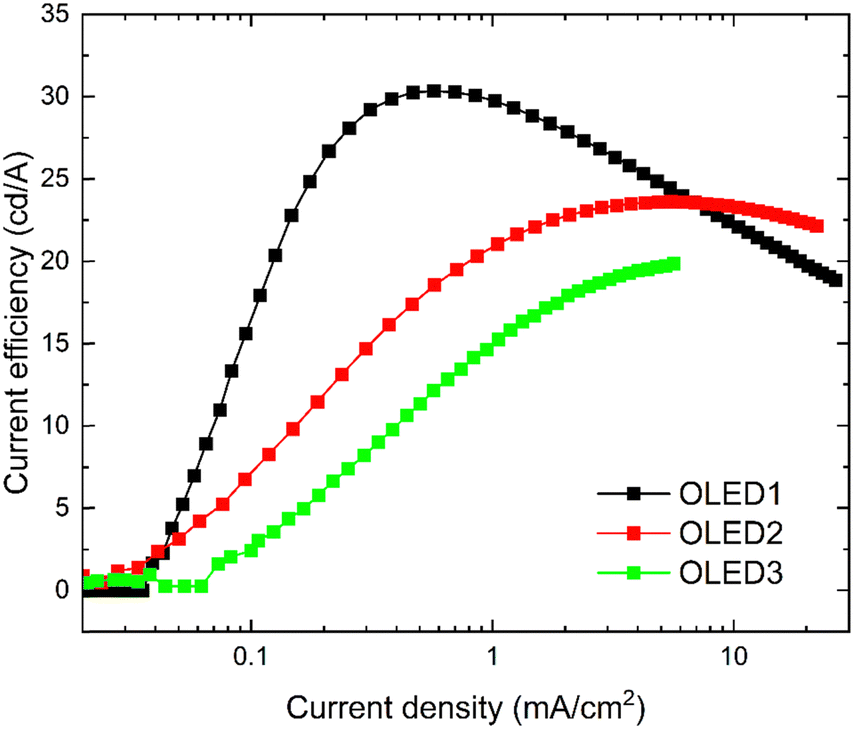 | ||
| Fig. 8 Current efficiencies of the three OLED devices. Note that the luminance measurements are only taken from the front of the devices, so they are not external quantum efficiencies. | ||
Conclusions
ESFG spectroscopy of OLEDs under different operating conditions was conducted to observe the spectral changes caused by current injection into the OLED interfaces. The assignments for the ESFG bands of each organic layer were determined by referring to the optical absorption spectra and the layer configurations of the devices. Changes in the ESFG signal intensities were successfully observed by applying voltages to the OLED devices, which were associated with changes in the electric field and charge injection in the EML. The ESFG spectra of OLED devices with different configurations are very useful for identifying the differences in the intensities of the internal electric fields formed at the HTL, EML, and HBL. The applied voltage responses of the ESFG spectra reveal the differences in the strengths of the electric fields inside the OLED devices caused by the organic layers that comprise the devices, which lead to the differences in the ease of internal charge flow and emission properties. Using time-resolved ESFG measurements with square-wave pulse voltages, it is confirmed that the insertion of BAlq changes the position of the light emission with the injected charges, which explains well the differences in the emission spectral shapes and the current efficiencies between the devices. This technique represents a novel and highly effective nondestructive spectroscopic approach for probing the electric field generation caused by injected charges in solid-state thin-film devices.Author contributions
The manuscript was written through contributions of all authors. All authors have given approval to the final version of the manuscript. T. K., K. M., and T. M. conceived the research. T. K. and K. M. carried out the data curation and analyses. T. M. supervised the research, established funding for the research, and provided contributions to interpreting the results and drafting the manuscript.Data availability
All the data presented in the paper are available upon request from the authors.Conflicts of interest
There are no conflicts to declare.Acknowledgements
We thank LG Japan Lab. Inc. for providing the OLED devices. This study was partially supported by JSPS KAKENHI Grants-in-Aid for Scientific Research (grant numbers 22H02048 and 23K17811), Japan.Notes and references
- T. Tsujimura, OLED Display Fundamentals and Applications, John Wiley & Sons, Inc., USA, 2017 Search PubMed.
- J. Bauri, R. B. Choudhary and G. Mandal, J. Mater. Sci., 2021, 56, 18837–18866 CrossRef CAS.
- C. W. Tang and S. A. VanSlyke, Appl. Phys. Lett., 1987, 51, 913–915 CrossRef CAS.
- A. Endo, M. Ogasawara, A. Takahashi, D. Yokoyama, Y. Kato and C. Adachi, Adv. Mater., 2009, 21, 4802–4806 CrossRef CAS PubMed.
- H. Nakanotani, T. Higuchi, T. Furukawa, K. Masui, K. Morimoto, M. Numata, H. Tanaka, Y. Sagara, T. Yasuda and C. Adachi, Nat. Commun., 2014, 5, 4016 CrossRef CAS PubMed.
- T. Suzuki, Y. Nonaka, T. Watabe, H. Nakashima, S. Seo, S. Shitagaki and S. Yamazaki, Jpn. J. Appl. Phys., 2014, 53, 052102 CrossRef CAS.
- D. Y. Kondakov, Philos. Trans. R. Soc., A, 2015, 373, 20140321 CrossRef PubMed.
- S. J. Cha, N. S. Han, J. K. Song, A.-R. Park, Y. M. Jeon and M. C. Suh, Dyes Pigm., 2015, 120, 200–207 CrossRef CAS.
- T. Miyamae and T. Sato, J. Soc. Inf. Disp., 2023, 30, 3–14 CrossRef.
- Y. Noguchi, N. Sato, Y. Tanaka, Y. Nakayama and H. Ishii, Appl. Phys. Lett., 2008, 92, 203306 CrossRef.
- N. Alves and D. M. Taylor, Appl. Phys. Lett., 2008, 92, 103312 CrossRef.
- X.-W. Zhang, B.-J. Mo, L.-M. Liu, H.-H. Wang, D.-T. Chang, J.-W. Xu, H. Wang and B. Wei, Curr. Appl. Phys., 2014, 14, 1460–1464 CrossRef.
- Y. R. Shen, Nature, 1989, 337, 519–525 CrossRef CAS.
- Y. R. Shen, Fundamentals of Sum-Frequency Spectroscopy, Cambridge University Press, Cambridge, UK, 2016 Search PubMed.
- S. Ong, X. Zhao and K. B. Eisential, Chem. Phys. Lett., 1992, 191, 327–335 CrossRef CAS.
- P. Godefroy, W. Jong, C. W. Hasselt, M. A. C. Devillers and T. Rasing, Appl. Phys. Lett., 1996, 68, 1981–1983 CrossRef CAS.
- O. A. Aktsipetrov, A. A. Fedyanin, E. D. Mishina and A. N. Rubtsov, Phys. Rev. B: Condens. Matter Mater. Phys., 1996, 54, 1825–1832 CrossRef CAS PubMed.
- T. A. Germer, K. W. Kołasiński, J. C. Stephenson and L. J. Richter, Phys. Rev. B: Condens. Matter Mater. Phys., 1997, 55, 10694–10706 CrossRef CAS.
- T. Manaka, E. Lim, R. Tamura, D. Yamada and M. Iwamoto, Appl. Phys. Lett., 2006, 89, 1–4 CrossRef.
- T. Manaka, F. Liu, M. Weiss and M. Iwamoto, Phys. Rev. B: Condens. Matter Mater. Phys., 2008, 78, 1–4 CrossRef.
- D. Taguchi, M. Weiss, T. Manaka and M. Iwamoto, Appl. Phys. Lett., 2009, 95, 263310 CrossRef.
- D. Taguchi, L. Zheng, J. Li, M. Weiss, T. Manaka and M. Iwamoto, J. Phys. Chem. C, 2010, 114, 15136–15140 CrossRef CAS.
- D. Taguchi, T. Shino, L. Zhang, J. Li, M. Weiss, T. Manaka and M. Iwamoto, Appl. Phys. Express, 2011, 4, 021602 CrossRef.
- E. Lim, T. Manaka and M. Iwamoto, Chem. Phys. Lett., 2011, 516, 254–256 CrossRef CAS.
- H. Ye, J. Huang, J. R. Park, H. E. Katz and D. H. Gracias, J. Phys. Chem. C, 2007, 111, 13250–13255 CrossRef CAS.
- I. F. Nakai, M. Tachioka, A. Ugawa, T. Ueda, K. Watanabe and Y. Matsumoto, Appl. Phys. Lett., 2009, 95, 243304 CrossRef.
- T. C. Anglin, D. B. O’Brien and A. M. Massari, J. Phys. Chem. C, 2010, 114, 17629–17637 CrossRef CAS.
- T. C. Anglin, Z. Sohrabpour and A. M. Massari, J. Phys. Chem. C, 2011, 115, 20258–20266 CrossRef CAS.
- S. G. Motti, L. S. Cardoso, D. J. C. Gomes, R. M. Faria and P. B. Miranda, J. Phys. Chem. C, 2018, 122, 10450–10458 CrossRef CAS.
- C. Katagiri, T. Miyamae, H. Li, F. Yang and S. Baldelli, Phys. Chem. Chem. Phys., 2021, 23, 4944–4950 RSC.
- T. Miyamae, N. Takada and T. Tsutsui, Appl. Phys. Lett., 2012, 101, 073304 CrossRef.
- T. Miyamae, N. Takada, T. Yoshioka, S. Miyaguchi, H. Ohata and T. Tsutsui, Chem. Phys. Lett., 2014, 616–617, 86–90 CrossRef CAS.
- T. Miyamae, N. Takada, H. Ohata and T. Tsutsui, Appl. Phys. Express, 2017, 10, 102101 CrossRef.
- T. Sato, T. Miyamae, H. Ohata and T. Tsutsui, Org. Electron., 2019, 74, 118–125 CAS.
- K. Morimoto, T. Kaburagi, H. Ohata, S. Noh and T. Miyamae, Org. Electron., 2023, 120, 106862 CAS.
- S. Yamaguchi and T. Tahara, J. Phys. Chem. B, 2004, 108, 19079–19082 CAS.
- Y. Li, J. Wang and W. Xiong, J. Phys. Chem. C, 2015, 119, 28083–28089 CAS.
- G.-H. Deng, Y. Qian and Y. Rao, J. Chem. Phys., 2019, 150, 024708 Search PubMed.
- R. Pandey, A. P. Moon, J. A. Bender and S. T. Roberts, J. Phys. Chem. Lett., 2016, 7, 1060–1066 CAS.
- D. E. Cotton, A. P. Moon and S. T. Roberts, J. Phys. Chem. C, 2020, 124, 11401–11413 CAS.
- G.-H. Deng, Y. Qian, Q. Wei, T. Zhang and Y. Rao, J. Phys. Chem. Lett., 2020, 11, 1738–1745 CAS.
- Y. Kumar, S. Dhami and R. Pandey, Biointerphases, 2023, 18, 041202 CAS.
- W. Jeoung, S. Y. Kim, J. J. Kim and J. W. Kang, Chem. Phys., 2009, 355, 25–30 Search PubMed.
- N. Matsusue, S. Ikame, Y. Suzuki and H. Naito, J. Appl. Phys., 2005, 97, 123512 Search PubMed.
- H. J. Kim, J. H. Lee, J. W. Kim, S. Lee, J. Jang, H. H. Lee and J. J. Kim, J. Mater. Chem. C, 2013, 1, 1260–1264 CAS.
- G. J. Simpson, Nonlinear Optical Polarization Analysis in Chemistry and Biology, Cambridge University Press, Cambridge, UK, 2017 Search PubMed.
- D. Beljonne, W. Wenseleer, E. Zojer, Z. Shuai, H. Vogel, S. J. K. Pond, J. W. Perry, S. R. Murder and J. L. Brédas, Adv. Funct. Mater., 2002, 12, 631–641 CAS.
- J. L. Segura, R. Juárez, M. Ramos and C. Seoane, Chem. Soc. Rev., 2015, 44, 6850–6885 CAS.
- Y. Noguchi, Y. Miyazaki, Y. Tanaka, N. Sato, Y. Nakayama, T. D. Schmidt, W. Brütting and H. Ishii, J. Appl. Phys., 2012, 111, 114508 Search PubMed.
- Y. Noguchi, H. Lim, T. Ishoshima, E. Ito, M. Hara, W. W. Chin, J. W. Han, H. Kinjo, Y. Ozawa, Y. Nakayama and H. Ishii, Appl. Phys. Lett., 2013, 102, 203306 Search PubMed.
- Y. Noguchi, W. Brütting and H. Ishii, Jpn. J. Appl. Phys., 2019, 58, SF0801 CrossRef CAS.
- Y. Iwama, T. Itoh, T. Mori and T. Mizutani, Thin Solid Films, 2006, 499, 364–368 CrossRef CAS.
- T. Itoh, T. Mizutani and T. Mori, Colloids Surf., A, 2006, 284, 594–598 CrossRef.
- S. L. M. Mensfoort, R. J. Vries, V. Shabro, H. P. Loebl, R. A. J. Janssen and R. Coehoorn, Org. Electron., 2010, 11, 1408–1413 CrossRef.
- C. Murawski, K. Leo and M. C. Gather, Adv. Mater., 2013, 25, 6801–6827 CrossRef CAS.
Footnote |
| † Electronic supplementary information (ESI) available. See DOI: https://doi.org/10.1039/d4tc04970e |
| This journal is © The Royal Society of Chemistry 2025 |