
 Open Access Article
 This Open Access Article is licensed under a Creative Commons Attribution-Non Commercial 3.0 Unported Licence
Plasmon-enhanced organic field effect transistors
Navneet
Kumar
 a,
Howe R. J.
Simpson†
b,
Md Masud
Rana†
a and
Karthik
Shankar
*a
a,
Howe R. J.
Simpson†
b,
Md Masud
Rana†
a and
Karthik
Shankar
*a
aElectrical and Computer Engineering Department, University of Alberta, Edmonton, AB T6G 1H9, Canada. E-mail: kshankar@ualberta.ca
bDepartment of Physics, University of Alberta, Edmonton, AB T6G 2E1, Canada
First published on 3rd May 2025
Abstract
The low cost and ease of fabrication of organic electronics is often overlooked due to their lower performance parameters and poor stability under atmospheric conditions. Thus, steps need to be taken to improve technology in meaningful ways to compete with their inorganic counterparts. In this context, the integration of plasmonic materials and nanostructures into the channel or gate dielectric of organic field transistors (OFETs) enables improvements in the performance and function of phototransistors, transistor-based optical memory devices, organic light emitting transistors (OLETs) and organic electrochemical transistors (OECTs). Plasmonic nanoparticles have been used to fabricate the floating gate of FET memory devices and generate adaptable shifts in the threshold voltage. The detection sensitivity of OECTs was enhanced by the local electromagnetic field enhancement effect and improved electron transfer effect associated with gold nanoparticles integrated into the OECT. Schottky barrier phototransistors integrated with chiral plasmonic nanoparticles enable detection of circularly polarized light. In OLETs, integration with surface plasmons improves local electroluminescence yields as well as the directionality of emission and the light outcoupling efficiency. Graphene plasmons achieved strong confinement of THz radiation and thus enabled gated terahertz detectors.
 Navneet Kumar | Navneet Kumar received his Bachelor of Engineering degree in Electrical and Electronics Engineering from Manipal University, Karnataka, India in 2012. He subsequently worked as a Service Engineer in GE Healthcare for 6 years. He completed his MS degree in Electrical and Computer Engineering at the University of Illinois at Chicago in 2019. He is currently a PhD candidate at the University of Alberta in Electrical and Computer Engineering. His research interests include plasmonics, microwave resonators, metal-oxide semiconductors for photocatalysis, organic semiconductors, electrochromic devices and hybrid solar cells. |
 Howe R. J. Simpson | Howe Simpson completed his Bachelor's degree with Honors in Physics at Dalhousie University in Halifax, Nova Scotia, Canada in 2019. He then completed his MSc in Physics in 2021 at the University of Alberta with a focus on using terahertz scanning tunneling microscopy on superconductor and metal surfaces. Currently, he is completing his PhD degree in Physics at the University of Alberta continuing his research using a terahertz scanning tunneling microscope with a focus on semiconductor–metal interfaces and silicon dangling bond dynamics. |
 Md Masud Rana | Md Masud Rana received a BSc degree in Electrical and Electronic Engineering from Chittagong University of Engineering and Technology (CUET), Bangladesh with distinction in 2012. Later he received an MSc degree in Electrical and Electronic Engineering from Khulna University of Engineering and Technology (KUET), Bangladesh with excellence in 2019. Now he is pursuing his PhD degree in Electrical and Computer Engineering at the University of Alberta, Canada while specializing in solid-state electronics. Prior to joining the PhD program at the University of Alberta, he was appointed as a lecturer in the Department of Electrical and Electronic Engineering at Jashore University of Science and Technology (JUST), Bangladesh and was recently promoted to Assistant Professor. He is researching organic semiconductors, bismuth oxyhalide nanomaterials and plasmonic nanomaterials for generating solar fuels through photoelectrochemical water splitting, photocatalytic hydrogen generation and CO2 photoreduction. |
 Karthik Shankar | Karthik Shankar is Professor of Electrical & Computer Engineering at the University of Alberta. He obtained his BTech degree in 2000 from the Department of Metallurgy and Materials Science at the Indian Institute of Technology Madras (IIT-M) in Chennai, India. He completed MS (2002) and PhD (2007) degrees in Electrical Engineering at the Pennsylvania State University. He was an Eastman Kodak research fellow at Penn State University. He joined the University of Alberta in 2009 as an Assistant Professor, and obtained early tenure and promotion to Associate Professor in 2013. He is a recipient of the Petro-Canada Young Innovator Award. He was promoted to Full Professor in 2018. He has authored over 180 journal articles that have collectively been cited more than 25 |
1. Introduction
The emergence of organic electronics has replaced conventional electronics in many fields. The displays and screens in select smartphones, laptops and televisions now contain organic light emitting diodes (OLEDs) with resultant low power consumption, very thin screens and higher contrast compared to the previously used liquid crystal displays (LCDs).1–4 The AMOLED (active-matrix OLED) displays employ an array of thin film transistors (TFTs) which control each pixel of the display and offer better resolution.5–7 Besides displays, organic electronic devices are also used in other technologies such as sensors, phototransistors, non-volatile memories, electronic textiles, wearable phototherapeutics and most recently in recording neuronal and brain activities.8–16 Sustained interest in organic transistors was sparked by the invention of a melanin based bistable switch by McGinness et al.17 and shortly thereafter, the discovery of high conductivity in doped polyacetylene by Shirakawa et al. in 1977,18 for which the Nobel Prize in Chemistry was awarded in 2000. The 1980s witnessed a flurry of activity in organic electronics and in 1986, Mitsubishi engineers Koezuka, Tsumura, and Ando reported the first organic field effect transistors (OFETs) based on polythiophene molecules.19Since organic semiconductors are bonded by weak van der Waals forces, the fabrication methods for thin film organic electronic devices are not as complex as those for inorganic semiconductors, the latter requiring conditions of extreme temperature and/or pressure in processes such as molecular beam epitaxy, chemical vapor deposition and single crystal growth. In addition, the decreased weight of organic semiconductors compared to Si based materials allows them to be used in lightweight and flexible electronic devices. However, the performance limitations of the organic transistor are still a matter of discussion in electronics research. For example, carrier mobilities and maximum drive current densities in organic thin film transistors (OTFTs) are inferior to their inorganic counterparts by a factor of 10–100.20 In spite of recent interest in organic bipolar transistors,21 the overwhelming majority of transistors with active layers consisting of π-conjugated small molecules or polymers are organic field effect transistors (OFETs) with metal source and drain electrodes and an insulating gate dielectric.22–25 Other technical problems associated with the use of organic semiconductors include engineering highly crystalline films with large sized grains, high sensitivity to ambient conditions and the unavailability of traditional doping methods to achieve a certain conduction type and conductivity.22–24,26 Processing additives as well as improved solution process techniques have positively impacted both the performance and ambient stability of OFETs.27–29 Different techniques to further enhance the performance of organic transistors are currently being explored. One such method is integrating coinage metal nanoparticles exhibiting localized surface plasmon resonances (LSPR) at visible and near-infrared (NIR) wavelengths with organic transistors.
Metals and quasi-metals are treated as plasmas given their positive ions are fixed in the lattice and a large number of delocalized negative charges (electrons) are free to move across the fixed positive ions. Under the influence of an applied electromagnetic field, the electron gas in a metal is displaced from the center of positive charge, resulting in a non-zero dipole moment. The positive ion background will then exert a restoring force on the electron gas, causing oscillations. The resonant frequency of these oscillations is called the plasma frequency, and the quantized plasma oscillations are known as volume (or bulk) plasmons. These volume plasmons arise in the bulk of the material and do not couple directly to transverse electromagnetic waves (such as light). At the dielectric–metal interface, that is at the surface of the metal, incident electromagnetic waves can couple to surface plasmons to form surface plasmon polaritons (SPPs), as shown in Fig. 1(a).30 The coupling has both a longitudinal and transverse mode, meaning for an SPP to couple to any incoming light care must be taken in preparing the metal surface to match the wave vector of the light using gratings or prisms. In contrast, excitations of surface plasmons can also be non-propagating if the applied electromagnetic field couples to the electrons of a metal or quasi-metal nanoparticle (NP).30,31 These excitations are known as localized surface plasmons. The curved shape of the sub-wavelength nanostructure both allows the direct excitation from light (without any surface preparation) to create charge density oscillations at the metal–dielectric interface, a phenomenon which is known as localized surface plasmon resonance (LSPR). Due to squeezing of electromagnetic energy previously carried by a photon into a much smaller mode volume at the nanoparticle surface, LSPR results in an enhancement of the electric field at the NP surface and in proximity to it as illustrated in Fig. 1(b).32,33 The magnitude of this enhancement depends on the shape, size, type of metal, distance between the individual NPs, and dielectric environment.34
 | ||
| Fig. 1 Surface plasmons (a) propagating along a metal/dielectric medium and (b) confined to a single nanoparticle. The need for a grating or a prism is shown in (a) to allow wavevector matching of the incident light to the resonance of the surface plasmon. In contrast, the nanoparticle in (b) allows both scattering of the incident light and an enhancement of the electric field in and close to the surface of the nanoparticle. Republished with permission of the Royal Chemical Society, from ref. 35; permission conveyed through Copyright Clearance Center, Inc. | ||
Along with the enhancement of the local electric field due to surface plasmon coupling either from SPPs or LSPR, surface plasmons are also able to concentrate light well past the diffraction limit.36 The dephasing of plasmons generates hot carriers with thermal equilibration times in the picosecond range.37,38 These properties of plasmons have been demonstrated to enhance the optoelectronic properties of inorganic and organic devices for applications such as waveguides,39–41 photodetectors,42,43 increasing power conversion efficiency in solar cells,44–46 driving chemical reactions,47,48 sensors,49,50 and actuators.51–54 The plasmon-mediated increase in oscillator strength also serves to enhance the fluorescence and Raman scattering signals.55–57
Cu, Al, Au, and Ag are commonly used as plasmonic materials given their surface plasmon resonances occur at visible and near-infrared wavelengths.58–60 Although Au and Ag are expensive noble metals compared to Cu and Al, they are still the metals of choice for surface plasmon coupling given Cu and Al suffer from chemical instabilities in atmospheric conditions as well as higher dielectric losses in the visible and near-infrared compared to Au and Ag, with Ag exhibiting the least loss.58 Coinage metal-free plasmon resonances are observed in nanoparticles and metasurfaces made of select chalcogenides and transition metal nitrides.61–67 Certain degenerately doped semiconductors and 2D materials also exhibit NIR plasmon resonances.68
The inclusion of plasmonic nanoparticles in organic semiconductor films allows for efficient light trapping and hot carrier generation resulting in higher current output from organic photovoltaic devices. Increases in performance parameters for different plasmon-coupled organic electronic materials and devices such as photoresponsivity and external quantum efficiency in organic photodiodes and phototransistors, drain current in organic transistors, faster spontaneous emission in organic fluorophores, and amplified light absorption capability in plasmon coupled organic semiconductors have also been reported.
In this review, we present the results and effects from the coupling of plasmons and organic semiconductors, with particular emphasis on plasmon-enhanced transistors. Five primary applications of plasmon-coupled transistors are discussed in detail: non-volatile memory devices using FETs, organic electrochemical transistors (OECTs) for sensing purposes, phototransistors with OSC channels, organic light emitting transistors (OLETs), and gated THz detectors exploiting graphene plasmons. We also discuss the underlying operating principle of these devices and compare performance metrics between pristine and plasmon-enhanced organic transistors. Silicon-based complementary metal oxide semiconductor field-effect transistors (CMOSFETs) suffer from limitations related to performance and functionality in the aforementioned applications. For instance, Si does not emit light, lacks memory behavior, exhibits weak light-matter interactions resulting in inefficient absorption and concomitant low e−–h+ pair creation, and is unable to respond to terahertz fields. In this review article, we show that integrating organic semiconductors (interpreted broadly to include graphene and its derivatives) with plasmonic nanoparticles enables new functionality and/or improved performance in niche optoelectronic applications.
2. Plasmon-coupled organic FET memory devices
OFET-based nonvolatile memory has attracted tremendous research interest in the field of organic electronics due to reliable data storage,11 nondestructive data readout and compatibility with organic logic circuits and flexible organic electronics.69–71 To boost the performance of the OFET memory, a floating-gate architecture is advantageous because of good memory retention and endurance, which are possible owing to the isolation of the carrier transport and charge storage layers with a tunneling dielectric in between them.72,73 Plasmonic NPs have been employed to fabricate the floating-gate in an OFET memory where the memory performance can be optimized by tailoring the size, density, and assembly of the NPs. Both monometallic and bimetallic plasmonic NPs have been used in the technical literature to form the floating gate. A bimetallic architecture produces an enlarged memory window in the OFET memory compared to its monometallic counterpart.The primary operating mechanism of OFET based memory devices is based on the adaptable shift of the threshold voltage (Vth).74 A bottom-gate top-contact architecture based OFET memory device is shown in Fig. 2(a), and consists of a floating-gate implanted in the gate dielectric of the OFET in conjunction with the controlling gate electrode. Upon application of the programming voltage to the gate to source terminal of the OFET, charges from the organic semiconductor channel layer are transferred to the floating-gate by direct tunnelling, or Fowler–Nordheim tunneling.75,76 The threshold voltage Vth of the transistor is changed from its initial value due to the charging of the floating-gate. The electric field exerted on the organic semiconductor channel through the application of a gate bias is altered due to the charges trapped in the floating-gate. The trapped charges in the floating-gate do not dissipate until an erasing voltage is applied because of the electrical isolation of the floating-gate. This is the basic action of non-volatile memory. On the other hand, when a voltage of opposite polarity to the programming voltage is applied to the gate to source terminal, the trapped charges on the floating-gate are discharged to the channel semiconductor. This time the threshold voltage Vth shifts in the opposite direction as the charging case. Consequently, a memory window is found in the OFET transfer characteristics.
 | ||
| Fig. 2 (a) Schematic illustration of OFET optical memory device (b) mechanism of carrier photogeneration, transport and trapping in the memory device, (c) TEM image of low aspect ratio Au@Ag NRs (Au@Ag NRs (A)), simulated electric field distribution of Au@Ag NRs (A) in PVPy layer (d) longitudinal and (e) transverse modes at 660 and 500 nm respectively and (f) UV-Vis spectra of the Au and Au@Ag NRs in aqueous solution. Reprinted (adapted) with permission from ref. 77 Copyright 2022 American Chemical Society. | ||
A schematic illustration of the plasmonic Au@Ag core–shell nanorods (NRs) based OFET optical memory is shown in Fig. 2(a). In this bottom-gate top-contact source/drain optical memory device, the floating-gate consists of cetyltrimethylammonium bromide (CTAB) capped core–shell gold–silver bimetallic nanorods dispersed in a polyvinylpyrrolidone matrix (PVPy-Au@Ag NRs) which acts as the charge trapping layer. For the fabrication of the OFET optical memory, it is crucial to employ broad spectrum photoresponsive materials. Au and Ag NPs are extensively used in photonic devices exploiting the localized surface plasmon resonance (LSPR) property.78 One of the vital features of the Au@Ag core–shell structure is that the plasmon resonance bands can be tuned/manipulated by varying the size of the Au core or the thickness of the Ag shell. As a result, a wide spectrum response ranging from the visible to near-infrared can be achieved. A p-type pentacene thin film is used as the channel material for the memory device owing to its crystallinity and concomitant high field-effect mobility, particularly when vacuum deposited onto polymeric gate dielectrics or self-assembled monolayer-coated inorganic substrates. The plasmonic enhancement of the optical memory and photodetector-type response of the device occurs through two different pathways. The first being the LSPR-mediated local field intensification resulting in higher optical absorption and exciton production in the pentacene channel, and secondly through selective trapping of photogenerated holes by the PVPy-Au@Ag NRs (Fig. 2(b)). The higher light absorption in the pentacene layer is due to the vertical extension of the longitudinal component, at 660 nm of the Au@Ag core–shell electric field. The generation, transport and trapping of photoexcited carriers in the memory device are shown in Fig. 2(b). The transmission electron microscopy (TEM) images of the low aspect ratio Au@Ag NRs are depicted in Fig. 2(c), whereas the simulated longitudinal and transverse electric field components are shown in Fig. 2(d) and (e), respectively. The UV-Vis spectra of Au NRs, Au@Ag NRs (A) and Au@Ag NRs (B) in aqueous solution are shown in Fig. 2(f). The optical absorption of the pristine Au NRs exhibits two distinct peaks corresponding to longitudinal and transverse surface plasmon resonances at 800 nm and 500 nm respectively. The longitudinal LSPR peak of the Au@Ag core–shell NRs blue-shifts with a decrease in aspect ratio of the Au@Ag NRs.
Fig. 3 demonstrates the electrical behavior of the Au@Ag NRs-PVPy based floating-gate p-channel OFET-based memory cells. ID–VGS curves of memory devices in the programmed state and erased state are shown in Fig. 3(a)–(e). Typically, vacuum deposited pentacene films have a non-negligible concentration of mobile holes at room temperature. When a programming voltage of −50 V over a duration of 1 s is applied to devices containing the plasmonic NRs, the transfer curve is dramatically shifted in the negative direction indicating a decrease (large negative shift) in Vth due to the transfer of holes from pentacene to the Au@Ag NRs enclosed in PVPy. The trapping of holes in the Au@Ag NRs-PVPy layer ensures that a more negative gate bias needs to be applied at the gate electrode to create an accumulation region in the channel (i.e. a more negative value of the turn-on voltage Vth). On the other hand, with the application of an erase voltage of +50 V for 1 s, the transfer curves are shifted back to their initial positions due to the detrapping of holes into the channel.
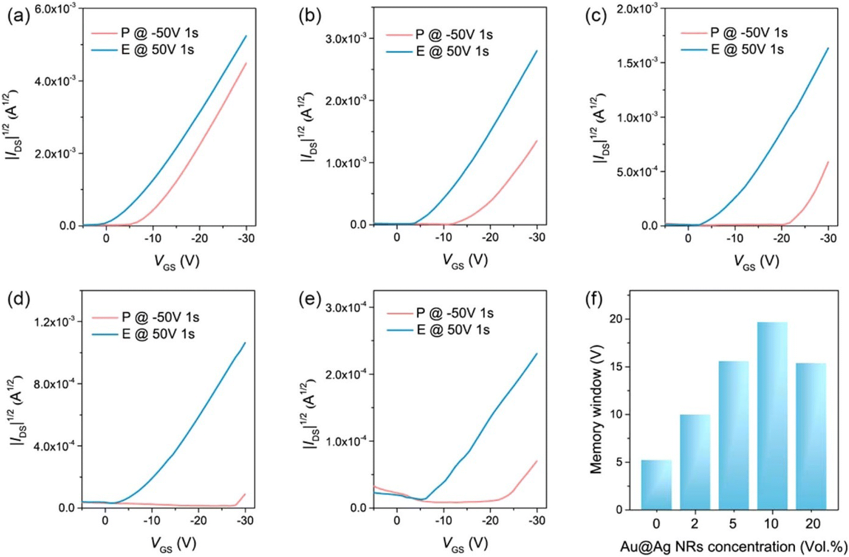 | ||
| Fig. 3 Memory characteristics of (a) PVPy, (b) NRs-2, (c) NRs-5, (d) NRs-10 and (e) NRs-20 memory devices in programmed and erased states. (f) Comparison of memory windows with different concentrations of Au@Ag NRs. Reprinted (adapted) with permission from ref. 77. Copyright 2022 American Chemical Society. | ||
It is noteworthy that the Vth shift of the pristine PVPy floating-gate based memory device is very small owing to the fact that the charge trapping capability of the bulk PVPy is inferior. However, significant Vth shifts are observed in case of the Au@Ag NRs-PVPy based memory devices after the programming operation. The shifting of Vth in the negative direction indicates that the Au@Ag NRs act as the hole trapping elements. Through the application of the reverse bias, the shift of the Vth occurs to the identical initial position suggesting that the holes can be easily trapped or detrapped in the Au@Ag NRs. The memory window (ΔVth) which is defined as the variation of the Vth during the programming and erasing operation gradually enhances from 10 V to 19.7 V with the increase of the doping concentration 2 to 10 vol% in Au@Ag NRs. However, further increase in the concentration of Au@Ag NRs results in a decrease of the memory window, perhaps due to the increased hole conduction among neighboring NRs and reduced charge trapping capacity originating from the severe aggregation of NRs at high concentration. The devices exhibit a data retention time of 104 s and a durability of at least 100 program per erase cycles.
The working mechanism of the Au@Ag NRs based OFET optical memory device is explained in Fig. 4. When light is illuminated on to the top surface of the memory device during the programming process, an enormous number of excitons are generated in the pentacene layer. Pentacene has a high exciton binding energy of ca. 0.5 eV. Excitons produced in pentacene due to light illumination are dissociated by the strong gate-channel electric field. The photogenerated holes are trapped by the Au@Ag NRs resulting in the alternation of Vth shift. Consequently, the increase in the effective charge carriers in the pentacene channel results in a much more positive shift of Vth compared to the Vth shift under the dark programming process. During the light assisted erasing process, the detrapped holes as well as the photoexcited holes are transferred from the Au@Ag NRs back to the pentacene channel layer, inducing a much positive shift of Vth compared to Vth shift under dark erasing process. The phototunable memory effect in the Au@Ag NRs-PVPy floating-gate based OFET optical memory originates from the multimode LSPR effect Au@Ag NRs. As shown in the finite-difference time-domain (FDTD) simulation of the LSPR effect in the Au@Ag NRs-PVPy nanocomposite is shown in Fig. 2(d) and (e), the longitudinal electric field distribution is more pronounced compared to the transverse one. Hence, enhanced light absorption is derived mainly from the longitudinal mode.
 | ||
| Fig. 4 Energy band diagram of OFET optical memory device (a) In the dark while programming, (b) In the dark while erasing, (c) while programming under light irradiation and (d) while erasing under light irradiation. Reprinted (adapted) with permission from ref. 77. Copyright 2022 American Chemical Society. | ||
An analogous work by Wang et al.79 showed that an oriented polystyrene-tethered gold nanorod (AuNR-PS) array structure (Fig. 5(a)) working as a nanostructured floating-gate, was able to tune the absorption features of the active pentacene layer through localized surface plasmon resonance. The authors leveraged the perpendicular oriented AuNR-PS array in a low illumination time of 1 second, as compared to the 3-second duration in random AuNR-PS, shown in Fig. 5(b) and (e). With a data retention duration of 9000 seconds and stability over 50 cycles, it was found that the erased state current in the oriented AuNR-PS was a magnitude lower than the random oriented AuNR-PS (Fig. 5(c), (d) and (f), (g)).
 | ||
| Fig. 5 (a) Schematic illustrations of the perpendicular orientated AuNR@PS array as nano-floating-gate (left) and random AuNR@PS as nano-floating-gate device on the right, (b) programming and erasing characteristics, (c) retention characteristics, and (d) endurance characteristics of the pentacene-based nanostructured floating-gate memory device with perpendicular orientated AuNR@PS array. (e) programming and erasing characteristics, (f) retention characteristics, and (g) endurance characteristics of the pentacene-based device with random aligned AuNR@PS. The current states were measured at VDS = −30 V and VGS = 0 V. Reprinted with permission from ref. 79. Copyright 2023 John Wiley and Sons. | ||
There are other published works that use plasmon nanoparticles in an OFET scheme for memory applications,10,80–88 but they do not exploit plasmons per se. For instance, Chang et al. demonstrated a non-volatile OFET memory device based on poly(9,9-dioctylfluorene-alt-bithiophene) [F8T2] with various ligand-capped AuNP monolayers on the dielectric. It was found that higher AuNP loading on the ligand chain (or using a shorter chain) had a positive impact on the memory window and gave a much improved ratio of programmed to erased state currents (Fig. 6(a) and (b)).86 Oh et al. used a self-assembled monolayer of aptamer conjugated with hexagonal Au nanoparticles (LSPR peak of 525 nm) for charge trapping effects and showed a pronounced hysteresis with the use of Au NPs (Fig. 6(c) and (d)).81 Similarly, Wang and colleagues showed the effects of varying Ag film thickness from 1–10 nm on the transistor performance.82 Liu et al. integrated gate dielectric SiO2 with gold nanoparticles to use as floating-gate for charge storage.83 While we acknowledge that the above articles have shown improvements in device performance with a metal nanoparticle-integrated architecture, we have attempted to explain in depth only those works that have utilized the plasmonic behavior of metal nanoparticles in enhancing the OFET performance and/or functionality.
 | ||
| Fig. 6 (a) Schematic configuration of the OTFTs memory devices on the SAM-modified SiO2 surface using the hybrid materials of F8T2:ligand-capped Au NPs, and optical absorption spectra of the modified-Au NPs on the right, (b) retention times and programmed and erased state currents of SAM-modified and unmodified dielectric (reprinted with permission from ref. 86. Copyright 2013 American Chemical Society), (c) and (d) C–V curves of with and without hexagonal AuNPs respectively showing pronounced hysteresis in (d). Reprinted with permission from ref. 81. Copyright 2013 Applied Physics Letters. | ||
3. OECTs integrated with plasmonic nanoparticles
Due to their low fabrication cost, organic transistors are often used as OFETs and OECTs for biological interfaces and sensors. An OFET is a metal-oxide-semiconductor field-effect transistor (MOSFET) where the active region is an organic semiconductor whereas OECTs have an electrolyte instead of a dielectric layer between the gate and the active region. The channel current and transconductance can be controlled by modifying the materials used for the gate, the active layer and electrolyte with parameters such as concentration, functionalization with a self-assembled monolayer (SAM), immobilization with nanoparticles, and de-doping. OECTs are particularly sensitive in detecting affinity binding events and therefore find use in immunoassays.89 OECTs have the advantage over OFETs for biosensing given OECTs are stable in aqueous solution and work at lower voltages.90,91 Moreover, they have also shown transconductance in the mS range, as reported by Dion Khodagholy et al. in 2013.92With plasmonic nanoparticles introduced in either the gate electrode or immobilized on a SAM, immunosensors and bio-electronic interfaces have demonstrated an improved performance in sensing. In particular, Au NPs have been the plasmonic material of choice because of good compatibility and signal amplification.93 One of two ways in which Au NPs is being used to achieve this – to fabricate the gate electrode by either combining Au NPs with another material or used by themselves, or in the active layer/electrolyte to enhance the conductivity of the channel through improved charge transfer. Based on this, there are three mechanisms that explain the improvement resulting in the performance of OECTs from integrating Au NPs. The first is the local electromagnetic field enhancement when gold is part of the gate electrode. The second is the enhanced charge transfer to the electrolyte when gold nanoparticles are introduced in the electrolyte. The third is improving the conductivity of the active layer through immobilization of Au nanoparticles on a SAM-coated active region. With these configurations, improved performance metrics were achieved.
In 2010, Duck-Jin Kim et al. reported one of the first point-of-care (POC) diagnostic systems based on an OECT-gold nanoparticle integrated immunosensor for the detection of prostate cancer.94 A poly(styrenesulfonate)-doped poly(3,4-ethylenedioxythiophene) PEDOT:PSS channel with 1/4th concentration of ethylene glycol (EG) was formed. EG was introduced to increase the channel conductivity. Au NPs of 10 nm size were deposited on prostate specific antigen-polyclonal antibody (PSA-pAb) with a carboxylated SAM layer on the Au NPs. It was observed that with the use of Au NPs, the channel current could be enhanced resulting in a lower limit of detection (from 100 pg ml−1 to 1 pg ml−1) of the prostate specific antigen/α1-antichymotrypsin (PSA-ACT) complex concentration, as shown in Fig. 7. The presence of gold nanoparticles shifted the absorption peak from 517 nm to 523 nm resulting in a red colored solution caused by the carboxylated SAM layer changing the local refractive index. Together with the enhanced conductivity in the PEDOT:PSS channel, Au NPs on the PSA-pAb, owing to their large effective surface area, improved the electron transfer to the PSA-ACT complex, dramatically increasing the sensitivity.
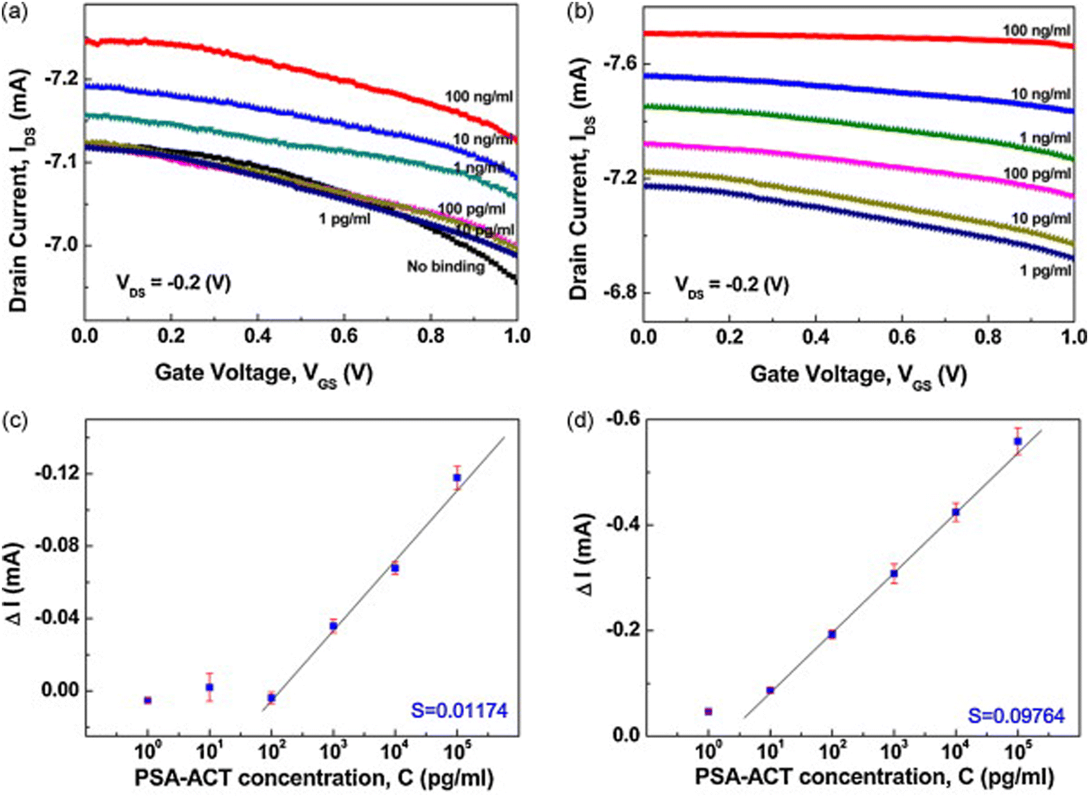 | ||
| Fig. 7 I–V curve of the OECT based immunosensor (a) without AuNP, and (b) with AuNP. (c) and (d) calibration curve without and with AuNPs respectively. Reprinted from ref. 94 with permission from Elsevier. | ||
A similar article was published in 2018 by Jia-An Chou et al. where they reported the dual use of immobilized gold nanoparticles on the thiol-functionalized PEDOT films for both the detection of dopamine using OECTs and as surface enhanced Raman scattering (SERS)-active substrates for p-cresol detection.93 The coating of the thiol-functionalized PEDOT film with Au NPs improved the transfer characteristics and made it possible to detect 37 nM of dopamine, as shown in Fig. 8. The gold nanoparticles increased the conductivity of the thiol-functionalized (PP-SH) layer because of its high specific area, causing less difference between the on and off current. This feature could be useful for the smooth switching of the AuNP-PP-SH OECT. At the same time, the same OECT device provided greater SERS hot spots due to the presence of gold nanoparticles and was able to detect varying levels of p-cresol, although it performed marginally better in the high concentration regime of the p-cresol.
 | ||
| Fig. 8 Output curves of the device with (a) a single layer PEDOT film (P), (b) thiol-functionalized PEDOT film (PP-SH) and without AuNPs, and (c) PP-SH with AuNPs. (d) Transfer curves, (e) Transconductance vs gate voltage, Vg for potential sweep from 0 to 0.8 V and (f) Transconductance vs. Vg for AuNPs@PP-SH OECT, recorded in 1× PBS (pH 7.4) with 1 mM dopamine for different drain voltages and Vg sweep from −0.5 V to 0.6 V. Adapted from ref. 93 under the Creative Commons License. | ||
Au NPs were used in a different way in an organic photoelectrochemical transistor (OPECT)-based DNA sensor, reported by Jiajun Song et al. in 2018.95 The photoelectrochemical gate electrode consisted of cadmium sulfide (CdS) quantum dots (QDs) on an ITO glass substrate, and the target DNA was labeled with gold nanoparticles. Exciton-plasmon interaction (EPI) takes place between the Au plasmons and the CdS excitons. Two mechanisms – the plasmonic analog of Förster-type resonance energy transfer (FRET) and LSPR-induced rise in the spontaneous emission rate of CdS QDs work cooperatively to dissipate excitonic energy and reduce the number of photoelectrons transferred from CdS QDs to the gate electrode. It is important to note that plasmon-induced resonance energy transfer is bidirectional but similar to FRET, depends on the overlap of the emission and absorption spectra of the CdS QDs and Au NPs respectively.96 The measured current depends on the DNA concentration which is the main sensing mechanism in the device.95 As expected for FRET/PIRET and other molecular rulers, the DNA detection limit was highly dependent on the length of the DNA strands and dropped off for longer strands. A detection limit of 1 fM was reached for the single-stranded DNA used in the study demonstrated in Fig. 9. Although the device was primarily used as a sensor, it also worked as an amplifier where increasing the width/length ratio of the channel resulted in a higher drain current.
 | ||
| Fig. 9 (a)–(c) represent channel current versus time for 1 × 10⁻⁶ M, 1 × 10⁻¹⁰ M and 1 × 10⁻¹⁵ M respectively, and (d) ΔI/I versus concentration of target ssDNA, R being the linear regression equation parameter. Reproduced with permission from ref. 95©2018 WILEY-VCH Verlag GmbH & Co. KGaA, Weinheim. | ||
A nanostructured plasmonic gate was also reported by Jayan Thomas et al. in which OECT was used for monitoring brain signals.91 With the use of nanostructured interdigitated electrodes (IDEs) of gold (50 nm) formed by electron beam lithography (EBL), the group has reported that while using a wavelength of light same as the resonant peak, the surface plasmon resonance resulted in highly localized electrons near the surface. This reduced the impedance and could be utilized to improve the sensitivity of the gold IDEs.
4. Plasmon enhanced phototransistors
Organic phototransistors have already demonstrated more sensitive photodetection than high performance silicon photodiodes for specific wavelengths.97 The general configuration of organic phototransistors (OPTs) is the same as OFETs with a substrate, a dielectric layer, an active layer, and three electrodes: a source, a drain, and a gate. As a bias is set across the source and drain electrodes, it creates a channel of accumulated charges between the two electrodes through the active layer. The gate electrode allows for the application of a bias that controls the flow of charge between the source and drain. The dielectric layer acts as a capacitor between the gate and source/drain electrodes. This allows the OPT to act as a switch in the electronics. The difference between an OPT and an OFET is the use of incident light to amplify the signal of the transistor. OPTs work in the light receiving mode of typical transistors, where an incident photon excites carriers in the active layer (typically an organic semiconductor), generating excitons. The bound Frenkel excitons are dissociated into mobile carriers by the strong gate-channel electric field thus resulting in a drain current driven by the bias between the source and drain allows for a higher overall electrical signal in the device. Even while the OPT is in the ‘off-state’, that is at zero gate bias, there is still a small amount of current flowing between the source and drain electrodes, known as the dark-current.There are two working modes of an OPT: the photovoltaic mode and the photoconductive mode. In the photovoltaic mode, the device is in the on-state, meaning the gate voltage is lower than the threshold bias (using a p-type OSC as the active layer), where the threshold bias is the minimum gate-source voltage to begin the operation of the device. As the device is illuminated, the voltage threshold will shift. In photoconductive mode, the OPT is in the off-state and thus the gate voltage is greater than the threshold voltage, and the gate voltage will increase with increasing illumination power.98
The performance factors taken into consideration when determining the effectiveness of the OPT are photoresponsivity, detectivity, and photosensitivity. Photoresponsivity (R) is the ratio of the photocurrent and the incident power of illumination. Detectivity (D*) is a combination of bandwidth, noise equivalent power, and area. The detectivity allows for a quantitative comparison between the sensitivity of different OPTs, with higher detectivity indicating higher performance. Finally, the photosensitivity (P) is the ratio of illuminated energy with the dark photocurrent. The carriers generated from the absorbed light in the active layer can be further enhanced by the introduction of plasmonic nanoparticles into the fabrication process into either the surface-active layer or the active-insulating layer, as shown in Fig. 10(a) and (b), respectively. These could be in the form of Ag NPs,99,100 Au NPs101,102 and Au nanorods.103
 | ||
| Fig. 10 Example configurations for organic phototransistors with the addition of gold nanoparticles. (a) The gold nanoparticles are deposited on the insulating layer. The active layer is then deposited on the nanoparticle layer. Reprinted from ref. 102, with permission from IOP Publishing Ltd. (on behalf of Japan Society of Applied Physics). (b) The nanoparticles are deposited on the active layer of the organic phototransistor with direct contact to incoming light. Reprinted (adapted) with permission from ref. 101. Copyright 2018 American Chemical Society. (c) Schematic of working properties of plasmonic enhancement of organic phototransistors. Light is incident onto a nanoparticle located on the active layer. The enhancement of the local field from the nanoparticle increases exciton dissociation, causes hot electron effects, and induces carrier transitions. Reprinted (adapted) with permission from ref. 101. Copyright 2018 American Chemical Society. | ||
The working mechanism of the enhancement from the LSPR phenomenon is schematically shown in Fig. 10(c). The gold NPs enhance the absorption of the active layer thanks to the LSPR coupling with the molecules in the active layer, causing higher dissociation due to a higher built-in field.101,104 Also, hot electron effects add more carriers to the total number of charges collected by transport channels.101,105 Lastly, there can be an energy transfer due to dipole–dipole coupling and near-field enhancement inducing carrier transitions.101,106 The measured improvement in the photoresponsivity due to the addition of NPs under different measured conditions is shown in Fig. 11. There is a notable increase in R in the OPT with Ag NPs deposited on the insulating layer at visible wavelengths of incident light (Fig. 11(a)).99 This increase is related to the penetration depth of 5,5′′-bis(naphth-2-yl)-2,2′:5′,2′′-terthiophene (NaT3) (57 nm at light wavelength of 360 nm; 540 nm at light wavelength of 475 nm). Since the Ag NPs are deposited between the active layer and the insulating SiO2 layer, enhancement of the photoresponsivity will depend on the penetration depth of the active material. Thus, at low penetration depths the LSPR excitation is lower, and at higher penetration depths the photoresponsivity is enhanced by the LSPR excitation. An increase in R is also observed in the OPT with Au NPs deposited on the surface of the OSC across different gate-source voltage values compared to the same OPT without NPs (Fig. 11(b)).102 The largest increase of R from the NP-OPT and the reference OPT occurs at positive gate-source biases.
 | ||
Fig. 11 Comparing the photoresponsivity (R) of organic phototransistors (OPTs) with and without the addition of metal nanoparticles (NPs). (a) R of an OPT with Ag NPs and NaT3 as the active SC. The R is increased four-fold at wavelengths from 350 nm to 400 nm. Adapted from ref. 99, with permission from Elsevier. (b) R of an OPT with and without Au NPs and P3HT as the active layer. The R of the NP-OPT is higher than the R of a reference OPT for all values of a gate voltage. Adapted from ref. 102©The Japan Society of Applied Physics. Reproduced with permission from IOP Publishing Ltd. All rights reserved. (c) R value comparison of an OPT with Au NPs and without (pristine). The active layer is CuPc. The R value for the plasmonic device increases to 23![[thin space (1/6-em)]](https://www.rsc.org/images/entities/char_2009.gif) 359 A W−1 at low fluences, indicating a higher R range. Reprinted (adapted) with permission from ref. 101. Copyright 2018 American Chemical Society. 359 A W−1 at low fluences, indicating a higher R range. Reprinted (adapted) with permission from ref. 101. Copyright 2018 American Chemical Society. | ||
Finally, an increase in R is also observed in the OPT with Au NPs deposited on the surface of the OSC over different incident light intensities (Fig. 11(c)).101 It was observed that the pristine (no NP device) had an inadequate response below a certain incident power. In contrast, the R of the NP-OPT continued to increase at very low powers, allowing for the OPT to be used in low-light conditions. The photoresponsivity range of the device is thus increased 4-fold with the inclusion of Au NPs. One final observation comes from the interesting behavior of the photosensitivity shown in Fig. 11(b). The plasmonic OPT has a lower P value than the OPT without Au NPs until a crossover point at a gate-source bias of approximately −17 V. Nevertheless, the lower value of P in the plasmonic OPV is attributed to a leakage current.
Detection of circularly polarized light (CPL) has recently attracted a lot of research attention for applications in spintronics, LiDAR, bioimaging, magnetic recording, next generation optical communications, etc. For optimal use of CPL, a suitable detection technology of the chiral polarized states of CPL namely right CPL and left CPL, is needed. Polarizers and filters are traditionally used for CPL detection but reduce the intensity of the illumination resulting in low efficiency. Chiral plasmonic materials with a high chiroptical activity are a potential solution since they offer a high selectivity towards the polarized CPL states. Chiral plasmonic photodetectors generate an amplified response to CPL by modifying the local electromagnetic environment in the light–matter interaction zone such that even materials with a low or non-existent intrinsic CPL response produce a dissymmetric current. The detection mechanism relies on the CPL-selective enhancement of the local electromagnetic field in chiral plasmonic nanostructures such as Z-shaped Ag NPs and fan-like Au NP arrays which in turn influences the efficiency of injection of hot electrons over a Schottky barrier of the plasmonic metal with a nearby semiconductor. Numerical research by Kim, H. et al.107 has shown that a circular-polarization-sensitive organic photodetector based on a chiral plasmonic nanostructure could achieve high efficiency of 23.8% as well as high dissymmetry factor of absorption value of 1.6.
Independent works by Namgung et al.108 and Han et al.109 have shown that phototransistors based on chiral plasmonic nanoparticles in a hot electron transistor and chiral diketopyrrolopyrrole (DPP)-based conjugated polymers active layers respectively, are candidates for effective CPL detection. With the use of a chiral gold nanoparticle array over InGaZnO, Namgung et al.108 were able to achieve a photoresponsivity of 1 A W−1 that was also able to differentiate between the right CPL and left CPL owing to the different hot electron injection efficiency in each case. The work of Han et al.109 involved fabrication of an organic phototransistor based on chiral DPP-based donor–acceptor type π-conjugated polymers. The synthesized polymer had an exceeding charge transport properties and was able to achieve sensing of near-infrared CPL (920 nm) with a photoresponsivity of 26 A W−1. The results reported in both the aforementioned cases surpass previously reported performance and it is conceivable that integrating plasmons with organic molecules towards CPL detection could result in even better performance and efficiency, as shown by Kim, H. et al.107 in their modelling experiment.
5. Plasmon-integrated OLETs
Organic light emitting transistors (OLETs) are a unique class of devices that employ the intrinsic characteristics of switching/amplification and light-emission of OFETs and OLEDs respectively. The first OLET publication was reported as early as 2003110 but the comparatively slower progress in organic electronics did not allow much research and development in this device area. Modern flexible displays that employ OLEDs need OFET driving circuitry to turn on/off the individual pixels in the display. OLETs offer the advantage in this regard since they have inbuilt FET driving circuitry which saves space and meets power requirements. An in-plane flow of charge carriers owing to the planar architecture of OLETs with higher mobilities of electrons and holes and enhanced electroluminescence quantum efficiency are advantages in OLETs over OLEDs.111 Capelli, R. et al. (2010) also reported a p-channel/emitter/n-channel trilayer OLET with reduced exciton quenching and photon loss processes whose efficiency was at least 100 times better than equivalent OLEDs and >10 times than other OLETs.112 Unlike OFETs, OLETs need to have electrons and holes both present in the active layer to recombine and emit light. This could be done in two ways- (i) Unipolar OLETs-supplying only holes/electrons in the self-doped active organic semiconductor (OSC) region and allowing them to recombine with the opposite carrier given by the OSC, or (ii) Ambipolar OLETs-supplying both electrons and holes from drain and source electrodes or vice-versa. The first scenario is simpler where a certain p-type OSC recombines with the electrons injected from the metal electrode and radiative recombination takes place. The second case involves finding a suitable OSC whose LUMO and HOMO match with the source and drain electrodes’ work function thus enabling efficient injection of both holes and electrons to recombine in the active layer. Such OSCs are difficult to synthesize and therefore, certain indirect routes that could result in higher electroluminescence in ambipolar OLETs, could be adopted. One way to achieve this is to tune the recombination zone by separating high charge density and exciton generation regions, thus minimizing exciton quenching in OLETs.113,114 Integrating plasmonic NPs into OLETs serves multiple functions. On one hand, the interaction between electrically generated excitons and surface plasmons can be tuned from the weak coupling regime to the strong coupling regime (i.e. plexcitons) using a suitable architecture and applied bias to maximize the local electroluminescence efficiency. On the other hand, the directionality and outcoupling efficiency of emitted light in an OLET can be improved by integrating plasmonic NPs into the active layer.Moving beyond their inherent task of light emission, OLETs have also been reported to function as optical sensors in conjunction with organic photodetector (OPD) and plasmonic layer. In their journal article in 2021, M. Prosa et al.115 reported a unique device that combined the functions of an OLET, OPD and nanoplasmonic grating (NPG) (Fig. 12(a)–(d)), which was demonstrated to sense an optical signal and produce an output response to it.
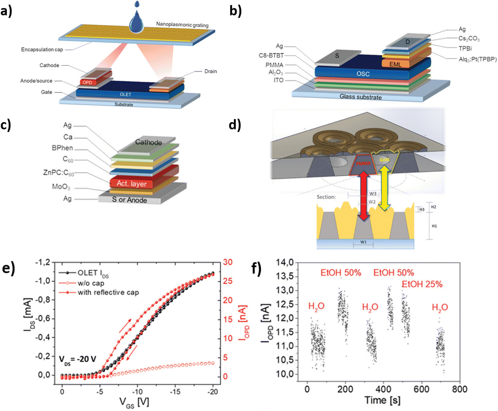 | ||
| Fig. 12 (a) Overall scheme of the optoplasmonic sensing system. (b) OLET part of the device with its individual layers. (c) OPD part. (d) The nanoplasmonic grating with PMMA pillars embedded in a thick Au layer. (e) OLET drain-to-source current and OPD output current with and without the NPG reflective layer. (f) Variation of OPD current over time with the change in the surrounding medium. Adapted with permission from ref. 115. Copyright 2018 Advanced Functional Materials. | ||
The NPG consists of poly(methyl methacrylate) (PMMA) pillars embedded in the gold layer and reflects light up to 98% in the broad near-infrared (NIR) wavelength range, when they are illuminated at an angle at their resonance wavelength. The organic semiconductor chosen was 2,7-dioctyl(1)benzothieno(3,2-b)(1)benzothiophene (C8-BTBT) which is a p-type material. It is worth mentioning that this device belongs to the class of unipolar OLET devices. The emissive layer was a blend of PtII–tetraphenyltetrabenzoporphyrin (Pt(tpbp)) and tris(8-hydroxyquinoline), (Alq3) with an emission wavelength of 770 nm. Silver was used as source and drain electrodes, and the source also acted as the anode of the OPD. The OLET, OPD and NPG were spectrally matched and since the OLET emissive layer and NPG have responses in NIR around 770 nm, zinc phthalocyanine (ZnPc) with fullerene-C60 doping was employed as material for OPD because of its absorption in NIR. The NPG is fabricated on a transparent glass substrate to allow the smooth passage of light from the Ag layer (at drain) during the emission from the OLET part of the device. The OPD absorbs the reflected light caused from the angular excitation of the surface plasmons in the NPG. Consequently, a small electric signal is produced by the photodetector in response to the incident light on it.
As shown in the overall response of the sensing system in Fig. 12(e), the output current is negligible when there is no Au layer (NPG reflective cap) present on the top of the encapsulating glass substrate. This confirms the reflective action is taking place from the NPG layer. The other factor that affects the OPD response is the change in the surrounding medium of the NPG layer (Fig. 12(f)). To realize this, the authors first used 100% water solution over an adhesive silicon sheet on top of the NPG layer as the reference, followed by a mixture of water and ethanol. For the latter case, OPD current increased to 12.3 ± 0.3 nA when 50% ethanol was used compared to 11.1 ± 0.3 nA for just ultrapure water. Further, using 100% water over NPG caused a threefold reduction in current with respect to full reflective coating. Further improvements were observed in signal to noise ratio with the use of interdigitated chip (two source/OPDs on either side of the drain), thereby doubling the light collected.
Integration of surface plasmons in OLETs have also shown improvement in electroluminescence yields and directionality of emission. In their work, Zakharko et al.116 reported an enhancement in infrared (1100 nm) electroluminescence by combining a high mobility and balanced polymeric semiconductor layer (diketopyrrolopyrrole copolymer, DPPT-BT, 15 nm thick) with 20 nm gold nanorods in a light-emitting field-effect transistor (LEFET) planar architecture, that allowed vertical near-field coupling of the tunable exciton source to the localized surface plasmons of gold nanorods. The presence of gold nanorods in the active region leveraged the Purcell effect to increase the radiative decay rate of excitons (by increasing the photonic density of states and suppressing non-radiative decay, and hence photonic efficiency).117 When the recombination zone in the LEFET is positioned close to the gold nanorods, the localized surface plasmons (LSP) supported by the nanorods couple with the excitons, leading to enhanced light emission. This coupling is controlled by adjusting the applied drain and gate voltages, which moves the recombination zone closer to or further from the nanorods, effectively turning the enhancement on or off. The high local field concentration at the tips of the nanorods facilitates this near-field coupling, resulting in a significant increase in electroluminescence intensity. The authors also demonstrated that a 130-fold increase in the final quantum yield could be achieved when the dipoles were 1 nm from the longer side of the nanorods compared to 260 times lower quantum efficiency for dipoles perpendicular to the nanorod length at the same distance, owing to metal quenching.116
Working on the same principle, Zakharko et al.118 further worked on to limit the intrinsic losses associated with the plasmonic metal and discussed a mechanism for enhanced and directional luminescence in LEFETs by introducing surface lattice resonances (SLRs). Using the same polymeric layer DPPT-BT (40 nm thick), the LEFET device was embedded with periodic gold nanodisks (AuNDs, 25 nm high, over 20 × 500 μm2 area) in the semiconducting channel. The Purcell effect enhanced light emission while the presence of SLRs along with a non-metallic gate electrode (200 nm PEDOT:PSS) allowed non-destructive interference with the AuNDs. Consequently, a high and directional emission was observed through angle- and energy-resolved electro- and photoluminescence. The range of light emission could be controlled by varying semiconducting layers, applied voltages and geometry of the plasmonic nanostructures.118
6. Gated terahertz photodetectors exploiting graphene plasmons
The terahertz (THz) band of the electromagnetic spectrum (roughly 10–300 cm−1) is gaining increasing importance for applications such as chemical fingerprinting, long-distance space communication, cross-barrier vision, label-free non-invasive biomedical imaging devices, food and crop inspection, etc.119–121 These devices rely on the ability of terahertz radiation to (i) penetrate non-transparent objects for perspective imaging (ii) detect vibrational resonances of molecules and (iii) carry encoded information over long distances without loss. For active solid-state terahertz devices and integrated circuits, it is important to be able to squeeze the energy and information content of THz photons into much smaller volumes and then manipulate them in a controllable manner. In the visible and near-infrared (NIR) spectral ranges, this is done by coupling light to plasmons to the interfaces of low loss metals such as Ag and Au with dielectrics, creating surface plasmon polaritons that can carry the energy and information content of light for tens of micrometers while requiring a much smaller mode volume. At THz frequencies, noble metals such as Ag and Au provide weak confinement of THz photons and exhibit high ohmic losses, rendering them unsuitable for active THz plasmonic devices such as generators, modulators, splitters and detectors. On the other hand, graphene which is a two-dimensional atomically thick sheet of sp2 hybridized carbon atoms, is capable of confining THz fields into volumes that are a million times smaller than free space.122 Furthermore, the carrier density and band gap of graphene in an FET channel can be modulated using a gate bias.While diodes are well-known rectifying devices, synchronous FETs are also used to rectify AC fields. Terahertz radiation can be considered as an ultra-high frequency AC field whose rectification by FETs requires an extraordinarily high carrier mobility (to keep pace with the rapid spatiotemporal changes in field amplitude) such as exhibited by graphene. Shur and Dyakonov pointed out in 1996123 that the FET channel consists of a two-dimensional electron gas (2DEG) which allows plasma waves with a dispersion relation ω = sk to propagate in the channel where ω is the angular frequency, k is the wave vector and s is the wave velocity. s is given by  where e is the elementary charge, m* is the carrier effective mass and U is the gate-to-channel voltage swing. A graphene field-effect transistor (GFET) with graphene plasmons as waveguide was used to fabricate reconfigurable THz nanodevices by Chen et al., aimed at a variety of applications in sensing, biomedical and wireless communication.124 Hu and others demonstrated that using ion gel as dielectric in a top-gated graphene plasmon FET intended for terahertz applications, resulted in broadly tunable graphene plasmons (plasmonic shift of ∼1270 cm−1) while still employing a relatively low voltage modulation.125 A similar work by Bandurin and coworkers reported a resonant THz photodetector consisting of an antenna coupled graphene MOSFET whose channel acted as a Fabry–Perot resonator for graphene plasmons (Fig. 13).126 The incident free space THz radiation was compressed into highly confined graphene plasmons and the resulting AC potential was rectified using the graphene FET (Fig. 14). High mobility charge carriers and plasmon confinement were achieved using bilayer graphene nanosheets encapsulated between hexagonal boron nitride (h-BN) sheets to minimize interface defects and scattering.126 Likewise, the resonance frequency of the transistor channel could be tuned by varying the channel length and carrier density.
 | ||
| Fig. 13 (a) Schematic illustration of the FET configuration used for resonant THz detection exploiting plasmons in a bilayer graphene (BLG) channel encapsulated between two boron nitride layers (b), (c) Three-dimensional rendering and top-view photograph of the lens and antenna-coupled THz detection FET architecture consisting of a hemispherical silicon lens focusing incident free space terahertz radiation on to a broadband bow-tie antenna which also served as the gate and source electrodes of the BLG FET and (d) Temperature-dependent conductance of the BLG FET with inset showing a zoomed-in top view of the device with a top-gate over a channel with source (upper) and drain (lower) electrodes. Reprinted from ref. 126 under the terms of a Creative Commons license. | ||
 | ||
| Fig. 14 Responsivity as a function of temperature and bias at 0.13 THz (a) and as a function of applied bias at 10 K and 2 THz (b) of the resonant terahertz photodetector exploiting graphene plasmons whose structure is shown in Fig. 13. Reprinted from ref. 126 under the terms of a Creative Commons license. | ||
7. Conclusions and outlook
Optoelectronics technology at the current time is dominated by inorganic semiconductor active layers with CMOSFETs being the device of choice in most applications relating to switching and amplification. However, organic semiconductor-based field-effect transistors occupy specific niches related to flexible and printed electronics, photodetection, light emission, optical non-volatile memories, electrochemical sensors, etc. where they provide either improved performance or additional functionality over that afforded by Si CMOS technology. These advantages originate in the higher oscillator strength, direct bandgap, environmental sensitivity, ion permeability and electrochemical recyclability of organic semiconductors compared to silicon-based FETs which are incapable of strongly absorbing or emitting light due to the indirect bandgap of Si and the tendency of Si to form a native oxide in aqueous electrolytes. The integration of plasmons emphasizes the inherent advantages of organic semiconductors by further enhancing light-matter interactions and improving charge transfer processes.Organic field effect transistor (OFET) sensors exhibit a significantly higher sensitivity than traditional biosensors due to the signal gain/amplification function intrinsic to all FETs. Consequently, any further enhancements in the performance of OFETs through the incorporation of plasmons would naturally place such OFET-based sensors at the cutting edge of detection limits for photons, biomolecules and other analytes of interest. A second factor that makes it interesting to combine coinage metal nanoparticles with organic semiconductors is the strong light–matter interaction exhibited by both surface plasmons and Frenkel excitons, thus stimulating devices and applications where the excitons and plasmon quasiparticles are coupled to each other as plexcitons. A third factor is that both gold nanoparticles and organic semiconductors are compatible with inexpensive and facile solution processing, which renders plasmon-enhanced OFETs particularly attractive for use in bio-electronic interfaces and wearable electronics, despite their lower mobility compared to inorganic transistors.
An OFET optical memory with a pentacene thin film channel and a floating-gate architecture consisting of Au@Ag core–shell NRs-PVPy nanocomposite was reviewed. The application of a programming gate voltage of −50 V drives holes to the floating gate, charging it and thus shifting the threshold voltage. A deprogramming/erase voltage of +50 V restores the threshold voltage to its original value. A tunable memory window is achieved by varying the size of the Au core or the thickness of Ag shell as well as the concentration of Au@Ag NRs in the floating-gate. Moreover, the memory characteristics of the memory device are phototunable due to localized surface plasmon resonance of the Au@Ag NRs resulting in light sensing and data storage functionalities. A similar pentacene-based active layer with gold nanorods showed phototunable absorption features due to Au nanorod-induced plasmonic enhancement. Plasmon-enhanced organic memory devices are interesting for low-cost applications where a tunable memory window is desired but further improvements are needed to lower the absolute value of the programming and erase voltages employed. The incorporation of plasmonic nanoparticles into the channel and/or gate electrode of OECTs has led to significant increases in the sensitivity of detection of biomarkers, nucleic acids and metabolites arising from the gold-mediated enhancement of electron transfer to electrolyte species. In organic photoelectrochemical transistors (OPECTs), exciton-plasmon interactions further contribute to the improvement of sensor performance.
The incorporation of plasmonic nanoparticles in the channel of organic phototransistors (OPTs) expands the dynamic range of operation of the device over several orders of magnitude. The improvements to the photoresponsivity of OPTs using Au and Ag NPs are apparent for varying light wavelengths, for varying gate-source bias, and for all values of the incident power of the light. The non-negligible and even increasing signal at very low optical power give rise to new applications of plasmon coupled OPTs for low-light applications. OPTs integrating chiral plasmonic NPs enable detection of right- and left-circular polarized light by generating a dissymmetric current. The tunability of device parameters based on the size of the NP could also lead to OPTs for not merely low-light applications but applications outside of the visible spectrum – in the deep ultraviolet and near-infrared for instance. A plasmon-enhanced OLET sensor that allowed for fabrication of a cost-effective device where light emission, reflection and detection take place on a single chip, was reviewed. An OLET consisting of a diketopyrrolopyrrole conjugated polymer channel integrated with gold nanorods (Au NRs) allowed vertical near-field coupling of the excitons with tunable characteristics that were electrically generated in the conjugated polymer to the Au NR plasmons, and the strong Purcell effect resulting from this architecture improved local electroluminescence yields as well as the directionality of emission and the light outcoupling efficiency. The terahertz frequency range is the least mature in terms of mass market applications. One of the challenges in dealing with THz signals is the difficulty in detecting them and amplifying them on-chip. However, graphene plasmons allow unprecedented confinement of THz electric fields and antenna-coupled graphene FETs have been demonstrated to rectify THz signals. Further advances in OFET technology for detecting and amplifying THz signals can be expected using graphene-based active layers as well as high mobility organic–inorganic hybrid channels.
Author contributions
The manuscript was written through contributions of all authors. All authors have given approval to the final version of the manuscript.Data availability
No primary research results, software or code have been included and no new data were generated or analysed as part of this review.Conflicts of interest
The authors do not have any conflicts of interest to report.Acknowledgements
We thank the Natural Sciences and Engineering Research Council of Canada (NSERC) Discovery grants program, the Resilient and Clean Energy Systems Initiative (RCESI) funded by the Government of Alberta Major Innovation Fund, and the Alberta Innovates Advance Program for research funding. MMR acknowledges scholarship funding from Alberta Innovates.References
- G. Chansin, LCD Fights Back Against OLED With MiniLED Backlight Technology, Inf. Disp., 2021, 37(2), 49–51 Search PubMed.
- S. Asnani, M. G. Canu, L. Farinetti and B. Montrucchio, On producing energy-efficient and contrast-enhanced images for OLED-based mobile devices, Pervasive Mob. Comput., 2021, 75, 101384 CrossRef.
- B. Choi, Development of next generation emitting materials for OLED display (Conference Presentation), SPIE, 2022, vol. 12208 Search PubMed.
- E. Kim, J. Kwon, C. Kim, T.-S. Kim, K. C. Choi and S. Yoo, Design of ultrathin OLEDs having oxide-based transparent electrodes and encapsulation with sub-mm bending radius, Org. Electron., 2020, 82, 105704 CrossRef CAS.
- S. Lee, Y. Chen, J. Kim and J. Jang, Vertically integrated, double stack oxide TFT layers for high-resolution AMOLED backplane, J. Soc. Inf. Disp., 2020, 28(6), 469–475 CrossRef CAS.
- Y. Su, D. Geng, Q. Chen, H. Ji, M. Li, G. Shang, L. Liu, X. Duan, X. Chuai, S. Huang, N. Lu and L. Li, Novel TFT-Based emission driver in high performance AMOLED display applications, Org. Electron., 2021, 93, 106160 CrossRef CAS.
- J. Her, W. K. Min, C. S. Shin, H. Jeong, J. K. Park, H. J. Kim and A. New Pixel, Circuit With Selectively Synchronized Dual-Gated IGZTO TFTs for AMOLED Displays, IEEE Trans. Electron Devices, 2022, 69(10), 5568–5573 CAS.
- H. Yu, X. Zhao, M. Tan, B. Wang, M. Zhang, X. Wang, S. Guo, Y. Tong, Q. Tang and Y. Liu, Ultraflexible and Ultrasensitive Near-Infrared Organic Phototransistors for Hemispherical Biomimetic Eyes, Adv. Funct. Mater., 2022, 32(48), 2206765 CrossRef CAS.
- Y.-C. Lin, W.-C. Yang, Y.-C. Chiang and W.-C. Chen, Recent Advances in Organic Phototransistors: Nonvolatile Memory, Artificial Synapses, and Photodetectors, Small Sci., 2022, 2(4), 2100109 CrossRef CAS.
- A.-C. Chang, Y.-C. Lin, H.-C. Yen, W.-C. Yang, Y.-F. Yang and W.-C. Chen, Unraveling the Singlet Fission Effects on Charge Modulations of Organic Phototransistor Memory Devices, ACS Appl. Electron. Mater., 2022, 4(3), 1266–1276 CrossRef CAS.
- N. Chaulagain, K. M. Alam, P. Kumar, A. E. Kobryn, S. Gusarov and K. Shankar, Zinc phthalocyanine conjugated cellulose nanocrystals for memory device applications, Nanotechnology, 2021, 33(5), 055703 CrossRef.
- H. Song, Y. J. Song, J. Hong, K. S. Kang, S. Yu, H.-E. Cho, J.-H. Kim and S.-M. Lee, Water stable and matrix addressable OLED fiber textiles for wearable displays with large emission area. npj Flexible, Electronics, 2022, 6(1), 66 CAS.
- S. Choi, Y. Jeon, J. H. Kwon, C. Ihm, S. Y. Kim and K. C. Choi, Wearable Photomedicine for Neonatal Jaundice Treatment Using Blue Organic Light-Emitting Diodes (OLEDs): Toward Textile-Based Wearable Phototherapeutics. Advanced, Science, 2022, 9(35), 2204622 CAS.
- D. Khodagholy, T. Doublet, P. Quilichini, M. Gurfinkel, P. Leleux, A. Ghestem, E. Ismailova, T. Hervé, S. Sanaur, C. Bernard and G. G. Malliaras, In vivo recordings of brain activity using organic transistors, Nat. Commun., 2013, 4(1), 1575 CrossRef PubMed.
- D. Khodagholy, J. N. Gelinas, T. Thesen, W. Doyle, O. Devinsky, G. G. Malliaras and G. Buzsáki, NeuroGrid: recording action potentials from the surface of the brain, Nat. Neurosci., 2015, 18(2), 310–315 CrossRef CAS PubMed.
- V. Benfenati, S. Toffanin, S. Bonetti, G. Turatti, A. Pistone, M. Chiappalone, A. Sagnella, A. Stefani, G. Generali, G. Ruani, D. Saguatti, R. Zamboni and M. Muccini, A transparent organic transistor structure for bidirectional stimulation and recording of primary neurons, Nat. Mater., 2013, 12(7), 672–680 CrossRef CAS.
- J. McGinness, P. Corry and P. Proctor, Amorphous Semiconductor Switching in Melanins, Science, 1974, 183(4127), 853–855 CrossRef CAS PubMed.
- H. Shirakawa, E. J. Louis, A. G. MacDiarmid, C. K. Chiang and A. J. Heeger, Synthesis of electrically conducting organic polymers: halogen derivatives of polyacetylene, (CH), J. Chem. Soc., Chem. Commun., 1977,(16), 578–580 RSC.
- A. Tsumura, H. Koezuka and T. Ando, Macromolecular electronic device: Field-effect transistor with a polythiophene thin film, Appl. Phys. Lett., 1986, 49(18), 1210–1212 Search PubMed.
- H. Sirringhaus, 25th Anniversary Article: Organic Field-Effect Transistors: The Path Beyond Amorphous Silicon, Adv. Mater., 2014, 26(9), 1319–1335 CrossRef CAS PubMed.
- S.-J. Wang, M. Sawatzki, G. Darbandy, F. Talnack, J. Vahland, M. Malfois, A. Kloes, S. Mannsfeld, H. Kleemann and K. Leo, Organic bipolar transistors, Nature, 2022, 606(7915), 700–705 Search PubMed.
- K. Shankar and T. N. Jackson, Morphology and electrical transport in pentacene films on silylated oxide surfaces, J. Mater. Res., 2004, 19(7), 2003–2007 CrossRef CAS.
- A. K. Chauhan, P. Jha, D. K. Aswal and J. V. Yakhmi, Organic Devices: Fabrication, Applications, and Challenges, J. Electron. Mater., 2022, 51(2), 447–485 CrossRef CAS.
- X. B. Ren, Z. J. Lu, X. J. Zhang, S. Grigorian, W. Deng and J. S. Jie, Low-Voltage Organic Field-Effect Transistors: Challenges, Progress, and Prospects, ACS Mater. Lett., 2022, 4(8), 1531–1546 Search PubMed.
- A. Nawaz, L. Merces, L. M. M. Ferro, P. Sonar and C. C. B. Bufon, Impact of Planar and Vertical Organic Field-Effect Transistors on Flexible Electronics, Adv. Mater., 2023, 50 Search PubMed.
- A. Mohammadpour, B. D. Wiltshire, S. Farsinezhad, Y. Zhang, A. M. Askar, R. Kisslinger, W. T. Delgado, G. He, P. Kar, E. Rivard and K. Shankar, Charge transport, doping and luminescence in solution-processed, phosphorescent, air-stable tellurophene thin films, Org. Electron., 2016, 39, 153–162 CrossRef CAS.
- J. M. Ball, R. K. M. Bouwer, F. B. Kooistra, J. M. Frost, Y. Qi, E. B. Domingo, J. Smith, D. M. de Leeuw, J. C. Hummelen, J. Nelson, A. Kahn, N. Stingelin, D. D. C. Bradley and T. D. Anthopoulos, Soluble fullerene derivatives: The effect of electronic structure on transistor performance and air stability, J. Appl. Phys., 2011, 110(1), 014506 CrossRef.
- A. D. Scaccabarozzi, J. I. Basham, L. Yu, P. Westacott, W. Zhang, A. Amassian, I. McCulloch, M. Caironi, D. J. Gundlach and N. Stingelin, High-density polyethylene—an inert additive with stabilizing effects on organic field-effect transistors, J. Mater. Chem. C, 2020, 8(43), 15406–15415 RSC.
- M. Makala, M. Barłóg, D. Dremann, S. Attar, E. G. Fernández, M. Al-Hashimi and O. D. Jurchescu, High-performance n-type polymer field-effect transistors with exceptional stability, J. Mater. Chem. C, 2024, 12, 17089–17098 Search PubMed.
- S. A. Maier and S. A. Maier, Surface plasmon polaritons at metal/insulator interfaces, Nanoplasmonics:Fundam. Appl., 2007, 21–37 Search PubMed.
- M. A. García, Surface plasmons in metallic nanoparticles: fundamentals and applications, J. Phys. D: Appl. Phys., 2011, 44(28), 283001 CrossRef.
- A. P. Manuel and K. Shankar, Hot Electrons in TiO2-Noble Metal Nano-Heterojunctions: Fundamental Science and Applications in Photocatalysis, Nanomaterials, 2021, 11(5), 1249 CrossRef CAS PubMed.
- X. Xu, D. Aggarwal and K. Shankar, Instantaneous Property Prediction and Inverse Design of Plasmonic Nanostructures Using Machine Learning: Current Applications and Future Directions, Nanomaterials, 2022, 12(4), 633 Search PubMed.
- L. M. Liz-Marzán, Tailoring Surface Plasmons through the Morphology and Assembly of Metal Nanoparticles, Langmuir, 2006, 22(1), 32–41 CrossRef.
- M. Li, S. K. Cushing and N. Wu, Plasmon-enhanced optical sensors: a review, Analyst, 2015, 140(2), 386–406 RSC.
- J. A. Schuller, E. S. Barnard, W. Cai, Y. C. Jun, J. S. White and M. L. Brongersma, Plasmonics for extreme light concentration and manipulation, Nat. Mater., 2010, 9(3), 193–204 CrossRef CAS.
- A. P. Manuel, A. Kirkey, N. Mahdi and K. Shankar, Plexcitonics – fundamental principles and optoelectronic applications, J. Mater. Chem. C, 2019, 7(7), 1821–1853 Search PubMed.
- H. Rajashekhar; N. Kumar; A. P. Manuel; M. Supur; R. L. McCreery and K. Shankar In Raman Thermometry For Sensing Of Hot Carriers In Gold Nanoparticle-Based Bimetallic Photocatalysts, 2022 IEEE Sensors, 30 Oct.-2 Nov. 2022; 2022; pp 1-3.
- X. Qin, W. Y. Sun, Z. H. Zhou, P. Y. Fu, H. Li and Y. Li, Waveguide effective plasmonics with structure dispersion, Nanophotonics, 2022, 11(9), 1659–1676 CrossRef CAS.
- A. Kumari, V. Vyas and S. Kumar, Synthesis, characterization, and applications of gold nanoparticles in development of plasmonic optical fiber-based sensors, Nanotechnology, 2023, 34(4), 16 Search PubMed.
- R. Adhikari, Z. Sbeah, D. Chauhan, S. H. Chang and R. P. Dwivedi, A Voyage from Plasmonic to Hybrid Waveguide Refractive Index Sensors Based on Wavelength Interrogation Technique: a Review, Braz. J. Phys., 2022, 52(3), 28 CrossRef.
- J. M. Li, J. Y. Liu, Z. R. Guo, Z. Y. Chang and Y. Guo, Engineering Plasmonic Environments for 2D Materials and 2D-Based Photodetectors, Molecules, 2022, 27(9), 21 Search PubMed.
- J. C. Zhang, Y. W. Wang, D. Li, Y. H. Sun and L. Jiang, Engineering Surface Plasmons in Metal/Nonmetal Structures for Highly Desirable Plasmonic Photodetectors, ACS Mater. Lett., 2022, 4(2), 343–355 Search PubMed.
- A. Ali, F. El-Mellouhi, A. Mitra and B. Aissa, Research Progress of Plasmonic Nanostructure-Enhanced Photovoltaic Solar Cells, Nanomaterials, 2022, 12(5), 37 Search PubMed.
- S. Liu, Y. Sun, L. Chen, Q. Zhang, X. Li and J. Shuai, A review on plasmonic nanostructures for efficiency enhancement of organic solar cells, Mater. Today Phys., 2022, 24, 17 Search PubMed.
- P. Mandal, Application of Plasmonics in Solar Cell Efficiency Improvement: a Brief Review on Recent Progress, Plasmonics, 2022, 17(3), 1247–1267 Search PubMed.
- E. Vahidzadeh, S. Zeng, A. P. Manuel, S. Riddell, P. Kumar, K. M. Alam and K. Shankar, Asymmetric Multipole Plasmon-Mediated Catalysis Shifts the Product Selectivity of CO2 Photoreduction toward C2+ Products, ACS Appl. Mater. Interfaces, 2021, 13(6), 7248–7258 CrossRef CAS PubMed.
- E. Vahidzadeh, S. Zeng, K. M. Alam, P. Kumar, S. Riddell, N. Chaulagain, S. Gusarov, A. E. Kobryn and K. Shankar, Harvesting Hot Holes in Plasmon-Coupled Ultrathin Photoanodes for High-Performance Photoelectrochemical Water Splitting, ACS Appl. Mater. Interfaces, 2021, 13(36), 42741–42752 CrossRef CAS.
- B. L. Jia, J. J. Chen, J. Zhou, Y. J. Zeng, H. P. Ho and Y. H. Shao, Passively and actively enhanced surface plasmon resonance sensing strategies towards single molecular detection, Nano Res., 2022, 15(9), 8367–8388 Search PubMed.
- G. P. Singh and N. Sardana, Smartphone-based Surface Plasmon Resonance Sensors: a Review, Plasmonics, 2022, 17(5), 1869–1888 CrossRef PubMed.
- F. Meder, G. A. Naselli, A. Sadeghi and B. Mazzolai, Remotely Light-Powered Soft Fluidic Actuators Based on Plasmonic-Driven Phase Transitions in Elastic Constraint, Adv. Mater., 2019, 31(51), 8 Search PubMed.
- K. J. Gibson, A. Prominski, M. S. Lee, T. M. Cronin, J. Parker and Y. Weizmann, Discrete pH-Responsive Plasmonic Actuators via Site-Selective Encoding of Nanoparticles with DNA Triple Helix Motif, Cell Rep. Phys. Sci., 2020, 1(6), 14 Search PubMed.
- S. Y. Linghu, Z. Q. Gu, J. S. Lu, W. Fang, Z. Y. Yang, H. K. Yu, Z. Y. Li, R. L. Zhu, J. Peng, Q. W. Zhan, S. L. Zhuang, M. Gu and F. X. Gu, Plasmon-driven nanowire actuators for on-chip manipulation, Nat. Commun., 2021, 12(1), 8 Search PubMed.
- Y. Liu, S. J. Chua, S. P. Gao, W. R. Hu and Y. X. Guo, Electroluminescence in plasmonic actuator based on Au/SiO2/n-Si tunnel junction, Nanophotonics, 2021, 10(13), 3487–3496 CrossRef CAS.
- S. Farsinezhad, S. P. Banerjee, B. Bangalore Rajeeva, B. D. Wiltshire, H. Sharma, A. Sura, A. Mohammadpour, P. Kar, R. Fedosejevs and K. Shankar, Reduced Ensemble Plasmon Line Widths and Enhanced Two-Photon Luminescence in Anodically Formed High Surface Area Au–TiO2 3D Nanocomposites, ACS Appl. Mater. Interfaces, 2017, 9(1), 740–749 Search PubMed.
- R. Kisslinger, S. Riddell, A. P. Manuel, K. M. Alam, A. P. Kalra, K. Cui and K. Shankar, Nonlithographic Formation of Ta2O5 Nanodimple Arrays Using Electrochemical Anodization and Their Use in Plasmonic Photocatalysis for Enhancement of Local Field and Catalytic Activity, ACS Appl. Mater. Interfaces, 2021, 13(3), 4340–4351 CrossRef CAS.
- B. Ai, Z. W. Fan and Z. J. Wong, Plasmonic-perovskite solar cells, light emitters, and sensors, Microsyst. Nanoeng., 2022, 8(1), 28 CrossRef PubMed.
- M. A. Ordal, L. L. Long, R. J. Bell, S. E. Bell, R. R. Bell, R. W. Alexander and C. A. Ward, Optical properties of the metals Al, Co, Cu, Au, Fe, Pb, Ni, Pd, Pt, Ag, Ti, and W in the infrared and far infrared, Appl. Opt., 1983, 22(7), 1099–1119 CrossRef CAS.
- M. Mitsushio, K. Miyashita and M. Higo, Sensor properties and surface characterization of the metal-deposited SPR optical fiber sensors with Au, Ag, Cu, and Al, Sens. Actuators, A, 2006, 125(2), 296–303 CrossRef CAS.
- I. Zorić, M. Zäch, B. Kasemo and C. Langhammer, Gold, Platinum, and Aluminum Nanodisk Plasmons: Material Independence, Subradiance, and Damping Mechanisms, ACS Nano, 2011, 5(4), 2535–2546 CrossRef.
- Z. L. Sámson, S.-C. Yen, K. F. MacDonald, K. Knight, S. Li, D. W. Hewak, D.-P. Tsai and N. I. Zheludev, Chalcogenide glasses in active plasmonics, Phys. Status Solidi RRL, 2010, 4(10), 274–276 CrossRef.
- W. Xu, H. Liu, D. Zhou, X. Chen, N. Ding, H. Song and H. Ågren, Localized surface plasmon resonances in self-doped copper chalcogenide binary nanocrystals and their emerging applications, Nano Today, 2020, 33, 100892 CrossRef CAS.
- S. Farsinezhad, T. Shanavas, N. Mahdi, A. M. Askar, P. Kar, H. Sharma and K. Shankar, Core–shell titanium dioxide–titanium nitride nanotube arrays with near-infrared plasmon resonances, Nanotechnology, 2018, 29(15), 154006 CrossRef.
- S. Zeng, T. Muneshwar, S. Riddell, A. P. Manuel, E. Vahidzadeh, R. Kisslinger, P. Kumar, K. M. M. Alam, A. E. Kobryn, S. Gusarov, K. C. Cadien and K. Shankar, TiO2-HfN Radial Nano-Heterojunction: A Hot Carrier Photoanode for Sunlight-Driven Water-Splitting, Catalysts, 2021, 11(11), 1374 CrossRef CAS.
- U. Guler, V. M. Shalaev and A. Boltasseva, Nanoparticle plasmonics: going practical with transition metal nitrides, Mater. Today, 2015, 18(4), 227–237 CrossRef CAS.
- A. Habib, F. Florio and R. Sundararaman, Hot carrier dynamics in plasmonic transition metal nitrides, J. Opt., 2018, 20(6), 064001 CrossRef.
- M. Dasog, Transition Metal Nitrides Are Heating Up the Field of Plasmonics, Chem. Mater., 2022, 34(10), 4249–4258 CrossRef CAS.
- H. Yu, Y. Peng, Y. Yang and Z.-Y. Li, Plasmon-enhanced light–matter interactions and applications, npj Comput. Mater., 2019, 5(1), 45 CrossRef.
- Y. Guo, G. Yu and Y. Liu, Functional organic field-effect transistors, Adv. Mater., 2010, 22(40), 4427–4447 CrossRef CAS.
- C.-C. Shih, W.-Y. Lee and W.-C. Chen, Nanostructured materials for non-volatile organic transistor memory applications, Mater. Horiz., 2016, 3(4), 294–308 RSC.
- Y. Zhou, S.-T. Han, P. Sonar and V. Roy, Nonvolatile multilevel data storage memory device from controlled ambipolar charge trapping mechanism, Sci. Rep., 2013, 3(1), 1–7 Search PubMed.
- T. Sekitani, T. Yokota, U. Zschieschang, H. Klauk, S. Bauer, K. Takeuchi, M. Takamiya, T. Sakurai and T. Someya, Organic Nonvolatile Memory Transistors for Flexible Sensor Arrays, Science, 2009, 326(5959), 1516–1519 CrossRef CAS.
- X.-J. She, C.-H. Liu, Q.-J. Sun, X. Gao and S.-D. Wang, Morphology control of tunneling dielectric towards high-performance organic field-effect transistor nonvolatile memory, Org. Electron., 2012, 13(10), 1908–1915 CrossRef CAS.
- S. T. Han, Y. Zhou and V. Roy, Towards the development of flexible non-volatile memories, Adv. Mater., 2013, 25(38), 5425–5449 CrossRef CAS.
- X. Gao, C.-H. Liu, X.-J. She, Q.-L. Li, J. Liu and S.-D. Wang, Photon-energy-dependent light effects in organic nano-floating-gate nonvolatile memories, Org. Electron., 2014, 15(10), 2486–2491 CrossRef CAS.
- H. Wang, Y. Peng, Z. Ji, M. Liu, L. Shang and X. Liu, Nonvolatile memory devices based on organic field-effect transistors, Chin. Sci. Bull., 2011, 56(13), 1325–1332 CrossRef.
- L. Zhou, S.-T. Han, S. Shu, J. Zhuang, Y. Yan, Q.-J. Sun, Y. Zhou and V. Roy, Localized Surface Plasmon Resonance-Mediated Charge Trapping/Detrapping for Core–Shell Nanorod-Based Optical Memory Cells, ACS Appl. Mater. Interfaces, 2017, 9(39), 34101–34110 CrossRef CAS PubMed.
- S. Link and M. A. El-Sayed, Spectral properties and relaxation dynamics of surface plasmon electronic oscillations in gold and silver nanodots and nanorods, ACS Publications, 1999, vol. 103, pp. 8410–8426 Search PubMed.
- H. Wang, H. Qian, W. Li, K. Wang, H. Li, X. Zheng, P. Gu, S. Chen, M. Yi, J. Xu and J. Zhu, Large-Area Arrays of Polymer-Tethered Gold Nanorods with Controllable Orientation and Their Application in Nano-Floating-Gate Memory Devices, Small, 2023, 19(23), 2208288 CrossRef CAS.
- S.-J. Kim, Y.-S. Park, S.-H. Lyu and J.-S. Lee, Nonvolatile nano-floating gate memory devices based on pentacene semiconductors and organic tunneling insulator layers, Appl. Phys. Lett., 2010, 96(3), 033302 CrossRef.
- S. Oh, M. Kim, Y. Kim, H. Jung, T.-S. Yoon, Y.-J. Choi, C. Jung Kang, M.-J. Moon, Y.-Y. Jeong, I.-K. Park and H. Ho Lee, Organic memory device with self-assembly monolayered aptamer conjugated nanoparticles, Appl. Phys. Lett., 2013, 103(8), 083702 CrossRef.
- S. M. Wang, C. W. Leung and P. K. L. Chan, Nonvolatile organic transistor-memory devices using various thicknesses of silver nanoparticle layers, Appl. Phys. Lett., 2010, 97(2), 023511 CrossRef.
- L. Zhengchun, X. Fengliang, S. Yi, Y. M. Lvov and K. Varahramyan, Memory effect of a polymer thin-film transistor with self-assembled gold nanoparticles in the gate dielectric, IEEE Trans. Nanotechnol., 2006, 5(4), 379–384 Search PubMed.
- S.-P. Cho, S. Jang, H.-N. Jo, S.-A. Lee, S. Bae, S. H. Lee, J. Hwang, H.-I. Joh, G. Wang and T.-W. Kim, One step synthesis of Au nanoparticle-cyclized polyacrylonitrile composite films and their use in organic nano-floating gate memory applications, J. Mater. Chem. C, 2016, 4(7), 1511–1516 RSC.
- S.-T. Han, Y. Zhou, C. Wang, L. He, W. Zhang and V. A. L. Roy, Layer-by-Layer-Assembled Reduced Graphene Oxide/Gold Nanoparticle Hybrid Double-Floating-Gate Structure for Low-Voltage Flexible Flash Memory, Adv. Mater., 2013, 25(6), 872–877 CrossRef CAS PubMed.
- H.-C. Chang, C.-L. Liu and W.-C. Chen, Nonvolatile Organic Thin Film Transistor Memory Devices Based on Hybrid Nanocomposites of Semiconducting Polymers: Gold Nanoparticles, ACS Appl. Mater. Interfaces, 2013, 5(24), 13180–13187 CrossRef CAS.
- Y.-H. Kim, S. Jung, Q. Hu, Y.-S. Kim, T.-S. Yoon and H. H. Lee, Organic Memory Capacitor Device Fabricated with Ag Nanoparticles, J. Nanosci. Nanotechnol., 2011, 11, 6044–6048 CrossRef CAS.
- Y.-M. Kim, Y.-S. Park, A. O’Reilly and J.-S. Lee, Organic Field-Effect Transistor-Based Nonvolatile Memory Devices Having Controlled Metallic Nanoparticle/Polymer Composite Layers, Electrochem. Solid-State Lett., 2010, 13(4), H134 CrossRef CAS.
- N. P. Menezes, T. Nicolini, M. Barker, A. A. Mariano, C. A. Dartora, G. Wantz, N. Stingelin, M. Abbas, O. J. Dautel and D. Thuau, Improved stability of organic electrochemical transistor performance with a low swelling mixed conducting polymer: a comparative study with PEDOT:PSS, J. Mater. Chem. C, 2023, 11(19), 6296–6300 RSC.
- P. Lin and F. Yan, Organic thin-film transistors for chemical and biological sensing, Adv. Mater., 2012, 24(1), 34–51 CrossRef CAS PubMed.
- J. Thomas; J. Li; S. Ghate and M. Foram In Organic Electrochemical Transistors with Plasmonic Gate Electrodes, ECS Meeting Abstracts, IOP Publishing: 2021; p 907.
- D. Khodagholy, J. Rivnay, M. Sessolo, M. Gurfinkel, P. Leleux, L. H. Jimison, E. Stavrinidou, T. Herve, S. Sanaur and R. M. Owens, High transconductance organic electrochemical transistors, Nat. Commun., 2013, 4(1), 1–6 Search PubMed.
- J.-A. Chou, C.-L. Chung, P.-C. Ho, C.-H. Luo, Y.-H. Tsai, C.-K. Wu, C.-W. Kuo, Y.-S. Hsiao, H.-H. Yu and P. Chen, Organic electrochemical transistors/SERS-active hybrid biosensors featuring gold nanoparticles immobilized on thiol-functionalized PEDOT films, Front. Chem., 2019, 7, 281 CrossRef CAS.
- D.-J. Kim, N.-E. Lee, J.-S. Park, I.-J. Park, J.-G. Kim and H. J. Cho, Organic electrochemical transistor based immunosensor for prostate specific antigen (PSA) detection using gold nanoparticles for signal amplification, Biosens. Bioelectron., 2010, 25(11), 2477–2482 CrossRef CAS.
- J. Song, P. Lin, Y. F. Ruan, W. W. Zhao, W. Wei, J. Hu, S. Ke, X. Zeng, J. J. Xu and H. Y. Chen, Organic Photo-Electrochemical Transistor-Based Biosensor: A Proof-of-Concept Study toward Highly Sensitive DNA Detection, Adv. Healthcare Mater., 2018, 7(19), 1800536 CrossRef.
- N. Chaulagain, K. M. Alam, S. Kadian, N. Kumar, J. Garcia, G. Manik and K. Shankar, Synergistic Enhancement of the Photoelectrochemical Performance of TiO2 Nanorod Arrays through Embedded Plasmon and Surface Carbon Nitride Co-sensitization, ACS Appl. Mater. Interfaces, 2022, 14(21), 24309–24320 CrossRef CAS.
- Z. Jagoo, Z. A. Lamport, O. D. Jurchescu and L. E. McNeil, High-Photoresponsivity Transistors Based on Small-Molecule Organic Semiconductors, ACS Appl. Electron. Mater., 2022, 4(12), 5799–5808 CrossRef CAS.
- A. Tavasli, B. Gurunlu, D. Gunturkun, R. Isci and S. Faraji, A Review on Solution-Processed Organic Phototransistors and Their Recent Developments, Electronics, 2022, 11(3), 316 CrossRef CAS.
- J. Linnet, A. R. Walther, O. Albrektsen, L. Tavares, R. L. Eriksen, P. B. W. Jensen, A. Osadnik, S. Hassing, A. Lützen and J. Kjelstrup-Hansen, Enhanced photoresponsivity in organic field effect transistors by silver nanoparticles, Org. Electron., 2017, 46, 270–275 CrossRef CAS.
- K. Sarkar, M. Hossain, P. Devi, K. Rao and P. Kumar, Self-Powered and Broadband Photodetectors with GaN: Layered rGO Hybrid Heterojunction, Adv. Mater. Interfaces, 2019, 6(20), 1900923 CrossRef CAS.
- X. Luo, L. Du, Y. Liang, F. Zhao, W. Lv, K. Xu, Y. Wang and Y. Peng, Achieving Weak Light Response with Plasmonic Nanogold-Decorated Organic Phototransistors, ACS Appl. Mater. Interfaces, 2018, 10(18), 15352–15356 CrossRef CAS.
- R. Zakaria, W. K. Lin and C. C. Lim, Plasmonic enhancement of gold nanoparticles in poly (3-hexylthiophene) organic phototransistor, Appl. Phys. Express, 2012, 5(8), 082002 CrossRef.
- J. H. Jung, M. J. Yoon, J. W. Lim, Y. H. Lee, K. E. Lee, D. H. Kim and J. H. Oh, High-Performance UV–Vis–NIR Phototransistors Based on Single-Crystalline Organic Semiconductor–Gold Hybrid Nanomaterials, Adv. Funct. Mater., 2017, 27(6), 1604528 CrossRef.
- Z. Ni, L. Ma, S. Du, Y. Xu, M. Yuan, H. Fang, Z. Wang, M. Xu, D. Li and J. Yang, Plasmonic silicon quantum dots enabled high-sensitivity ultrabroadband photodetection of graphene-based hybrid phototransistors, ACS Nano, 2017, 11(10), 9854–9862 CrossRef CAS PubMed.
- J. Lin, H. Li, H. Zhang and W. Chen, Plasmonic enhancement of photocurrent in MoS2 field-effect-transistor, Appl. Phys. Lett., 2013, 102(20), 203109 CrossRef.
- J. Li, S. K. Cushing, F. Meng, T. R. Senty, A. D. Bristow and N. Wu, Plasmon-induced resonance energy transfer for solar energy conversion, Nat. Photonics, 2015, 9(9), 601–607 CrossRef CAS.
- H. Kim, K. R. Park and C. Kim, High-performance circular-polarization-sensitive organic photodetectors based on a chiral plasmonic nanocavity, Opt. Express, 2020, 28(2), 1805–1816 CrossRef CAS.
- S. D. Namgung, R. M. Kim, Y.-C. Lim, J. W. Lee, N. H. Cho, H. Kim, J.-S. Huh, H. Rhee, S. Nah and M.-K. Song, Circularly polarized light-sensitive, hot electron transistor with chiral plasmonic nanoparticles, Nat. Commun., 2022, 13(1), 5081 CrossRef CAS.
- H. Han, J. H. Choi, J. Ahn, H. Lee, C. Choi, W. Jung, J. Yeom, D. K. Hwang, B. J. Sung and J. A. Lim, Chiral Diketopyrrolopyrrole-Based Conjugated Polymers with Intramolecular Rotation–Isomeric Conformation Asymmetry for Near-Infrared Circularly Polarized Light-Sensing Organic Phototransistors, ACS Appl. Mater. Interfaces, 2023, 15(49), 57447–57460 CAS.
- A. Hepp, H. Heil, W. Weise, M. Ahles, R. Schmechel and H. von Seggern, Light-Emitting Field-Effect Transistor Based on a Tetracene Thin Film, Phys. Rev. Lett., 2003, 91(15), 157406 CrossRef PubMed.
- M. Muccini, A bright future for organic field-effect transistors, Nat. Mater., 2006, 5(8), 605–613 CrossRef CAS PubMed.
- R. Capelli, S. Toffanin, G. Generali, H. Usta, A. Facchetti and M. Muccini, Organic light-emitting transistors with an efficiency that outperforms the equivalent light-emitting diodes, Nat. Mater., 2010, 9(6), 496–503 CrossRef CAS.
- C. Zhang, P. Chen and W. Hu, Organic light-emitting transistors: materials, device configurations, and operations, Small, 2016, 12(10), 1252–1294 CrossRef CAS.
- W. A. Koopman, M. Natali, G. P. Donati, M. Muccini and S. Toffanin, Charge–Exciton Interaction Rate in Organic Field-Effect Transistors by Means of Transient Photoluminescence Electromodulated Spectroscopy, ACS Photonics, 2017, 4(2), 282–291 CrossRef CAS.
- M. Prosa, E. Benvenuti, D. Kallweit, P. Pellacani, M. Toerker, M. Bolognesi, L. Lopez-Sanchez, V. Ragona, F. Marabelli and S. Toffanin, Organic Light-Emitting Transistors in a Smart-Integrated System for Plasmonic-Based Sensing, Adv. Funct. Mater., 2021, 31(50), 2104927 CrossRef CAS.
- Y. Zakharko, M. Held, F.-Z. Sadafi, F. Gannott, A. Mahdavi, U. Peschel, R. N. K. Taylor and J. Zaumseil, On-Demand Coupling of Electrically Generated Excitons with Surface Plasmons via Voltage-Controlled Emission Zone Position, ACS Photonics, 2016, 3(1), 1–7 CrossRef CAS PubMed.
- R. Dutta, K. Jain, M. Venkatapathi and J. K. Basu, Large emission enhancement and emergence of strong coupling with plasmons in nanoassemblies: Role of quantum interactions and finite emitter size, Phys. Rev. B, 2019, 100(15), 155413 CrossRef CAS.
- Y. Zakharko, M. Held, A. Graf, T. Rödlmeier, R. Eckstein, G. Hernandez-Sosa, B. Hähnlein, J. Pezoldt and J. Zaumseil, Surface Lattice Resonances for Enhanced and Directional Electroluminescence at High Current Densities, ACS Photonics, 2016, 3(12), 2225–2230 CrossRef CAS.
- S. Ergün and S. Sönmez, Terahertz technology for military applications, J. Manag. Inf. Sci., 2015, 3(1), 13–16 CrossRef.
- L. Yu, L. Hao, T. Meiqiong, H. Jiaoqi, L. Wei, D. Jinying, C. Xueping, F. Weiling and Z. Yang, The medical application of terahertz technology in non-invasive detection of cells and tissues: opportunities and challenges, RSC Adv., 2019, 9(17), 9354–9363 RSC.
- S. Mathanker, R. Weckler, P. Wang and N. Wang, Terahertz (THz) Applications in Food and Agriculture: A Review, Trans. ASABE, 2013, 56(3), 1213–1226 Search PubMed.
- T. Low and P. Avouris, Graphene Plasmonics for Terahertz to Mid-Infrared Applications, ACS Nano, 2014, 8(2), 1086–1101 CrossRef CAS PubMed.
- M. I. Dyakonov and M. S. Shur, Plasma wave electronics: novel terahertz devices using two dimensional electron fluid, IEEE Trans. Electron Devices, 1996, 43(10), 1640–1645 CrossRef CAS.
- P.-Y. Chen, H. Huang, D. Akinwande and A. Alù, Graphene-Based Plasmonic Platform for Reconfigurable Terahertz Nanodevices, ACS Photonics, 2014, 1(8), 647–654 CrossRef CAS.
- H. Hu, F. Zhai, D. Hu, Z. Li, B. Bai, X. Yang and Q. Dai, Broadly tunable graphene plasmons using an ion-gel top gate with low control voltage, Nanoscale, 2015, 7(46), 19493–19500 RSC.
- D. A. Bandurin, D. Svintsov, I. Gayduchenko, S. G. Xu, A. Principi, M. Moskotin, I. Tretyakov, D. Yagodkin, S. Zhukov, T. Taniguchi, K. Watanabe, I. V. Grigorieva, M. Polini, G. N. Goltsman, A. K. Geim and G. Fedorov, Resonant terahertz detection using graphene plasmons, Nat. Commun., 2018, 9(1), 5392 CrossRef CAS PubMed.
Footnote |
| † These authors contributed equally. |
| This journal is © The Royal Society of Chemistry 2025 |