
High-performance organic thin-film phototransistors based on stacked p–n heterojunctions for enhanced optoelectronic response†
Po-Hsiang
Fang
,
Zhao-Lun
Kuo
,
Yu-Tong
Wu
,
Horng-Long
Cheng
 and
Wei-Yang
Chou
*
and
Wei-Yang
Chou
*
Department of Photonics, National Cheng Kung University, Tainan 70101, Taiwan. E-mail: weiyang@ncku.edu.tw
First published on 28th November 2024
Abstract
This research mainly focuses on utilizing the characteristics of organic semiconductor materials to design and fabricate high-performance organic thin-film phototransistors. The semiconductor materials employed include the n-type semiconductor N,N′-ditridecylperylene-3,4,9,10-tetracarboxydiimide (PTCDI-C13) and the p-type semiconductor pentacene. These p- and n-type semiconductors are arranged in a tandem structure to form the active layer of the device, creating a heterojunction interface. The tandem structure offers the advantage of enabling the device to exhibit excellent light absorption capabilities across the entire visible light spectrum (400–700 nm). When light illuminates the channel of the active layer, excitons are generated in the semiconductor materials. The heterojunction interface can provide a built-in electric field, which facilitates the dissociation of excitons and charge transport, enabling the photogenerated charge carriers to be effectively collected. This significantly enhances the photosensitivity and photoresponsivity performances, far exceeding those of a single semiconductor layer. Overall, this research has successfully developed a high-performance organic thin-film phototransistor, which has important implications for the development of new optoelectronic devices and applications.
1. Introduction
With the continuous advancement of technology, the demand for organic thin-film transistors (OTFTs) in the optoelectronic component field is increasing day by day. OTFTs have attracted widespread attention and research due to their unique characteristics such as flexibility, low cost, and solubility.1–3 These features endow OTFTs with enormous potential for applications in flexible displays,4,5 optical communication,6,7 biomedicine,8,9 and neural networks.10–12 However, to realize these applications, the performance of organic thin-film transistors needs to be continuously improved, especially in optoelectronic devices. The unique optoelectronic properties of organic semiconductors make them an ideal choice for the optical signal detection field. In fact, organic semiconductors can efficiently generate specific wavelengths, even covering the entire spectrum from ultraviolet to near-infrared, making them important in optical applications.13–17In this context, the application of methods based on organic heterojunction structure effects to optoelectronic devices is of particular interest. Organic heterojunctions, formed by the interface between p-type and n-type organic semiconductors, offer significant advantages in enhancing device performance. These structures can facilitate efficient exciton dissociation, improve light absorption, and optimize carrier transport pathways.18–21 Careful selection and combination of different organic materials allow for the creation of tailored energy level alignments that enhance charge separation and transfer.22,23 This approach enables the exploitation of the unique properties of each material while mitigating their individual limitations, ultimately leading to improved overall device performance.
The intricate and interwoven interactions in organic materials play a significant role in shaping their external performance, presenting a captivating challenge for researchers to unravel. In addition to π–π stacking as the main driving force, other types of interactions can affect and even change the intrinsic properties of organic materials, such as dipole–dipole interactions,24,25 spatial effects of end-groups,26,27 donor–acceptor (D–A) interactions,28,29 and so on. D–A materials, comprising electron-rich donor units and electron-deficient acceptor units linked by covalent or non-covalent bonds, have emerged as crucial elements in diverse fields such as luminescence regulation, solar cells, photoelectric conversion, and photocatalysis.30–33 The large dipole moment in the D–A material is due to the disparate electron affinity potentials between the donor and acceptor, thereby facilitating charge transfer (CT) from the D to A in the excited state. Ultimately, the photogenerated electrons are advantageously concentrated on the acceptor molecule, which can efficiently facilitate the exciton dissociation. In addition, CT interactions and the increase of π-conjugated fragments narrow the material band gap effectively, yielding a redshift of the optical absorption edge and widening the solar spectral response range. Therefore, intermolecular D–A or intramolecular D–A structures are considered effective strategies for the enhancement of optical absorption, improvement of exciton dissociation, and optimization of carrier transport.
However, current heterojunction structures still face some limitations, such as uneven carrier injection and energy gap mismatch, which restrict the performance and application range of devices. Specifically, the limited light absorption and carrier transport efficiency of single-layer organic materials lead to insufficient photoresponsivity. The intrinsic nature of organic materials results in a longer carrier diffusion time during the photoelectric conversion process, which is not conducive to the application of high-speed optoelectronic devices. Additionally, the relatively single carrier transport path in the traditional single-layer organic thin-film transistor structure further limits the performance improvement of photoresponsive transistors.
This study aims to develop a novel structure of OTFTs, namely a serial structure utilizing multi-layer heterojunctions, to enhance the performance of photoresponsive transistors. We chose n-type semiconductor N,N′-ditridecylperylene-3,4,9,10-tetra-carboxylic diimide (PTCDI-C13) and p-type semiconductor pentacene as the active layer materials, both of which have excellent light absorption properties for specific wavelengths of visible light. When PTCDI-C13 or pentacene is used alone as the component material, PTCDI-C13 exhibits superior electrical performance compared to pentacene, and both show good photosensitivity and photoresponsivity under illumination. To increase photoresponsivity, we adopted a method of stacking PTCDI-C13 and pentacene into multiple layers to form multiple heterojunctions. The heterojunction structure facilitates the separation of excitons generated by light and enhances the semiconductor's light absorption capability, contributing to the enhancement of device photoresponsivity. By utilizing the heterojunction effect, we improved light absorption and carrier transport characteristics, thereby increasing photoresponsivity and the response speed. Furthermore, the serial structure can optimize the transmission path of charge carriers, reduce carrier scattering in the active layer, and further improve device performance. We look forward to this research opening up new avenues for the development of optoelectronic devices, promoting the application of organic thin-film transistor technology in a wider range of fields, and contributing to the advancement of flexible electronic devices.
2. Experimental
2.1 Device fabrication
Fig. 1 shows a schematic of a tandem structure-based OTFT with a bottom gate and top contact, employing pentacene and PTCDI-C13 layers as the p-type and n-type semiconductor layers, respectively. Al (80 nm thick) was thermally deposited on the glass substrate acting as a gate electrode patterned using a shadow mask. The Al gate electrode underwent treatment with oxygen plasma at 200 W for 10 s to form a thin AlOx layer with a high dielectric constant. Its thickness is 10 nm, with a capacitance value of 1007.1 nF cm−2. (Fig. S1, ESI†). Subsequently, polyimide (PI) purchased from Daxin Materials Co. and n-methylpyrrolidone (NMP) were mixed to form a solution, which was then spin-coated onto AlOx and baked at 220 °C for 1 h to create AlOx/PI dielectric layers. Its thickness is 84 nm, with a capacitance value of 138 nF cm−2. Pentacene (60 nm) and PTCDI-C13 (60 nm) active layers, both purchased from Sigma-Aldrich, were thermally grown on the AlOx/PI dielectric layer at a deposition rate of 0.2 Å s−1 and a base pressure of 3 × 10⁻⁶ Torr, forming Device_P and Device_N, respectively. The second structure features a multi-layered active layer film with a six-layer PTCDI-C13/pentacene (N/P) tandem structure grown on an AlOx/PI dielectric layer, each layer with a thickness of 10 nm (denoted as Device_T). An 80 nm thick Al/Ag composite film was deposited as the source and drain electrodes onto the active layers through a shadow mask, with a channel length (L) and width (W) of 100 and 2000 μm, respectively.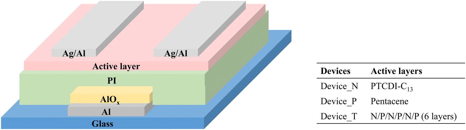 | ||
| Fig. 1 Schematic of the tandem structure-based OTFTs. | ||
2.2 Characterization
Electrical characteristics of the OTFTs were measured using a Keithley 4200-SCS semiconductor characterization system within a nitrogen-filled glove box. The photoresponse of the OTFTs was measured using blue (450 nm, 13.4 mW cm−2), green (532 nm, 10 mW cm−2), and red (633 nm, 9.8 mW cm−2) light sources. Absorbance spectra were recorded using a Hitachi U-3010S spectrometer, with wavelengths set at 405 nm for photoluminescence (PL) and time-resolved photoluminescence (TRPL) spectra. The surface potential of the thin film was measured using scanning Kelvin probe microscopy (SKPM, Park XE-100) with an atomic force microscope. X-ray diffraction (XRD) analysis was performed using a Cuka1+2 of λ = 1.54184 Å (Bruker D8 Discover), operated under standard conditions to determine the crystalline structure of the samples. The absorption spectra were recorded using a UV-visible absorption spectrometer (GBC Cintra 202, resolution < 0.9 nm) to investigate the optical properties of the materials within the wavelength range of 350–800 nm.3. Results and discussion
Here, the molecular stacking of the tandem structure film grown on the PI film was confirmed via UV-visible light absorption, as depicted in Fig. 2a. The absorption spectrum band of the PTCDI-C13 film falls within the green to blue range, while the absorption spectrum of pentacene is distributed in the red band. When PTCDI-C13 and pentacene films are stacked on top of each other to form a tandem structure, the absorption spectra of the two materials overlap, resulting in a broader absorption range. This overlapping effect enhances the overall light absorption capacity of the tandem structure, which is beneficial for photosensor applications. However, the absorption wavelength of the tandem structure at 573.3 nm exhibits a slight red shift of approximately 2 nm compared to that of the pristine PTCDI-C13 film at 571.6 nm. This shift is attributed to the tandem structure, which is composed of stacked p-type and n-type semiconductors, with the PTCDI-C13 film being initially deposited. The absorption spectrum of the tandem structure is influenced by the combined effects of the absorption peak of the pentacene film at 586.13 nm and the intrinsic absorption characteristics of PTCDI-C13, leading to the observed red shift.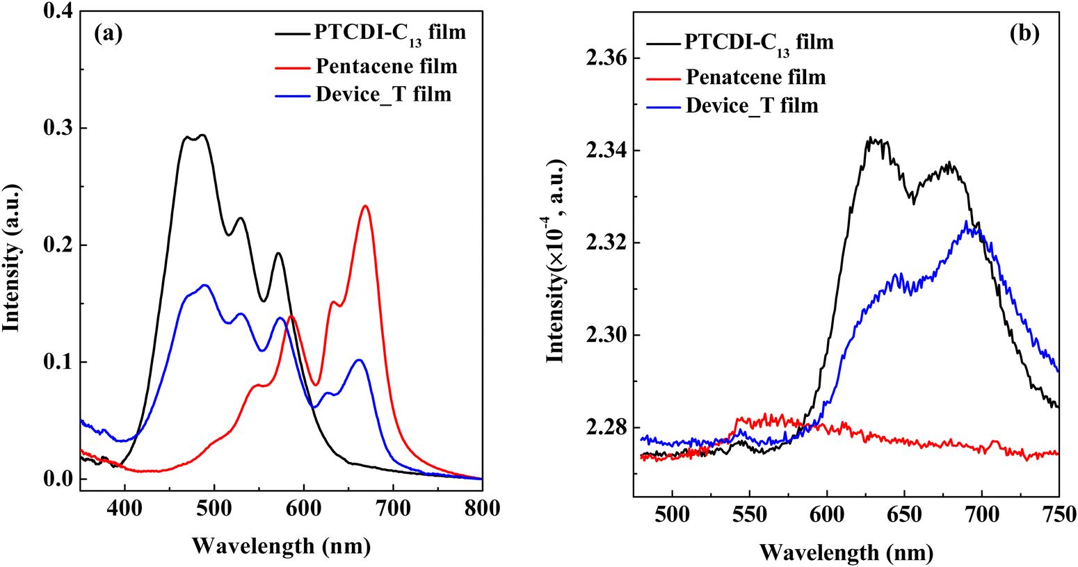 | ||
| Fig. 2 (a) Absorption spectra and (b) PL spectra of the native pentacene film, native PTCDI-C13 film, and the film with the tandem structure (Device_T). | ||
This study provides a deeper exploration of the PL behavior of organic semiconductor materials at heterojunction interfaces. A prominent peak at around 700 nm is observed in the PTCDI-C13 film, indicating its photoluminescence characteristics. As shown in Fig. 2b, the PTCDI-C13 film exhibits prominent peaks at 632 nm and 679 nm, attributed to the radiative recombination of singlet-state carriers transitioning from the conduction band to the valence band. Among these, the higher intensity at 632 nm indicates a lower exciton binding energy, facilitating exciton dissociation into free electrons and holes. Conversely, the lower intensity at 679 nm suggests a higher exciton binding energy, reducing the likelihood of exciton dissociation. In contrast, pentacene demonstrates weak emission capability due to its excitation wavelength falling outside its absorption range, resulting in negligible fluorescence signals in the PL spectrum. When the PTCDI-C13 film is combined with the pentacene film to form the tandem structure of Device_T, the electric field at the p–n heterojunction further enhances electron–hole separation, promoting exciton dissociation into free carriers. Additionally, the PL spectrum of the tandem structure exhibits a reversal in the relative intensities of the peaks at 632 nm and 679 nm compared to that of the standalone PTCDI-C13 film, further validating the modulation of PL properties at the heterojunction interface.
In the tandem structure of Device_T, even with six-layer stacking, the PL spectrum remains predominantly dominated by the emission band of PTCDI-C13, while the contribution of pentacene appears relatively weak. This phenomenon could be attributed to the enhanced electronic coupling between PTCDI-C13 and pentacene, facilitating the photoluminescence process of PTCDI-C13 molecules while suppressing the contribution of pentacene. It is noteworthy that a significant red shift is observed in the emission peak of PTCDI-C13 in the tandem structure of PTCDI-C13 and pentacene, indicating the influence of stress on the lattice of PTCDI-C13 molecules during the stacking process. This results in changes in the band structure and adjustment of the carrier formation process, leading to the observed red shift phenomenon in the photoluminescence spectrum.
In this study, we investigated the electrical characteristics of OTFTs by subjecting tandem semiconductor channels to red, green, and blue light, as illustrated in Fig. 3. Initially, when a positive bias voltage is applied to the gate and drain electrodes of Device_N, where PTCDI-C13 acts as an n-type organic semiconductor, electrons accumulate at the interface between the semiconductor and insulating layers, forming a conductive channel and generating the drain current (IDS). According to the UV-vis absorption spectrum shown in Fig. 2, PTCDI-C13 primarily absorbs light in the 495–570 nm (green) and 450–495 nm (blue) ranges but shows almost no absorption in the 630–700 nm (red) range. As a result, when Device_N is illuminated with 633 nm red light, which falls outside PTCDI-C13's primary absorption range, it fails to generate significant additional electron–hole pairs, leading to negligible changes in IDS compared to the non-illuminated device (Fig. 3a).
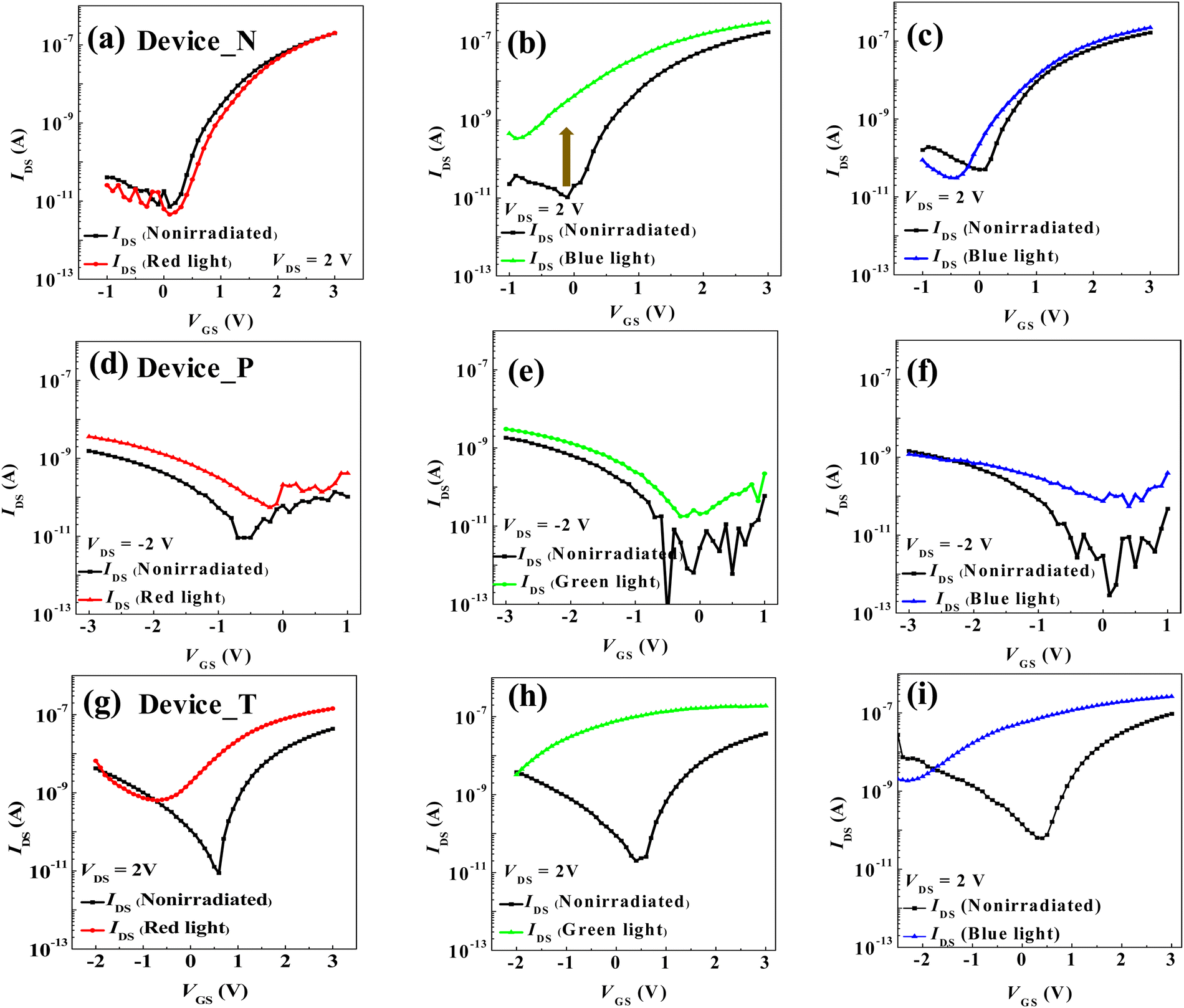 | ||
| Fig. 3 Transfer curves of Device_N (upper panel), Device_P (middle panel), and Device_T (lower panel) under illumination with red light ((a), (d) and (g)), green light ((b), (e) and (h)), and blue light ((c), (f) and (i)). | ||
In contrast, when Device_N is illuminated by 532 nm green light or 450 nm blue light, the photon energies fall within PTCDI-C13's absorption band, allowing it to generate additional electron–hole pairs. PTCDI-C13 exhibits stronger absorption of green light, resulting in a more substantial increase in the IDS under green light illumination (Fig. 3b). While blue light is also absorbed and generates carriers, it is not the optimal absorption wavelength for PTCDI-C13, leading to a smaller increase in the IDS compared to green light (Fig. 3c). This behavior is attributed to the additional free carriers generated by light absorption, which increase the total carrier concentration in the device, thus boosting the current density and causing a negative shift in the threshold voltage (Vth). However, due to the weak absorption of red light by PTCDI-C13, illumination at 633 nm does not generate significant additional carriers, resulting in minimal changes in IDS.
Fig. 3d to f reveal that the non-illuminated Device_P exhibits a saturated IDS of only 10−9 A, significantly lower than that of Device_N, indicating poorer electrical performance. X-ray diffraction (XRD) analysis (Fig. S2 and Table S1, ESI†) shows that the pentacene film has the weakest (00l) crystalline diffraction peaks, indicating poor crystallinity and molecular orientation, which leads to inferior electrical properties compared to PTCDI-C13. Under red light illumination, the IDS increases compared to the non-illuminated device, accompanied by a positive shift in the Vth (Fig. 3d). The UV-Vis absorption spectrum shows that pentacene absorbs red light effectively, generating a significant number of electron–hole pairs, which increases the carrier concentration and enhances the source–drain current. Blue light illumination, however, produces almost no increase in the IDS due to pentacene's negligible absorption in the blue range. Under green light illumination, there is a slight increase in the IDS, as pentacene absorbs weakly in this range.
For the thin-film transistor with Device_T, ambipolar characteristics are observed in its transfer curve under non-illuminated conditions, attributed to the combination of n-type and p-type semiconductors (Fig. 3g to i). Initially, when a voltage of VDS = 2 V is applied and the gate bias is swept from −2 V to 3 V, holes accumulate in the channel under a negative gate bias. As the gate bias becomes more positive, electrons accumulate, leading to hole–electron recombination and a decrease in the IDS. Eventually, electron domination in the channel occurs at a sufficiently positive gate bias, generating current.
Under red light illumination with a negative gate bias, the drain current in Device_T increases by an order of magnitude in the saturation region, and the Vth shifts negatively (Fig. 3g). Fig. 3h and i show that before illumination, the gate can still control the switching of Device_T. However, after illumination with green or blue light, the device approaches a “normally on” state, making it difficult to distinguish between the off-current and drain current, rendering the threshold voltage determination impractical. The drain current increases by approximately 102 under blue light illumination, and between 101 and 102 under green light. This discrepancy is attributed to the n-type and p-type semiconductor stacking in Device_T, forming a p–n heterojunction. Upon illumination, a large number of excitons are generated, leading to significant electron–hole pair separation at the p–n junction, causing the device to lose its gate switching capability. The XRD results indicate that the (001) peak intensity of PTCDI-C13 in Device_T is significantly higher than that of pentacene, implying superior electron transport capabilities for PTCDI-C13. This may result from PTCDI-C13 compressing the pentacene layer during stacking, leading to grain deformation and a reduction in pentacene's crystalline quality and electrical properties. The performance of various OTETs under different semiconducting materials and light irradiance is summarized in Table S2 (ESI†).
Our results demonstrate significant enhancements in the electrical performance of the light-sensing devices under illumination. To evaluate device efficiency, we calculated photosensitivity (P) and photoresponsivity (R) using eqn (1) and (2):
 | (1) |
 | (2) |
As shown in Fig. 4, when Device_N is illuminated with green light, the maximum values of P and R are approximately 301.2 and 0.12 mA W−1, respectively (summarized in Table 1). In contrast, Device_P exhibits poorer performance, with P and R values of 17.03 and 0.01 mA W−1 under red light illumination. Due to the superior light absorption and carrier mobility of PTCDI-C13, Device_N performs better under green light. Conversely, pentacene, which absorbs red light more efficiently, exhibits better performance under red light.
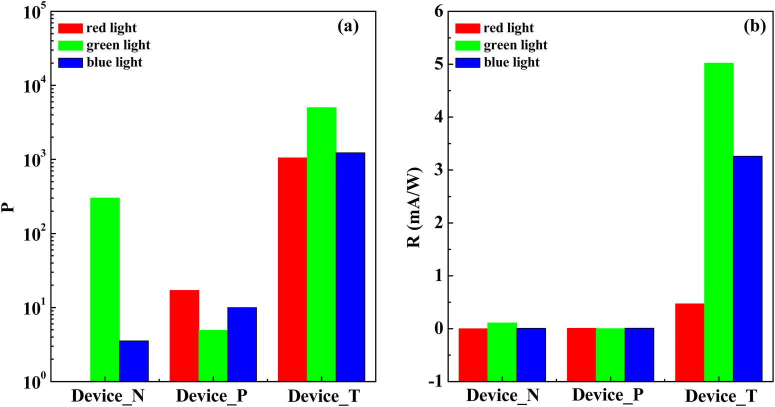 | ||
| Fig. 4 (a) Photosensitivity and (b) photoresponse performances of different photosensors. | ||
| Device_N | Device_P | Device_T | ||||
|---|---|---|---|---|---|---|
| P | R (mA W−1) | P | R (mA W−1) | P | R (mA W−1) | |
| Red light | −0.58 | <0.01 | 17.03 | 0.01 | 1051.67 | 0.47 |
| Green light | 301.22 | 0.12 | 4.93 | <0.01 | 5007.70 | 8.36 |
| Blue light | 3.56 | <0.01 | 10.00 | 0.01 | 1228.41 | 3.81 |
Device_T, with its tandem structure, shows significantly enhanced P and R values of 5007.7 and 8.36 mA W−1, respectively, under green light illumination. While red light results in slightly lower absorption performance, Device_T's photosensitivity remains comparable to that under green and blue light illumination, indicating its suitability as a full visible-spectrum light sensor. Unlike Device_N and Device_P, which are typical OTFT-based photosensors dominated by the field-effect current in the saturation region, Device_T exhibits a photovoltaic effect in the same region due to its tandem structure, enhancing stability for light-sensing applications.
Our research demonstrates that tandem semiconductor structures can significantly enhance photosensor performance. This architecture not only enables full visible-spectrum absorption but also holds potential for advancing optoelectronic devices. Future studies will explore diverse semiconductor combinations to further enhance the performance and application potential of these devices. According to a review of the literature,34–38 our device demonstrates performance in terms of operating voltage, photosensitivity, and photoresponsivity that is comparable to other studies. Notably, by employing a six-layer stack in our tandem structure, the photosensitivity significantly increased, reaching values above 5 × 10³. This high photosensitivity indicates that our structural design offers advantages in enhancing light absorption and exciton separation efficiency, which in turn improves the device's photoresponsivity performance and highlights its substantial application potential. For a comparison of our phototransistor with tandem active layers to other reports, the P and R values of various systems/materials are summarized in Table S3 (ESI†), along with the corresponding references.
TRPL analysis was performed on two OTFTs with different structures, and some interesting findings were obtained. As shown in Fig. 5, the photoluminescence decay dynamics of Device_N and Device_T exhibit significant differences. Device_N demonstrates a relatively fast decay rate, which aligns with the inherent photophysical characteristics of PTCDI-C13. In contrast, Device_T shows a noticeably slower decay curve, indicating the possibility of complex energy transfer processes occurring within its multilayer structure. Interestingly, while PTCDI-C13 generates measurable photoluminescence, pentacene fails to show detectable TRPL signals under standard measurement conditions. This phenomenon is consistent with the PL spectral results in Fig. 2. In Device_T, we observed a significant extension of the photoluminescence lifetime, which may arise from the formation of interface states between PTCDI-C13 and the pentacene layer. These interface states likely facilitate charge separation and suppress radiative recombination, leading to prolonged emission times. Although the pentacene layer does not directly contribute to the PL signal, it plays a crucial role in modulating the device's electronic structure. Furthermore, the stepped energy level structure created by the alternating stacking of PTCDI-C13 and pentacene layers may induce an energy cascading transfer mechanism, further extending the overall photoluminescence lifetime. This energy transfer process might begin with the initial excitation of PTCDI-C13, followed by rapid charge or energy transfer to the pentacene layer. Although pentacene itself does not emit light, it could serve as an intermediate state, potentially transferring energy back to PTCDI-C13 or the interface states on a longer time scale. The lifetimes for both Device_N and Device_T have been extracted from the TRPL data, as shown in Table 2. These values highlight differences in the decay behavior between the two devices, providing insights into the recombination processes at play. The shorter lifetime (τ1) of Device_T is longer than that of Device_N, indicating a higher exciton dissociation efficiency for Device_T compared to Device_N. However, the longer lifetime (τ2) of Device_T is shorter than that of Device_N, suggesting that the carrier transport length in Device_T is reduced due to its tandem structure.
 | ||
| Fig. 5 TRPL spectra of different semiconductor devices. | ||
| Semiconductor | τ 1 (ns) | τ 2 (ns) |
|---|---|---|
| Device_N | 0.45 | 3.14 |
| Device_T | 0.59 | 2.89 |
These findings highlight the substantial potential of multilayer organic semiconductor structures in tuning the optoelectronic properties of OTFTs. The enhanced charge separation and extended excited-state lifetime observed in Device_T can improve charge generation and transport, thereby potentially increasing device performance, which is also consistent with the results in Fig. 3. Importantly, the interaction between the emissive PTCDI-C13 and the non-emissive pentacene opens new avenues for designing organic optoelectronic devices with customized emission and charge transport characteristics.
SKPM enables systematic investigation of charge transfer behavior in organic semiconductor heterojunctions through precise measurements of surface potential variations, revealing the electronic properties at multiple organic semiconductor interfaces, as shown in Fig. 6a. The initial measurements focused on the electrical characteristics of the base layer. The pure PI dielectric layer exhibited a surface potential of 122 mV, with its work function approaching that of the gold–gold standard sample. This indicates that the PI layer possesses excellent electrical properties, providing a stable electronic structure foundation for the subsequent growth of organic semiconductor layers. When a 10-nm thick layer of PTCDI-C13 was grown on the PI dielectric layer, a significant increase in the surface potential was observed. This change demonstrates the formation of good interfacial contact between PTCDI-C13 and PI, contributing to reduced interface barriers and enhanced carrier transport efficiency.
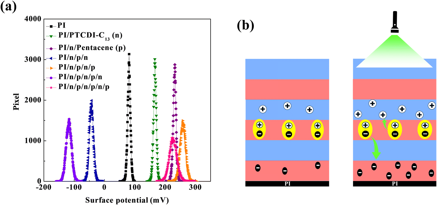 | ||
| Fig. 6 (a) SKPM images of the histogram of the LCPD values; (b) the separation of photo-induced electron–hole pairs at the p–n junction and carriers’ transport. | ||
The subsequent deposition of the pentacene layer further increased the surface potential to 231 mV, confirming that pentacene effectively grew on the PTCDI-C13 surface, consistent with our previous experimental results.39 More importantly, this stacked structure reduced the energy level difference between the highest occupied molecular orbital (HOMO) of pentacene and the lowest unoccupied molecular orbital (LUMO) of PTCDI-C13. This band alignment facilitates effective electron–hole pair separation and transport.
However, when PTCDI-C13 was further grown on the pentacene layer, the surface potential shifted negatively due to lattice mismatch effects between PTCDI-C13 and pentacene grains. This change suggests possible accumulation of additional electrons at the interface, altering the local charge distribution. This observation reveals the impact of lattice strain on charge transfer in organic semiconductor heterojunctions. In the final stage, the growth of the second pentacene layer caused surface potentials to revert to a positive value. Notably, the surface potential values remained stable from the first to the third layer of pentacene. Based on the values in Table 3, when the top layer is a pentacene film, the calculated work function closely matches the HOMO level of pentacene. In contrast, the work function of PTCDI-C13 ranges between 4.9 and 5.2 eV. Therefore, as the film stack reaches the fifth layer (i.e., a PI/n/p/n/p/n structure), the band bending in the pentacene layer accumulates additional electrons, thereby altering the local charge distribution. This phenomenon indicates that despite spatial growth constraints, the HOMO level of the p-type material (pentacene) maintained a stable position relative to the LUMO level of the n-type material (PTCDI-C13), facilitating directional electron transfer from the n-type to the p-type material. Therefore, we can confirm that when Device_T is illuminated with green light, a large number of excitons are generated, effectively leading to significant electron–hole pair separation at the p–n junction, resulting in an increase in the photocurrent, as shown in Fig. 6b.
| Tandem layers | Surface potential (mV) | Work function (eV) |
|---|---|---|
| PI | 122 | 4.978 |
| PI/PTCDI-C13 (n) | 166 | 4.934 |
| PI/n/pentacene (p) | 231 | 4.869 |
| PI/n/p/n | −4.3 | 5.143 |
| PI/n/p/n/p | 259 | 4.841 |
| PI/n/p/n/p/n | −118 | 5.218 |
| PI/n/p/n/p/n/p | 227 | 4.873 |
4. Conclusions
Our research reveals that employing stacked structures of organic semiconductors can significantly improve the optoelectronic response and broadband light absorption capabilities of optoelectronic devices. By carefully designing p–n heterojunctions, we can achieve efficient exciton dissociation and transport, dramatically enhancing the device's photoconversion efficiency. The fabricated heterojunction OTFTs exhibit outstanding optoelectronic responses across the visible spectrum, with the maximum photosensitivity and photoresponsivity reaching as high as 5007.7 and 8.36 mA W−1, respectively, far surpassing those of conventional single-layer active devices. Notably, the synergistic interactions between different semiconductor layers in the stacked OTFTs give rise to emergent optoelectronic behaviors. Through time-resolved spectroscopic studies, we have unveiled the exciton decay dynamics within these segmented conjugated polymer heterojunctions. The fast and slow decay components correspond to interfacial exciton transfer and effective geminate exciton capture processes, respectively. Rapid exciton dissociation and delivery can suppress triplet exciton formation and non-radiative quenching, thereby optimizing the device's photoconversion efficiency. This research not only expands our understanding of organic optoelectronic conversion mechanisms but also provides new strategies for designing high-performance, broadband optoelectronic devices. By judiciously selecting material combinations and optimizing the stacked architecture, we can achieve further enhancements in light absorption and exciton dissociation efficiencies, leading to improved photoconversion performance. This advancement will drive the development of organic optoelectronic conversion technologies in applications such as flexible photodetection and artificial retinal implants. Our work paves a promising path and offers new insights into the development of high efficiency photoconversion devices.Author contributions
Wei-Yang Chou: conceptualization, methodology, project administration, and writing review & editing; Po-Hsiang Fang: data curation, formal analysis, and writing original draft; Zhao-Lun Kuo and Yu-Tong Wu: investigation and validation; Horng-Long Cheng: formal analysis.Data availability
Data will be made available on request.Conflicts of interest
The authors declare that they have no known competing financial interests or personal relationships that could have appeared to influence the work reported in this paper.Acknowledgements
The authors acknowledge the financial support from the National Science and Technology Council of Taiwan (NSTC113-2221-E-006 -109 and 113-2112-M-006 -023) and the use of XRD005100 of NSTC 113-2740-M-006-002 belonging to the Core Facility Center of National Cheng Kung University.Notes and references
- W. Tang, Y. K. Huang, L. Han, R. L. Liu, Y. Z. Su, X. J. Guo and F. Yan, J. Mater. Chem. C, 2019, 7, 790–808 RSC.
- M. Mamada, H. Shima, Y. Yoneda, T. Shimano, N. Yamada, K. Kakita, T. Machida, Y. Tanaka, S. Aotsuka, D. Kumaki and S. Tokito, Chem. Mater., 2015, 27, 141–147 CrossRef CAS.
- H. J. Jeong, S. H. Baek, S. G. Han, H. Y. Jang, S. H. Kim and H. S. Lee, Adv. Funct. Mater., 2018, 28, 1704433 CrossRef.
- Z. Y. Zhao, K. Liu, Y. W. Liu, Y. L. Guo and Y. Q. Liu, Natl. Sci. Rev., 2022, 9, nwac090 CrossRef CAS PubMed.
- G. S. Ryu, J. S. Kim, S. H. Jeong and C. K. Song, Org. Electron., 2023, 14, 1218–1224 CrossRef.
- C. Y. Ke, M. N. Chen, Y. C. Chiu and G. S. Liou, Adv. Electron. Mater., 2021, 7, 2001076 CrossRef CAS.
- Z. S. Qin, T. Y. Wang, H. K. Gao, Y. Li, H. L. Dong and W. P. Hu, Adv. Mater., 2023, 35, 2301955 CrossRef CAS.
- D. H. Lee, H. S. Cho, D. Han, R. Chand, T. J. Yoon and Y. S. Kim, J. Mater. Chem. B, 2017, 5, 3580–3585 RSC.
- K. Asano, Y. Sasaki, Q. Zhou, R. Mitobe, W. Tang, X. J. Lyu, M. Kamiko, H. Tanaka, A. Yamagami, K. Hagiya and T. Minami, J. Mater. Chem. C, 2021, 9, 11690–11697 RSC.
- Y. V. D. Burgt, A. Melianas, S. T. Keene, G. Malliaras and A. Salleo, Nat. Electron., 2018, 1, 386–397 CrossRef.
- J. L. Shi, J. S. Jie, W. Deng, G. Luo, X. C. Fang, Y. L. Xiao, Y. J. Zhang, X. J. Zhang and X. H. Zhang, Adv. Mater., 2022, 34, 2200380 CrossRef CAS PubMed.
- E. Bystrenova, M. Jelitai, I. Tonazzini, A. N. Lazar, M. Huth, P. Stoliar, C. Dionigi, M. G. Cacace, B. Nickel, E. Madarasz and F. Biscarini, Adv. Funct. Mater., 2008, 18, 1751–1756 CrossRef CAS.
- K. J. Baeg, M. Binda, D. Natali, M. Caironi and Y. Y. Noh, Adv. Mater., 2013, 25, 4267–4295 CrossRef CAS PubMed.
- G. Y. Wei, Z. Lu, Y. C. Cai and C. H. Sui, Mater. Lett., 2017, 201, 137–139 CrossRef CAS.
- C. Xie, P. You, Z. Liu, L. Li and F. Yan, Light: Sci. Appl., 2017, 6, e17023 CrossRef PubMed.
- Z. Kişnişci, Ö. F. Yüksel and M. Kuş, Synth. Met., 2014, 194, 193–197 CrossRef.
- M. R. F. Silva, M. F. R. P. Alves, J. P. G. Q. Cunha, J. L. Costa, C. A. Silva, M. H. V. Fernandes, P. M. Vilarinho and P. Ferreira, Mater. Today Phys., 2023, 35, 101131 CrossRef CAS.
- J. M. Szarko, B. S. Rolczynski, S. J. Lou, T. Xu, J. Strzalka, T. J. Marks, L. P. Yu and L. X. Chen, Adv. Funct. Mater., 2014, 24, 10–26 CAS.
- C. F. Lin, M. Zhang, S. W. Liu, T. L. Chiu and J. H. Lee, Int. J. Mol. Sci., 2011, 12, 476–505 CrossRef CAS PubMed.
- J. M. Su, Y. Z. Li, Y. H. Chang, M. Z. Li, W. Z. Qiu, S. W. Liu and K. T. Wong, Mater. Today Energy, 2021, 20, 100633 CrossRef CAS.
- S. J. Sung, J. H. Kim, S. H. Gihm, J. Park, Y. S. Cho, S. J. Yang and C. R. Park, ACS Appl. Energy Mater., 2019, 2, 8826–8835 CrossRef CAS.
- C. M. Zhong, H. S. Choi, J. Y. Kim, H. Y. Woo, T. L. Nguyen, F. Huang, Y. Cao and A. J. Heeger, Adv. Mater., 2015, 27, 2036–2041 CrossRef CAS.
- S. Athanasopoulos, S. Tscheuschner, H. Bässler and A. Köhler, J. Phys. Chem. Lett., 2017, 8, 2093–2098 CrossRef CAS PubMed.
- D. B. Yang, Y. Jiao, L. Yang, Y. Chen, S. Mizoi, Y. Huang, X. M. Pu, Z. Lu, H. Sasabe and J. J. Kido, J. Mater. Chem. A, 2015, 3, 17704–17712 RSC.
- P. Amsalem, J. Niederhausen, A. Wilke, G. Heimel, R. Schlesinger, S. Winkler, A. Vollmer, J. P. Rabe and N. Koch, Phys. Rev. B: Condens. Matter Mater. Phys., 2013, 87, 035440 CrossRef.
- L. Packman, N. Mallo, A. Raynor, M. Gao, M. Babazadeh, H. Jin, D. M. Huang, P. L. Burn, I. R. Gentle and P. E. Shaw, Phys. Chem. Chem. Phys., 2023, 25, 23867–23878 RSC.
- W. L. Su, G. L. Ran, Y. Zhang, Y. H. Liu, H. Lu, Z. S. Bo and W. K. Zhang, J. Phys. Chem. C, 2023, 127, 8119–8125 CrossRef CAS.
- D. Ji, J. Y. Go, S. Jeon, Y. J. Kim, J. W. Min, K. W. Cho, B. Lim and Y. Y. Noh, Dyes Pigm., 2023, 210, 111040 CrossRef CAS.
- H. Imahori, Bull. Chem. Soc. Jpn., 2023, 96, 339–352 CrossRef CAS.
- S. S. Gao, S. Q. Wang, J. Y. Wu and Z. H. Lin, J. Mater. Chem. C, 2023, 11, 16890–16911 RSC.
- A. Dolan, X. Pan, M. J. Griffith, A. Sharma, J. M. de la Perrelle, D. Baran, G. F. Metha, D. M. Huang, T. W. Kee and M. R. Andersson, Adv. Mater., 2024, 36, 2309672 CrossRef CAS PubMed.
- P. Cusumano, C. Arnone, M. A. Giambra and A. Parisi, Electronics, 2020, 9, 70 CrossRef CAS.
- T. Nakamura, Y. Ishikura, N. Arakawa, M. Hori, M. Satou, M. Endo, H. Masui, S. Fuse, T. Takahashi, Y. Murata, R. Murdey and A. Wakamiya, RSC Adv., 2019, 9, 7107–7114 RSC.
- C. Tozlua, M. Kus, M. Cand and M. Ersöz, Thin Solid Films, 2014, 569, 22–27 CrossRef.
- D. E. Lee, J. H. Oh and E. K. Lee, ACS Appl. Mater. Interfaces, 2024, 16, 51221–51228 CrossRef CAS.
- Z. Jagoo, Z. A. Lamport, O. D. Jurchescu and L. E. McNeil, ACS Appl. Electron. Mater., 2022, 4, 5799–5808 CrossRef CAS.
- D. Bharti, V. Raghuwanshi, I. Varun, A. K. Mahato and S. P. Tiwari, IEEE Sens. J., 2017, 17, 12 Search PubMed.
- H. Alzahrani, K. Sulaiman, A. Y. Mahmoud and R. R. Bahabry, Synth. Met., 2021, 278, 116830 CrossRef CAS.
- W. Y. Chou, S. K. Peng, F. C. Wu, H. S. Sheu, Y. F. Wang, P. K. Huang and H. L. Cheng, J. Mater. Chem. C, 2020, 8, 7501–7508 RSC.
Footnote |
| † Electronic supplementary information (ESI) available. See DOI: https://doi.org/10.1039/d4tc04467c |
| This journal is © The Royal Society of Chemistry 2025 |