
 Open Access Article
 This Open Access Article is licensed under a Creative Commons Attribution-Non Commercial 3.0 Unported Licence
High performance BaTiO3–SrTiO3 ceramics with refined microstructure obtained by current-controlled reactive flash sintering of mixed powders†
Samuel
López-Blanco
 *a,
Xavier
Vendrell
b,
Nerea
Morante
b and
José E.
García
*a
*a,
Xavier
Vendrell
b,
Nerea
Morante
b and
José E.
García
*a
aDepartment of Physics, Universitat Politècnica de Catalunya, 08034 Barcelona, Spain. E-mail: jose.eduardo.garcia@upc.edu; samuel.lopez.blanco@upc.edu
bDepartment of Inorganic and Organic Chemistry, Universitat de Barcelona, 08028 Barcelona, Spain
First published on 27th December 2024
Abstract
Barium strontium titanate is a well-known perovskite-structured ferroelectric system that has recently gained attention for its energy storage capabilities. Here, fine-grained BaTiO3–SrTiO3 ceramics are obtained by reactive flash sintering of mixed BaTiO3 and SrTiO3 powders, a one-step sintering process that significantly reduces the energy consumption involved. The current control mode is employed here to manage the reactive flash sintering event for a striking refinement of the microstructure. The effect of microstructure on the dielectric, ferroelectric, and energy storage properties of flash-sintered ceramics is discussed through the analysis of impedance spectroscopy data. The quality and electrical homogeneity of the obtained materials are shown to be key factors in optimizing the energy storage properties of dielectric materials. This work highlights the potential of current-controlled flash sintering as a powerful tool for microstructural engineering in dielectric materials, offering new pathways for the development of energy-efficient energy storage systems.
1 Introduction
Barium strontium titanate (Ba1−xSrxTiO3) is a perovskite-structured ferroelectric system that is part of the widely studied A-site substituted BaTiO3 family of materials.1–3 The substitution of Ba2+ for Sr2+ efficiently shifts the phase transition of the BaTiO3 toward room temperature while the cationic disorder broadens the phase transition, thereby reducing the temperature dependence of the resulting functional properties.4,5 Consequently, Ba1−xSrxTiO3 (BST) has been taken under consideration mainly as dielectric bolometers for infrared detection, tunable capacitors for microwave devices and pyroelectric imaging detectors.6–10 Recently, however, BST has gained great attention due to its potential applications in energy storage because it possesses relatively high energy storage density and efficiency, remarkable breakdown strength, and good reliability.11Theoretical and experimental studies have evidenced that the Ba/Sr ratio can greatly influence the energy storage properties of BST ceramics depending on the operating electric field.12,13 Thus, compositions with high Sr content (i.e., linear dielectrics) are desirable for high working electric fields (>300 kV cm−1), but these materials show low dielectric permittivity and are limited by the breakdown strength they can reach (typically lower than 300 kV cm−1).14 Therefore, BST compositions commonly explored for energy storage are those with x = 0.5–0.7, though the published results are diverse.15–20 Hence, not only are different results reported for the same composition, but similar energy storage properties are also achieved from compositions with different Ba/Sr ratios, which can be explained in terms of the grain size effect.
The effect of grain size on the energy storage properties of electroceramics is widely discussed in the literature.21 Grain size engineering has been proven to be an efficient strategy for simultaneously improving energy storage performance and mechanical properties in lead-free perovskite ferroelectrics.14,22 In BST, particularly, although some functional properties certainly worsen as grain size decreases,23,24 the energy storage performance has been demonstrated to enhance.19,20 It has been shown that compositions with different Sr content experience an enhancement in their energy storage properties through proper microstructure control, primarily related to an improvement in electrical breakdown strength. In general terms, smaller grains down to the submicron scale yield higher energy storage performance.
Dense, fine-grained BST ceramics has been generally obtained by spark plasma sintering,19,20,23,25 a well-known technique that require a rather complex and expensive equipment. Recently, however, Ba0.6Sr0.4TiO3 was successfully flash-sintered from powders prepared via the conventional solid-state reaction method using BaCO3, SrCO3, and TiO2, resulting in a fine-grained microstructure that enhances its properties as a tunable dielectric ceramic.26 In this work, we use current-controlled reactive flash sintering of mixed BaTiO3 and SrTiO3 powders to obtain highly dense BST ceramics with a refined microstructure, aimed at improving energy storage performance. Flash sintering is a novel, low-energy consumption, and significantly cheap field-assisted sintering route that is attracting growing interest because dense ceramics can be obtained in few minutes and at relatively low temperatures.27,28 A considered suboptimal composition, namely Ba0.6Sr0.4TiO3, is taken here as a reference to demonstrate that microstructure control is the definitive key factor for improving the energy storage capabilities of ferroelectric ceramic systems.
2 Experimental
2.1 Sintering experiments
Reactive flash sintered samples are obtained by performing flash sintering experiments using commercially available BaTiO3 and SrTiO3 powders as precursors. Barium titanate (Sigma Aldrich, ≥99.5%, Ref. 338842-100G) and strontium titanate (Sigma Aldrich, ≥99%, Ref. 396141-100G), both with particle size of <2 μm, were used in a molar ratio of 60![[thin space (1/6-em)]](https://www.rsc.org/images/entities/char_2009.gif) :40 to produce the Ba0.6Sr0.4TiO3 composition. Green samples (GS) are formed by uniaxial pressing the powder into a dog bone shape using a load of 270 MPa (Fig. S1a, ESI†). To perform the sintering experiments, GS is hanged in the centre of the furnace using two platinum wires attached to its handles following a typical flash sintering setup (Fig. S1b, ESI†). A programable DC power supply (Ametek XG 600-2.6) is controlled employing a homemade software, changing its operation mode automatically upon reaching the previously set current limit. In order to ensure electrical contact between the sample and the platinum wire electrodes, platinum paint is used (SPI supplies, 04990-AB) mixed with platinum paint thinner (SPI supplies, 04989-AB). The use of an adequate paint geometry allows to obtain a uniform electric current flow across the sample by mimicking a plane parallel capacitor (Fig. S1a, ESI†). Luminescence and shrinkage of the samples are recorded with a CCD camera.
:40 to produce the Ba0.6Sr0.4TiO3 composition. Green samples (GS) are formed by uniaxial pressing the powder into a dog bone shape using a load of 270 MPa (Fig. S1a, ESI†). To perform the sintering experiments, GS is hanged in the centre of the furnace using two platinum wires attached to its handles following a typical flash sintering setup (Fig. S1b, ESI†). A programable DC power supply (Ametek XG 600-2.6) is controlled employing a homemade software, changing its operation mode automatically upon reaching the previously set current limit. In order to ensure electrical contact between the sample and the platinum wire electrodes, platinum paint is used (SPI supplies, 04990-AB) mixed with platinum paint thinner (SPI supplies, 04989-AB). The use of an adequate paint geometry allows to obtain a uniform electric current flow across the sample by mimicking a plane parallel capacitor (Fig. S1a, ESI†). Luminescence and shrinkage of the samples are recorded with a CCD camera.
Conventional reactive flash sintering (RFS) and current-controlled reactive flash sintering (CRFS) experiments (Fig. S2, ESI†) are carried out to study the influence of the electric parameters over the resulting samples’ density and microstructure. For the case of RFS experiments, the furnace is heated from room temperature at a rate of 10 °C min−1 while the sample helds under a constant electric field. When the flash event takes place (i.e., the current runaway) the power source changes to constant current mode and the sample is left to dwell for a set time. Finally, the furnace is shut down and the sample cools down naturally. For the case of CRFS experiments, the furnace is heated once again using a rate of 10 °C min−1 from room temperature up until a preset temperature, which depends on the specific experiment, but no electric field is preset. The samples are then held exclusively in current control mode until reaching the maximum preset current, when they are then left to dwell for a set time. After finishing the experiment, the furnace is shut down and the samples are left to cool down naturally.
2.2 Microstructure and functional characterization
In order to ensure reproducibility and minimize inhomogeneities, the sintered specimens are cut far from the vicinity of the electrical contacts in rectangular cuboid shape (10 mm × 3 mm × 1 mm). Density is measured via Archimedes method. Field-emission scanning electron microscope measurements (FESEM JEOL-7100) are performed in polished and thermally etched samples. X-ray diffraction patterns of dense samples were obtained from a PANalytical X’Pert PRO MPD diffractometer with CuKα radiation. The electrical characterization of the specimens is done after the application of electrical contacts via gold sputtering. Permittivity values of unpoled samples are measured using an LCR meter (Agilent E4980A) from approximately 400 K to 20 K using frequencies that range from 100 Hz up to 1 MHz. Electric field-induced polarization (P−E) hysteresis loops are obtained using a typical Sawyer–Tower setup by applying a triangular electric field of up to 5 kV mm−1 at a frequency of 1 Hz at room temperature. Impedance spectroscopy experiments are conducted with a frequency response analyser (AMETEK solartron analytical). Impedance measurements are taken across a frequency range from 100 mHz to 1 MHz at various temperatures. The samples are heated in a furnace from room temperature with a ramp rate of 5 °C min−1 until the target temperature is reached. At this point, the sample is allowed to stabilize thermally for 10 min.3 Results and discussion
3.1 Reactive flash sintering
A comprehensive study about the influence of the flash sintering parameters over the densification and microstructure of BaTiO3 (BTO) has been recently published,29 which has served as the basis for the RFS experiments of BaTiO3 and SrTiO3 mixed powders. A set of electrical conditions were employed in order to attempt high densification of the resulting Ba0.6Sr0.4TiO3 composition. Results are recorded in Fig. S3 (ESI†), showing that low electric fields and moderate electric current densities (15–30 mA mm−2) yield better results. Although RFS experiments were not successful in achieving highly dense specimens, best results have been considered as starting point for the CRFS experiments. The current control is an emerging parameter in flash sintering that has recently gained attention.29–33 It is known to both enhance densification and be closely related to defect formation and microstructure tailoring during flash sintering. In CRFS experiments, the furnace temperature is set constant, and therefore, the sample accommodates an appropriate electric field to maintain the desired electric current, which slowly rises. This approach avoids the sudden power spike of the flash event and minimizes temperature gradients, thereby ensuring a homogeneous sintering. Undoubtedly, these experiments require controlling a higher number of parameters such as the electric profile and current slope, which may initially seem like a hindrance. However, the CRFS technique provides a powerful set of tools that allow fine-tuning the microstructure. In fact, previous studies suggest that CRFS experiments not only finely tune functional properties and enhance densification, but also provide a new path to precisely achieve defect-engineered microstructures.29,34Fig. 1 shows the resulting density of flash-sintered Ba0.6Sr0.4TiO3 specimens for several CRFS configurations. First, the effect of the furnace temperature was evaluated by keeping a maximum current density of 15 mA mm−2 and a dwell time of 5 min. Results show that a furnace temperature of 1200 °C yields good densification, and therefore, no higher temperatures were assessed. Next, various dwell times were explored showing that 5 min seems to be an optimal time to ensure high densification. In this case, a maximum current density of 15 mA mm−2 and a furnace temperature of 1200 °C were used. Finally, a set of maximum current densities was tested since it is well-known that current density is a key parameter for fine-tuning the sample's microstructure in flash sintering.29,35,36 High densification (i.e., higher than 90%) is achieved for a current density range of 10–25 mA mm−2, with a furnace temperature of 1200 °C and a dwell time of 5 min. Poor densification is expected for lower furnace temperature and/or a different dwell time.
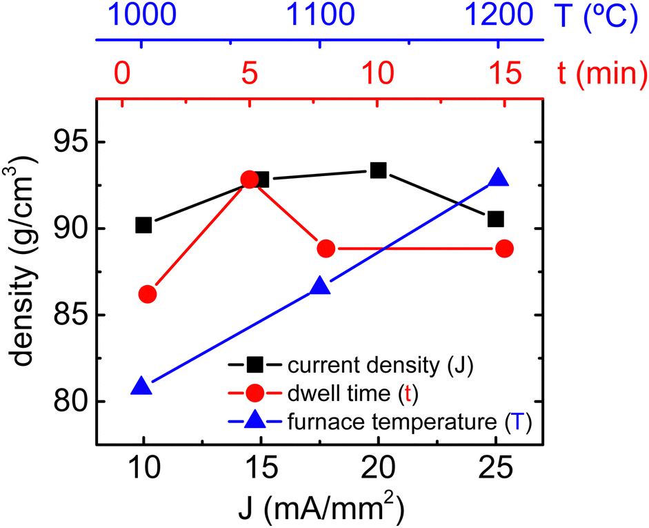 | ||
| Fig. 1 Density of CRF-sintered Ba0.6Sr0.4TiO3 samples upon different electrical condition. Different furnace temperatures were tested while keeping the current density and dwell time constant at 15 mA mm−2 and 5 min, respectively. Various dwell times were then used maintaining the furnace temperature and the current density at 1200 °C and 15 mA mm−2, respectively. Finally, several current densities were explored while keeping the furnace temperature and the dwell time at 1200 °C and 5 min, respectively, which correspond to the optimal conditions from the previous experiments. Only current densities yielding a density higher than 90% were considered. | ||
3.2 Microstructure and electrical properties
Samples exhibiting poor density (i.e., lower than 90%) are discarded for further characterizations. Therefore, Fig. 2 and 3 show dielectric and ferroelectric properties only of the high-density samples, which are labelled as CRFS/x, with x being the maximum current density at which each of them was sintered by CRFS. Real permittivity and dielectric losses versus temperature curves (Fig. 2) show slight differences between the samples. The real permittivity peak associated with the ferroelectric–paraelectric transition of Ba0.6Sr0.4TiO3 is observed at 279 K, except for the CRFS/10 sample, where it is 10 degrees lower. Other two anomalies are also observed for CRFS/15, CRFS/20, and CRFS/25 samples, which correspond to the expected tetragonal–orthorhombic and orthorhombic–rhombohedral phase transitions.4 However, these anomalies are not as evident in the CRFS/10 sample, where an apparent single peak is revealed, although dielectric losses indicate the presence of more than one phase transition. Both the broadening of the real permittivity curve and the shift of the phase transition temperature are common features of grain size effect. The noticeable differences in maximum real permittivity could be related to the samples' density (Table 1), although in the case of the CRFS/10 sample, grain size effects make this correlation more complex. No frequency dispersion in the dielectric response is observed in any of samples (Fig. S4, ESI†). Typical ferroelectric hysteresis loops are displayed in Fig. 3 for all selected CRF sintered samples, showing notable difference depending on the sintering condition. Particularly, it can be seen that the sample CRFS/15 stands out from the rest owing to its extremely slim ferroelectric response, making it ideal for energy storage purposes.11,21,37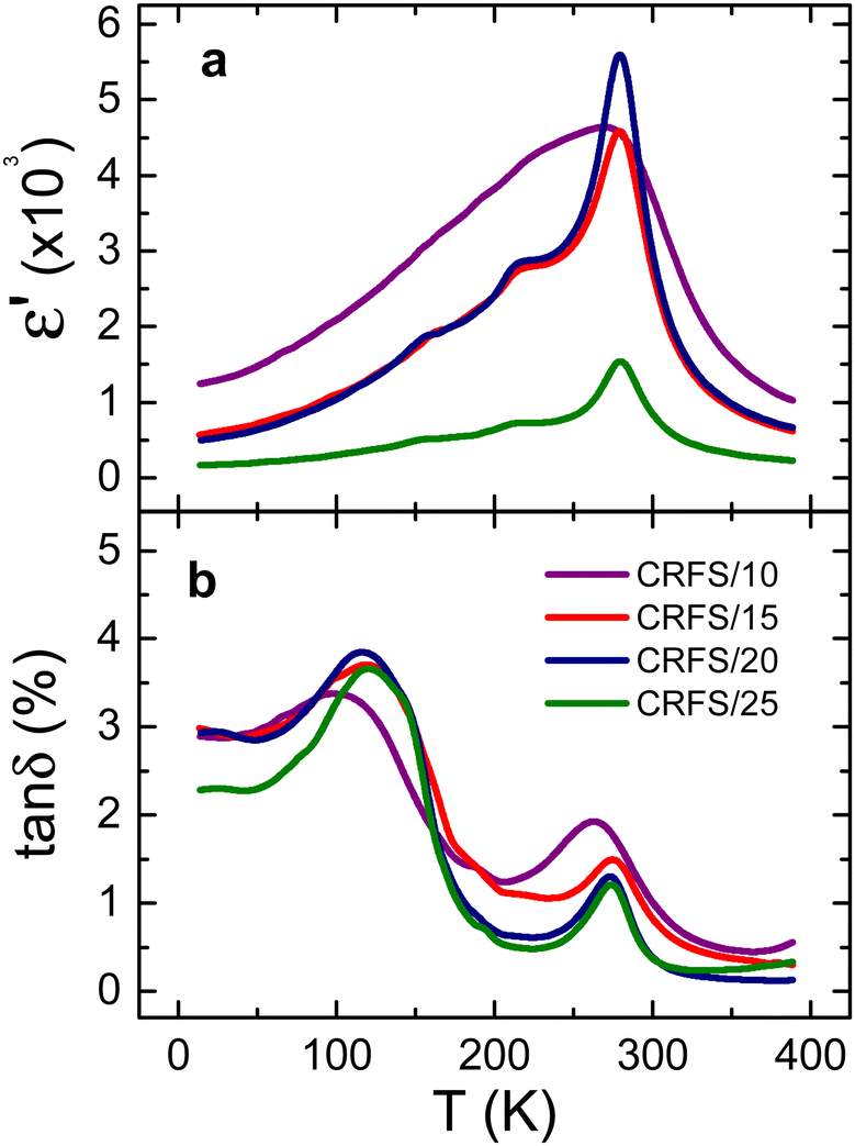 | ||
| Fig. 2 Dielectric properties of the representative CRF-sintered Ba0.6Sr0.4TiO3 samples. Temperature dependence of (a) real permittivity and (b) dielectric losses for all selected samples, at 10 kHz. Noticeable differences depending on the maximum current density employed during CRFS is shown. | ||
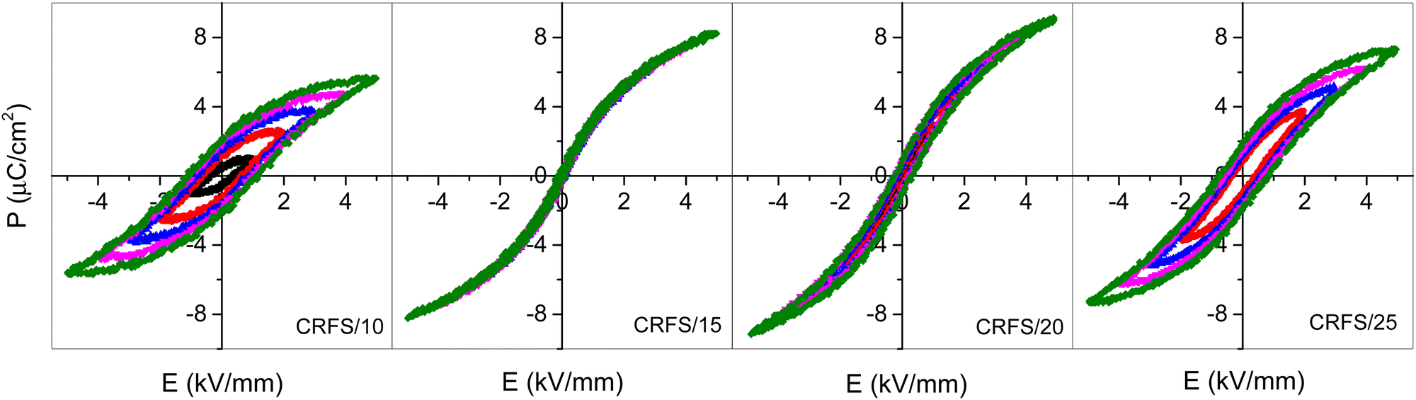 | ||
| Fig. 3 Ferroelectric properties of the representative CRF-sintered Ba0.6Sr0.4TiO3 samples. P−E hysteresis loops show appreciable differences depending on the current density, highlighting that a fully slim P−E response is evidenced when Ba0.6Sr0.4TiO3 is obtained with a particular combination of furnace temperature and electrical conditions during CFRS. | ||
δ) properties of dense flash-sintered samples. Sintering conditions (current density, J, furnace temperature, T, and dwell time, t), density, medium grain size (GS), and the temperature of the real permittivity peak (Tm) are also reported for all samples
| CRFS/10 | CRFS/15 | CRFS/20 | CRFS/25 | |
|---|---|---|---|---|
| J (mA mm−2) | 10 | 15 | 20 | 25 |
| T (°C) | 1200 | 1200 | 1200 | 1200 |
| t (min) | 5 | 5 | 5 | 5 |
| Density (%) | 90.2 | 92.8 | 93.3 | 90.5 |
| GS (μm) | 3.64 | 4.27 | 5.84 | 5.77 |
| T m (K) | 269 | 279 | 279 | 279 |
| ε′ | 3850 | 2870 | 3100 | 870 |
| Tanδ (%) |
1.04 | 1.00 | 4.57 | 5.64 |
| E C (kV mm−1) | 1.08 | 0.10 | 0.50 | 0.77 |
| P r (μC cm−2) | 1.94 | 0.30 | 1.71 | 1.94 |
| P s (μC cm−2) | 5.67 | 8.23 | 8.21 | 7.31 |
Table 1 records sintering conditions and some properties of the selected samples. It is worth noting that room temperature dielectric properties are quite different, with samples sintered at lower current densities exhibiting better properties (i.e., high dielectric constant and low losses). The highest dielectric constant value of the CRFS/10 sample seems to be related to the permittivity peak broadening. However, this sample achieves the worst maximum polarization. On the contrary, the CRFS/15 sample exhibits the highest value of maximum polarization along with an extremely low value of remnant polarization. In order to analyse the origin of this feat, a comparison of the samples’ microstructure is first conducted. Fig. 4(a–d) shows a clear dependence between the resulting microstructure and the maximum current density employed. Finer grains and lower grain size dispersion seem to be obtained with lower current densities, as shown in Fig. 4e–h. However, the apparent refined microstructure of the CRFS/10 sample does not correlate with its poor functional response. Given the high density of the samples (Table 1), the porosity observed in Fig. 4(a–d) can be attributed to the polishing process. Home-made polishing tools, consisting of high-speed rotating disks coated with diamond paste, were used for sample preparation. These harsh conditions may have dislodged small fragments from the samples prior to SEM imaging.
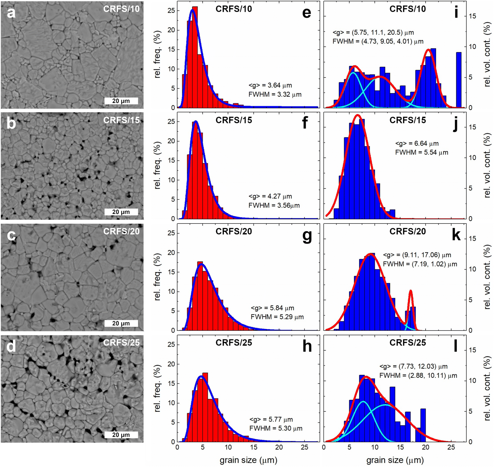 | ||
| Fig. 4 Microstructure of CRF-sintered Ba0.6Sr0.4TiO3 samples. (a–d) Micrographs of samples obtained by CRFS using different current density. (e–h) Grain size distribution for each sample. The relative frequency of occurrence of each grain size is shown. The obtained average grain size (〈g〉) and the size dispersion (FWHM) are reported in each panel, showing that both tend to increase with the current density. (i–l) Grain size volume contribution of representative CRFS specimens. The relative volume contribution of each grain is plotted, evidencing that the microstructure homogeneity heavily depends on the current density during CRFS. The obtained average grain sizes (〈g〉) and size dispersions (FWHM) are reported in each panel, showing that only the CRFS/15 sample exhibits a monomodal microstructure. | ||
Image analysis software allows the calculation of the individual area of all grains visualized in an SEM image. The grain diameters are determined by approximating each measured area to a circle. Once the diameters are calculated, individual grain volumes can be estimated by approximating each grain to a sphere. Then, the volume contribution can be obtained as the volume occupied by grains of a given size relative to the total volume of all grains. By carefully inspecting the grain size by volume contribution (Fig. 4i–l), important microstructural features emerge. It becomes evident that apparently refined microstructures are actually quite heterogeneous. For instance, the grain size by volume contribution in CRFS/10 reveals that this sample has a trimodal microstructure with similar volumetric contributions from each mode. The sample CRFS/15, however, has the most homogeneous microstructure; i.e., it appears to be the only monomodal sample. This specimen has previously shown an excellent ferroelectric response for energy storage capabilities. Therefore, it is possible to hypothesize that the extremely slim ferroelectric response of the CRFS/15 sample may be due to microstructure refinement.
Elucidating the mechanisms involved in the evolution of the microstructure requires a detailed analysis of phase formation and densification for each sample. Although this analysis is beyond the scope of this work due to its scientific and technical complexity, EDX results (Fig. S5, ESI†) allow us to hypothesize that the abnormal grain size distribution observed when the sample is flash-sintered at 10 mA mm−2 is due to the localization of flash sintering in SrTiO3-rich regions. At 15 mA mm−2, the current is sufficiently high to enable homogeneous sintering throughout the sample (but not so high as to induce abnormal grain growth), resulting in a uniform microstructure. At even higher currents, the microstructure becomes bimodal again due to the well-known abnormal grain growth that occurs during flash sintering at high currents, resulting from the localized melting of grains. XRD patterns of the representative samples (Fig. S6, ESI†) show no evidence of undesired phases, with all patterns indicating a cubic perovskite structure, as expected for a Ba0.6Sr0.4TiO3 composition at room temperature.4,26
Energy storage capabilities of the CRFS/15 sample are shown in Fig. 5. The energy storage density and efficiency were computed from the unipolar P−E loops (Fig. S7, ESI†) as is usually reported in the literature (some details about the calculation procedure are given in Fig. S8, ESI†).11,14,37 As shown, the energy that can be stored increases with the applied electric field, while at the same time, the energy storage efficiency decreases, as commonly reported for this and other systems.17,18,22 The values of the recovered energy density were computed until the energy storage efficiency dropped below 85%. The obtained values are in accordance with previous results in Ba1−xSrxTiO3 system (Fig. S9, ESI†),15–20 but with one significant difference: an optimal composition of Ba1−xSrxTiO3 for energy storage is expected for x = 0.5–0.7. Therefore, a composition a priori considered as suboptimal (x = 0.4) achieves similar energy storage properties to those expected for more optimal compositions. This fact must be related to the microstructure refinement attained by CRFS. At this juncture, an important question emerges: why does a refined, more homogeneous microstructure show better electrical properties?
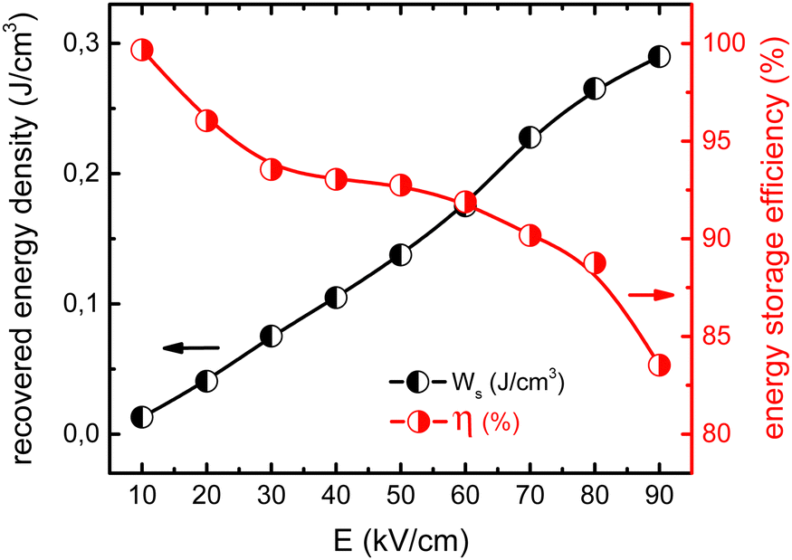 | ||
| Fig. 5 Energy storage properties of CRF-sintered Ba0.6Sr0.4TiO3 sample at a current density of 15 mA mm−2 (CRFS/15). Energy storage density and energy storage efficiency of CRFS/15 are plotted as a function of the applied electric field. While the energy storage increases, the energy efficiency decreases. | ||
The concept of electrical microstructure, understood as a measure of the quality and electrical homogeneity of materials, has been proposed as one of the key factors for optimizing energy storage properties of dielectric ceramics.21 A homogeneous distribution of local conductivity has been proved to be an important feature to enhance energy storage.38 Impedance spectroscopy is recognized as a powerful tool for evaluating the electrical microstructure, as there is a link between microstructure and the AC electrical response of electroceramics.39
In the analysis of impedance data of electroceramics, it is standard practice to present the data using impedance complex plane plots, Z′′/Z′ (Z*). A representative complex plane plot recorded at 400 °C for the CRFS/20 sample is shown in Fig. 6c. The Z* plot shows two components: one semicircle at high frequencies and another at lower frequencies. The high frequency and lower frequency semicircles could be modelled, to a first approximation, on two parallel resistor–capacitor (RC) elements in series. The associated capacitances, ∼20 pF cm−1 at high frequencies and ∼2 nF cm−1 at lower frequencies are typical of bulk and grain boundary responses, respectively.38 All samples showed similar behaviour at different temperatures (Fig. S10, ESI†).
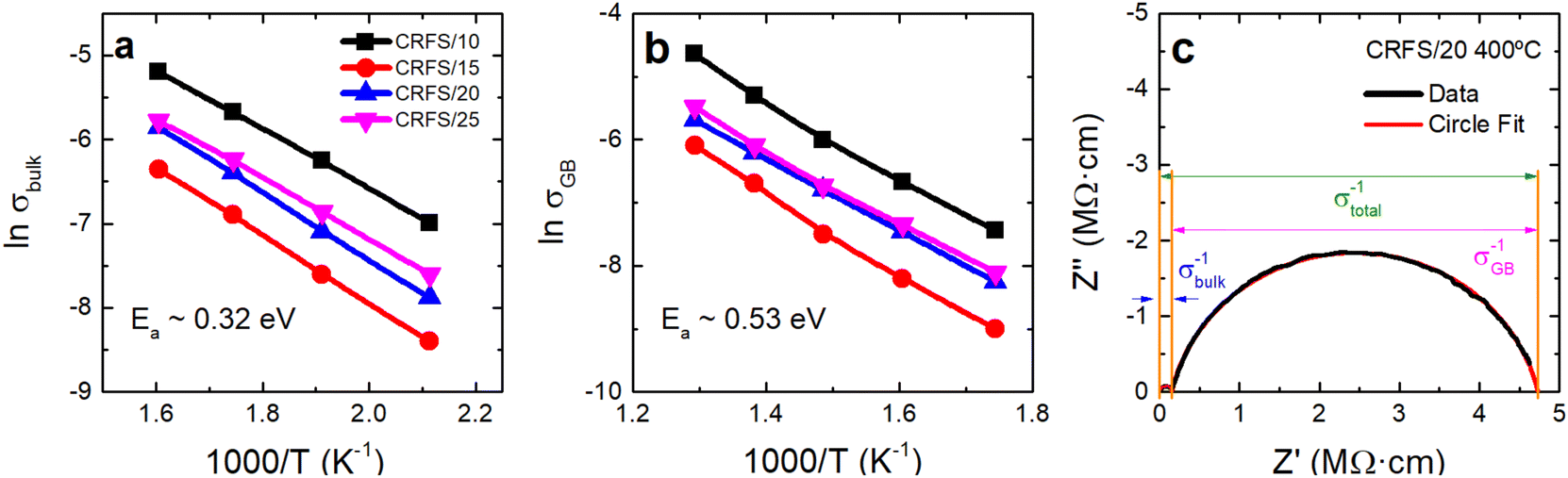 | ||
| Fig. 6 Impedance spectroscopy analysis of CRF-sintered Ba0.6Sr0.4TiO3 samples. Temperature dependence of (a) bulk and (b) grain boundary conductivities. (c) Z* plot for CRFS/20 sample at 400 °C. | ||
Arrhenius plots of bulk and grain boundary conductivity values, σbulk = 1/Rbulk and σGB = 1/RGB, extracted from the impedance complex plane plots over a range of temperatures for all samples are shown in Fig. 6a and b. Analysing the data obtained from the Arrhenius plots for the CRF-sintered samples, it is possible to notice a linear behaviour in all cases with similar activation energies, which suggests that the conduction mechanism is the same in all cases. Moreover, the effect of the CRFS conditions is evident; the Arrhenius plots of the sintered samples show significant differences in bulk and grain boundary resistivities depending on the sintering conditions. Specifically, the CRFS/15 sample shows higher bulk and grain boundary resistivities than the rest of the samples, which can be related with its particularly slim ferroelectric response.
Impedance spectroscopy is a powerful technique for distinguishing between the electrical responses of bulk and grain boundaries in ceramics. In this method, the electrical behaviour is often modelled using an equivalent circuit consisting of two parallel resistor–capacitor (RC) elements connected in series, representing bulk and grain boundary contributions. While impedance (Z*) plots in the complex plane (e.g., Z′′ vs. Z′) are commonly used, they can overemphasize the most resistive components, potentially obscuring regions with lower resistance. This limitation is particularly relevant for inhomogeneous ceramics. To gain a more comprehensive analysis and mitigate this issue, it is useful to present impedance data using at least two of the following four formalisms: impedance (Z*), admittance (Y*), permittivity (ε*), and electric modulus (M*). The interconversions between these formalisms can provide a more detailed understanding of the impedance characteristics.39 Each of these formalisms has real and imaginary components, such as Z* = Z′ − jZ′′.
Following these interconversions, data may be plotted as either complex plane plots, e.g. Z′′ vs. Z′ or as spectroscopic plots, e.g. Z′′ and M′′ vs. logf. When employing impedance spectroscopy to investigate electrical heterogeneity in ceramics, it is often more informative to use combined spectroscopic plots of Z′′ and M′′ rather than Z* plots. The M′′ spectra predominantly reflect electroactive regions with low capacitances, typically associated with grain-type responses. In contrast, Z′′ spectra (and Z* plots) are primarily influenced by the most resistive electroactive regions in the ceramic, such as grain boundary-type responses. Typically, each Debye peak observed in Z′′ and M′′ spectroscopic plots is initially interpreted as a parallel RC element. Thus, when multiple Debye peaks are present in the Z′′ and M′′ spectra, the data can be modelled using an equivalent circuit comprising two parallel RC elements connected in series.40
Spectroscopic plots of Z′′ and M′′ spectra at 450 °C for CRFS/15 is shown in Fig. 7a. M′′ plots identify those elements with the smallest capacitance since the M′′ peak maximum is equal to C0/2C, where C0 is the vacuum capacitance of the conductivity cell, without a sample in place. However, two peaks are observed in the M′′ spectrum, one not-well resolved at 300 Hz and a second, well resolved, at 355 kHz. The associated capacitance values of these peaks are ∼170 and ∼6 pFcm−1, respectively, and can be associated with the grain-boundary and bulk components. Impedance plots highlight the most resistive elements in the sample, since the impedance peak high, Z′′, is equal to R/2. Resistivities of ∼3.6 MΩ cm and ∼84 kΩ cm are obtained from the Z′′ spectroscopy plot for the low and high frequency components, respectively, and can be associated to the grain-boundary and bulk resistivities. It is important to mention that the M′′ spectrum does not show any further peaks or tails at high frequencies which could indicate bulk heterogeneity. Therefore, data can be interpreted on a series of two RC parallel elements attributed to the bulk and grain boundary. Only one peak is observed at lower and higher temperatures, corresponding to the bulk and grain boundary response, respectively. No other components are observed in the CRFS/15 sample.
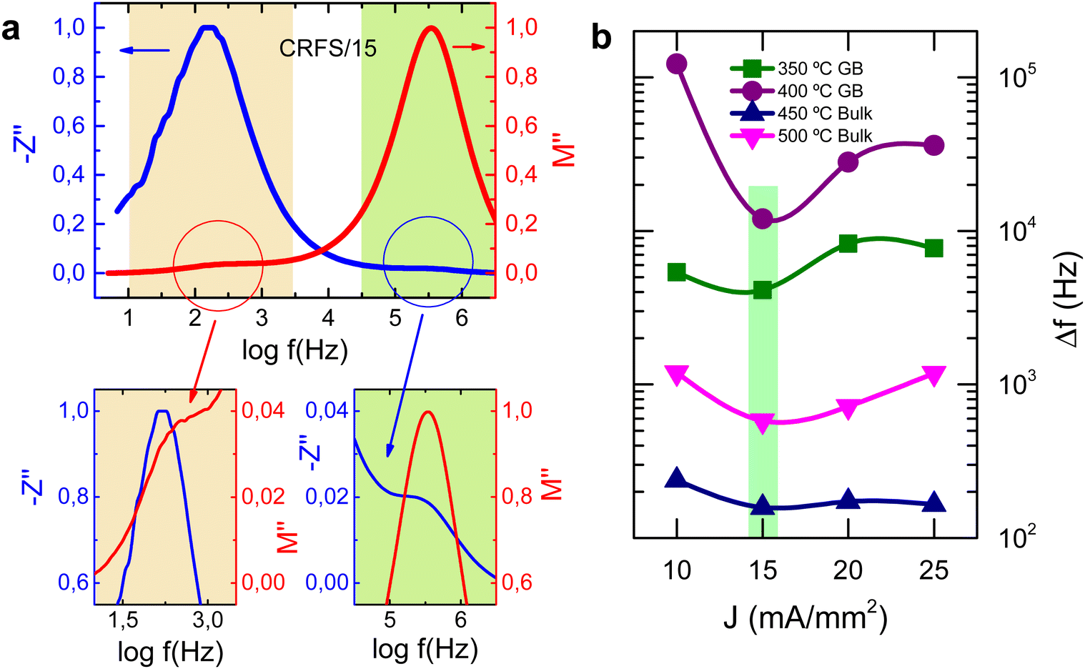 | ||
| Fig. 7 (a) Combined Z′′ and M′′ spectroscopic plots at 450 °C for CRFS/15 and (b) separation of M′′/Z′′ peak maxima for bulk and grain boundary peaks at different temperatures for all selected samples. The Z′′ and M′′ values are normalized for better visualization of the peak maxima in the combined plot. | ||
It is commonly observed a separation of M′′/Z′′ peak maxima which data may arise from non-ideal behaviour, as described by the constant phase element (CPE). However, it is critical to differentiate this effect from potential peak separation caused by sample heterogeneity.41 In order to determine whether the separation between M′′/Z′′ peak maxima, in both low and high frequency peaks, is a consequence of sample heterogeneity or a non-ideality, the peak difference was determined for all samples at different temperatures. As shown in Fig. 7b, the difference between the M′′ and Z′′ peak maxima are highly dependent on the sintering conditions. The CRFS/15 sample exhibits the smallest M′′/Z′′ peak difference across both low- and high-frequency regions and at various temperatures. In contrast, the other samples show larger peak differences, with the CRFS/10 sample displaying the largest deviation. To further highlight deviations from ideal behaviour and to identify overlapping peaks or weak signals that may be obscured on a linear scale, log−logplots of the M′′/Z′′ spectra for CRF-sintered samples at 300 °C, where only the bulk region is observed, are presented in Fig. 8. The CRFS/10, CRFS/20 and CRFS/25 samples (Fig. 8a, c and d) shows a broadening of the response at high frequencies in the M′′ spectroscopic plot. This behaviour strongly suggests some electrical heterogeneity within the grains of the CRFS/10, CRFS/20 and CRFS/25 samples. In contrast, the high-frequency region of the M′′ spectroscopic plot of the CRFS/15 sample (Fig. 8b) exhibits a behaviour that closely approximates Debye-like relaxation, indicating an electrically homogeneous grain response. The M′′/Z′′ spectra clearly indicate a substantial improvement in electrical homogeneity of the CRFS/15 sample compared to CRFS/10, CRFS/20 and CRFS/25 samples. This enhanced electrical homogeneity, coupled with higher resistivity, is more likely to foster enhanced energy storage properties.
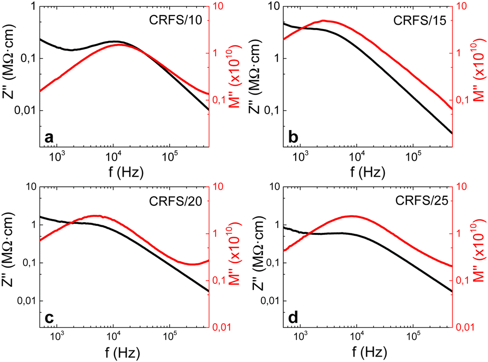 | ||
| Fig. 8 Spectroscopic plots of Z′′ and M′′ versus frequency on logarithmic scales for (a) CRFS/10, (b) CRFS/15, (c) CRFS/20, and (d) CRFS/25 samples at 300 °C. | ||
4 Conclusions
Highly-dense Ba0.6Sr0.4TiO3 ceramics are obtained by current-controlled reactive flash sintering of mixed BaTiO3–SrTiO3 powders. While current control may seem to increase the complexity of sintering by introducing additional parameters to manage, it proves to be an effective strategy for fine-tuning the microstructure. Moreover, current control in flash sintering is evidenced to provide a new pathway to precisely achieve a defect-engineered microstructure. High densification is achieved at a furnace temperature of 1200 °C with a dwell time of 5 min, showing notable differences in dielectric and ferroelectric properties depending on the current density, which ranges between 10–25 mA mm−2. These differences are revealed to be related to the microstructure, particularly the grain size distribution by volume.The sample with the most refined microstructure was characterized for energy storage applications. Despite the Ba0.6Sr0.4TiO3 composition being non-optimal for energy storage, the results demonstrated energy storage capabilities comparable to those reported for more tailored compositions in the literature. It is important to point out that the pursuit of exceptional properties for the Ba1−xSrxTiO3 system was not the goal of this work, as it is well-known that there are compositions that outperform Ba1−xSrxTiO3 for this application. The objective of this study is to demonstrate that microstructural refinement is a key tool for optimizing the performance of ferroelectric materials for energy storage. The studied composition was deliberately chosen outside the optimal range to make our demonstration even more evident.
The quality and electrical homogeneity of the flash-sintered samples were evaluated using impedance spectroscopy. The CRFS/15 sample exhibited higher bulk and grain boundary resistivities, as well as greater electrical homogeneity. These unique electrical properties are undoubtedly associated with its slim ferroelectric response and, consequently, its improved energy storage capability. This work highlights that microstructural refinement and, consequently, electrical homogeneity, are key factors in enhancing the energy storage capacity of ferroelectric materials.
Author contributions
Samuel Lopez-Blanco: conceptualization, methodology, formal analysis, investigation, writing – original draft; Xavier Vendrell: methodology, formal analysis, visualization, writing – review & editing; Nerea Morante: methodology, investigation; Jose E. Garcia: conceptualization, methodology, visualization, writing – review & editing, supervision, project administration.Data availability
All data included in this study will be made available upon request from the corresponding author.Conflicts of interest
There are no conflicts to declare.Acknowledgements
S. L.-B. thanks Agècia de Gestió d’Ajuts Universitaris i de Recerca (AGAUR), Catalonia, Spain, for the FI-SDUR contract (2020 FISDU 00489).References
- W. Kwestroo and H. A. M. Paping, J. Am. Ceram. Soc., 1959, 42, 292–299 Search PubMed.
- C. Zhao, Y. Huang and J. Wu, InfoMat, 2020, 2, 1163–1190 CrossRef CAS.
- Z. Li, J. Yu, S. Hao and P.-E. Janolin, J. Eur. Ceram. Soc., 2022, 42, 4693–4701 Search PubMed.
- V. V. Lemanov, E. P. Smirnova, P. P. Syrnikov and E. A. Tarakanov, Phys. Rev. B: Condens. Matter Mater. Phys., 1996, 54, 3151–3157 Search PubMed.
- S.-Y. Kuo, W.-Y. Liao and W.-F. Hsieh, Phys. Rev. B: Condens. Matter Mater. Phys., 2001, 64, 224103 Search PubMed.
- J. H. Yoo, W. Gao and K. H. Yoon, J. Mater. Sci., 1999, 34, 5361–5369 Search PubMed.
- B. Su and T. Button, J. Eur. Ceram. Soc., 2001, 21, 2641–2645 Search PubMed.
- B. Su, J. Holmes, C. Meggs and T. Button, J. Eur. Ceram. Soc., 2003, 23, 2699–2703 Search PubMed.
- G. Zhang, S. Jiang, Y. Zeng, Y. Zhang, Q. Zhang and Y. Yu, J. Am. Ceram. Soc., 2009, 92, 3132–3134 CrossRef CAS.
- L. P. Curecheriu, L. Mitoseriu and A. Ianculescu, J. Alloys Compd., 2009, 482, 1–4 Search PubMed.
- A. Jain, Y. Wang and L. Shi, J. Alloys Compd., 2022, 928, 167066 Search PubMed.
- N. H. Fletcher, A. D. Hilton and B. W. Ricketts, J. Phys. D: Appl. Phys., 1996, 29, 253 CrossRef CAS.
- T. Wu, Y. Pu, P. Gao and D. Liu, J. Mater. Sci.: Mater. Electron., 2013, 24, 4105–4112 CrossRef CAS.
- V. Veerapandiyan, F. Benes, T. Gindel and M. Deluca, Materials, 2020, 13, 5742 CrossRef CAS PubMed.
- G. Dong, S. Ma, J. Du and J. Cui, Ceram. Int., 2009, 35, 2069–2075 Search PubMed.
- T. Wang, L. Jin, L. Shu, Q. Hu and X. Wei, J. Alloys Compd., 2014, 617, 399–403 Search PubMed.
- Y. Wang, Z.-Y. Shen, Y.-M. Li, Z.-M. Wang, W.-Q. Luo and Y. Hong, Ceram. Int., 2015, 41, 8252–8256 CrossRef CAS.
- Y. H. Huang, Y. J. Wu, J. Li, B. Liu and X. M. Chen, J. Alloys Compd., 2017, 701, 439–446 Search PubMed.
- Y. J. Wu, Y. H. Huang, N. Wang, J. Li, M. S. Fu and X. M. Chen, J. Eur. Ceram. Soc., 2017, 37, 2099–2104 CrossRef CAS.
- Z. Song, H. Liu, S. Zhang, Z. Wang, Y. Shi, H. Hao, M. Cao, Z. Yao and Z. Yu, J. Eur. Ceram. Soc., 2014, 34, 1209–1217 Search PubMed.
- G. Wang, Z. Lu, Y. Li, L. Li, H. Ji, A. Feteira, D. Zhou, D. Wang, S. Zhang and I. M. Reaney, Chem. Rev., 2021, 121, 6124–6172 CrossRef CAS PubMed.
- Z. Yang, F. Gao, H. Du, L. Jin, L. Yan, Q. Hu, Y. Yu, S. Qu, X. Wei, Z. Xu and Y.-J. Wang, Nano Energy, 2019, 58, 768–777 Search PubMed.
- T. Hungría, M. Algueró, A. B. Hungría and A. Castro, Chem. Mater., 2005, 17, 6205–6212 Search PubMed.
- C. Mao, S. Yan, S. Cao, C. Yao, F. Cao, G. Wang, X. Dong, X. Hu and C. Yang, J. Eur. Ceram. Soc., 2014, 34, 2933–2939 Search PubMed.
- Y. Zhai, X. Xie, R. Zhou, X. Li, X. Liu and S. Liu, Ceram. Int., 2019, 45, 15526–15531 CrossRef CAS.
- C. Ribeiro, A. Tkach, F. Zorro, P. Ferreira, M. E. Costa and P. M. Vilarinho, J. Eur. Ceram. Soc., 2024, 44, 116761 CrossRef CAS.
- M. Biesuz and V. M. Sglavo, J. Eur. Ceram. Soc., 2019, 39, 115–143 Search PubMed.
- B. Yoon, V. Avila, I. R. Lavagnini, J. V. Campos and L. M. Jesus, Adv. Eng. Mater., 2023, 25, 2200731 CrossRef CAS.
- S. López-Blanco, D. A. Ochoa, X. Vendrell, L. Mestres and J. E. García, J. Eur. Ceram. Soc., 2022, 42, 5669–5674 Search PubMed.
- J. Luo, Scr. Mater., 2018, 146, 260–266 Search PubMed.
- H. Charalambous, S. K. Jha, K. H. Christian, R. T. Lay and T. Tsakalakos, J. Eur. Ceram. Soc., 2018, 38, 3689–3693 Search PubMed.
- P. Kumar MK, D. Yadav, J.-M. Lebrun and R. Raj, J. Am. Ceram. Soc., 2019, 102, 823–835 CrossRef CAS.
- I. R. Lavagnini, J. V. Campos, J. A. Ferreira and E. M. J. A. Pallone, J. Am. Ceram. Soc., 2020, 103, 3493–3499 Search PubMed.
- S. López-Blanco, D. A. Ochoa, H. Amorín, A. Castro, M. Algueró and J. E. García, J. Eur. Ceram. Soc., 2023, 43, 7440–7445 Search PubMed.
- S. López-Blanco, F. Rubio-Marcos, A. Barrón, D. A. Ochoa and J. E. García, J. Eur. Ceram. Soc., 2024, 44, 5702–5709 CrossRef.
- J. S. C. Francis and R. Raj, J. Am. Ceram. Soc., 2013, 96, 2754–2758 Search PubMed.
- L. Yang, X. Kong, F. Li, H. Hao, Z. Cheng, H. Liu, J.-F. Li and S. Zhang, Prog. Mater. Sci., 2019, 102, 72–108 CrossRef CAS.
- G. Wang, J. Li, X. Zhang, Z. Fan, F. Yang, A. Feteira, D. Zhou, D. C. Sinclair, T. Ma, X. Tan, D. Wang and I. M. Reaney, Energy Environ. Sci., 2019, 12, 582–588 RSC.
- J. T. S. Irvine, D. C. Sinclair and A. R. West, Adv. Mater., 1990, 2, 132–138 CrossRef CAS.
- E. Abram, D. Sinclair and A. West, J. Electroceram., 2003, 10, 165–177 CrossRef CAS.
- J. Ramírez-González, D. Sinclair and A. West, J. Electrochem. Soc., 2023, 170, 116504 CrossRef.
Footnote |
| † Electronic supplementary information (ESI) available. See DOI: https://doi.org/10.1039/d4tc04433a |
| This journal is © The Royal Society of Chemistry 2025 |