
 Open Access Article
 This Open Access Article is licensed under a Creative Commons Attribution-Non Commercial 3.0 Unported Licence
Multifunctional benzonitrile derivatives with TADF and mechanofluorochromic properties and their application in OLEDs†
Antonio
Maggiore
 *ab,
Yangyang
Qu
a,
Gilles
Clavier
a,
Marco
Colella
c,
Andrew
Danos
cd,
Andrew
Monkman
c,
Regis
Guillot
e,
Marco
Pugliese
b,
C. Tania
Prontera
b,
Roberto
Giannuzzi
b,
Fabrizio
Mariano
b,
Sonia
Carallo
b,
Gianluca
Accorsi
b,
Vincenzo
Maiorano
b,
Pierre
Audebert
a,
Remì
Metivier
a and
Fabien
Miomandre
a
*ab,
Yangyang
Qu
a,
Gilles
Clavier
a,
Marco
Colella
c,
Andrew
Danos
cd,
Andrew
Monkman
c,
Regis
Guillot
e,
Marco
Pugliese
b,
C. Tania
Prontera
b,
Roberto
Giannuzzi
b,
Fabrizio
Mariano
b,
Sonia
Carallo
b,
Gianluca
Accorsi
b,
Vincenzo
Maiorano
b,
Pierre
Audebert
a,
Remì
Metivier
a and
Fabien
Miomandre
a
aUniversité Paris-Saclay, ENS Paris-Saclay, CNRS, PPSM, Gif-sur-Yvette, 91190, France
bCNR-NANOTEC – Institute of Nanotechnology, c/o Campus Ecoteckne, Via Monteroni, Lecce, 73100, Italy. E-mail: antonio.maggiore@cnr.it
cDepartment of Physics, University of Durham, South Road, Durham, DH1 3LE, UK
dSchool of Physical and Chemical Sciences, Queen Mary University of London, London, E1 4NS, UK
eUniversité Paris-Saclay, CNRS, Institut de chimie moléculaire et des matériaux d’Orsay, Orsay, 91405, France
First published on 28th April 2025
Abstract
In this study, we explore the solid-state photophysical properties of four donor–acceptor–donor′ (D–A–D′) fluorinated benzonitrile compounds, featuring combinations of phenoxazine and carbazole donor units. We have previously shown that these compounds exhibit dual charge transfer thermally activated delayed fluorescence (CT-TADF) emission in solution; here we investigate the steady-state and time-resolved photophysical properties in the solid state. Initial photophysical characterizations were performed in polymethyl methacrylate (PMMA) polymer films, followed by detailed studies of the supramolecular packing in neat films under various preparation conditions, including solvent exposure and thermal treatments. Different polymorphs and amorphous phases were obtained, revealing that the dual TADF emission could be maintained to some extent in the solid-state. Mechanical stress and solvent vapour exposure induced mechanochromic luminescence (MCL), with emission changes correlating to the supramolecular structures. OLED devices were also fabricated, demonstrating similar tuneable emission properties based on preparation techniques. This work highlights the potential of this class of materials towards advanced optoelectronic applications with tuneable and stimuli-responsive emission characteristics.
1. Introduction
Organic semiconductor materials that efficiently harvest otherwise non-emissive triplet excitons are crucial for optoelectronic devices,1,2 such as organic light-emitting diodes (OLEDs) and organic photovoltaics (OPVs).3 To date, several strategies have been proposed to harvest triplet excitons, with the most promising based on thermally activated delayed fluorescence (TADF) emitters.4–7 These fully organic materials have attracted tremendous attention as they allow for the replacement of rare and/or toxic organometallic complexes traditionally used as phosphorescent emitting layers in OLED devices. Triplet harvesting in TADF materials is achieved by molecular designs that result in a very small singlet–triplet energy gap (ΔES–T), typically less than 0.1 eV and comparable to ambient thermal energy. This small gap allows triplet excitons to be upconverted back to the singlet via the reverse intersystem crossing (RISC) process, enabling emission. To reduce ΔES–T, it is necessary to minimize the spatial overlap between the highest occupied molecular orbital (HOMO) and the lowest unoccupied molecular orbital (LUMO).7 The most common strategy towards this end is to use donor–acceptor (D–A) or donor–acceptor–donor (D–A–D) designs, which promote the formation of strong charge transfer (CT) states.8 The HOMO/LUMO spatial separation can be further increased by using a phenyl linker as the spacer, or by tilting the D–A torsional angle to a nearly orthogonal configuration.9–11 This pre-twisted D–A configuration also helps to avoid tight packing and detrimental strong π–π interactions that favor non-radiative deactivation channels in the solid state.12,13 In addition, D–A and D–A–D luminescent organic materials, thanks to the presence of strong CT states, show a strong ability to change their optical output in response to environmental changes (e.g. solvent polarity, medium stiffness, etc.).14–17It has also been shown that D–A and D–A–D materials in the condensed phase can be highly sensitive to external stimuli such as grinding or pressing, exhibiting mechanochromic luminescence (MCL) behaviour, as well as heating and solvent exposure,18,19 all of which impact emission colour either by enacting conformational changes in the molecules or by altering intermolecular interactions between neighbouring molecules.20–23 Mechanochromic luminescence typically starts from a crystalline or aggregated phase that switches to another crystalline or amorphous phase after mechanical stress, with an accompanying change in the emission spectrum, this phenomenon being allowed by the polymorphism of the material. The search for polymorphic crystal forms of such emitters is widely investigated as it enables interesting properties and applications, especially in optoelectronics.24–27 The high sensitivity of some D–A materials to external stimuli, together with their ability to resist aggregation caused quenching (ACQ) phenomena, is driving research to develop new D–A materials with MCL properties,28–30 particularly for sensor development.
In the present work, we investigate the solid-state photophysical properties of a series of four donor–acceptor–donor′ (D–A–D′) fluorinated benzonitrile (BzN, A) compounds (Fig. 1a) substituted with mixed phenoxazine (PhOx) and carbazole (Cz) donor units (D and D′). We have previously shown that these compounds exhibit dual CT-TADF emission in solution, from excited states involving Cz and PhOx.31 In this study, we have investigated in detail the steady-state and time-resolved photophysical properties in polymethylmethacrylate (PMMA) rigid films, as well as in the non-doped condensed phase. We have specifically studied the supramolecular packing obtained in neat films by varying the sample preparation conditions (e.g. type of solvent, solvent saturation conditions and temperature; see the ESI† for more details). This allows us to obtain different polymorphs or amorphous phases with various MCL properties that also translate to OLED emission in non-doped emissive layers.
 | ||
| Fig. 1 (a) Molecular structures of the molecules studied. (b) Normalized photoluminescence spectra of 4–7 in cyclohexane (10−5 M). Inset: Normalized photoluminescence spectra of 4–7 in cyclohexane (10−5 M) excited on the lower energy CT band, λexc = 390–450 nm. (c) Normalized photoluminescence spectra of 4–7 in PMMA. | ||
2. Results and discussion
2.1. Steady-state PL of the isolated molecule in dilute solution and polymer matrix
The steady state emission properties of isolated molecules 4–7, both in solution and within a rigid polymer matrix, have been previously reported.31 We retain the molecular naming conventions from this previous work to enable straightforward comparisons here, and briefly summarize the PL in cyclohexane (CH) and in the rigid polymer environment (PMMA) (Fig. 1). In solution, dual emission is evident when the molecule is excited at the locally excited (LE) absorption band (higher energy) (Fig. 1b). However, when excited at the lower energy CT absorption band (Fig. S12, ESI†), only a single emission band remains (inset, Fig. 1b). In contrast, in PMMA, the higher energy band appears weak and diminishes further with an increasing number of carbazole (Cz) units. As discussed previously,31 for compounds 4 and 5, the higher energy emission is attributed to the sum of both LE from PhOx and CT involving Cz contributions. For compounds 6 and 7 it is attributed exclusively to Cz CT. The lower energy band for all compounds is assigned to the CT state involving phenoxazine (PhOx CT).31 From the inset of Fig. 1b, we can observe a slight red shift of the emission, particularly at the onset, with an increasing number of carbazole units. This behaviour is more pronounced in PMMA (Fig. 1c), indicating that the number of Cz units also influences the CT involving phenoxazine. The different behaviour observed in the solid environment is likely due to the restricted rotation of carbazole in the solid state compared to the solution, which prevents the stabilization of the Cz CT state.32 As a result, most of the energy is directed towards the PhOx CT through internal conversion processes.2.2. Study in the condensed phase
Here we report the photophysical properties and XRD analysis of the condensed phase samples. We begin by describing the various sample preparation techniques used to control the supramolecular arrangement of the studied materials. All samples with the corresponding preparation techniques are summarized in Table 1.| Molecule | Sample name | Preparation technique |
|---|---|---|
| 4 | 4fDCM | Drop casting from DCM |
| 4fSVA | Solvent vapour annealing | |
| 4fDCM150 | Drop casting from DCM + 150 °C | |
| 4fTOL | Drop casting from toluene | |
| 5 | 5fDCM | Drop casting from DCM |
| 5fSVA | Solvent vapour annealing | |
| 5fDCM150 | Drop casting from DCM + 150 °C | |
| 5fTOL | Drop casting from toluene | |
| 6 | 6fDCM | Drop casting from DCM |
| 6fSVA | Solvent vapour annealing | |
| 6fDCM150 | Drop casting from DCM + 150 °C | |
| 6FDCM200 | Drop casting from DCM + 200 °C | |
| 6fTOL | Drop casting from toluene | |
| 7 | 7fDCM | Drop casting from DCM |
| 7fSVA | Solvent vapour annealing | |
| 7fDCM150 | Drop casting from DCM + 150 °C | |
| 7fTOL | Drop casting from Toluene | |
To prepare the different neat (non-doped) films, we varied the chemical and physical processing conditions such as solvent polarity, temperature and evaporation rate (see the ESI† for more details). Fast solvent evaporation (conducted under a hood) resulted in amorphous films, while slower, controlled evaporation (achieved by saturating the evaporation chamber with the solvent) generally resulted in more ordered or crystalline phases. Specifically:
– Solvent vapour annealing (SVA) is a slow evaporation process where the solvent vapor environment promotes molecular mobility, favouring self-assembly and crystallization.33 The samples obtained by solvent vapour annealing (using as a solvent toluene into a hexane saturated chamber, see the ESI† for details) of particular emitter “X” are labelled as “XfSVA”, (f = from).
– Dropping the solution directly onto the substrate enables us to control the assembly by selecting appropriate solvents. We used two different solvents: DCM (dichloromethane), which has a low boiling point and fast evaporation properties, favouring an amorphous phase, and toluene, which has a high boiling point and high viscosity, favouring high-order molecular self-assembly. The samples obtained by drop casting with DCM are labelled with postscript fDCM, and those from toluene with fTOL.
– In addition, we also used thermal annealing, which facilitates molecular diffusion and nucleation, leading to crystalline phases following initial deposition. This was achieved by heating the drop cast samples from the DCM solution at 150 °C or 200 °C for 15 minutes. The samples obtained by thermally annealing are labelled as fDCM150 (T = 150 °C) and fDCM200 (T = 200 °C).
Images of all prepared samples are shown in the ESI† (Fig. S1–S4).
 | ||
| Fig. 2 Powder XRD patterns of different forms of the reported molecules: (a) molecule 4, (b) molecule 5, (c) molecule 6, and (d) molecule 7. | ||
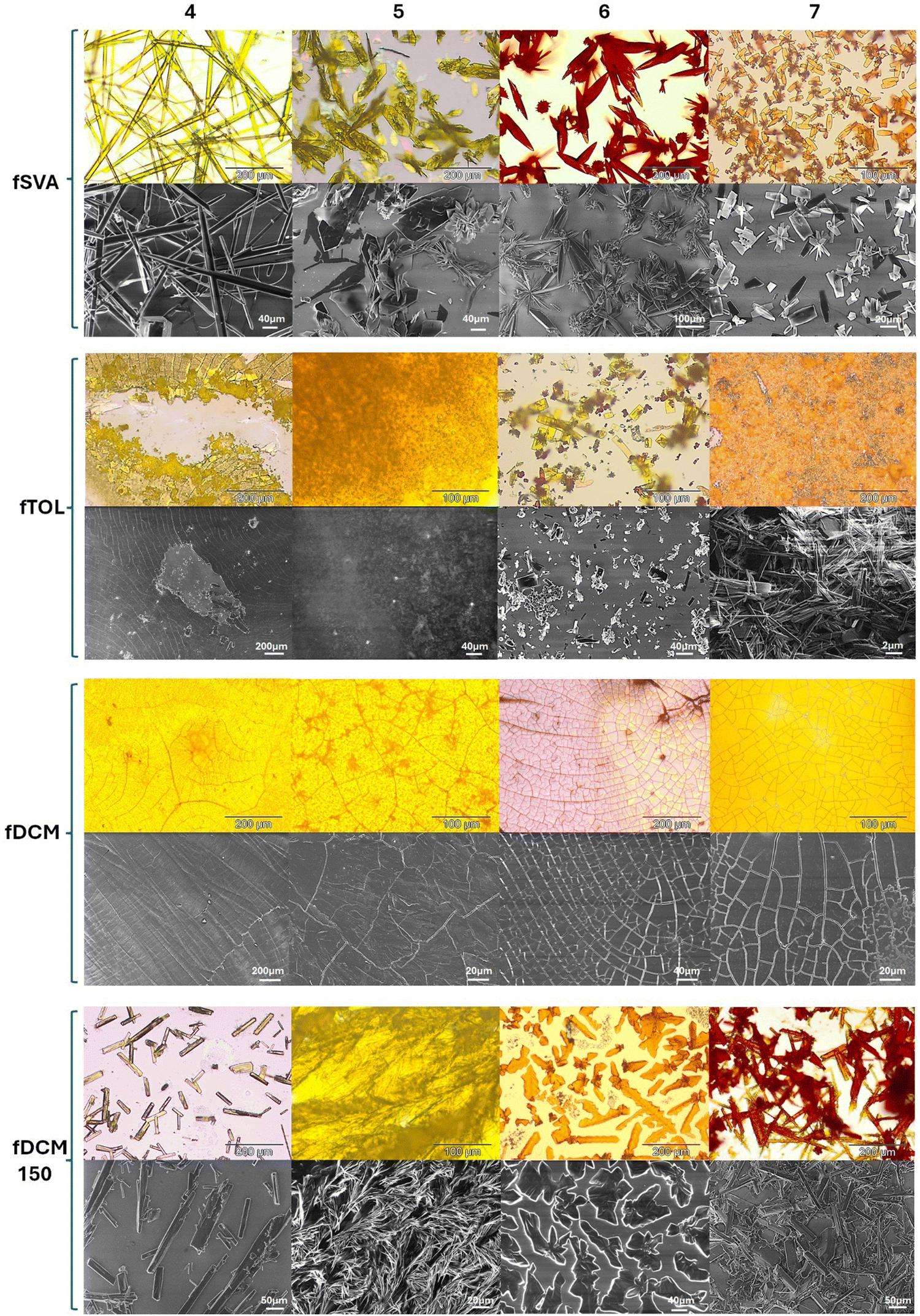 | ||
| Fig. 3 Surface morphology of samples 4–7 prepared using the different processing methods (fDCM, fTOL, fSVA, and fDCM150). Top panels (colour images) show optical microscopy photographs. Bottom panels (black and white images) display the corresponding scanning electron microscopy (SEM) images. The images revealing microscale surface features and morphological variations induced by the preparation methods. Scale bars are included in all optical and SEM images. | ||
All films prepared via solvent vapor annealing (fSVA) and thermal annealing at 150–200 °C display distinct diffraction peaks, confirming the presence of crystalline phases. Similarly, all fTOL samples exhibit crystalline features, with the exception of 5fTOL. In contrast, fDCM films are X-ray amorphous, consistent with the rapid solvent evaporation hindering molecular organization. Notably, variations in XRD patterns across different processing methods for the same molecule indicate polymorphism or variations in molecular packing driven by distinct crystallization dynamics. Single-crystal X-ray diffraction was also performed on crystals obtained from the initial powders (used for the MCL study in Section 5). For molecule 5, the unit cell contains two distinct molecules and one solvent molecule with different donor–acceptor (D–A) angles, consistent with the presence of multiple charge-transfer (CT) states (Table S1, ESI†). Two polymorphic forms were identified for molecule 6, one solvent-free and one solvated (6 and 6+solv), supporting the hypothesis that polymorphism plays a key role in modulating solid-state emission properties (Table S1, ESI†). Molecular packing in the single crystals of compounds 4–7 is illustrated in Fig. S5–S10 (ESI†). Key intermolecular interactions include C–H⋯π, C–H⋯N, C–F⋯H, C–H⋯O, and C–F⋯C. Notably, π–π stacking is observed only for compound 5 (offset stacking between two carbazole units with a π–π distance of 3.702 Å; Fig. S5b and S7, ESI†) and for 6+solv (offset, head-to-tail stacking between carbazoles with a distance of 3.867 Å; Fig. S5d and S9, ESI†). The presence of multiple donor groups and relatively weak directional interactions appears to facilitate conformational adaptability and structural rearrangement, consistent with the MCL behaviour observed in these systems.34–36
Optical and SEM images (Fig. 3 and Fig. S11, ESI†) corroborate the structural data obtained from XRD. Films obtained viafSVA show well-defined surface textures, with crystalline domains clearly observable under both optical and electron microscopy. The fTOL samples, excluding 5fTOL, also display heterogeneous morphologies, characterized by visible crystalline regions. For instance, 4fTOL features faceted multidomain sheets, while 6fTOL exhibits rectangular, flat crystalline domains. In 7fTOL, SEM reveals micrometric, filament-like aggregates not easily detected in optical images. In contrast, fDCM samples appear smooth and homogeneous in both optical and SEM analysis, reflecting their amorphous nature as confirmed by XRD. Similarly, 5fTOL presents a featureless morphology, consistent with its amorphous character. Upon thermal annealing of fDCM films, the formation of crystalline domains becomes evident. Optical and SEM images reveal the emergence of textured crystalline regions in 4fDCM150, 6fDCM150, 6fDCM200, and 7fDCM150. Interestingly, while 5fDCM150 appears featureless in optical microscopy, SEM at 20 μm resolution reveals branched crystalline domains. At higher magnification (4 μm), these appear as elongated, bar-like or rod-like structures (Fig. S11, ESI†).
Comparative analysis of the crystalline morphologies across different preparation methods provides further insight highlighting the sensitivity of molecular organization to processing conditions. Molecule 4 forms elongated, interconnected needle-like crystalline domains in fSVA. In 4fTOL, the crystals appear as large, flat, multifaceted domains with irregular polygonal boundaries. 4fDCM150 exhibits smaller, elongated rectangular flat domains. Molecule 5 forms elongated hexagonal platelets domains in fSVA, characterized by sharp edges and well-defined facets. 5fDCM150 displays a heterogeneous morphology; high-magnification SEM reveals small crystallites with bar-like or branched structures radiating from localized nucleation points (4 μm scale, Fig. S11, ESI†). For molecule 6, fSVA induces elongated spear-like crystallites. 6fTOL shows smaller rectangular faceted crystalline domains, while 6fDCM150 presents a polycrystalline mosaic texture. Upon annealing at 200 °C (6fDCM200), a clear morphological transition occurs, showing interconnected crystalline areas with petal-like features. Molecule 7 displays elongated hexagonal crystalline facets in fSVA. SEM images of 7fTOL reveal fibrous or needle-like crystalline structures. In 7fDCM150, SEM analysis shows parallelogram-shaped crystalline domains.
The combined XRD and microscopy analyses clearly demonstrate that the processing method strongly influences the crystallinity, molecular packing, and surface morphology of 4–7 thin films. The ability of each molecule to adopt multiple packing arrangements under different conditions is closely related to its polymorphic behaviour and is directly linked to the solid-state photophysical properties explored in subsequent sections.
 | ||
| Fig. 4 Normalized fluorescence spectra (λexc = 400 nm) of the different solid forms obtained for (a) molecule 4, (b) molecule 5, (c) molecule 6, and (d) molecule 7. | ||
| Comp. | QY (%) air | λ PL (nm) Std. state | FWHM (nm) | Emission onset (eV) | Excitation onset (eV) |
|---|---|---|---|---|---|
| 4SVA | 9.0 | 561 | 112 | 2.51 | 2.36 |
| 4fDCM150 | 3.3 | 573 | 124 | 2.43 | 2.32 |
| 4fTOL | 2.7 | 573 | 128 | 2.47 | 2.38 |
| 4fDCM | 1.0 | 594 | 141 | 2.46 | 2.31 |
| 5SVA | 7.8 | 567 | 112 | 2.47 | 2.36 |
| 5fDCM150 | 4.1 | 574 | 121 | 2.47 | 2.37 |
| 5fTOL | 1.1 | 610 | 140 | 2.44 | 2.35 |
| 5fDCM | 1.0 | 612 | 149 | 2.44 | 2.34 |
| 6SVA | 2.4 | 626 | 113 | 2.19 | 2.07 |
| 6fDCM150 | 7.3 | 598 | 123 | 2.35 | 2.31 |
| 6fDCM200 | 2.9 | 621 | 125 | 2.25 | 2.16 |
| 6fTOL | 2.6 | 598 | 116 | 2.33 | 2.15 |
| 6fDCM | 2.3 | 612 | 132 | 2.36 | 2.35 |
| 7SVA | 8.5 | 600 | 104 | 2.29 | 2.16 |
| 7fDCM150 | 2.8 | 613 | 124 | 2.29 | 2.13 |
| 7fTOL | 9.1 | 585 | 115 | 2.38 | 2.25 |
| 7fDCM | 1.8 | 620 | 131 | 2.31 | 2.21 |
Notably, each polymorph of compounds 6 and 7 (isolated in the XRD analysis) shows different photophysical behaviour. The emission at the highest energy is observed for 6fDCM150, which also exhibits CIEE properties (Table 2 and Fig. S13a, ESI†). In contrast the emission at lowest energy is detected for 6fSVA, which has the lowest QY in agreement with the energy gap law (Table 2 and Fig. S13a, ESI†). Interestingly, the crystalline 6fSVA film shows a bathochromic shift relative to the amorphous 6fDCM (Fig. S13a and b, ESI†), indicating that this molecular packing strongly stabilizes the CT state, leading to increased non-radiative deactivation paths. Conversely, 7fTOL shows a hypsochromic shift with higher PLQY relative to 7fSVA (Table 2 and Fig. S13a, ESI†). Looking at the different solid samples obtained from the same molecule, it can be seen that the bluer shifted the emission, the higher the QY (Table 2 and Fig. S13, ESI†). This behaviour is also valid for the polymorphs in 7fTOL/7fSVA and 6fDCM150/6fSVA.
Fig. S14 (ESI†) shows the absorption and excitation (PE) spectra of 4–7 in PMMA, and their good match indicates that all transitions involved in the absorption process contribute to the emission output. As previously discussed for the absorption in PMMA, the bands at lower energy are assigned to the CT transitions of PhOx–BzN (CT1) and Cz–BzN (CT2) moieties. Fig. S15 (ESI†) instead shows the PE spectra of all neat films, compared as well to PMMA, while those in Table S3 (ESI†) are reported for their peak maxima (λmax) and the onset for the lower energy bands. We can observe that for all molecules the higher energy peaks (between 363 and 367 nm), are intense and match with both the absorption and PE spectra of 4–7 in PMMA (Fig. S14, ESI†), and thus are assigned to the locally excited state of the donors. On the other hand, in neat films the CT1 and CT2 bands are strongly red-shifted and in most cases are also more intense compared to the isolated molecules in PMMA (Fig. S15 and Table S3, ESI†). Since no short distance π–π interactions were found (only long-distance π–π interactions between two carbazoles were found in 5 and 6+solv crystals Fig. S7 and S9, ESI†), the formation of aggregate emissive species is not orderly in these films. Therefore, the strong red-shift in the CT transitions observed in PE spectra can be attributed to either the presence of different molecular conformations in the solid samples and/or to different polarity and dielectric constants in the solid phases. These factors can produce a redistribution of the electronic density of the molecules that stabilizes the CT states.
2.3. Time-resolved photophysical properties
 | ||
| Fig. 5 Normalized time-resolved emission spectra of 4–7 in PMMA at room temperature (RT). | ||
The decay profiles of all compounds at RT in PMMA are shown in Fig. S20 (ESI†), and the decay times of other films (decays in Fig. S22–S36, ESI†) are summarized in Table 3. The prompt fluorescence (PF) part of the decay (nanosecond domain) is fitted with a biexponential function, with the two components associated with PF emission from the 1LE of PhOx and/or the 1CT of BzN–Cz. Similarly, the long-lived component (DF domain) also shows biexponential behavior, but in this case, the two decay times can be attributed to DF arising from the two CT states associated with the PhOx–BzN and Cz–BzN moieties. The power law relationship between DF emission intensity and excitation dose with gradient close to 1 confirms a monomolecular process for all compounds, excluding TTA as the DF mechanism (Fig. S17, S37–S40, ESI†). Both the time-resolved PL emission and decay profiles at RT show that, similar to the solution phase, dual TADF emission channels are present in the solid-state environment. However, the higher energy DF (originating from the Cz–BzN branch) contributes negligibly to the total emission output.
| λ std.st. (nm) | λ PF (nm) | S1onset (eV) | τ 1 (ns) | τ 2 (μs) | τ 3 (μs) | τ 4 (μs) | τ DF,av | QY (%) | DF/PF | |
|---|---|---|---|---|---|---|---|---|---|---|
| λ std.st. = emission maximum of steady-state fluorescence, λPF = emission maximum of prompt fluorescence, S1onset = onset energy of singlet, τPF,av = average decay time of PF, τDF,av = average decay time of DF, *: monoexponential, DF/PF= ratio between DF to PF emission. | ||||||||||
| 4fDCM | 594 | 605 | 2.41 | 2.2 | 0.3 | 0.9 | 4.0 | 1.3 | 1.0 | 0.03 |
| 4fTOL | 573 | 602 | 2.43 | 2.6 | 0.1 | 1.2 | — | 0.9 | 2.7 | 0.05 |
| 4fDCM150 | 573 | 560 | 2.43 | 4.0 | 1.4 | — | — | 1.4* | 3.3 | 0.09 |
| 4fSVA | 561 | 573 | 2.38 | 4.0 | 1.2 | — | — | 1.2* | 9.0 | 0.08 |
| 5fDCM | 612 | 600 | 2.36 | 2.2 | 0.2 | 0.8 | 3.7 | 1.4 | 1.0 | 0.17 |
| 5fTOL | 610 | 585 | 2.40 | 2.0 | 0.1 | 0.6 | 2.6 | 1.2 | 1.1 | 0.07 |
| 5fDCM150 | 574 | 562 | 2.46 | 4.6 | 0.4 | 2.8 | — | 2.2 | 4.1 | 0.15 |
| 5fSVA | 567 | 562 | 2.44 | 8.7 | 0.7 | — | — | 0.7* | 7.8 | 0.22 |
| 6fDCM | 612 | 609 | 2.28 | 3.1 | 0.2 | 1.3 | 4.4 | 1.3 | 2.3 | 0.05 |
| 6fDCM150 | 598 | 579 | 2.37 | 4.3 | 2.5 | — | — | 2.5* | 7.3 | 0.06 |
| 6fDCM200 | 621 | 612 | 2.21 | 3.3 | 1.0 | — | — | 1.0* | 2.9 | 0.04 |
| 6fSVA | 626 | 614 | 2.19 | 3.1 | 1.1 | — | — | 1.1* | 2.4 | 0.04 |
| 7fDCM | 620 | 611 | 2.30 | 2.2 | 0.03 | 0.3 | 2.0 | 1.6 | 1.8 | 0.05 |
| 7fSVA | 600 | 577 | 2.35 | 4.6 | 0.3 | 4.9 | — | 4.2 | 8.5 | 0.16 |
| 7fTOL | 585 | 574 | 2.39 | 5.2 | 0.3 | 5.6 | — | 4.7 | 9.1 | 0.26 |
Time-resolved emission was also collected at 77 K (Fig. S18, ESI†). Similar to RT, at initial times (nanosecond range), the time-resolved PL emission shows a shoulder/band at higher energy (450 nm) attributed to the PF of the 1LE of PhOx and/or the 1CT of BzN–Cz, and a main band at lower energy attributed to the 1CT PF of the PhOx–BzN moieties. With increasing delay time, the emission progressively redshifts and after 100 ns the shoulder at 450 nm disappears, leaving only a DF emission from the 1CT of the PhOx–BzN moiety. With further increasing the delay time, the emission progressively blue shifts and in some cases gains structural features, and since the late emission (TD = 70 ms) has an onset close to the phosphorescence of phenoxazine (Fig. S19, ESI†), it can be attributed to the emission from the phenoxazine fragment 3LE.
In conclusion, the time-resolved study in polymer shows that the dual TADF emission previously shown in solution remains present in the solid state. However, the higher energy DF emission (originating from the Cz–BzN branch) contributes negligibly to the total emission.
From the time-resolved spectra, it is evident that all samples exhibit typical TADF behaviour. However, while the emission in crystalline samples remains unchanged at different delay times (4fDCM150, 4fSVA, 5fDCM150, 5fSVA, 6fDCM150, 6fDCM200, 6fSVA, 7fTOL, 7fSVA), the amorphous samples show slight spectral evolution over time (4fDCM, 4fTOL, 5fDCM, 5fTOL, 6fDCM, and 7fDCM). Consequently, the amorphous films are fitted with bi- or multi-exponential curves, while the crystalline ones, with few exceptions, are fitted with mono-exponential curves. The laser fluency experiments reported in Fig. S37–S40 (ESI†) again show the expected linear dependence of the DF intensity on the laser power. Based on these observations, we can conclude that the dual emission observed in solution and in the polymer matrix is not as strongly maintained in the non-doped condensed phase. The double exponential decay observed in the amorphous samples is probably caused by the poor homogeneity of the films, which contain molecules with slightly different configurations. In contrast, the ordered packing of crystalline films allows only one molecular conformation to dominate.
2.4. OLED devices
To demonstrate the possibility of using this class of compound as emitting materials in an electroluminescent device, we fabricated OLEDs with the materials 4, 5, 6 and 7 as emitting layers (EMLs). The compounds were dispersed at 20% w/w in an appropriate host matrix (1,3-bis(N-carbazolyl)benzene, mCP), and the device′s structure was as follow: ITO/Pedot:PSS (35 nm)/PVK (10 nm)/mCP:compound 4–7 20% w/w (30 nm)/TPBI (50 nm)/LiF (1 nm)/Al (100 nm). We also fabricated OLEDs using thin neat films (100%) of the materials 4, 5, 6 and 7 as emitting layers (EMLs), testing the effect of annealing on the EMLs in order to evaluate how the supramolecular packing can influence the electroluminescence properties.The results of electro-optical characterization of the OLEDs are shown in Fig. 6. As expected, devices using a host:guest system as EML perform better than the neat film case. In particular, devices with molecules 4, 5, 6 and 7 dispersed in mCP show a maximum current efficiency of 2.8, 3.4, 6.4 and 7.6 cd A−1, respectively, with luminance that in any case exceeds 1000 cd m−2. Conversely, self-quenching induces detrimental effects on neat film-based devices, for which the performance drops considerably, both in terms of efficiency and luminance. This behaviour is even more evident if the neat film EMLs are annealed after deposition. In that case, although the quantum yield is higher in modified films than in amorphous films (Table 2), we found that OLEDs exposed to the annealing step (and thus also exhibiting aggregation/crystallisation in the EML) generally have much lower efficiencies (see Fig. 6). This may be due to alterations in the morphology of the active layer as a result of heat exposure and the induced supramolecular organisation, which negatively impacts the electrical characteristics of the devices to a greater extent than any increase in PLQY. This also emerges from the current density curves as a function of the applied voltage, where it is clear that in the case of devices with an annealed EML there is a significant increase in passive currents even at low voltage. The external quantum efficiency (EQE) has been estimated for all OLEDs and is shown in Fig. S41 (ESI†).
 | ||
| Fig. 6 Electroluminescent characteristics of OLEDs using 4, 5, 6 and 7 as the active layer, dispersed in an appropriate matrix (mCP) and in neat film (with or without annealing). Voltage vs. current density, voltage vs. luminance and voltage vs. efficiency for molecules 4 (a)–(c), 5 (d)–(f), 6 (g)–(i) and 7 (j)–(l). | ||
We then compared the electroluminescence spectra of the devices with an EML in neat film (Fig. 7), with and without thermal annealing. The latter was used to induce/accelerate an eventual transition from the amorphous phase of the film to an aggregate/crystalline phase, as was observed in optical studies of the corresponding films. In all devices exposed to annealing at 150 °C, a shift of the emission towards higher energies can be observed, compared to the spectra of the non-annealed devices. The shift is in line with that observed in the steady-state photoluminescence spectra (Table 2) and suggests the formation of aggregates or crystalline domains whose optical properties are also reflected in electroluminescence.
 | ||
| Fig. 7 Comparison between normalized electroluminescence and photoluminescence spectra using: (a) compound 4; (b) compound 5; (c) compound 6; (d) compound 7, before and after thermal annealing. | ||
2.5. MCL study
Building on the observation that these materials can form optically and structurally distinct solid-state phases depending on the processing conditions, we also tested explicitly their MCL properties. All MCL studies were performed using the setup described in the ESI† (Fig. S42). Initial powders of 4–7 obtained from the synthesis appeared visually as either multicrystalline, or amorphous (Fig. S43–S46, ESI†). Firstly, these starting powders were subjected to mechanical stress (Fig. 8 and Fig. S47, ESI†) by grinding the materials with a pestle in a mortar. The powders were then exposed to vapours of DCM and toluene (in the order shown in Fig. 8 and Fig. S47, ESI†). To compare the different forms obtained in the films with the phases obtained in the MCL study, Table 4 reports the emission maxima for the MCL study, while Table S5 (ESI†) shows the PL λmax of the neat films. Table S5 (ESI†) also compares the PL obtained with the MCL setup to that obtained with the spectrofluorometer. It should be noted that the slight spectral shift in the latter case is due to the correction applied to the detector response, leaving the two setups still comparable. | ||
| Fig. 8 MCL study for molecules 4, 6 and 7: (a) photographs of various forms obtained during the MCL study (the photographs were taken at 365 nm excitation); (b) PL spectra of the various forms of 4 studied in MCL, and PL spectra of 4fSVA obtained with the MCL setup. (c) PL spectra of the various forms of 6 studied in MCL, and PL spectra of 6fDCM150 and 6fDCM obtained with the MCL setup. (d) PL spectra of the various forms of 7 studied in MCL, and PL spectra of 7fSVA, 7fDCM and 7fTOL obtained with the MCL setup. (Gr.: grinding; +TOL: exposition to toluene; +DCM: exposition to DCM). | ||
| (Initial)aλPL, nm | +GrindingbλPL, nm | +DCM vapourcλPL, nm | +Grinding λPL, nm | +TOL vapourdλPL, nm | +Grinding λPL, nm | |
|---|---|---|---|---|---|---|
| a Initial powder. b Grinding in the mortar. c Exposure to DCM vapour. d Exposure to Toluene vapour. | ||||||
| 4 cryst. powd. | 577 | #1, 586 | 608 | — | 582 | 601 |
| #2, 599 | ||||||
| 5 cryst. powd. | 578 | 603 | 608 | — | 608 | — |
| 6 cryst-red powd. | 629 | 611 | 610 | — | 609 | — |
| 6 orange cryst | 610 | 601 | — | — | 578 | 610 |
| 7 crystal | 602 | 624 | — | — | — | — |
| 7 red powder | 621 | 621 | 621 | 621 | 592 | 621 |
The initial crystalline powders of compounds 4 (Fig. 8) and 5§ (Fig. S47, ESI†) show a bright yellow emission similar to that of 4fSVA and 5fSVA. Upon grinding, the emission shifts to red and its brightness decreases, resulting in spectra similar to those of 4fDCM and 5fDCM, indicating the formation of amorphous phases also in the powders. The ground powders of 4 and 5 were then exposed to DCM vapours (+DCM), resulting in a slight red shift of the emission. Subsequent exposure to toluene vapours (+TOL) caused the emission to return to the initial position, similar to that of 4fTOL, indicating the restoration of the crystalline form. However, no spectral shift was observed when 5 (+DCM) was exposed to toluene (+TOL) (Fig. S47, ESI†), consistent with the behaviour of 5fTOL.
Two different forms of compound 6 were observed in the initial powder precipitated from the same batch (Fig. S45, ESI†). One form appeared as a polycrystalline red powder (Fig. S45 and S47, ESI†) with a narrow emission (λmax = 629 nm) similar to both 6fSVA and 6fDCM200 (steady state). The other form appeared as an orange crystal (λmax = 610 nm) (Fig. 8 and Fig. S45, circled, ESI†). These two forms were manually separated with a pair of tweezers. Grinding of the polycrystalline red powder resulted in a broadened and blue-shifted emission (18 nm), indicating the formation of an amorphous phase with emission similar to that of 6fDCM. Grinding of the orange crystals (Fig. 8) resulted in a blue shift (9 nm) together with broadening of the emission. The compound remained crystalline as indicated by the emission matching with 6fDCM150 (Fig. 8c). Finally, exposure of the ground orange crystal to toluene resulted in a hypsochromic shift (23 nm) with a narrowed yellow emission, different from that observed for the drop-cast thin films, indicating the formation of a possible additional polymorph that red-shifts upon grinding.
The initial powder of compound 7 also presented two different forms (Fig. S46, ESI†): one as a multicrystalline orange powder (λmax = 601 nm, Fig. S47, ESI†) and the other as a red powder (λmax = 621 nm, Fig. 7). Grinding the multicrystalline orange powder (similar emission to 7fSVA, Fig. S47, ESI†) resulted in a red-shifted emission similar to 7fDCM, indicating the formation of the amorphous phase. Grinding the red powder (Fig. 8) resulted in a blue-shift of the emission onset, which becomes broader and similar to that of 7fDCM, indicating that the initial powder contained a more ordered phase. Exposure of the ground powder to DCM did not change the emission, consistent with an amorphous material. Finally, exposure to toluene favoured crystallisation, as indicated by the strong blue shift (λmax = 592 nm), matching that of 7fTOL. A second grinding redshifted the emission back to the amorphous phase.
Overall, the MCL behaviour observed for compounds 4–7 can be rationalized by considering both intramolecular conformational flexibility and supramolecular organization, as revealed by single-crystal XRD, thin-film XRD, and SEM analyses. The D–A torsion angles extracted from the single-crystal data (Table S1, ESI†) vary between polymorphs and influence the electronic coupling between donor and acceptor moieties, thus modulating the energy and efficiency of the CT excited states. Crystalline samples such as fSVA derivatives (excluding 6fSVA), 6fDCM150, and 7fTOL exhibit blue-shifted, narrower, and more intense emission consistent with more twisted D–A conformations and reduced non-radiative decay. This behaviour is likely due to conformational locking and restricted relaxation pathways in ordered molecular environments. In contrast, red-shifted and broader emission with lower PLQYs, as observed for 6fSVA, 6fDCM200, 5fTOL, and the amorphous fDCM samples, is indicative of more planar D–A conformations and enhanced CT stabilization. While in amorphous films this behaviour is likely due to increased conformational freedom, in crystalline samples such as 6fSVA and 6fDCM200, it likely arises from polymorph-specific packing that favours less twisted conformations and promotes non-radiative decay, in line with the energy gap law. SEM analysis of both 6fSVA and 6fDCM200 confirms the presence of well-defined crystalline domains, excluding morphological disorder as the origin of their red-shifted and low-efficiency emission. This further supports the hypothesis that specific polymorphs with more planarized D–A geometries are responsible for enhanced CT stabilization and reduced radiative efficiency, highlighting the complex role of molecular packing in governing excited-state behaviour. SEM analysis of the thin films (Fig. 3 and Fig. S11, ESI†) provides direct insight into their surface morphology. Crystalline samples (fSVA, fTOL, fDCM150) with their long-range molecular order correlate with higher PLQYs and more structured emission. Conversely, amorphous films (fDCM, 5fTOL) appear smooth and featureless, reflecting disordered packing and reduced emission efficiency. Although SEM was not performed on ground powders, the correlation observed in thin films provides a structural framework to interpret the emission shifts seen in MCL experiments (Fig. 8 and S47, ESI†). Mechanical grinding induces amorphization, allowing conformational relaxation and red-shifted emission. Recrystallization via solvent vapor exposure restores surface order and blue-shifted emission, as seen in fSVA, fTOL, and fDCM150 samples.
Together, these results demonstrate a strong correlation between surface morphology, molecular packing, and emission properties, confirming that both intramolecular torsion and supramolecular organization govern the reversible MCL behaviour of these materials.
3. Experimental section
3.1. Photophysical setup
Absorption spectra were collected using a Cary 4000 double beam spectrophotometer (Agilent). Luminescence spectra were collected on a FluoroLog3 fluorescence spectrometer (Horiba Jobin Yvon). The relative photoluminescence quantum yields in solution were determined from corrected emission spectra using quinine dication (ΦPL = 0.59 in HClO4)40 as the standard. The photoluminescence quantum yield of the films was measured by an absolute method with a barium sulphate-coated integrating sphere F-3018(Horiba) inserted into the spectrofluorimeter sample compartment. Fluorescence (PF and DF) and phosphorescence spectra and decays in the solid state (PMMA, neat film) were recorded by nanosecond gated luminescence and lifetime measurements (from 400 ps to 1 s) using either third harmonics of a high-energy, pulsed Nd:YAG laser emitting at 355 nm (EKSPLA) or a N2 laser emitting at 337 nm. Emission was focused onto a spectrograph and detected on a sensitive gated iCCD camera (Stanford Computer Optics) of subnanosecond resolution. PF/DF time-resolved measurements were performed by exponentially increasing gate and delay times. Lifetimes were extracted by a multi-exponential mathematical fit.3.2. Film processing
(a) Doped PMMA films casting: all blends were obtained by drop-casting DCM solutions (0.1 g L−1) of the compounds at room temperature on quartz slides followed by slow (1 night) evaporation in solvent saturated conditions. Concentration of the fluorophore in the film is reported in weight percentage (w/w) relative to the polymer mass in the solution. All blends formed clear, glassy, transparent solid films.(b) Neat films were obtained by:
– Solvent vapour annealing (SVA): a few drops of a toluene solution containing the material are deposited onto a quartz substrate, which is placed on a support inside a glass container. This container has a small amount of hexane (approximately one finger's depth) at the bottom, below the support. The film is exposed to the vapours of the organic solvents, causing it to swell as the vapours penetrate it. This swelling allows the molecules within the film to become more mobile and reorganize. As the solvent evaporates, the film solidifies into a crystalline morphology. The degree of reorganization depends on factors such as the type of solvent, the duration of exposure, and the temperature.
– Drop-casting from solutions: in this process, a small amount of a solution containing the desired material is deposited onto the quartz substrate. The solvent is then allowed to evaporate, leaving behind a uniform thin film of the material. Key factors that influence the quality of the film include the concentration of the solution, the nature of the solvent, the substrate surface properties, and the evaporation conditions such as temperature and humidity.
– Thermal annealing: the material, in the form of a thin film is heated to a specific temperature below its melting point and maintained at that temperature for a set period. This heat treatment allows the material's atoms or molecules to move and rearrange, reducing defects and promoting crystallinity. Key parameters that affect the annealing outcome include the annealing temperature, duration, and cooling rate.
(c) Polycrystalline powders: as synthesized powders were collected from the PE/DCM solution.
3.3. XRD analysis
X-ray diffraction data for compounds 4 & 6 were collected by using a VENTURE PHOTON100 CMOS Bruker diffractometer with Micro-focus IuS source Cu Kα (for compound 6) and Mo Kα (for compound 4) radiation. X-ray diffraction data for compounds 5 & 7 were collected by using a Kappa X8 APPEX II Bruker diffractometer with graphite-monochromated Mo Kα radiation (=0.71073 Å). For more information see the ESI† section of J. Phys. Chem. B 2022, 126, 2740–2753.313.4. Scanning electron microscopy (SEM) measurements
The samples were mounted on standard SEM stubs and subsequently transferred into the microscope chamber for imaging. SEM analyses were performed using a Carl Zeiss high-resolution field emission SEM (FE-SEM) SIGMA 300VP, equipped with GEMINI® column technology. Images were acquired using both the in-lens secondary electron (SE) detector and the angle-selective backscattered electron (HBSD) detector. Measurements were conducted under high vacuum and variable pressure (VP) conditions, with nitrogen used as the imaging gas to enable analysis of non-conductive specimens without the need for conductive coatings.3.5. OLED devices
The OLED device structure was as follow: ITO/Pedot:PSS AI 4083 (35 nm)/PVK (polyvinylcarbazole – average Mw ≈ 1![[thin space (1/6-em)]](https://www.rsc.org/images/entities/char_2009.gif) 100000)/EML/TPBI (2,2′,2′′-(1,3,5-benzinetriyl)-tris(1-phenyl-1-H-benzimidazole))/LiF (1 nm)/Al (100 nm). We tested 3 different EMLs: molecules (4, 5, 6, and 7) were dispersed in 1,3-bis(N-carbazolyl)benzene (mCP) at 20% w/w, 100% neat film of molecule, and 100% annealed neat film. Pedot:PSS was spin coated at 2500 rpm for 60 s (35 nm). PVK was dissolved in chloroform:chlorobenzene (95:5 v/v), 3 mg ml−1, and then spin coated at 8000 rpm for 60 s (10 nm). Materials 4 and 5 were dissolved in toluene (10 mg ml−1), while 6 and 7 in dichloromethane:chlorobenzene (60:40 relative v/v ratio, 10 mg ml−1). mCP was dissolved in chlorobenzene (20 mg ml−1) and then properly mixed with the molecule solutions to obtain final concentrations of 10 mg ml−1 for all formulations. All the EMLs were deposited by spin coating at 1500 rpm for 60 s (30 nm). Finally, TPBI (50 nm), LiF (1 nm) and Al (100 nm) were thermally evaporated in a high vacuum chamber (1 × 10⁻⁶ mbar).
100000)/EML/TPBI (2,2′,2′′-(1,3,5-benzinetriyl)-tris(1-phenyl-1-H-benzimidazole))/LiF (1 nm)/Al (100 nm). We tested 3 different EMLs: molecules (4, 5, 6, and 7) were dispersed in 1,3-bis(N-carbazolyl)benzene (mCP) at 20% w/w, 100% neat film of molecule, and 100% annealed neat film. Pedot:PSS was spin coated at 2500 rpm for 60 s (35 nm). PVK was dissolved in chloroform:chlorobenzene (95:5 v/v), 3 mg ml−1, and then spin coated at 8000 rpm for 60 s (10 nm). Materials 4 and 5 were dissolved in toluene (10 mg ml−1), while 6 and 7 in dichloromethane:chlorobenzene (60:40 relative v/v ratio, 10 mg ml−1). mCP was dissolved in chlorobenzene (20 mg ml−1) and then properly mixed with the molecule solutions to obtain final concentrations of 10 mg ml−1 for all formulations. All the EMLs were deposited by spin coating at 1500 rpm for 60 s (30 nm). Finally, TPBI (50 nm), LiF (1 nm) and Al (100 nm) were thermally evaporated in a high vacuum chamber (1 × 10⁻⁶ mbar).
3.6. Mechanochromic luminescence setup
The study of mechanochromism was performed using the simple setup shown in Fig. S1 (ESI†). The sample was placed inside a ceramic mortar and the emission was collected before and after grinding the sample with a pestle. As an excitation source an Hg–Xe Lamp (Lightningcure LC8 from Hamamatsu), coupled to an optic fibre, equipped with an appropriate interferential filter to select the 365 nm Hg line, was used. Another fiber was used to detect the emission and sent to a CCD camera. The emission spectra were recorded by a CCD-based spectrograph QEPro from Ocean Optics.4. Conclusions
In summary, we demonstrate the ability to control the supramolecular arrangement of a series of D–A–D materials by varying the chemical and physical processing conditions. X-ray diffraction shows the ability of the compounds to pack in different polymorphs in the obtained neat films, giving tuneable emission and TADF properties correlated with the different molecular conformations. OLED devices using annealed emissive layers show similar trends in electroluminescence, arising from the formation of amorphous and crystalline phases as seen in the photophysical measurements. Finally, we show that the materials exhibit reversible and multistage mechanoluminescence properties under external stimuli, which is again correlated with the presence of different polymorphs/aggregates observed in the neat films. The design and study of new materials such as these allows tuning of solid-state luminescence properties with both MCL and TADF activity, enabling future applications in optoelectronic devices such as pressure and volatile organic vapour sensors.Data availability
The data supporting this article have been included as part of the ESI.†Conflicts of interest
There are no conflicts to declare.Acknowledgements
The research leading to these results has received funding from the European Union's Horizon 2020 research and innovation program under the Marie Skłodowska-Curie grant agreement number 674990 (EXCILIGHT). This work was also supported by the Italian Ministry of Research (MUR) under the complementary actions to the NRRP (PNC0000007) “Fit4MedRob-Fit for Medical Robotics” Grant (contract number CUP B53C22006960001). Arnaud Brosseau is acknowledged for his technical support in the PPSM laboratory (ENS-Paris Saclay).References
- O. Ostroverkhova, Organic Optoelectronic Materials: Mechanisms and Applications, Chem. Rev., 2016, 116(22), 13279–13412 CrossRef CAS PubMed.
- W. C. H. Choy, W. K. Chan and Y. P. Yuan, Recent Advances in Transition Metal Complexes and Light-Management Engineering in Organic Optoelectronic Devices, Adv. Mater., 2014, 26(31), 5368–5399 CrossRef CAS.
- G. J. Hedley, A. Ruseckas and I. D. W. Samuel, Light Harvesting for Organic Photovoltaics, Chem. Rev., 2017, 117(2), 796–837 CrossRef CAS.
- H. Kaji, H. Suzuki, T. Fukushima, K. Shizu, K. Suzuki, S. Kubo, T. Komino, H. Oiwa, F. Suzuki, A. Wakamiya, Y. Murata and C. Adachi, Purely organic electroluminescent material realizing 100% conversion from electricity to light, Nat. Commun., 2015, 6, 8476 CrossRef CAS PubMed.
- Y. J. Cho, B. D. Chin, S. K. Jeon and J. Y. Lee, 20% External Quantum Efficiency in Solution-Processed Blue Thermally Activated Delayed Fluorescent Devices, Adv. Funct. Mater., 2015, 25(43), 6786–6792 CrossRef CAS.
- H. Uoyama, K. Goushi, K. Shizu, H. Nomura and C. Adachi, Highly efficient organic light-emitting diodes from delayed fluorescence, Nature, 2012, 492(7428), 234–238 CrossRef CAS PubMed.
- F. B. Dias, K. N. Bourdakos, V. Jankus, K. C. Moss, K. T. Kamtekar, V. Bhalla, J. Santos, M. R. Bryce and A. P. Monkman, Triplet Harvesting with 100% Efficiency by Way of Thermally Activated Delayed Fluorescence in Charge Transfer OLED Emitters, Adv. Mater., 2013, 25(27), 3707–3714 CrossRef CAS PubMed.
- M. Montrone, A. Maggiore, A. Moliterni, P. Pander, M. Pugliese, A. L. Capodilupo, S. Gambino, C. T. Prontera, V. Valenzano, F. Mariano, G. Accorsi, T. Sibillano, C. Giannini, G. Gigli, A. Cardone and V. Maiorano, New [1]benzothieno[3,2-b]benzothiophene-tetraoxide-based TADF emitters with a D–A–D structure for OLED applications, J. Mater. Chem. C, 2025, 13(1), 160–176 RSC.
- F. B. Dias, J. Santos, D. R. Graves, P. Data, R. S. Nobuyasu, M. A. Fox, A. S. Batsanov, T. Palmeira, M. N. Berberan-Santos, M. R. Bryce and A. P. Monkman, The Role of Local Triplet Excited States and D-A Relative Orientation in Thermally Activated Delayed Fluorescence: Photophysics and Devices, Adv. Sci., 2016, 3(12), 1600080 CrossRef PubMed.
- Q. S. Zhang, H. Kuwabara, W. J. Potscavage, S. P. Huang, Y. Hatae, T. Shibata and C. Adachi, Anthraquinone-Based Intramolecular Charge-Transfer Compounds: Computational Molecular Design, Thermally Activated Delayed Fluorescence, and Highly Efficient Red Electroluminescence, J. Am. Chem. Soc., 2014, 136(52), 18070–18081 CrossRef CAS PubMed.
- H. Tanaka, K. Shizu, H. Nakanotani and C. Adachi, Twisted Intramolecular Charge Transfer State for Long-Wavelength Thermally Activated Delayed Fluorescence, Chem. Mater., 2013, 25(18), 3766–3771 CrossRef CAS.
- Y. N. Hong, J. W. Y. Lam and B. Z. Tang, Aggregation-induced emission: phenomenon, mechanism and applications, Chem. Commun., 2009, 4332–4353 RSC.
- Y. Q. Dong, J. W. Y. Lam, A. J. Qin, Z. Li, J. Z. Sun, H. H. Y. Sung, I. D. Williams and B. Z. Tang, Switching the light emission of (4-biphenylyl)phenyldibenzofulvene by morphological modulation: crystallization-induced emission enhancement, Chem. Commun., 2007, 40–42 Search PubMed.
- J. S. Ward, A. Danos, P. Stachelek, M. A. Fox, A. S. Batsanov, A. P. Monkman and M. R. Bryce, Exploiting trifluoromethyl substituents for tuning orbital character of singlet and triplet states to increase the rate of thermally activated delayed fluorescence, Mater. Chem. Front., 2020, 4(12), 3602–3615 RSC.
- L. Salah, M. K. Etherington, A. Shuaib, A. Danos, A. A. Nazeer, B. Ghazal, A. Prlj, A. T. Turley, A. Mallick, P. R. McGonigal, B. F. E. Curchod, A. P. Monkman and S. Makhseed, Suppressing dimer formation by increasing conformational freedom in multi-carbazole thermally activated delayed fluorescence emitters, J. Mater. Chem. C, 2021, 9(1), 189–198 RSC.
- A. Maggiore, Y. Qu, P. Pander, F. B. Dias, G. Clavier, R. Guillot, D. Altamura, C. Giannini, V. Maiorano, P. Audebert and F. Miomandre, Sonocrystallization induced thermally activated delayed fluorescence via distortion of molecular geometry, J. Mater. Chem. C, 2024, 12(22), 7943–7955 RSC.
- A. Maggiore, X. Tan, A. Brosseau, A. Danos, F. Miomandre, A. P. Monkman, P. Audebert and G. Clavier, Novel D–A chromophores with condensed 1,2,4-triazine system simultaneously display thermally activated delayed fluorescence and crystallization-induced phosphorescence, Phys. Chem. Chem. Phys., 2022, 24(29), 17770–17781 RSC.
- Y. Q. Dong, J. W. Y. Lam and B. Z. Tang, Mechanochromic Luminescence of Aggregation-Induced Emission Luminogens, J. Phys. Chem. Lett., 2015, 6(17), 3429–3436 CrossRef CAS PubMed.
- S. Yagai, T. Seki, H. Aonuma, K. Kawaguchi, T. Karatsu, T. Okura, A. Sakon, H. Uekusa and H. Ito, Mechanochromic Luminescence Based on Crystal-to-Crystal Transformation Mediated by a Transient Amorphous State, Chem. Mater., 2016, 28(1), 234–241 CrossRef CAS.
- Y. Sagara and T. Kato, Mechanically induced luminescence changes in molecular assemblies, Nat. Chem., 2009, 1, 605 Search PubMed.
- Z. G. Chi, X. Q. Zhang, B. J. Xu, X. Zhou, C. P. Ma, Y. Zhang, S. W. Liu and J. R. Xu, Recent advances in organic mechanofluorochromic materials, Chem. Soc. Rev., 2012, 41(10), 3878–3896 Search PubMed.
- Z. Y. Ma, Z. J. Wang, M. J. Teng, Z. J. Xu and X. R. Jia, Mechanically Induced Multicolor Change of Luminescent Materials, Chem. Phys. Chem., 2015, 16(9), 1811–1828 CrossRef CAS PubMed.
- Y. Sagara, S. Yamane, M. Mitani, C. Weder and T. Kato, Mechanoresponsive Luminescent Molecular Assemblies: An Emerging Class of Materials, Adv. Mater., 2016, 28(6), 1073–1095 Search PubMed.
- P. P. Yu, Y. G. Zhen, H. L. Dong and W. P. Hu, Crystal Engineering of Organic Optoelectronic Materials, Chem, 2019, 5(11), 2814–2853 CAS.
- D. Liu, C. G. Li, S. J. Niu, Y. Li, M. X. Hu, Q. Y. Li, W. G. Zhu, X. T. Zhang, H. L. Dong and W. P. Hu, A case study of tuning the crystal polymorphs of organic semiconductors towards simultaneously improved light emission and field-effect properties, J. Mater. Chem. C, 2019, 7(20), 5925–5930 RSC.
- M. M. Li, A. H. Balawi, P. J. Leenaers, L. Ning, G. H. L. Heintges, T. Marszalek, W. Pisula, M. M. Wienk, S. C. J. Meskers, Y. P. Yi, F. Laquai and R. A. J. Janssen, Impact of polymorphism on the optoelectronic properties of a low-bandgap semiconducting polymer, Nat. Commun., 2019, 10 CrossRef PubMed.
- A. Maggiore, M. Pugliese, F. Di Maria, G. Accorsi, M. Gazzano, E. Fabiano, V. Tasco, M. Esposito, M. Cuscuna, L. Blasi, A. Capodilupo, G. Ciccarella, G. Gigli and V. Maiorano, Exploiting Photo- and Electroluminescence Properties of FIrpic Organic Crystals, Inorg. Chem., 2016, 55(13), 6532–6538 CrossRef CAS PubMed.
- P. Data and Y. Takeda, Recent Advancements in and the Future of Organic Emitters: TADF- and RTP-Active Multifunctional Organic Materials, Chem.– Asian J., 2019, 14(10), 1613–1636 CrossRef CAS PubMed.
- R. Pashazadeh, P. Pander, A. Lazauskas, F. B. Dias and J. V. Grazulevicius, Multicolor Luminescence Switching and Controllable Thermally Activated Delayed Fluorescence Turn on/Turn off in Carbazole-Quinoxaline-Carbazole Triads, J. Phys. Chem. Lett., 2018, 9(5), 1172–1177 CrossRef CAS PubMed.
- M. Okazaki, Y. Takeda, P. Data, P. Pander, H. Higginbotham, A. P. Monkman and S. Minakata, Thermally activated delayed fluorescent phenothiazine-dibenzo a,j phenazine-phenothiazine triads exhibiting tricolor-changing mechanochromic luminescence, Chem. Sci., 2017, 8(4), 2677–2686 RSC.
- A. Maggiore, Y. Y. Qu, R. Guillot, P. Pander, M. Vasylieva, P. Data, F. B. Dias, P. Audebert, G. Clavier and F. Miomandre, Novel Easy to Synthesize Benzonitrile Compounds with Mixed Carbazole and Phenoxazine Substituents Exhibiting Dual Emission and TADF Properties, J. Phys. Chem. B, 2022, 126(14), 2740–2753 CrossRef CAS PubMed.
- M. Aydemir, S. D. Xu, C. J. Chen, M. R. Bryce, Z. G. Chi and A. P. Monkman, Photophysics of an Asymmetric Donor-Acceptor-Donor′ TADF Molecule and Reinterpretation of Aggregation-Induced TADF Emission in These Materials, J. Phys. Chem. C, 2017, 121(33), 17764–17772 CrossRef CAS.
- G. De Luca, E. Treossi, A. Liscio, J. M. Mativetsky, L. M. Scolaro, V. Palermo and P. Samori, Solvent vapour annealing of organic thin films: controlling the self-assembly of functional systems across multiple length scales, J. Mater. Chem., 2010, 20(13), 2493–2498 RSC.
- T. Seki, Y. Takamatsu and H. Ito, A Screening Approach for the Discovery of Mechanochromic Gold(I) Isocyanide Complexes with Crystal-to-Crystal Phase Transitions, J. Am. Chem. Soc., 2016, 138(19), 6252–6260 CrossRef CAS PubMed.
- J. Wu, Y. Cheng, J. Lan, D. Wu, S. Qian, L. Yan, Z. He, X. Li, K. Wang, B. Zou and J. You, Molecular Engineering of Mechanochromic Materials by Programmed C–H Arylation: Making a Counterpoint in the Chromism Trend, J. Am. Chem. Soc., 2016, 138(39), 12803–12812 CrossRef CAS PubMed.
- M. K. Etherington, N. A. Kukhta, H. F. Higginbotham, A. Danos, A. N. Bismillah, D. R. Graves, P. R. McGonigal, N. Haase, A. Morherr, A. S. Batsanov, C. Pflumm, V. Bhalla, M. R. Bryce and A. P. Monkman, Persistent Dimer Emission in Thermally Activated Delayed Fluorescence Materials, J. Phys. Chem. C, 2019, 123(17), 11109–11117 CrossRef CAS PubMed.
- H. T. Sun, Z. B. Hu, C. Zhong, X. K. Chen, Z. R. Sun and J. L. Bredas, Impact of Dielectric Constant on the Singlet-Triplet Gap in Thermally Activated Delayed Fluorescence Materials, J. Phys. Chem. Lett., 2017, 8(11), 2393–2398 CrossRef CAS PubMed.
- J. T. Ye, L. Wang, H. Q. Wang, X. M. Pan, H. M. Xie and Y. Q. Qiu, Effective Impact of Dielectric Constant on Thermally Activated Delayed Fluorescence and Nonlinear Optical Properties: Through-Bond/-Space Charge Transfer Architectures, J. Phys. Chem. C, 2018, 122(33), 18850–18859 CrossRef CAS.
- G. Haykir, M. Aydemir, A. Tekin, E. Tekin, A. Danos, F. Yuksel, G. Hizal, A. P. Monkman and F. Turksoy, Effects of donor position and multiple charge transfer pathways in asymmetric pyridyl-sulfonyl TADF emitters, Mater. Today Commun., 2022, 31, 103550 CrossRef CAS.
- C. Würth, M. Grabolle, J. Pauli, M. Spieles and U. Resch-Genger, Relative and absolute determination of fluorescence quantum yields of transparent samples, Nat. Protoc., 2013, 8(8), 1535–1550 Search PubMed.
Footnotes |
| † Electronic supplementary information (ESI) available. See DOI: https://doi.org/10.1039/d4tc04347b |
| ‡ To allow these smaller samples to fit into the cryostat. |
| § Since 5 has similar emission properties to 4, MCL experiments are described in the ESI.† |
| This journal is © The Royal Society of Chemistry 2025 |