
 Open Access Article
 This Open Access Article is licensed under a
 Creative Commons Attribution 3.0 Unported Licence
Impact of hydrogen-controlled thermal ALD SiO2 insulators on IGZO channel FETs to optimize the electrical performance†
Su-Hwan
Choi‡
 a,
Dong-Gyu
Kim‡
b,
Jae-Hyeok
Kwag
a,
Ki-Cheol
Song
bc,
Yeonhee
Lee
c,
Chang-Kyun
Park
d and
Jin-Seong
Park
*ab
a,
Dong-Gyu
Kim‡
b,
Jae-Hyeok
Kwag
a,
Ki-Cheol
Song
bc,
Yeonhee
Lee
c,
Chang-Kyun
Park
d and
Jin-Seong
Park
*ab
aDivision of Nano-Scale Semiconductor Engineering, Hanyang University, 222 Wangsimni-ro, Seongdong-gu, Seoul 04763, Republic of Korea. E-mail: jsparklime@hanyang.ac.kr
bDivision of Materials Science and Engineering, Hanyang University, 222 Wangsimni-ro, Seongdong-gu, Seoul 04763, Republic of Korea
cAdvanced Analysis Data Center, Korea Institute of Science and Technology (KIST), 5 Hwarang-ro, Seongbukgu, Seoul 02792, Republic of Korea
dNano Convergence Leader Program for Materials, Parts, and Equipment, Hanyang University, 222 Wangsimni-ro, Seongdong-gu, Seoul 04763, Republic of Korea
First published on 29th January 2025
Abstract
Oxide semiconductors (OS) are attractive materials for 3D device applications such as monolithic stacked, channel-all-around, and gate-all-around structures, owing to their low off-current, high field-effect mobility, 3D processability, and superior large-area uniformity. However, the electrical and reliability properties of OS channel field effect transistors (FETs) are sensitively affected by gate insulator (GI) conditions, such as hydrogen content. For this reason, a silicon dioxide (SiO2) GI was generally fabricated under sufficient atomic layer deposition (ALD) reaction conditions, such as high deposition temperature, ozone reactant density, or oxygen plasma, to reduce the hydrogen content. However, higher oxidation conditions of ALD reactants lower the conductivity of the IGZO channel at a top-gate FET. Herein, we propose optimizing the properties of FETs by lowering the hydrogen content of a low-temperature deposited thermal ALD SiO2 GI using a post-annealing process. Furthermore, the effects of hydrogen as a mobile ionic charge are presented. The 250 °C deposited SiO2 gate insulator FET exhibits a high field-effect mobility of 21.1 cm2 V−1 s−1, threshold voltage of 0.4 V, and subthreshold swing of 100 mV dec−1 with superior stabilities of −0.19 and +0.25 V shift during positive and negative-bias stress, respectively, by lowering the hydrogen content.
1. Introduction
The oxide semiconductor (OS) represented by IGZO (In–Ga–Zn–O) has significant advantages as a channel layer in field-effect transistors (FETs) of flat-panel displays, sensors, complementary FETs, and memory devices because of their attractive properties such as reasonable field-effect mobility (μFE > 10 cm2 V−1 s−1), large-area uniformity, extremely low off-current (<10−18 μA μm−1), and 3D structure processability.1–10 3D processability of the OS is desirable for next-generation scaled FETs, such as monolithic stacked, channel-all-around, and gate-all-around structures.11–14 Various deposition methods, such as physical vapor deposition (PVD), chemical vapor deposition (CVD), sol–gel, and atomic layer deposition (ALD), have been reported for the fabrication of the OS on various substrates.15–20 The ALD method has advantages for OS deposition in precise thickness control, superior step coverage at high step coverage, and large-scale uniformity.21,22 Choi et al. fabricated a 3 nm thick In2O3 channel FET with superior electrical and reliability properties using ALD by controlling the deposition temperature and crystalline orientation.10 Furthermore, Kim et al. achieved a high mobility (∼114.31 cm2 V−1 s−1) IGZO-channel FET by emulating a single crystal-like structure with excellent (>90%) step coverage at a 5.5![[thin space (1/6-em)]](https://www.rsc.org/images/entities/char_2009.gif) :1 aspect ratio using ALD process condition modulation.23
:1 aspect ratio using ALD process condition modulation.23
Research on optimizing the ALD process of the gate insulator (GI) is also required to improve the electrical and reliability properties of OS-channel FETs. The charge trap density of the insulator degrades the reliability of an FET by trapping electron carriers at the interface and in the bulk of the insulator.20,24 Furthermore, hydrogen and carbon impurities in the GI affect the electrical properties and density of state of the OS by diffusing into the channel during the deposition and post-annealing processes.25,26 Significantly, the GI effect on the FET is more dominant in top-gate (TG) structure FETs because the GI deposition process is performed above the channel layer, and the post-annealing process is conducted with the channel and GI layers stacked.27,28 However, TG FETs have advantages over bottom-gate (BG) FETs, such as a 3D structure, because the GI of the TG FET acts not only as the dielectric but also as the passivation layer, which requires long-term durability and a stacked structure. Consequently, research on the hydrogen impurity diffusion effect of the GI and the optimization of TG FET is essential.
Kim et al. reported that the trap density and hydrogen content of the GI affect the electrical properties and reliability of FETs by trapping or generating free electrons.29 The authors proposed a stacked heterostructure GI composed of Al2O3 and SiO2 to optimize FET properties by controlling the trapping and impurity effects. Furthermore, Kim et al. achieved superior positive-bias temperature stress reliability test results (threshold voltage (Vth) shift after ten years: −0.01 V under 2 MV cm−1 gate field stress and 120 °C) by increasing the Al2O3 deposition temperature and lowering carbon impurities to minimize the impurity effect for the OS-channel layer.20
Among GI materials, silicon dioxide (SiO2) exhibits superior physical and chemical properties such as scratch resistance, hardness, chemical inertness, high dielectric strength (>10 MV cm−1), and a large bandgap (∼8.9 eV).29–31 However, ALD-deposited SiO2 films contain hydrogen impurities due to the chemical reaction route and mechanism, especially for amine ligand silicon precursors such as 1,2-bis(diisopropylamino) disilane (BDIPADS), diisopropylaminosilane (DIPAS), di-sec-butylaminosilane (DSBAS), and bis(t-butylamino)silane (BTBAS).32–34 The SiO2 ALD mechanism involves the following steps: (1) precursor adsorption via hydrogen bonding (Si–H); (2) oxidation and ligand exchange reactions from hydrogen (Si–H) to hydroxyl (Si–OH); and (3) precursor adsorption by eliminating hydrogen (Si–O–Si–H). However, in the case of insufficient oxidation reactions, hydrogen impurities can remain in the SiO2 films. Consequently, SiO2 deposition is generally conducted under suitable oxidation conditions, such as high temperatures and reactant reaction energies (e.g., ozone density or plasma power).
However, sufficient GI oxidation deposition conditions highly degrade the electrical properties of the IGZO channel layer. It is desirable that the deposition temperature of SiO2 is below 400 °C because the carrier concentration of IGZO decreases at ozone-exposed temperatures, and Zn desorption occurs above 400 °C.35,36 The high reactant reaction energies also degrade the electrical properties of IGZO channel FETs. Oh et al. reported that the ozone-exposed IGZO channel FET was excessively deactivated, along with increasing hysteresis in the transfer curve, because ozone increases oxygen interstitials (Oi) and decreases carrier concentration due to the contribution of O atoms to the VO sites of IGZO by the excess oxygen source.37 Consequently, a study is needed to optimize the electrical properties of IGZO channel TG FETs under the low oxidation conditions of GI deposition for 3D structured scaled next-generation FET application. In this study, we optimize the electrical (Vth: 0.4 V, μFE: 21.1 cm2 V−1 s−1, hysteresis: 0.07 V, S. S.: 100 mV dec−1) and reliability (+0.25 and −0.19 V Vth shifts during 3 h at ±1 MV cm−1) properties of the OS-channel TG FET by lowering the hydrogen content by controlling the post-annealing and GI deposition conditions.
2. Results and discussion
Fig. 1 shows the SiO2 film analysis results in terms of the growth per cycle (GPC), refractive index (RI), current density, and dielectric constant with respect to the deposition temperature. The GPC results show that the ALD process window is above 250 °C, yielding similar GPC values originating from the self-limiting reaction (Fig. 1(a)). The breakdown voltage was increased (10.4, 11.6, 11.7, and 12.0 MV cm−1), whereas dielectric constant values decreased (4.4, 4.3, 4.3, and 4.1) with the deposition temperature (250, 300, 350, and 400 °C), as shown in Fig. 1(b) and (c). Impurities, such as carbon, nitrogen, potassium, and sodium, were not detected in the SiO2 films within the ALD window (Fig. S1, ESI†). The enhancement of the insulating properties of SiO2 with the deposition temperature could originate from the complete reaction of the precursor surface adsorption and oxidation with increasing thermal energy.32,33 | ||
| Fig. 1 (a) The GPC and RI results of SiO2 films according to the SiO2 deposition temperature. The dielectric properties result from (b) current density and (c) dielectric constant at the MIM diode according to the electric field. | ||
To evaluate the film density and binding state of SiO2, XRR and XPS analyses were performed, as shown in Fig. 2. The film density increased from 2.03 to 2.16 g cm−3 for an increase in the SiO2 deposition temperature from 250 to 400 °C (Fig. 2(a)). Furthermore, the incomplete oxidation binding state area fraction of SiO2 films (Six+) decreased with increasing SiO2 deposition temperature; 7.9, 5.2, 2.8, and 0% for deposited at 250, 300, 350, and 400 °C, respectively. The Si 2p XPS spectra were deconvoluted into two subpeaks according to the NIST database version 5.0. The binding energy of the complete (Si4+) and incomplete (Six+, especially Si2+) oxidation states of silicon oxide were 103.8 ± 0.1 and 102.2 ± 0.1 eV, respectively.38 According to a previously reported ALD deposition mechanism, the decrease in the incomplete oxidation state of silicon oxide with increasing deposition temperature is reasonable. Nam et al. reported that the GPC, density, and O/Si ratio of SiO2 increased with the deposition temperature because the incorporation of a hydrogen-related group of films decreased due to the reaction between surface adsorbate species and was nearly complete at higher temperatures.32 And hydrogen related oxygen binding area fraction decreased slightly with SiO2 deposition temperature; 17.3, 16.0, 16.2, and 13.5% for deposited at 250, 300, 350, and 400 °C, respectively. The O 1s XPS spectra were deconvoluted into two subpeaks. The binding energy of Si–O and Si–OH were 531.6 ± 0.1 and 532.3 ± 0.1 eV, respectively.38,39 However, above 10% of the hydrogen-related oxygen binding area percentage was maintained even at 400 °C SiO2 deposition temperature. This result indicates that an additional post-annealing process is needed to reduce the hydrogen content of SiO2 GI and optimize the electrical properties of IGZO channel FETs. Consequently, Fig. 1 and 2 show that the SiO2 film properties such as the breakdown voltage, dielectric constant, density, and binding state are superior at higher deposition temperatures, originating from the complete ALD reaction and oxidation.
 | ||
| Fig. 2 (a) XRR measurement and fitting results for extracted film density (inlet) and XPS deconvolution results of silicon and oxygen binding state at a SiO2 deposition temperature of (b) and (f) 250, (c) and (g) 300, (d) and (h) 350, and (e) and (i) 400 °C. | ||
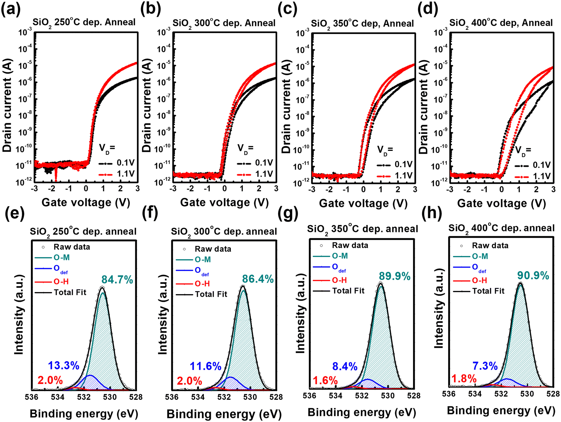
Fig. 3(a)–(d) shows the I–V transfer curves of IGZO-channel TG FETs at different SiO2 GI deposition temperatures. The post-annealing process was not conducted after FET fabrication. Except for the SiO2 deposition temperature, the process conditions of the FET, such as the IGZO cation ratio, deposition temperature, and electrode material, were the same. The transfer curve of the FET exhibited a counterclockwise hysteresis independent of the SiO2 deposition temperature. The mobile ionic charge and electrical dipoles of GI possibly result in the counterclockwise hysteresis of the FET.40 Here, the mobile ionic charge of the GI has the potential to cause counterclockwise hysteresis because SiO2 has a low dielectric constant of approximately four and is not a ferroelectric material. In general, hydrogen, potassium, lithium, and sodium ions act as mobile ionic charges.41 Hydrogen impurities in SiO2 are a potential reason for the counterclockwise hysteresis of the FET because potassium and sodium were not detected by XPS analysis (Fig. S1, ESI†). The trend of the hysteresis values on SiO2 deposition temperature is similar to the trend of the hydrogen-related binding area percentage, as shown in Table 1 and Fig. 2(f)–(i). Hydrogen impurities in SiO2 and optimization of the electrical properties are discussed later. Increasing the deposition temperature of the SiO2 GI of the FET lowered the on-current, and Vth showed a positive shift. These results indicated that the electrical properties of the IGZO channel were affected by the SiO2 deposition process. Fig. 3(e)–(h) presents the XPS O 1s peak deconvolution results for the bonding state of oxygen in IGZO. XPS analysis was conducted on the SiO2 (10 nm)/IGZO (50 nm) stacked structure and the SiO2 layer was Ar ion-etched before the analysis. The XPS depth profile was conducted to define the IGZO bulk region to deconvolution, as shown in Fig. S2 (ESI†). The XPS O 1s peak of IGZO was deconvoluted into three subpeaks: metal and oxygen binding (M–O), oxygen deficiency (Odef), and hydrogen-related binding (O–H), which corresponded to 529.8 ± 0.1, 531.1 ± 0.1, and 532.1 ± 0.1 eV, respectively.22 The percentage of Odef and O–H peak area decreased with the SiO2 deposition temperature increase because of the ozone exposure and post-annealing effect during the SiO2 GI deposition.42,43 This indicated that the conductivity of IGZO was lowered by the reduction of oxygen vacancy and hydrogen-related bonding, which generated electron carriers during ozone exposure and the reaction during SiO2 deposition.22,44 Consequently, although the film quality of the SiO2 dielectric was improved by increasing the deposition temperature, the conductivity of IGZO was degraded by ozone exposure during deposition.
 | ||
| Fig. 3 (a)–(d) I–V transfer curves of FETs and (e)–(h) XPS O 1s peak deconvolution results of IGZO in SiO2/IGZO stacked films according to the SiO2 deposition temperature; (a), (e) 250, (b), (f) 300, (c) and (g) 350, and (d) and (h) 400 °C, respectively. The post-annealing process was not conducted. | ||
| SiO2 dep. Temp. | 250 °C | 300 °C | 350 °C | 400 °C | ||||
|---|---|---|---|---|---|---|---|---|
| Post process | As | Anneal. | As | Anneal. | As | Anneal. | As | Anneal. |
| V th [V] | N/A | 0.4 ± 0.1 | −2.0 ± 0.1 | 0.2 ± 0.1 | −1.0 ± 0.1 | 0.1 ± 0.1 | 0.5 ± 0.1 | 0.2 ± 0.1 |
| μ FE [cm2 V−1 s−1] | N/A | 21.1 ± 1.2 | 69.3 ± 9.1 | 19.0 ± 1.1 | 53.5 ± 0.5 | 18.4 ± 0.2 | 19.9 ± 1.9 | 17.4 ± 0.5 |
| Hysteresis [V] | N/A | 0.07 ± 0.01 | 1.77 ± 0.02 | 0.22 ± 0.03 | 0.82 ± 0.02 | 0.35 ± 0.01 | 0.56 ± 0.02 | 0.60 ± 0.08 |
| Mobile ionic charge density [cm−2] | 8.0 × 10¹¹ | 5.5 × 10¹⁰ | 6.6 × 10¹¹ | 1.4 × 10¹¹ | 4.2 × 10¹¹ | 2.1 × 10¹¹ | 4.1 × 10¹¹ | 4.1 × 10¹¹ |
| S.S. [V dec−1] | N/A | 0.10 ± 0.01 | 0.13 ± 0.05 | 0.14 ± 0.01 | 0.09 ± 0.04 | 0.13 ± 0.01 | 0.11 ± 0.02 | 0.14 ± 0.02 |
To improve the hysteresis voltage of the FET, a post-annealing process was conducted at 500 °C in an Ar atmosphere for 1 h to reduce the hydrogen content in SiO2. The electrical parameters extracted from the I–V transfer curves of the as-deposited and post-annealed FET are summarized in Table 1. The output curves are presented in Fig. S3 (ESI†). Fig. 4(a)–(d) show that the counterclockwise hysteresis was improved in the post-annealed FETs, regardless of the SiO2 deposition temperature. However, more than 1 V of hysteresis was still exhibited except for the 250 °C SiO2 deposited FET. The μFE decreased with the SiO2 deposition temperature because of the decreasing IGZO conductivity; 21.1, 19.0, 18.4, and 17.4 cm2 V−1 s−1 for deposited at 250, 300, 350, and 400 °C, respectively. Consequently, whereas the SiO2 film properties improved with the deposition temperature, the electrical properties of the post-annealed FET were superior at lower temperatures. As shown in Fig. S4 (ESI†), the optimal annealing temperature was 500 °C. The post-annealing process significantly decreases the on-current. The 200 °C deposited SiO2 GI FETs exhibit inferior electrical properties compared to 250 °C deposited SiO2 GI FETs because the 200 °C is not within the ALD process window (Fig. S5, ESI†). XPS analysis was conducted on the SiO2/IGZO structure after post-annealing to observe the oxygen-binding state of IGZO, and the results are shown in Fig. 4(e)–(h). The Odef binding percentage decreased with increasing SiO2 deposition temperature, a trend similar to that observed for the as-deposited films. However, the Odef binding percentages were lower than those of the as-deposited films, regardless of the SiO2 deposition temperature. Because the post-annealing atmosphere was argon, the increased M–O binding of IGZO could have originated from the insertion of oxygen-related molecules during SiO2 reduction or reaction with ozone.
 | ||
| Fig. 4 (a)–(d) I–V transfer curves of FET and (e)–(h) XPS O 1s peak deconvoluting results of IGZO in SiO2/IGZO stacked films according to the SiO2 deposition temperature; (a) and (e) 250, (b) and (f) 300, (c) and (g) 350, and (d) and (h) 400 °C, respectively. Post-annealing was conducted at 500 °C in an Ar atmosphere for 1 h. | ||
To confirm the origin of the counterclockwise hysteresis of the SiO2 GI FET, the ionic mobile charge density (QM) was extracted from the charge-pumping BTS method by measuring the difference of flat-band voltage after the bias stress (the temperature and stress were 200 °C and ±1 MV cm−1, respectively). The C–V measurements were conducted in the MOS region of TG FET, as shown in Fig. 5(a). The calculated dielectric constant results measured at 1000 Hz of frequency and used to extract the electrical properties of FETs are presented in Fig. S6 (ESI†). Compared to the results shown in Fig. S6 (ESI†), it was confirmed that a flat-band voltage difference occurred owing to the ionic mobile charge. Interestingly, the trend of QM corresponded to the hysteresis trend of the FETs (Fig. 5(b)–(i)); QM decreased with the SiO2 deposition temperature in the as-deposited films, whereas the opposite trend was observed for the post-annealed films. Furthermore, the QM values decreased significantly after post-annealing, independent of the SiO2 deposition temperature. This result indicates that a counterclockwise hysteresis occurs owing to the mobile ionic charge originating from the hydrogen content of SiO2.45
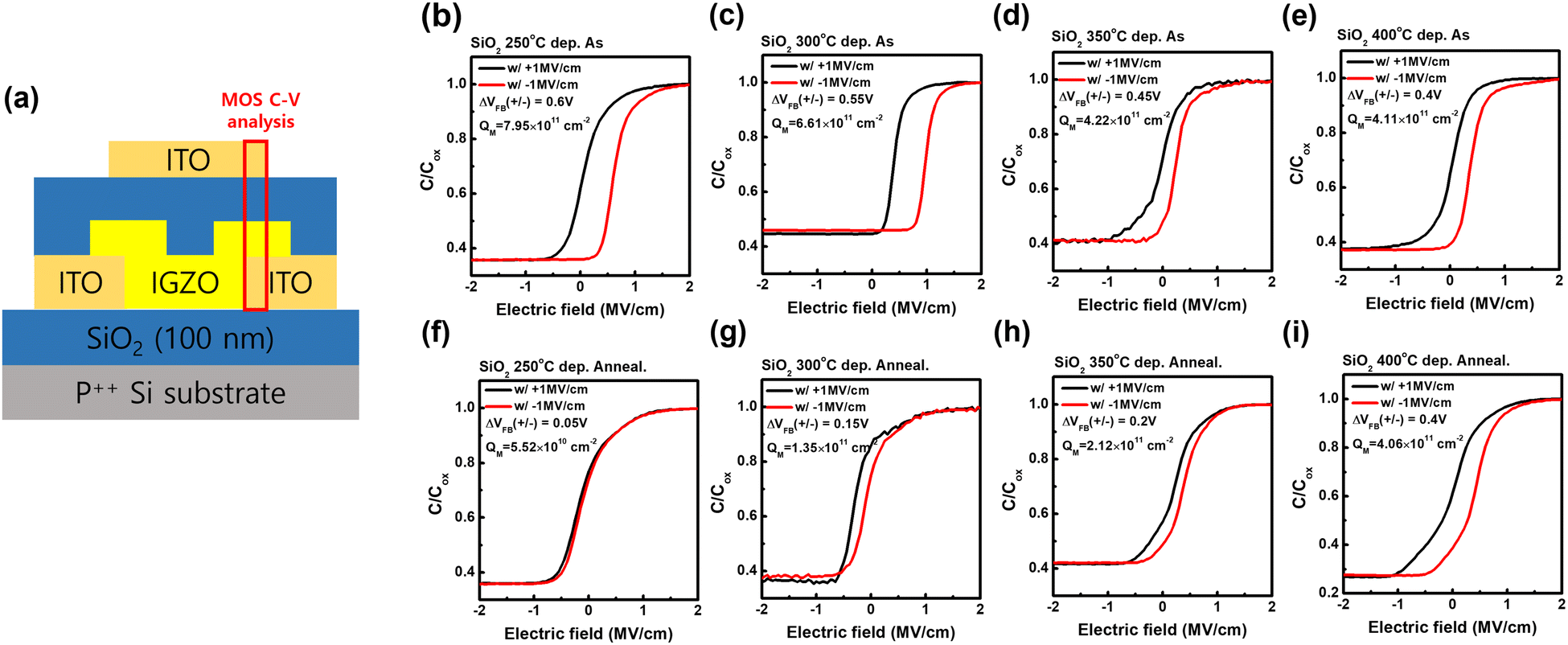 | ||
| Fig. 5 (a) Schematics of the TG FET and MOS C–V analysis using the charge-pumping BTS technique. The C–V analysis results and extracted ionic mobile charge density for as-deposited and post-annealed FETs according to a SiO2 deposition temperature of (b) and (f) 250 °C, (c) and (g) 300 °C, (d) and (h) 350 °C, and (e) and (i) 400 °C. | ||
A D-SIMS depth profile analysis was conducted to compare the hydrogen intensities of SiO2 and IGZO in terms of the GI deposition temperature. As shown in Fig. 6, the hydrogen content of IGZO as-deposited increased with a decrease in the SiO2 deposition temperature. Because the IGZO fabrication conditions, such as deposition temperature and ozone density, were equal, the different hydrogen contents of IGZO would originate from the diffusion by SiO2. The hydrogen content coincided with the trend of the mobile ionic charge density of SiO2 and the counterclockwise hysteresis of the FET after the post-annealing process. This confirmed that the hydrogen content of SiO2 acted as a mobile ionic charge and increased the counterclockwise hysteresis. Interestingly, more hydrogen content of SiO2 and IGZO diffuses out at lower SiO2 deposition temperatures during the post-annealing process; the hydrogen reduction percentages of SiO2 and IGZO were 48.7% and 63.9%, 21.4% and 58.8%, 4.0% and 51.1%, and 4.4% 21.1% at a SiO2 deposition temperature of 250, 300, 350, 400 °C, respectively. Because hydrogen from SiO2 and IGZO diffuses out through the SiO2 films, the hydrogen reduction percentage differences possibly originate from the quality of the SiO2 film, such as its density. Fig. S8 (ESI†) shows that the reduction of SiO2 did not occur during the post-annealing process. The hydrogen contents of SiO2 are presented in Fig. S9 (ESI†). Furthermore, as shown in Fig. S10 (ESI†), the hydrogen atomic density trend according to the deposition temperature and post-annealing process of SiO2 films was double-checked by RBS and ERD analysis.
 | ||
| Fig. 6 D-SIMS depth profiles of hydrogen intensity for (a) as-deposited and (b) annealed SiO2/IGZO films according to the SiO2 deposition temperature. Hydrogen intensity results of the (c) SiO2 and (d) IGZO regions. | ||
Because the mobile ionic charge and hydrogen content of the GI degraded the reliability properties of the FET, positive- and negative-bias stress (PBS and NBS, respectively) reliability tests were conducted at 0.1 V of VDS. The transfer curves and Vth shift values are presented in Fig. 7 and Fig. S11 (ESI†). The Vth shifts of PBS (1 MV cm−1) and NBS (−1 MV cm−1) at 3 h were −0.19 and +0.25 V, −0.45 and +0.45 V, −0.50 and +0.49 V, and −0.56 and +0.49 V at SiO2 deposition temperatures of 250, 300, 350, and 400 °C, respectively. An abnormal negative Vth shift during PBS originated from the electron carrier generation by hydrogen diffusion to the channel.46 And an abnormal positive Vth shift during NBS originated from the hydrogen mobile ionic charge migration to the gate electrode.47
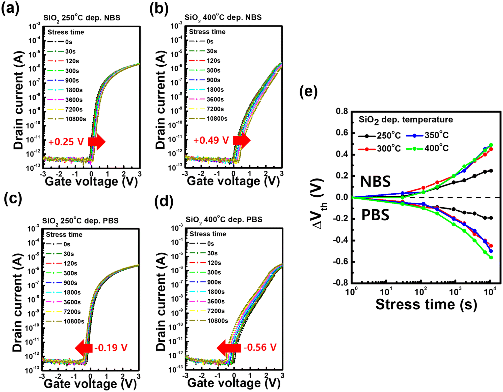 | ||
| Fig. 7 Transfer characteristics and Vth shift values during the P(N)BS reliability tests for the (a) and (c) 250 and (b) and (d) 400 °C SiO2 deposited FETs. (e) Vth shift values according to the SiO2 deposition temperature and stress time. | ||
The Vth shift increased with the SiO2 deposition temperature because the hydrogen content of the post-annealed SiO2 increased with the deposition temperature. Consequently, considering not only the GI film quality but also the hydrogen content trend during the post-annealing process is necessary for optimizing the properties of the transistor. It is because the hydrogen content of GI can affect the electrical and reliability properties by acting on the ionic mobile charge trap density and film quality such as density affects the hydrogen diffusion.
3. Conclusions
In this study, we optimized the electrical and reliability properties of an IGZO-channel TG FET by controlling the hydrogen content of SiO2. The film quality of the as-deposited SiO2, including the breakdown voltage, dielectric constant, density, binding state, and hydrogen impurity content, increased with increasing deposition temperature. However, the conductivity of IGZO decreased with increasing SiO2 deposition temperature because of the reaction with ozone and lowering of the oxygen vacancy state, which generates carriers during deposition. Because the hydrogen content of SiO2 acts as a mobile ionic charge trap, which degrades the FET properties, a post-annealing process is required. The percentage of diffused-out hydrogen decreased with the SiO2 deposition temperature. The 250 °C deposited SiO2 GI FET exhibits a high μFE of 21.1 cm2 V−1 s−1, Vth of 0.4 V, and S. S. of 100 mV dec−1 with a superior stability of −0.19 and +0.25 V shift during PBS and NBS at 1 MV cm−1 stress conditions for 3 h by lowering the hydrogen content. These results show that considering the effect of each layer, such as channel and GI, is more significant than considering the properties of a single layer itself.4. Experimental
4.1. Thin-film fabrication and characterization
The IGZO active layer and SiO2 gate electric films were deposited via ALD using ozone with a 200 g m−3 density as the reactant. The deposition temperature of the IGZO was 250 °C. (3-Dimethylaminopropyl)dimethyl indium (DADI) heated to 45 °C, trimethylgallium (TMGa), and diethylzinc (DEZ) were used as the indium, gallium, and zinc precursors, respectively. The super-cycle of the IGZO cations was 1:1:1. The SiO2 deposition temperature was varied from 200 to 400 °C in 50 °C intervals, and BTBAS was used as a silicon source. The purge gas was argon and the working pressure was maintained at 1.2 mTorr using a throttle valve. The thickness and refractive index (RI) of the films were measured using a spectroscopic ellipsometer (Elli-SE(UV)-FM8, Ellipso Technology). X-ray photoelectron spectroscopy (XPS, K-Alpha+, Thermo Fisher Scientific) was used to investigate the presence of carbon, nitrogen, potassium, and sodium impurities and the ratio of the metal and oxygen bonding states within the film. The film density was evaluated by X-ray reflectance (XRR; Smartlab, RIGAKU). To investigate the variations in the O and H signals in the SiO2/IGZO stacked films as a function of the SiO2 deposition temperature and post-annealing process, dynamic secondary ion mass spectrometry (D-SIMS; IMS-7F_Auto, CAMECA, UK) was conducted using a cesium ion source at 6keV. The hydrogen concentration of SiO2 films was calculated using the reference sample (Evans Analytical Group). The hydrogen atomic density was calculated using Rutherford back scattering spectroscopy (RBS) and elastic recoil detection (ERD) analyses (NEC, National Electrostatics Corporation).
4.2. Device fabrication
A staggered TG FET was fabricated on a 100-nm thick thermally grown SiO2 substrate. The 100-nm thick indium tin oxide (ITO) layer was deposited as the source and drain electrodes using radio-frequency magnetron sputtering. The IGZO active layers were deposited at a thickness of 10 nm. Next, a 10-nm thick SiO2 gate dielectric was deposited at various temperatures ranging from 250 to 400 °C. Finally, a 100-nm thick ITO layer was deposited as the gate electrode. Photolithography patterning and wet etching were used to define the electrodes, channels, and dielectric layers. After FET fabrication, the post-annealing process was conducted at 400, 500, and 600 °C in an Ar atmosphere for 1 h. The channel length and width of the FET were 40 and 20 μm, respectively. The overlapped area of ITO electrodes was designated as 400 μm2 regardless of the misalignment of a photolithography process.4.3. Device evaluation and characterization
All devices were evaluated using a Keithley 4200 semiconductor analyzer. The gate-source voltage (Vgs) was swept from −3 to 3 V (positive bias) and 3 to −3 V (negative bias) at the drain–source voltage (VDS) = 0.1 and 1.1 V to measure the transfer characteristics. The output characteristics were measured under the following conditions: Vgs was increased from 0 to 5 V in 1 V intervals and VDS was swept from 0 to 5 V. The μFE of the FET was extracted from the linear transfer characteristics, given by μFE = Lgm(max)/(WCoxVds) at a VDS of 0.1 and 1.1 V. Here, gm(max) is the maximum transconductance, W is the channel width of the transistor, and Cox is the oxide capacitance of the GI. The threshold voltage (Vth) was calculated using the linear extrapolation method.48 Hysteresis is the difference in Vth between the positive- and negative-bias gate voltage sweeps. The subthreshold swing (S. S.) is the lowest value calculated using the following equation: S. S. = dVgs/dlog(Id), where Vgs is the gate voltage and Id is the drain current density. The electrical property values of TG FETs were extracted at 0.1 V of VDS. Capacitance–voltage (C–V) characteristics were measured using an LCR meter (HP 4284A). The mobile ionic charge density was extracted from the C–V results using a charge-pumping technique with bias-temperature stress (BTS) in the MOS structure. The BTS condition was ±1 MV cm−1 at 200 °C for 2 min.
Author contributions
Su-Hwan Choi: methodology, investigation, writing – original Draft. Dong-Gyu Kim: methodology, investigation, writing – original draft. Jae-Hyeok Kwag: methodology, investigation. Ki-Cheol Song: methodology, investigation. Yeonhee Lee: methodology, investigation. Chang-Kyun Park: funding acquisition. Jin-Seong Park: conceptualization, supervision, writing – review & editing. S.-H. Choi and D.-G. Kim contributed equally to this study.Data availability
The authors declare that all data supporting the results reported in this study are available within the paper and the ESI.† Additional data used for the study are available from the corresponding author upon reasonable request.Conflicts of interest
The authors declare that they have no known competing financial interests or personal relationships that could have appeared to influence the work reported in this paper.Acknowledgements
This research was supported by the Technology Innovation Program (20017382 and 20023023), funded by the Ministry of Trade, Industry & Energy (MOTIE, Korea). This research was also supported by a National Research Foundation of Korea (NRF) grant funded by the Korean government (MSIT) (No. RS-2023-00260527). The JUSUNG Engineering Corp. also supports this research.References
- T. Kamiya, N. Kenji and H. Hideo, Sci. Technol. Adv. Mater., 2010, 11.4, 044305 CrossRef PubMed.
- J. Sheng, T. Hong, D. Kang, Y. Yi, J. H. Lim and J. S. Park, ACS Appl. Mater. Interfaces, 2019, 11.13, 12683–12692 CrossRef PubMed.
- J. Sheng, T. H. Hong, H. M. Lee, K. R. Kim, M. Sasase, J. Kim, H. Hosono and J. S. Park, ACS Appl. Mater. Interfaces, 2019, 11.43, 40300–40309 CrossRef PubMed.
- A. Sen, H. Park, P. Pujar, A. Bala, H. Cho, N. Liu, S. Gandla and S. Kim, ACS Nano, 2022, 16.6, 9267–9277 CrossRef.
- S. Knobelspies, B. Bierer, A. Daus, A. Takabayashi, G. A. Salvatore, G. Cantarella, A. O. Perez, J. Wöllenstein, S. Palzer and G. Tröster, Sensors, 2018, 18.2, 358 CrossRef.
- K. Nomura, J. Inf. Disp., 2021, 22.4, 211–229 CrossRef.
- S. Jeong, S. Jang, H. Han, H. Kim and C. Choi, J. Alloys Compd., 2021, 888, 161440 CrossRef CAS.
- X. Duan, K. Huang, J. Feng, J. Niu, H. Qin, S. Yin, G. Jiao, D. Leonelli, X. Zhao, Z. Wang, W. Jing, Z. Wang, Y. Wu, J. Xu, Q. Chen, X. Chuai, C. Lu, W. Wang, G. Yang, D. Geng, L. Li and M. Liu, IEEE Trans. Electron Devices, 2022, 69.4, 2196–2202 Search PubMed.
- X. Yu, T. J. Marks and A. Facchetti, Nat. Mater., 2016, 15.4, 383–396 CrossRef.
- S. H. Choi, S. H. Ryu, D. G. Kim, J. H. Kwag, C. Yeon, J. Jung, Y. S. Park and J. S. Park, Nano Lett., 2024, 24.4, 1324–1331 CrossRef.
- H. J. Joo, M. G. Shin, H. S. Jung, H. S. Cha, D. Nam and H. I. Kwon, Materials, 2019, 12.23, 3815 CrossRef.
- Y. Su, M. Shi, J. Tang, Y. Li, Y. Du, R. An, J. Li, Y. Li, J. Yao, R. Hu, Y. He, Y. Xi, Q. Li, S. Qiu, Q. Zhang, L. Pan, B. Gao, H. Qian and H. Wu, IEEE Trans. Electron Devices, 2024, 71.5, 3336–3342 Search PubMed.
- K. Huang, X. Duan, J. Feng, Y. Sun, C. Lu, C. Chen, G. Jiao, X. Lin, J. Shao, S. Yin, J. Sheng, Z. Wang, W. Zhang, X. Chuai, J. Niu, W. Wang, Y. Wu, W. Jing, Z. Wang, J. Xu, G. Yang, D. Geng, L. Li and M. Liu, IEEE Symp. VLSI Circuits Dig. Tech. Pap., 2022, 296–297 Search PubMed.
- D. G. Kim, S. H. Choi, W. B. Lee, G. M. Jeong, J. Koh, S. Lee, B. Kuh and J. S. Park, Small Struct., 2024, 5.2, 2300375 CrossRef.
- J. Stankiewicz, X. Torrelles, J. L. García-Muñoz and J. Blasco, J. Alloys Compd., 2017, 694, 1280–1286 CrossRef CAS.
- J. H. Noh, S. Y. Ryu, S. J. Jo, C. S. Kim, S. W. Sohn, P. D. Rack, D. J. Kim and H. K. Baik, IEEE Electron Device Lett., 2010, 31.6, 567–569 Search PubMed.
- H. Park, Y. Nam, J. Jin and B. S. Bae, RSC Adv., 2015, 5, 102362–102366 RSC.
- M. Girtan and G. Folcher, Surf. Coat. Technol., 2003, 172, 242–250 CrossRef CAS.
- M. H. Cho, C. H. Choi, H. J. Seul, H. C. Cho and J. K. Jeong, ACS Appl. Mater. Interfaces, 2021, 13.14, 16628–16640 CrossRef.
- D. G. Kim, W. B. Lee, S. Lee, J. Koh, B. Kuh and J. S. Park, ACS Appl. Mater. Interfaces, 2023, 15.30, 36550–36563 CrossRef PubMed.
- S. M. George, Chem. Rev., 2010, 110.1, 111–131 CrossRef.
- S. H. Choi, T. H. Hong, S. H. Ryu and J. S. Park, Ceram. Int., 2022, 48.19, 27807–27814 CrossRef.
- Y. S. Kim, H. J. Oh, J. Kim, J. H. Lim and J. S. Park, Small methods, 2023, 7.10, 2300549 CrossRef.
- J. M. Lee, I. T. Cho, J. H. Lee and H. I. Kwon, Appl. Phys. Lett., 2008, 93, 093504 CrossRef.
- H. Y. Noh, W. G. Lee, G. R. Haripriya, J. H. Cha, J. S. Kim, W. S. Yun, M. J. Lee and H. J. Lee, Sci. Rep., 2022, 12, 19816 CrossRef CAS PubMed.
- Y. Nam, H. O. Kim, S. H. Cho and S. H. K. Park, RSC Adv., 2018, 8, 5622–5628 RSC.
- S. R. Thomas, P. Pattanasattayavong and T. D. Anthopoulos, Chem. Soc. Rev., 2013, 42, 6910–6923 RSC.
- S. G. Jeong, H. J. Jeong, W. H. Choi, K. R. Kim and J. S. Park, IEEE Trans. Electron Devices, 2020, 67.10, 4250–4255 Search PubMed.
- A. Teramoto, H. Umeda, K. Aamawari, K. Kabayashi, K. Shiga, J. Komori, Y. Ohno and A. Shigetomi, Microelectron. Reliab., 2001, 41.1, 47–52 CrossRef.
- G. Fang, L. Xu, J. Ma and A. Li, Chem. Mater., 2016, 28, 1247–1255 CrossRef CAS.
- M. Putkonen, M. Bosund, O. M. E. Ylivaara, R. L. Puurunen, L. Kilpi, H. Ronkainen, S. Sintonen, S. Ali, H. Lipsanen, X. Liu, E. Haimi, S. P. Hannula, T. Sajavaara, I. Buchanan, E. Karwacki and M. Vähä-Nissi, Thin Solid Films, 2014, 558, 93–98 CrossRef CAS.
- T. Nam, H. Lee, T. Choi, S. Seo, C. M. Yoon, Y. Choi, H. Jeong, H. K. Lingam, V. R. Chitturi, A. Korolec, J. H. Ahn and H. Kim, Appl. Surf. Sci., 2019, 485, 381–390 CrossRef CAS.
- B. Han, Q. Zhang, J. Wu, B. Han, E. J. Karwacki, A. Derecskei, M. Xiao, X. Lei, M. L. O’Neill and H. Cheng, J. Phys. Chem. C, 2012, 116.1, 947–952 CrossRef.
- L. F. Peña, C. E. Nanayakkara, A. Mallikarjunan, H. Chandra, M. Xiao, X. Lei, R. M. Pearlstein, A. Derecskei-Kovacs and Y. J. Chabal, J. Phys. Chem. C, 2016, 120.20, 10927–10935 CrossRef.
- K. Ide, Y. Kikuchi, K. Nomura, T. Kamiya and H. Hosono, Thin Solid Films, 2012, 520.10, 3787–3790 CrossRef.
- K. Umeda, T. Miyasako, A. Sugiyama, A. Tanaka, M. Suzuki, E. Tokumitsu and T. Shimoda, J. Appl. Phys., 2013, 113.18, 184509 CrossRef.
- C. Oh, T. Kim, M. W. Ju, M. Y. Kim, S. H. Park, G. H. Lee, H. Kim, S. Kim and B. S. Kim, Materials, 2023, 16.18, 6161 CrossRef.
- R. Alfonsetti, L. Lozzi, M. Passacantando, P. Picozzi and S. Santucci, Appl. Surf. Sci., 1993, 70, 222–225 CrossRef.
- R. Huang, M. Tang, W. Kan, H. Xu, K. Wu, Z. Wang and H. Li, J. Phys. D:Appl. Phys., 2023, 57.1, 015102 Search PubMed.
- Z. Ye, Y. Yuan, H. Xu, Y. Liu, J. Luo and M. Wong, IEEE Trans. Electron Devices, 2017, 64.2, 438–446 Search PubMed.
- T. Prodromakis, P. Georgiou, K. Michelakis and C. Toumazou, IEEE Int. Symp. Circuits Syst., 2009, 2165–2168 Search PubMed.
- K. J. Gan, P. T. Liu, D. B. Ruan, Y. C. Chiu and S. M. Sze, Vacuum, 2020, 180, 109630 CrossRef CAS.
- W. P. Zhang, S. Chen, S. B. Qian and S. J. Ding, Semicond. Sci. Technol., 2014, 30.1, 015003 Search PubMed.
- M. D. H. Chowdhury, M. Mativenga, J. G. Um, R. K. Mruthyunjaya, G. N. Heiler, T. J. Tredwell and J. Jang, IEEE Trans. Electron Devices, 2015, 62.3, 869–874 Search PubMed.
- A. Chanthaphan, T. Hosoi, S. Mitani, Y. Nakano, T. Nakamura, T. Shimura and H. Watanabe, Appl. Phys. Lett., 2012, 100, 252103 CrossRef.
- Y. S. Kim, T. Hwang, H. J. Oh, J. S. Park and J. S. Park, Adv. Mater. Interfaces, 2024, 11.15, 2301097 CrossRef.
- C. Lo, Z. L. Feng, W. L. Huang, C. W. Liu, T. L. Chen and C. H. Chou, IEEE J. Electron Devices Soc., 2016, 4.5, 353–357 Search PubMed.
- Y. Swami and S. Rai, Circ. Syst., 2016, 7.13, 4248–4279 CrossRef.
Footnotes |
| † Electronic supplementary information (ESI) available. See DOI: https://doi.org/10.1039/d4tc04277h |
| ‡ S.-H. Choi and D.-G. Kim contributed equally to this work. |
| This journal is © The Royal Society of Chemistry 2025 |