
Nonvolatile electrical control of the electronic and valleytronic properties by ferroelectricity in the VSi2P4/Al2S3 van der Waals heterostructure†
Shoubao
Zhang
 a,
Na
Jiao
a,
Hongyan
Lu
a,
Mengmeng
Zheng
a,
Ping
Zhang
ab and
Meiyan
Ni
*a
a,
Na
Jiao
a,
Hongyan
Lu
a,
Mengmeng
Zheng
a,
Ping
Zhang
ab and
Meiyan
Ni
*a
aSchool of Physics and Physical Engineering, Qufu Normal University, Qufu 273165, China. E-mail: nimy@qfnu.edu.cn
bInstitute of Applied Physics and Computational Mathematics, Beijing 100088, China
First published on 25th October 2024
Abstract
In this paper, based on first-principles theory, we investigated the properties of the multiferroic VSi2P4/Al2S3 van der Waals (vdW) heterostructure (HS), in which VSi2P4 and Al2S3 are ferromagnetic (FM) and ferroelectric (FE) materials, respectively. Our results show that the properties of the VSi2P4 layer can be effectively manipulated by reversing the ferroelectric polarized state of the Al2S3 layer (P↑ and P↓). Specifically, for P↓ Al2S3, VSi2P4 preserves the semiconductor nature and the intrinsic valley polarization in the conduction band. However, for P↑ Al2S3, the VSi2P4 sublayer is changed to a half-metal, and the valley polarization in the conduction band is submerged in trivial bands. Our findings provide an effective way for nonvolatile electrical control of the electronics and valleytronics of 2D ferromagnetic materials.
1. Introduction
Over the past few decades, the two-dimensional (2D) material family has grown at a remarkable speed. Hundreds of materials have been fabricated experimentally or have been proposed to be stable theoretically.1–4 These 2D materials present many unique properties and are intended to be applied in many fields.5–9 However, 2D ferromagnetic (FM) materials have not been fabricated experimentally for a long time, which has limited their application in spintronic devices and ultrahigh-density magnetic storage. Great breakthroughs have been made by Zhang's group and Xu's group, who experimentally observed intrinsically ferromagnetic behavior in bilayer Cr2Ge2Te610 and monolayer CrI3,11 respectively. Since then, an increasing number of 2D van der Waals (vdW) magnetic materials have been fabricated experimentally, such as Fe3GeTe2,12 MnPS3,13 VSe2,14 MnBi2Te4,15 Fe3GaTe2,16 and so on. These materials exhibit different magnetic properties and transport properties and provide excellent platforms for fundamental physics research.17–25Nevertheless, for the practical application of 2D magnetic materials, many issues must be addressed, such as increasing the critical temperature (TC) to room temperature and effectively modulating the electronic and magnetic properties. In addition to the discovery of new 2D magnetic materials, various strategies have been recognized to be useful for manipulating the properties of 2D magnets. One of the most representative example is the building of a multiferroic vdW heterostructure constructed from 2D FM and ferroelectric (FE) materials, which have strong interfacial magnetoelectric effects. Many 2D multiferroic heterostructures have been investigated theoretically and compared with isolated FM materials, and it was inferred that their transport properties,26–31 magnetic order,32 magnetic anisotropy,33–35 Curie temperature,36 and valleytronic properties37–41 can be effectively manipulated by FE materials. 2D FE materials possess two stable polarized states (P↑ and P↓), whose polarized directions are opposite. For example, the electric polarization direction of In2Se3 is out-of-plane. By applying a short-term external field, the bistable polarized states can be switched from one to another.42,43 When the FE and FM materials form heterostructures, FE materials provide a spontaneous polarization electric field, which can control the electronic properties of FM materials. Notably, this polarized electric field is nonvolatile even if the external field is removed, and thus, the electrical control of the FM materials is also theoretically nonvolatile. Therefore, the use of multiferroic HSs is an effective strategy for realizing nonvolatile magnetoelectric nanodevices, and it is highly important to select suitable FM and FE materials to construct multiferroic HSs and explore their excellent physical properties.
Recently, single-layer MSi2N4 (M = Mo, W) was successfully synthesized experimentally.44 Many ternary compounds with similar structures have been proposed to be stable and exhibit various properties such as intrinsic magnetism, spin–valley properties, and nontrivial band topology.45–48 In this work, we chose VSi2P4 as the FM material and Al2S3 as the FE material to construct vdW multiferroic VSi2P4/Al2S3 heterostructures. The VSi2P4 monolayer is a ferromagnetic semiconductor and presents exotic spontaneous valley polarization which facilitates the appearance of the anomalous valley Hall effect.49,50 Al2S3 is predicted to be a ferroelectric material with an out-of-plane polarization direction, which belongs to the well-known ferroelectric family of In2Se3. On the basis of first-principles calculations, we systematically investigated the electronic properties of the multiferroic VSi2P4/Al2S3 vdW heterostructures. Our results show that by reversing the electric polarization direction of Al2S3, VSi2P4 can be switched from a semiconductor to a half-metal and obtain an on-to-off transition of the valley nature. The underlying mechanism was unveiled via the band alignment and charge redistribution analysis. These results provide a promising scheme for nonvolatile control of the electronic and valleytronic properties of 2D FM materials and pave the way for the application of the VSi2P4/Al2S3 HS in electronic devices.
2. Computational details
In this work, structural relaxation and electronic property calculations were performed using density functional theory (DFT)51 and the Vienna ab initio simulation package (VASP). The electron–ion interaction was described using the projector-augmented-wave (PAW) method.52 The Perdew–Burke–Ernzerhof (PBE) functional under the generalized gradient approximation (GGA) was chosen for the exchange–correlation function.53,54 A plane-wave cutoff of 500 eV was employed. The Brillouin zone was sampled with a k-point of 12 × 12 × 1 for structural relaxation and a k-point of 18× 18 × 1 for property calculations.55 The correlation effects for the V-3d electrons were treated by the DFT+U method with Ueff = 3 eV.56 The band structure was also calculated by using the Heyd–Scuseria–Ernzerhof hybrid functional method (HSE06).57 The structure was optimized with convergence criteria for energy and force of 10−6 eV per atom and 0.01 eV Å−1, respectively. To minimize the periodic mirror interaction, a vacuum space of 20 Å along the z direction was used to avoid interactions between adjacent layers. The vdW interaction between VSi2P4 and Al2S3 was described using the DFT-D3 correction method of Grimme et al.58,59 To rule out spurious dipole–dipole interactions between periodic images, the dipole correction was considered. The phonon spectrum was calculated through the density functional perturbation theory (DFPT) approach via the PHONOPY code.603. Results and discussion
3.1. Structural and electronic properties of isolated VSi2P4 and Al2S3 monolayers
We first investigated the structure and properties of the pristine VSi2P4 and Al2S3 monolayers. The lattice parameter and atom positions of these two monolayers are fully optimized. The crystal structure of the VSi2P4 monolayer is shown in Fig. 1(a), which exhibits a hexagonal lattice with a space group of P![[6 with combining macron]](https://www.rsc.org/images/entities/char_0036_0304.gif) m2. It is composed of septuple atomic layers stacked in the sequence of P–Si–P–V–P–Si–P along the z axis. Importantly, the inversion symmetry is broken in this structure. The lattice parameter of the VSi2P4 monolayer is optimized to 3.512 Å at the PBE+U level. The stability is investigated by performing phonon spectrum calculations. The spectrum plotted in Fig. S1 (in the ESI†) shows no soft phonon mode throughout the Brillouin zone (BZ), indicating the dynamical stability of the structure. To determine the magnetic ground state, we calculated the total energy of the VSi2P4 monolayer with different magnetic configurations based on a 2 × 2 × 1 supercell, including nonmagnetic (NM), FM, zig-zag-antiferromagnetic (AFM-z), and stripe-antiferromagnetic (AFM-s) configurations (Fig. S2 in ESI†). The energy differences among the four magnetic states are shown in Table S1 (ESI†). It is found that the magnetic ground state of the VSi2P4 monolayer is an FM material with a magnetic moment of 1μB per unit cell. The distribution of the magnetic moment on every atom is presented in Table S2 (ESI†), which shows that the magnetic moment of the V atom is 1.1μB and there is weak antiferromagnetic moment distribution around the neighboring P atoms.
m2. It is composed of septuple atomic layers stacked in the sequence of P–Si–P–V–P–Si–P along the z axis. Importantly, the inversion symmetry is broken in this structure. The lattice parameter of the VSi2P4 monolayer is optimized to 3.512 Å at the PBE+U level. The stability is investigated by performing phonon spectrum calculations. The spectrum plotted in Fig. S1 (in the ESI†) shows no soft phonon mode throughout the Brillouin zone (BZ), indicating the dynamical stability of the structure. To determine the magnetic ground state, we calculated the total energy of the VSi2P4 monolayer with different magnetic configurations based on a 2 × 2 × 1 supercell, including nonmagnetic (NM), FM, zig-zag-antiferromagnetic (AFM-z), and stripe-antiferromagnetic (AFM-s) configurations (Fig. S2 in ESI†). The energy differences among the four magnetic states are shown in Table S1 (ESI†). It is found that the magnetic ground state of the VSi2P4 monolayer is an FM material with a magnetic moment of 1μB per unit cell. The distribution of the magnetic moment on every atom is presented in Table S2 (ESI†), which shows that the magnetic moment of the V atom is 1.1μB and there is weak antiferromagnetic moment distribution around the neighboring P atoms.
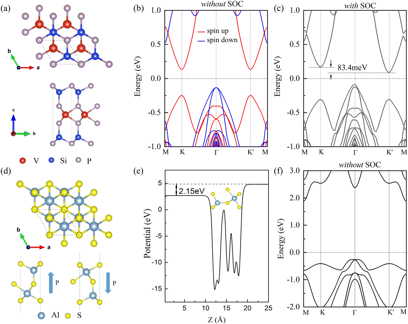 | ||
| Fig. 1 (a) Top and side views of the VSi2P4 monolayer. Band structures of the VSi2P4 monolayer (b) without and (c) with the SOC effect. (d) Top and side views of the Al2S3 FE material in the P↑ and P↓ polarized states. (e) Plane-averaged electrostatic potential along the z direction and (f) the band structure of the Al2S3 monolayer. The dashed boxes in (a) and (d) represent the unit cells of VSi2P4 and Al2S3. The Fermi level is set to zero. | ||
Fig. 1(b) presents the band structure of the VSi2P4 monolayer in the absence of spin–orbital coupling (SOC). It is shown that the spin-up and spin-down bands split significantly. The VSi2P4 monolayer exhibits a semiconducting character with an indirect band gap of 0.26 eV at the PBE+U level, which is in good agreement with previous work.49 Its valence band maximum (VBM) is located at the Γ point and the conduction band minimum (CBM) is located at the K and K′ points, forming a pair of degenerate valleys in the conduction band. As the inversion symmetry for VSi2P4 is broken, the degenerated valleys are inequivalent. In Fig. 1(c), after considering the SOC, the K valley shifts above the K′ valley in the conduction band in energy, indicating spontaneous valley polarization in the conduction band. The valley polarization is 83.4 meV. For the valence band, there is also a pair of degenerate valleys at the K and K′ points, and only a 2 meV valley polarization appears after the SOC effect is considered. As mentioned above, the VSi2P4 monolayer is a 2D FM valleytronic semiconductor.
As shown in Fig. 1(d), the 2D Al2S3 monolayer is a quintuple layer structure with the S–Al–S–Al–S sequence. The calculated lattice parameter of Al2S3 is 3.591 Å, which agrees well with a previous study.39 It exhibits spontaneous electric polarization in the out-of-plane direction. The two FE polarization states are denoted as P↑ and P↓, corresponding to the central S layer aligning with the lower and upper Al layers. As shown in Fig. 1(e), the plane-averaged electrostatic potential of Al2S3 is calculated, with the potential energy difference between the two sides being 2.15 eV. To confirm the dynamical stability of Al2S3, the phonon spectrum was calculated with no soft phonon mode throughout the BZ (Fig. S3, ESI†). We further calculated the band structure of Al2S3 without SOC. As presented in Fig. 1(f), the pristine Al2S3 monolayer is an indirect semiconductor with a band gap of 2.08 eV.
To verify the correctness of the energy band structure of VSi2P4 and Al2S3 monolayers, the HSE06 method is used. By comparing Fig. 1 and Fig. S4 (ESI†), for both VSi2P4 and Al2S3 monolayers, the band structures obtained by the PBE+U method and HSE06 method are similar, and only the band gap and valley polarization values are different. For the VSi2P4 monolayer, it is an indirect energy band semiconductor with the band gap increased from 0.26 eV (PBE+U) to 0.70 eV (HSE06). After considering SOC interaction, a valley polarization of about 47.9 meV is preserved in the conduction band between the K and K′ points, which is little smaller than that calculated using the PBE+U method. For the Al2S3 monolayer, it is still an indirect semiconductor with the band gap increased from 2.08 eV (PBE+U) to 2.94 eV (HSE06).
3.2. Structural properties of the multiferroic VSi2P4/Al2S3 HS
All the heterostructures were relaxed with the lattice parameters fixed and the atom positions were fully optimized. As the magnetic properties are sensitive to the lattice parameters of the structure, the unit cell of the 2D FM VSi2P4 material is adopted as the unit cell of the VSi2P4/Al2S3 HS, with a lattice parameter of 3.512 Å. The lattice parameter mismatch between VSi2P4 and Al2S3 is 2.2%, which can be easily achieved in the experimental fabrication of such a HS. As shown in Fig. S5 (ESI†), six different stacking configurations of the VSi2P4/Al2S3 HS are considered for two polarized states of Al2S3, named UP-1…UP-6 and DW-1…DW-6. UP and DW indicate the directions of the electric polarization of Al2S3. To confirm the most stable stacking configuration, the total energy, binding energy and interlayer distance of different stacking configurations were calculated (Table 1). The binding energy (Eb) between VSi2P4 and Al2S3 is defined as Eb = (EVSi2P4 + EAl2S3 − EHS)/S. Here, EVSi2P4, EAl2S3 and EHS are the energies of the VSi2P4 monolayer, Al2S3 monolayer and VSi2P4/Al2S3 HS, respectively. S is the interfacial area. The positive binding energies imply that all stacking configurations are energetically stable. Table 1 shows that, for both electric polarization directions, UP-1 and DW-1 are most stable with the lowest total energy, strongest binding energy and shortest interlayer distances. The side views of UP-1 and DW-1 are shown in Fig. 2(a) and (d) with electric polarization in the up and down directions. In these two structures, the relative positions of the atoms in adjacent layers are the same: the P atom in the bottom layer of VSi2P4 is aligned above the hollow site of Al2S3 and the Si atom lies above the top site of the Al atom in the first layer of Al2S3. The magnetic ground states of the UP-1 and DW-1 HSs are investigated by calculating the total energies of four different magnetic configurations (FM, NM, AFM-s, and AFM-z) on the basis of a 2 × 2 × 1 supercell. The relative energies of the four magnetic configurations are shown in Table S3 (ESI†). The FM state is preserved as the ground state of the heterostructures.| Configuration | Energy (eV) | E b (meV Å−1) | Distance (Å) | Configuration | Energy (eV) | E b (meV Å−1) | Distance (Å) |
|---|---|---|---|---|---|---|---|
| UP-1 | −67.6010 | 176.01 | 3.280 | DW-1 | −67.6041 | 176.26 | 3.254 |
| UP-2 | −67.5987 | 175.82 | 3.281 | DW-2 | −67.5976 | 175.74 | 3.259 |
| UP-3 | −67.5442 | 171.45 | 3.785 | DW-3 | −67.5454 | 171.50 | 3.785 |
| UP-4 | −67.5966 | 175.65 | 3.280 | DW-4 | −67.6020 | 176.06 | 3.254 |
| UP-5 | −67.6003 | 175.95 | 3.281 | DW-5 | −67.6013 | 175.95 | 3.259 |
| UP-6 | −67.5445 | 171.48 | 3.785 | DW-6 | −67.5450 | 171.47 | 3.771 |
 | ||
| Fig. 2 Structures of the VSi2P4/Al2S3 HS with polarization directions (a) up and (d) down. Band structures of the VSi2P4/Al2S3 HS in the P↑ Al2S3 state (b) without and (c) with SOC. Band structures of the HS in the P↓ Al2S3 state (e) without and (f) with SOC. | ||
Although the total energies of UP-1 and DW-1 HS are the lowest, the energy differences of some heterostructures are very small. The specific energy difference is shown in Table S4 (ESI†). Under room-temperature conditions, the thermal energy is around 26 meV which is much larger than the energy difference of some configurations. For example, the energy difference between UP-1 and UP-5 is only 0.7 meV. Therefore, besides UP/DW-1 heterostructures, the heterostructures with other stacking sequence are possible at room temperature, such as UP/DW-2 and UP/DW-4 heterostructures.
3.3. Electronic and valleytronic properties of the multiferroic VSi2P4/Al2S3 HS
Next, we investigated the electronic properties of the VSi2P4/Al2S3 HS. The band structures of the six different stacking configurations for both electric polarization directions are presented in Fig. S7 and S8 (ESI†). It is found that the band structures with the same electric polarization direction are extremely similar, and there is only a very small difference when we zoomed in the band structures of UP-1 to UP-6 heterostructures around the Fermi level, as shown in Fig. S9 (ESI†). Therefore, the stacking configuration of the heterostructures does not affect the main electronic properties of heterostructures, and in the following part only the band structures of the UP-1 and DW-1 configurations are discussed in detail. In Fig. 2(b) and (e), the band structures without considering SOC are shown. For the UP-1 configuration (Fig. 2(b) and Fig. S9(a), ESI†), the HS is a metal with the Fermi level crossing the conduction band. The orbital-resolved band structure of UP-1 shown in Fig. S10(a) (ESI†) reveals that this conduction band is attributed to the spin-up channels of VSi2P4. Therefore, the VSi2P4 sublayer presents half-metallic properties with 100% spin polarization. For the Al2S3 sublayer, it maintains semiconducting properties. For the DW-1 configuration, the band structure shown in Fig. 2(e) indicates that the HS is a semiconductor with an indirect band gap of 0.25 eV. The VBM and CBM are contributed by spin-down and spin-up channels of VSi2P4, and the band alignment type of the DW-1 HS is type-I (Fig. S10(b), ESI†). To check the results, the HSE06 functional is used to calculate the band structures of UP-1 HS and DW-1 HS, as shown in Fig. S11 (ESI†). For the UP-1 heterostructure, it is a metal with the Fermi level crossing both the VBM and the CBM, and there is an obvious overlap between the VBM and the CBM. For the DW-1 heterostructure, it is an indirect semiconductor with a band gap of 0.75 eV, which is larger than the result obtained by the PBE+U method. Therefore, both the PBE+U and HSE06 methods present a similar result. That is, there is a transition from a metal to a semiconductor by reversing the direction of the electric polarized direction.The band structures of UP-1 and DW-1 considering SOC are shown in Fig. 2(c) and (f). For the UP-1 configuration (Fig. 2(c)), the Fermi level crosses both the conducting band and the valence band. The projected band structure shown in Fig. 3(a) presents that around the Fermi level, the conducting band around the K′ point is contributed by VSi2P4 and the valence band is contributed by the Al2S3 layer. This indicates that both VSi2P4 and Al2S3 sublayers are metallic. For the DW-1 case (Fig. 2(f)), the VSi2P4/Al2S3 HS preserves the semiconducting properties with an indirect band gap of 0.19 eV. As shown in Fig. 3(b), both the VBM and CBM are contributed by VSi2P4, whereas the bands from Al2S3 are located far from the Fermi level. Therefore, when SOC is considered, a transition from a metal to a semiconductor upon switching of the ferroelectric states of Al2S3 is also presented.
 | ||
| Fig. 3 Projected band structures of the VSi2P4/Al2S3 HS in (a) the P↑ and (b) P↓ polarized states with the SOC effect. Here, the red and blue symbols denote the contributions from the Al2S3 layer and VSi2P4 layer, respectively. | ||
Aside from the transition from a metal to a semiconductor, Fig. 2(c) and (f) also show that the energy degeneracy between the K and K′ valleys is lifted in both the conduction band and the valence band, which originates the breaking of the time-reversal symmetry. Specifically, for the UP-1 configuration, Fig. 2(c) and 3(a) show that there is an overlap between the CBM at the K′ site and the VBM at the Γ site occupied by Al2S3. This overlap results in the valley at the K′ site being submerged in the trivial bands from Al2S3 and restricts any potential application of these valleys. For the DW-1 configuration, Fig. 2(f) and 3(b) show that the intrinsic valley polarization in the conduction band is preserved, with a valley spin splitting of 78.0 meV, which is similar to that of the isolated VSi2P4 monolayer. This value is much larger than that of some experimentally demonstrated magnetic proximity systems61 and can resist the annihilation of valley polarization near room temperature. Unlike the case of the conduction band, the valley polarization in the valence band is almost zero for both electric polarization states, and they are submerged in the trivial bands, resulting in no potential application. Therefore, according to the discussion above, under FE switching, the VSi2P4/Al2S3 HS experiences a transition from a metal to a semiconductor and a transition of valley polarization from turn-off to turn-on.
To understand the mechanism of the different electronic properties of VSi2P4/Al2S3 in different electric polarization states, we investigated the band alignment between isolated VSi2P4 and Al2S3 monolayers. When VSi2P4 monolayers contact Al2S3 in different polarized states, different band alignment configurations are presented in Fig. 4(a). For the Al2S3 case in the P↑ state, the VBM of Al2S3 is located above the CBM of VSi2P4, which prompts electron transfer from Al2S3 to VSi2P4 and induces the metallicity of heterostructure. In contrast, for the Al2S3 case in the P↓ state, the VBM of Al2S3 is located below the CBM of VSi2P4, which inhibits the electron transfer between two adjacent monolayers. Therefore, in this polarization state, the semiconductor properties and valley polarization are preserved. The different charge transfer characteristics of these heterostructures can also be seen from the charge density difference (Δρ), as illustrated in Fig. 4(b) and (c). Besides, the charge depletion and accumulation spatial distribution are also calculated, as shown in Fig. S12 (ESI†). Both kinds of charge density differences indicate that the interfacial charge transfer between Al2S3 and VSi2P4 is much stronger for the upward polarization state than the downward polarization state, which induces an upshift of the Fermi level in the UP-1 configuration.
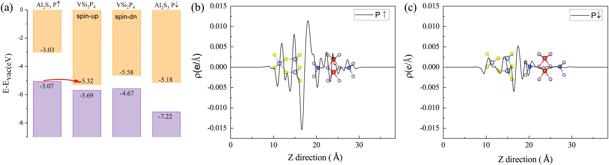 | ||
| Fig. 4 (a) Band alignment of the VSi2P4 monolayer (spin-up and spin-down) and the Al2S3 monolayer (P↑ and P↓) with respect to the vacuum level. The plane-averaged charge density difference along the z direction in the (b) P↑ and (c) P↓ polarized states. The negative value represents a charge depletion region and the positive value represents a charge accumulation region. | ||
The band structures of the VSi2P4/Al2S3 heterostructures with different stacking configurations considering SOC are shown in Fig. S13 and S14 (ESI†). For upward electric polarization, as shown in Fig. S13 (ESI†), all the HSs are metal, and for downward electric polarization, as shown in Fig. S14 (ESI†), all the HSs are semiconductors. Therefore, regardless of the stacking sequence, the transport properties can be changed from a metal to a semiconductor by switching the direction of electric polarization. Additionally, we found that there is a reverse of valley polarization among different heterostructures. For example, in Fig. S13 (ESI†), for DW-1, DW-2, and DW-3, the CBM at the K point is higher than that at the K′ point, and for DW-4, DW-5, and DW-6, the CBM at the K point is lower than that at the K′ point. The reversal of the valley polarization comes from the difference in the stacking sequences. As shown in Fig. S6 (ESI†), the UP(DW)-4, UP(DW)-5, and UP(DW)-6 configurations are obtained from the UP(DW)-1, UP(DW)-2, and UP(DW)-3 configurations by rotating the VSi2P4 sublayer in 60° counterclockwise with the P atom (in red circle) as the center and keeping the Al2S3 sublayer fixed. With such an operation, the locations of the atoms are in two different sublattices in VSi2P4 switch. For example, for the Si atom (in red circles) and the P atom (in black circles) in Fig. S6(a) and (f) (ESI†), their locations in sublattices are exchanged, and the exchange of inequivalent sublattice locations induces the reversal of valley polarization at the K point and K′ point.
Magnetic anisotropy energy (MAE) is a crucial factor for magnetic materials; therefore, further calculation was performed to investigate the changes of MAE. MAE is defined as the energy difference between out-of-plane and in-plane magnetization: MAE = Ez − Ex. Our results show that the MAE of monolayer VSi2P4 is −28 μeV, suggesting that its easy axis is along the out-of-plane direction. We further calculated the MAE of the heterostructures. The results show that the MAE of the UP-1 configuration is −327 μeV and that of the DW-1 configuration is −26 μeV, suggesting that its easy axis is not changed after constructing the heterostructures with Al2S3. However, the MAE of the UP-1 configuration increases significantly, which is conducive to the FM state stability of the VSi2P4/Al2S3 heterostructure.
4. Conclusions
In summary, we proposed a multiferroic VSi2P4/Al2S3 heterostructure formed from an FM VSi2P4 monolayer and an FE Al2S3 monolayer. When VSi2P4 monolayers contact P↓ Al2S3, semiconducting properties remain, but they turn into metals when P↓ Al2S3 is electronically switched to P↑ Al2S3. Moreover, the valley polarization of the VSi2P4 monolayer also involves reversible switching from turn-on to turn-off with the electric polarization of Al2S3. Therefore, this work provides a possible scheme for reversible and nonvolatile control of the electronics and valleytronics of 2D ferrovalley and FM material VSi2P4.Data availability
The data supporting this article have been included as part of the ESI.†Conflicts of interest
There are no conflicts to declare.Acknowledgements
This work is supported by the National Natural Science Foundation of China (Grant No. 12074213, 11574108, and 12104253), the Major Basic Program of the Natural Science Foundation of Shandong Province (Grant No. ZR2021ZD01), the Natural Science Foundation of Shandong Provincial (Grant No. ZR2023MA082) and the Project of Introduction and Cultivation for Young Innovative Talents in Colleges and Universities of Shandong Province.References
- K. F. Mak, C. Lee, J. Hone, J. Shan and T. F. Heinz, Phys. Rev. Lett., 2010, 105, 136805 CrossRef PubMed.
- K. Xu, Z. Wang, X. Du, M. Safdar, C. Jiang and J. He, Nanotechnology, 2013, 24, 465705 CrossRef.
- M. Naguib, V. N. Mochalin, M. W. Barsoum and Y. Gogotsi, Adv. Mater., 2014, 26, 992 CrossRef CAS PubMed.
- Y. L. Hong, Z. B. Liu, L. Wang, T. Y. Zhou, W. Ma, C. Xu, S. Feng, L. Chen, M. L. Chen, D. M. Sun, X. Q. Chen, H. M. Cheng and W. C. Ren, Science, 2021, 12, 2361 Search PubMed.
- C. C. Liu, W. Feng and Y. Yao, Phys. Rev. Lett., 2011, 107, 076802 CrossRef.
- H. J. Zhang, C. X. Liu, X. L. Qi, X. Dai, Z. Fang and S. C. Zhang, Nat. Phys., 2009, 5, 438 Search PubMed.
- H. Y. Lu, Y. Yang, L. Hao, W. S. Wang, L. Geng, M. M. Zheng, Y. Li, N. Jiao, P. Zhang and C. S. Ting, Phys. Rev. B, 2020, 101, 214514 CrossRef CAS.
- P. C. Xiao, L. Yang, H. Y. Lu, N. Hao and P. Zhang, Phys. Rev. B, 2024, 109, 054506 CrossRef CAS.
- Y. J. Ji, M. Y. Yang, H. L. Dong, T. J. Hou, L. Wang and Y. Y. Li, Nanoscale, 2017, 9, 8608 RSC.
- C. Gong, L. Li, Z. Li, H. Ji, A. Stern, Y. Xia, T. Cao, W. Bao, C. Wang, Y. Wang, Z. Q. Qiu, R. J. Cava, S. G. Louie, J. Xia and X. Zhang, Nature, 2017, 546, 265 CrossRef CAS.
- B. Huang, G. Clark, E. Navarro-Moratalla, D. R. Klein, R. Cheng, K. L. Seyley, D. Zhong, E. Schmidgall, M. A. McGuire, D. H. Cobden, W. Yao, D. Xiao, P. Jarillo-Herrero and X. D. Xu, Nature, 2017, 546, 270 CrossRef CAS.
- Z. Y. Fei, B. Huang, P. Malinowski, W. B. Wang, T. C. Song, J. Sanchez, W. Yao, D. Xiao, X. Y. Zhu, A. F. May, W. D. Wu, D. H. Cobden, J. H. Chu and X. D. Xu, Nat. Mater., 2018, 17, 778 CrossRef CAS.
- G. Long, H. Henck, M. Gibertini, D. Dumcenco, Z. Wang, T. Taniguchi, K. Watanabe, E. Giannini and A. F. Morpurgo, Nano Lett., 2020, 20, 2452 CrossRef CAS PubMed.
- R. Chua, J. Yang, X. Y. He, X. J. Yu, W. Yu, F. Bussolotti, P. K. J. Wong, K. P. Loh, M. B. H. Breese, K. E. J. Goh, Y. L. Huang and A. T. Wee, Adv. Mater., 2020, 32, 2000693 CrossRef CAS.
- Y. J. Deng, Y. J. Yu, M. Z. Shi, Z. X. Guo, Z. H. Xu, J. Wang, X. H. Chen and Y. B. Zhang, Science, 2020, 367, 895 CrossRef CAS.
- G. J. Zhang, F. Guo, H. Wu, X. K. Wen, L. Yang, W. Jin, W. F. Zhang and H. X. Chang, Nat. Commun., 2022, 13, 5067 CrossRef CAS PubMed.
- X. Jiang, Q. X. Liu, J. P. Xing, N. S. Liu, Y. Guo, Z. F. Liu and J. J. Zhao, Appl. Phys. Rev., 2021, 8, 031305 CAS.
- S. N. Kajale, J. Hanna, K. Jang and D. Sarkar, Nano Res., 2024, 17, 743 CrossRef.
- Y. J. Ahn, X. Y. Guo, S. H. Son, Z. L. Sun and L. Y. Zhao, Prog. Quantum Electron., 2024, 93, 100498 CrossRef.
- Q. H. Wang, X. L. Yang, F. W. Zhang and P. Zhang, J. Phys. Chem. C, 2024, 128, 6852 CrossRef CAS.
- W. Y. Tong, S. J. Gong, X. G. Wan and C. G. Duan, Nat. Commun., 2016, 7, 13612 CrossRef CAS PubMed.
- J. Chen, X. N. Wang, Y. P. An and S. J. Gong, J. Phys.: Condens. Matter, 2024, 38, 083001 CrossRef.
- Z. Wang, I. Gutiérrez-Lezama, N. Ubrig, M. Kroner, M. Gibertini, T. Taniguchi, K. Watanabe, A. Imamoglu, E. Giannini and A. F. Morpurgo, Nat. Commun., 2018, 9, 2516 CrossRef PubMed.
- D. R. Klein, D. MacNeill, J. L. Lado, D. Soriano, E. Navarro-Moratalla, K. Watanabe, T. Taniguchi, S. Manni, P. Canfield, J. Fernández-Rossier and P. Jarillo-Herrero, Nano Lett., 2019, 19, 5133 CrossRef PubMed.
- W. Xun, C. Wu, H. Sun, W. Zhang, Y.-Z. Wu and P. Li, Nano Lett., 2024, 24, 3541 CrossRef CAS PubMed.
- C. Gong, E. M. Kim, Y. Wang, G. Lee and X. Zhang, Nat. Commun., 2019, 10, 2657 CrossRef.
- X. Y. Liu, C. H. Shen, X. P. Li, T. X. Wang, M. J. He, L. Li, Y. Wang, J. B. Li and C. X. Xia, Nanoscale, 2022, 14, 5454 RSC.
- L. Z. Li and B. Z. Zhou, J. Mater. Chem., 2020, 8, 4534 Search PubMed.
- Y. H. Zhao, J. J. Zhang, S. J. Yuan and Z. F. Chen, Adv. Funct. Mater., 2019, 29, 1901420 CrossRef.
- P. Jiang, L. Li Kang, H. Hao, X. Hong Zheng, Z. Zeng and S. Sanvito, Phys. Rev. B, 2020, 102, 245417 CrossRef CAS.
- X. Zhang, B. Liu, J. S. Huang, X. W. Cao, Y. Z. Zhang and Z. X. Guo, Phys. Rev. B, 2024, 109, 205105 CrossRef CAS.
- W. Sun, W. X. Wang, D. Chen, Z. X. Cheng and Y. X. Wang, Nanoscale, 2019, 11, 9931 RSC.
- L. Yin and D. S. Parker, Phys. Rev. B, 2020, 102, 054441 CrossRef CAS.
- Y. P. Wang, X. G. Xu, X. Zhao, W. X. Ji, Q. Cao, S. S. Li and Y. L. Li, npj Comput. Mater., 2022, 8, 218 CrossRef.
- A. Ilyas, S. L. Xiang, M. G. Chen, M. Y. Khan, H. Bai, P. M. He, Y. H. Lu and R. R. Deng, Nanoscale, 2021, 13, 1069 RSC.
- F. Xue, Z. Wang, Y. S. Hou, L. Gu and R. Q. Wu, Phys. Rev. B, 2020, 101, 184426 CrossRef CAS.
- C. G. Lei, X. L. Xu, T. Zhang, B. B. Huang, Y. Dai and Y. D. Ma, J. Phys. Chem. C, 2021, 125, 2802 CrossRef CAS.
- W. H. Du, Z. L. He, Y. Dai, B. B. Huang and Y. D. Ma, npj 2D Mater. Appl., 2022, 6, 11 CrossRef CAS.
- C. G. Lei, X. R. Li, Y. D. Ma and Z. Qian, Phys. Rev. B, 2023, 106, 155431 CrossRef.
- Y. Chen, G. Z. Wang, J. T. Guo, M. X. Li, H. K. Yuan and H. Chen, ACS Appl. Nano Mater., 2024, 7, 4302 CrossRef CAS.
- P. Li, C. Wu, C. Peng, M. Yang and W. Xun, Phys. Rev. B, 2023, 108, 195424 CrossRef CAS.
- C. Cui, W. Hu, X. Yan, C. Addiego, W. Gao, Y. Wang, Z. Wang, L. Li, Y. Cheng, P. Li, X. Zhang, H. N. Alshareef, T. Wu, W. Zhu, X. Pan and L. Li, Nano Lett., 2018, 18, 1253 CrossRef CAS.
- F. Xue, W. Hu, K. C. Lee, L. S. Lu, J. Zhang, H. L. Tang, A. Han, W. T. Hsu, S. Tu, W. H. Chang, C. H. Lien, Z. He, J. H. Zhang, L. J. Li and X. Zhang, Adv. Funct. Mater., 2018, 28, 1803738 CrossRef.
- Y. L. Hong, Z. B. Liu, L. Wang, T. Y. Zhou, W. Ma, C. Xu, S. Feng, L. Chen, M. L. Chen, D. M. Sun, X. Q. Chen, H. M. Cheng and W. C. Ren, Science, 2020, 369, 670 CrossRef CAS PubMed.
- L. Wang, Y. Shi, M. Liu, A. Zhang, Y. L. Hong, R. Li, Q. Gao, M. Chen, W. Ren, H. M. Cheng and Y. Li, Nat. Commun., 2021, 12, 2361 CrossRef CAS.
- I. M. Verzola, R. A. Villaos, Z.-Q. Huang, C.-H. Hsu, Y. Okada, H. Lin and F.-C. Chuang, J. Phys. Chem. C, 2024, 128, 6829 CrossRef CAS.
- M. R. K. Akanda and R. K. Lake, Appl. Phys. Lett., 2021, 119, 052402 CrossRef CAS.
- P. Li, X. Yang, Q.-S. Jiang, Y.-Z. Wu and W. Xun, Phys. Rev. Mater., 2023, 7, 064002 CrossRef CAS.
- X. Y. Feng, X. L. Xu, Z. L. He, R. Peng, Y. Dai, B. B. Huang and Y. D. Ma, Phys. Rev B, 2021, 104, 075421 CrossRef CAS.
- S. Li, Q. Q. Wang, C. M. Zhang, P. Guo and S. A. Yang, Phys. Rev. B, 2021, 104, 085149 CrossRef CAS.
- W. Kohn, A. D. Becke and R. G. Parr, J. Phys. Chem., 1996, 100, 12974 CrossRef CAS.
- P. E. Blöchl, Phys. Rev. B: Condens. Matter Mater. Phys., 1994, 50, 17953 CrossRef PubMed.
- J. P. Perdew and Y. Wang, Phys. Rev. B: Condens. Matter Mater. Phys., 1992, 46, 12947 CrossRef.
- J. P. Perdew and Y. Wang, J. Comput. Chem., 2006, 27, 1787 CrossRef.
- H. J. Monkhorst and J. D. Pack, Phys. Rev. B: Condens. Matter Mater. Phys., 1976, 13, 5188 CrossRef.
- S. L. Dudarev, G. A. Botton, S. Y. Savrasov, C. J. Humphreys and A. P. Sutton, Phys. Rev. B: Condens. Matter Mater. Phys., 1998, 57, 1505 CrossRef CAS.
- J. Heyd, G. E. Scuseria and M. Ernzerhof, J. Chem. Phys., 2003, 118, 8207 CrossRef CAS.
- S. Grimme, J. Antony, S. Ehrlich and H. Krieg, J. Chem. Phys., 2010, 132, 154104 CrossRef PubMed.
- S. Grimme, S. Ehrlich and L. Goerigk, J. Comput. Chem., 2011, 32, 1456 CrossRef CAS PubMed.
- A. Togo and I. Tanaka, Scr. Mater., 2015, 108, 1 CrossRef CAS.
- K. L. Seyler, D. Zhong, B. Huang, X. Linpeng, N. P. Wilson, T. Taniguchi, K. Watanabe, W. Yao, D. Xiao, M. A. McGuire, K. M. C. Fu and X. D. Xu, Nano Lett., 2015, 18, 3823 CrossRef PubMed.
Footnote |
| † Electronic supplementary information (ESI) available. See DOI: https://doi.org/10.1039/d4tc03592e |
| This journal is © The Royal Society of Chemistry 2025 |