
 Open Access Article
 This Open Access Article is licensed under a
 Creative Commons Attribution 3.0 Unported Licence
ZnGa2Te4 thin-film absorbers for photoelectrochemical CO2 reduction†
Shaham
Quadir
 *a,
Yungchieh
Lai
b,
Melissa K.
Gish
a,
John S.
Mangum
a,
Wayne
Zhao
cd,
Ruo Xi
Yang
d,
Mona
Abdelgaid
d,
Christopher P.
Muzzillo
a,
Kristin A.
Persson
cd,
Joel A.
Haber
b,
Sage R.
Bauers
a and
Andriy
Zakutayev
*a
*a,
Yungchieh
Lai
b,
Melissa K.
Gish
a,
John S.
Mangum
a,
Wayne
Zhao
cd,
Ruo Xi
Yang
d,
Mona
Abdelgaid
d,
Christopher P.
Muzzillo
a,
Kristin A.
Persson
cd,
Joel A.
Haber
b,
Sage R.
Bauers
a and
Andriy
Zakutayev
*a
aNational Renewable Energy Laboratory, Golden, Colorado 80401, USA. E-mail: shaham.quadir@nrel.gov; andriy.zakutayev@nrel.gov
bCalifornia Institute of Technology, Pasadena, California 91125, USA
cUniversity of California, Berkeley, California 94720, USA
dLawrence Berkeley National Laboratory, Berkeley, California 94720, USA
First published on 21st July 2025
Abstract
Photoelectrochemical (PEC) carbon dioxide reduction reaction (CO2RR) has been considered as a promising route to convert and store solar energy into chemical fuels. It is crucial to find suitable photoelectrode materials that are photo-catalytically active and exhibit excellent photochemical stability. One of the promising contenders is ZnTe with the ∼2.26 eV band gap and prolonged stability under CO2RR PEC conditions. Herein, a new telluride based thin-film ZnGa2Te4 photocathode with lower band gap and stronger visible light absorption compared to ZnTe is synthesized and characterized using a combinatorial sputtering technique. A two-step annealing method with excess Te supply is implemented to synthesize nearly stoichiometric ZnGa2Te4 absorber material with a zincblende-derived tetragonal crystal structure confirmed by synchrotron X-ray and electron diffraction. Theoretical calculations show that ZnGa2Te4 has suitable direct bandgap (∼1.86 eV) and high absorption coefficient ∼105 cm−1, in agreement with experimentally prepared films. Transient absorption spectroscopy reveals the biexponential decay dynamics, with time constants, τ1 ∼ 0.04, and τ2 ∼ 0.65 μs in microsecond time scales and provides the optical transition pathways for this semiconductor thin film. PEC measurements show that the ZnGa2Te4 photocurrent densities are comparable to the widely investigated ZnTe photocathodes or even surpass it under simulated sunlight condition. ZnGa2Te4 samples demonstrate promising photoelectrochemical stability, maintaining consistent performance under illumination. The inclusion of diaryliodonium additive substantially increases its CO2RR selectivity to ∼60%. These findings open a new avenue for the synthesis of telluride-based thin-film photocathodes for further exploration and will motivate future research to integrate this potential photocathode material into PEC devices.
Introduction
Photoelectrochemical (PEC) carbon dioxide reduction reaction (PEC CO2RR) technology is one of the emerging pathways to advanced energy solutions.1,2 PEC CO2RR based-on semiconductor photoelectrodes can convert solar energy into chemical fuels. This process mimics natural photosynthesis and it provides a solution to fulfill our world's increasing energy demand. To achieve PEC CO2 reduction, it is important to find a photoabsorber with specific optical properties including appropriate band edge positions, robustness in harsh aqueous environments, and high activity for CO2RR.3,4 A range of different semiconductor materials such as Si, oxides (Cu2O, Fe2O3, BiVO4, CeO2), metal organic frameworks (MOFs) and nitrides, i.e. ZnTiN2 have been studied as potential photoelectrodes for PEC CO2RR.5–10Recently chalcogenide-based semiconductor materials have received attention due to their interesting photovoltaic characteristics. Cu(In,Ga)(S,Se)2,11 CZTS12 and CuGa3Se5![[thin space (1/6-em)]](https://www.rsc.org/images/entities/char_2009.gif) 13 chalcopyrite photocathodes have shown promising results for PEC applications. The zinc blende phase of ZnTe has been tested and exhibits photocatalytic activity toward both H2 evolution (HER) and CO2RR.14 A recent study showed that tailoring the surface composition of ZnTe photocathodes could result in an improved interfacial charge transfer, effectively modifying its CO2RR activity and selectivity before adding any electrocatalysts.15 The optoelectronic properties of sputtered ZnTe could be improved by chloride treatments and the measured faradaic efficiency (FE) can be increased using organic additives.16 However, the ∼2.26 eV band gap of ZnTe is wider than ideal for the operation as a photocathode, calling for new material searches.
13 chalcopyrite photocathodes have shown promising results for PEC applications. The zinc blende phase of ZnTe has been tested and exhibits photocatalytic activity toward both H2 evolution (HER) and CO2RR.14 A recent study showed that tailoring the surface composition of ZnTe photocathodes could result in an improved interfacial charge transfer, effectively modifying its CO2RR activity and selectivity before adding any electrocatalysts.15 The optoelectronic properties of sputtered ZnTe could be improved by chloride treatments and the measured faradaic efficiency (FE) can be increased using organic additives.16 However, the ∼2.26 eV band gap of ZnTe is wider than ideal for the operation as a photocathode, calling for new material searches.
There have been several computational screening studies for materials that may be suitable as cathodes for CO2RR. A recent study identified 17 telluride photocathodes among 52 candidates with excellent aqueous stability under operational conditions.17 Another theoretical screening study emphasizes the promising CO2RR activity of tellurium-containing semiconductors and suggests Te-based photo absorbers possess more thermodynamically favorable conditions to convert CO2 to chemical fuels.18 Based on the optical properties and considering excitonic effects, 4 telluride photocathode materials that are suitable for visible-light photocatalysis have been short-listed, including GaTe, Cd(GaTe2)2, LiInTe2, and Zn(GaTe2)2.19 Most of these tellurides have been synthesized using the Bridgman technique, CVT and also solid state reaction for powder and bulk characterization.20–22
Herein, we develop a synthesis route of tellurium based thin-film photocathodes ZnGa2Te4 using combinatorial sputtering techniques. We demonstrate that adjusting the cation (Zn, Ga) to anion (Te) ratio, facilitate a phase transition from cubic (F![[4 with combining macron]](https://www.rsc.org/images/entities/char_0034_0304.gif) 3m) to tetragonal (I) crystal symmetry during post-deposition annealing. Notably, excess of Te in as-deposited film is required to form stable tetragonal ZnGa2Te4 structure after annealing. DFT calculation show that ZnGa2Te4 is direct bandgap semiconductor (bandgap 1.86 eV) with high absorption coefficient (105 cm−1) that are consistent with optical measurements and suitable for effective sunlight absorption compared to ZnTe (2.26 eV band gap). Transient absorption (TA) spectroscopy at time scales from 100 fs through 10 μs shows the photoexcited carrier kinetics of the ZnGa2Te4 photocathode with a promising carrier lifetime for the photoelectrode applications. Photoelectrochemical (PEC) analyses are conducted, revealing that ZnGa2Te4 exhibits performance comparable to other chalcogenide-based semiconductors such as ZnTe benchmark photoelectrode. Finally, the ZnGa2Te4 films show a promising photo-current density with efficient fuel production and inclusion of diaryliodonium additive suppresses HER and significantly improves CO2RR to become the major reaction. Notably, ZnGa2Te4 maintained stable photocurrent and consistent product formation during PEC stability test.
3m) to tetragonal (I) crystal symmetry during post-deposition annealing. Notably, excess of Te in as-deposited film is required to form stable tetragonal ZnGa2Te4 structure after annealing. DFT calculation show that ZnGa2Te4 is direct bandgap semiconductor (bandgap 1.86 eV) with high absorption coefficient (105 cm−1) that are consistent with optical measurements and suitable for effective sunlight absorption compared to ZnTe (2.26 eV band gap). Transient absorption (TA) spectroscopy at time scales from 100 fs through 10 μs shows the photoexcited carrier kinetics of the ZnGa2Te4 photocathode with a promising carrier lifetime for the photoelectrode applications. Photoelectrochemical (PEC) analyses are conducted, revealing that ZnGa2Te4 exhibits performance comparable to other chalcogenide-based semiconductors such as ZnTe benchmark photoelectrode. Finally, the ZnGa2Te4 films show a promising photo-current density with efficient fuel production and inclusion of diaryliodonium additive suppresses HER and significantly improves CO2RR to become the major reaction. Notably, ZnGa2Te4 maintained stable photocurrent and consistent product formation during PEC stability test.
Results and discussion
(ZnTe)x(Ga2Te3)1−x materials family
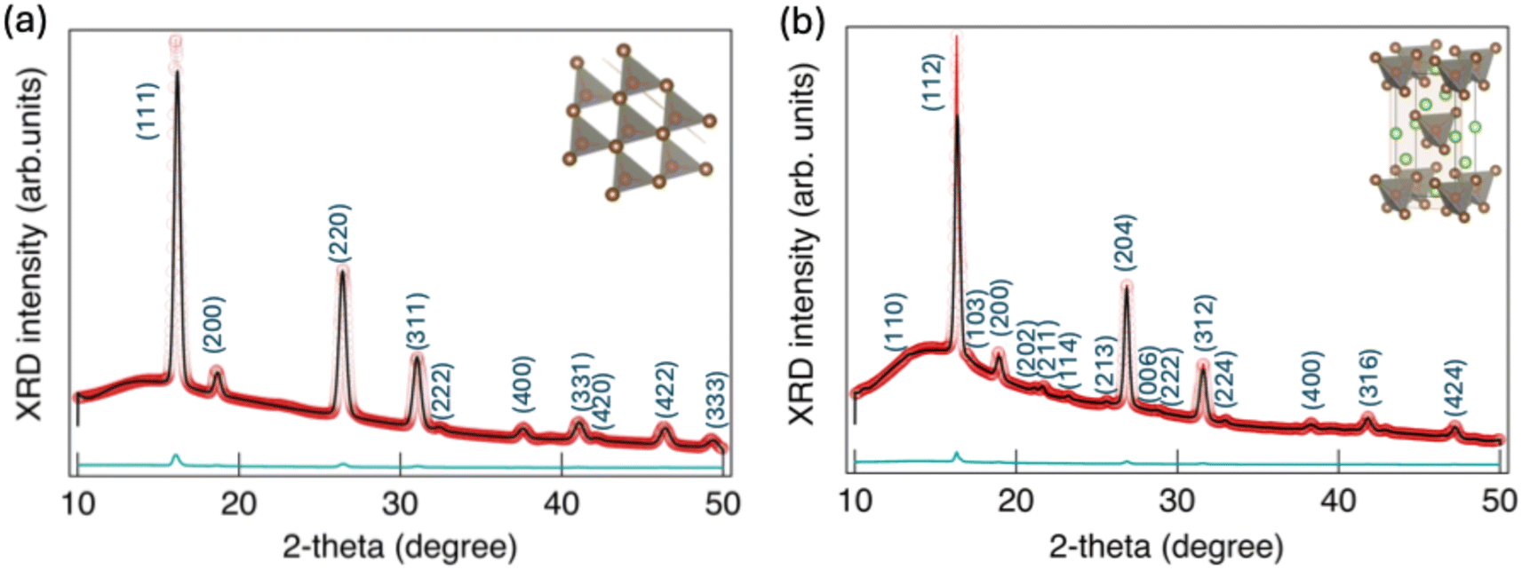
Among these predicted tellurides, several contain Zn, Ga and Te, together forming a (ZnTe)x(Ga2Te3)1−x family of materials with related tetrahedrally bonded crystal motifs. ZnTe, a II–VI compound, is usually formed in a cubic, zinc blende structure (Fig. 1a). Here, divalent Zn and hexavalent Te form an octet. On the other hand, Ga2Te3, containing trivalent Ga, is also based on tetrahedral atomic coordination motifs, but one third of the cation sites, i.e. gallium in Ga2Te3 are empty, generating disordered vacancy sites on the zinc blende lattice (Fig. 1c).23 The II–III2–VI4 compounds which are the focus of this paper, i.e. ZnGa2Te4, can be derived from these binary ZnTe and Ga2Te3 compounds. For example, ZnGa2Te4 has been observed in a vacancy-ordered zincblende-derived structure (Fig. 1b). Based on this observation, we propose that there exists an octet-conserving compositional tie-line, (ZnTe)x(Ga2Te3)1−x (0 ≤ x ≤ 1), where the relationship, built upon the zinc blende lattice, shown in Fig. 1d is conserved. This sum of valence electrons from Zn ([Ar] 3d104s2), Ga ([Ar] 3d104s24p1), and Te ([Kr] 4d105s25p4) is conserved at 96 valence electrons, and can be demonstrated through the following equations:| 12 ZnTe = 12 Zn(II) + 12 Te(VI) = 96 valence electrons |
| 3 ZnGa2Te4 = 3 Zn(II) + 6 Ga(III) + 3 VCation + 12 Te(VI) = 96 valence electrons |
| 4 Ga2Te3 = 8 Ga(III) + 4 VCation + 12 Te(VI) = 96 valence electrons |
 | ||
| Fig. 1 Crystal structure (a) zinc blende derived ZnTe (b) tetragonal ZnGa2Te4 (c) defective Ga2Te3 (d) chemical formulas and ternary phase diagram showing the compositional tie-line between zincblende-derived Zn-Ga-Te materials (ZnTe)x(Ga2Te3)1−x thin film growth. | ||
The II–III2–VI4 compounds can be characterized by tetrahedral cation-to-anion co-ordination, as an ordered vacancy compounds (Fig. 1b). Whenever all cation sites are tetrahedrally coordinated, tetragonal defective structures are formed.24 However, despite known structures, this suitable candidate material in this telluride family has never previously been experimentally investigated for CO2RR, and its further investigation is desirable.
Thin films of (ZnTe)x(Ga2Te3)1−x (where, x = 0 to 1) were synthesized on EXG glass substrates by RF combinatorial co-sputtering using ZnTe, Ga2Te3 and Te target precursors (see Experimental section). Deposition was carried out in an Ar atmosphere, with a substrate heater setpoint temperature of 200 °C. The whole combinatorial film was post-annealed at 500 °C by rapid thermal annealing (RTA) under atmospheric nitrogen pressure. Throughout this paper, we refer to these combinatorial films as (ZnTe)x(Ga2Te3)1−x, as they span the zincblende-derived compositional tie-line (Fig. 1d). However, note that Te concentration is a free variable which is at first in excess and then after annealing pins close to the targeted composition on the tie-line. A cubic to tetragonal phase transition has been observed upon changing cation–anion composition.
Fig. S1† shows the results of X-ray diffraction (XRD) patterns of as-deposited (ZnTe)x(Ga2Te3)1−x thin films with varying cation composition, measured by X-ray fluorescence (XRF). According to the XRD results, the as-deposited (ZnTe)x(Ga2Te3)1−x films (deposited at Tdep ∼200 °C) formed an amorphous/nanocrystalline Te phase with a wide range of elemental compositions (Zn/(Zn + Ga) = 0.20–0.95, Te ∼80%) (Fig. S1†). No Ga2Te3 or other secondary phases were observed in this growth condition. However, it is important to note that, when no extra Te target source was used, the as-deposited films become amorphous and peeled off on further annealing (Fig. S2†).
To convert the amorphous precursor into the product with desired zincblende-derived structure, we post-annealed the as-deposited film. After post-annealing the films at 300 °C for 5 minutes, partial crystallization was observed, characterized by the emergence of zinc blende ZnTe-like phases, although the Te phase remained predominant (Fig. S3†). Notably, no distinct Ga-containing secondary phases were detected at this stage. However, when the annealing temperature was increased to 500 °C, a structural transformation was observed, resulting in zincblende-derived ZnGa2Te4 structure as the main phase. Formation of a well-crystallized, phase-pure ZnGa2Te4 at higher annealing temperatures enhances structural ordering which is crucial for improved photoelectrochemical performance. Post-annealing helped to transform amorphous/Te nanocrystal structure into phase-pure cubic and tetragonal (ZnTe)x(Ga2Te3)1−x (Fig. 2a and b), depending on the anion and cation ratio. Within the composition range of Zn/(Zn + Ga) = 0.65–0.85 and ∼40% Te composition, all reflections in the XRD pattern can be indexed to cubic F3m symmetry. The tetragonal zincblende-derived structure in (ZnTe)x(Ga2Te3)1−x is observed across a range of cation stoichiometries ranging from 0.35–0.65, with Te fraction ∼50%. When the Zn/(Zn + Ga) ratio reaches ≥0.8, an unidentified peak emerges at approximately 2θ ≈ 35° (Fig. 2a – upper panel). It is interesting to see the tetragonal structure still emerges even though the annealed combinatorial films are Te-deficient. The fact that the Te concentration pre-and post-annealing straddles the tie-line of interest suggests that further iterative process optimization can be used to fine-tune the film composition. Formation of a well-crystallized, phase-pure ZnGa2Te4 at higher annealing temperature enhances structural ordering which is crucial for improved photoelectrochemical performance.
 | ||
| Fig. 2 Structural characterization (a) diffraction heatmap from post annealed samples (Tgrowth ∼500 °C) that exhibit the cubic (upper panel)–tetragonal (lower panel) crystal symmetry (λ = 1.54 Å) (b) ternary phase diagram showing the full composition of films (filled square and circle shape represents as-deposited sample and annealed samples, respectively) on EXG glass. Filled diamond shape (magenta) represent nominal stoichiometric ZnGa2Te4 composition. Other symbols represent the ZnGa2Te4 composition synthesized on FTO glass for photoelectrochemical measurement. | ||
The deposition temperature (Tdep) was varied from 200 °C to 300 °C (maintaining other deposition parameter same) to control the composition of volatile Zn and Te elements. The 200 °C growth temperature was optimal for achieving better crystallinity for the post-annealed ZnGa2Te4 thin film (Fig. S4†). This improvement is attributed to better composition control during sputter deposition.
Due to the high vapor pressure of Te, loss of Te increases with increasing deposition temperature. At deposition temperature of Tdep ∼300 °C, significant Te loss was observed during film growth (Zn:Ga:Te ∼ 12.9:28.3:58.7), compared to Tdep ∼200 °C (Zn:Ga:Te ≈ 6.3:11.6:81.9; Table S1†). This Te loss during deposition impacted the film crystallinity. At 300 °C, the crystallinity of ZnGa2Te4 film decreased, with amorphous/nano crystalline grains (Fig. S5c†). However, at Tdep ∼200–250 °C, the excess Te promoted diffusion and nucleation kinetics, enabling the formation of larger grains (∼120 nm; Fig. S5a and b†) with significantly improved crystallinity for vacancy-ordered zincblende-derived structure.
To further demonstrate the photoelectrochemical measurement, a uniform, stoichiometric, and phase-pure tetragonal film was prepared on FTO coated soda lime glass. To grow a uniform film on FTO glass, the deposition temperature was further decreased to 180 °C, which helps to maintain near stoichiometric condition for the post annealed samples. (Fig. 2b – filled diamond shape (grey)). A few calibration experiments were required (Fig. 2b open shapes, Table S2†) before achieving this final composition.
Structural characterization
To determine the phase purity of cubic and tetragonal structure, post-annealed combinatorial films were characterized by synchrotron grazing incidence wide angle X-ray scattering (GIWAXS) and integrated to generate a powder diffraction pattern. The experimental data and a LeBail whole pattern refinement against the reported F3m and I structure is presented in Fig. 3a and b, respectively, alongside the two crystal structure models. The fit returns lattice parameters for cubic structure of a = 6.09639 Å and for tetragonal structure of a = 5.94994 Å, c = 11.98607 Å.
 | ||
| Fig. 3 Wide-angle X-ray analysis integrated wide-angle X-ray scattering pattern along with a LeBail fit to the (a) cubic Ga:ZnTe and (b) tetragonal ZnGa2Te4 structure (here, black, red and cyan color represent calculated, experimental and difference spectrum of the refinement spectra) (λ = 0.97625 Å). | ||
To better understand the structural properties of ZnGa2Te4 thin films deposited on EXG glass substrate, (scanning) transmission electron microscopy ((S)TEM) analysis was carried out on a specimen prepared by focused ion beam (FIB) milling. Integrating across five selected area electron diffraction (SAED) patterns acquired from different locations along the TEM lamella (Fig. 4a) didn't produce an obvious ring pattern due to the relatively small sampling volume of SAED. However, 4D scanning transmission electron microscopy (4D-STEM) analysis was conducted to construct a virtual SAED pattern (Fig. 4b) by summing thousands of diffraction patterns across the film. This virtual SAED pattern shows more defined diffraction rings that align well with the ZnGa2Te4 structure, especially when comparing the azimuthally-integrated 1D experimental diffraction pattern with the simulated diffraction pattern from the ZnGa2Te4 structure (Fig. 4c). The (112), (224) and (204) planes of the tetragonal structure reflections can be assigned from 4D-STEM and are consistent with the XRD results. STEM energy-dispersive X-ray spectroscopy (EDS) was also performed to provide spatially resolved elemental information about the presence of Zn, Te and Ga elements within the film with large crystallized grains (Fig. 4d).
 | ||
| Fig. 4 Electron microstructure (a) TEM SAED pattern, (b) 4D-STEM virtual SAED (Bragg vector map) from the ZnGa2Te4 film, (c) experimental 1D diffraction pattern azimuthally integrated from 4D-STEM along with the simulated diffraction pattern, (d) STEM HAADF image and corresponding EDS elemental maps and (e) SEM top view of ZnGa2Te4 thin films. | ||
The composition of the film is as expected for ZnGa2Te4, though there is also an increased presence of oxygen at the film surface that could be attributed to oxidation occurring over time due to ambient exposure (Fig. S6†). Note that the tungsten (W) signal towards the film surface is from the protective W layer deposited during FIB preparation. There is also Ga present in the protective W layer, which comes from Ga implantation from the Ga-ion beam used for FIB preparation. We do not expect a significant amount of Ga implantation in the film or substrate because the final thinning of TEM lamella down to electron transparency was conducted using an Ar-ion beam. Quantitative EDS linescans (Fig. S6†) indicates an absence of Ga signal at film surface. Fig. 4e shows the top view scanning electron microscopy (SEM) image of corresponding ZnGa2Te4 absorber.
Electronic band structure calculations and optical property measurements
To gain atomistic insights into ZnGa2Te4 properties, we have performed first-principles calculations of ZnGa2Te4 electronic structure using the screened hybrid functional of Heyd–Scuseria–Ernzerhof (HSE06). As shown in Fig. 5a, the calculated band structure and density of states confirm that ZnGa2Te4 is a nearly direct bandgap semiconductor, with a bandgap of 1.86 eV. A strong presence of Te (p) states in the occupied region indicates that Te (p) orbitals play a dominant role in shaping the valence band. Meanwhile, the overlap of Te (p) and Ga (s) states near the Fermi level in the unoccupied region suggests that both elements contribute to the conduction band. This interaction is crucial for charge carrier dynamics, as it facilitates electron transition into the conduction band, which could influence the electronic and optoelectronic properties of the material. For ZnTe, both Te (p) and Zn (s) states contribute significantly to the valence and conduction bands (Fig. S7†). Fig. 5b shows that the computed optical absorption coefficient (α) of ZnGa2Te4 exceeds 105 cm−1, with an absorption onset at ∼1.8–1.9 eV, making it an efficient solar absorber.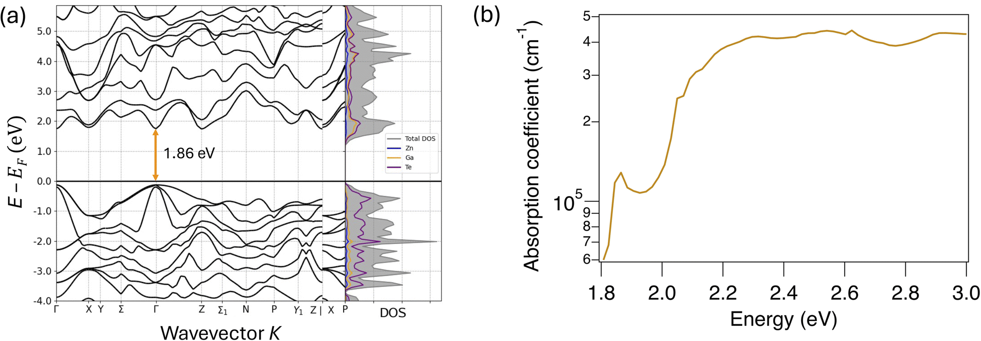 | ||
| Fig. 5 DFT calculation (a) electronic band structure of ZnGa2Te4 with total and element-resolved density of states (b) theoretically calculated absorption coefficient (α) for ZnGa2Te4. | ||
Further structural, optical, and PEC characterization has been conducted to evaluate the suitability of ZnGa2Te4 as a photocathode, comparing it with well known ZnTe films. Raman spectroscopy has been performed on cubic ZnTe/FTO and tetragonal ZnGa2Te4/FTO film, to further understand the structural changes from cubic to tetragonal phase conversion. As shown in Fig. 6a, for ZnTe, the peaks observed at 205, 410, 619 and 824 cm−1 could be assigned to first, second, third and fourth order longitudinal optical (LO) phonon scattering, respectively, which correspond to the cubic ZnTe structure.25 However, when Zn/(Zn + Ga) ratio reaches to ∼0.35 with Te fraction ∼47%, most of the LO phonon mode disappears. As ZnGa2Te4 structure resembles with tetragonal ZnGa2Se4 structure and in ZnGa2Se4, the most dominant A1 mode appears at 142.8 cm−1 for ZnGa2Se4, while for ZnGa2Te4 tetragonal structure, A1 mode appears ∼126.0 cm−1.26 The substitution of Se with Te should cause a shift of the peaks toward lower wavenumbers, primarily due to the incorporation of the heavier Te atom replacing Se atom.
 | ||
| Fig. 6 Optical characterization (a) Raman scattering – dashed line indicates the A1 vibrational mode for tetragonal ZnGa2Te4 (b) absorption coefficients (α(E)) spectra (inset is a photograph of uniform ZnGa2Te4 thin film on FTO substrate) (c) room-temperature PL spectra. | ||
The absorption spectra of ZnTe/FTO and ZnGa2Te4/FTO thin films were measured to investigate their optical properties. In Fig. 6b, ZnGa2Te4 shows absorption edges within ∼1.7–1.8 eV lower that 2.26 for ZnTe. The absorption coefficient is 105 cm−1, which is consistent with calculated results (Fig. 5b) and comparable to that of ZnTe. A defect center luminescence appeared around 1.70 eV for cubic ZnTe (Fig. 6c). This center luminescence in ZnTe could be attributed to a VZn- or some other donor defect complexes.27 Interestingly, 3 sharp peaks are identified in the high energy region ∼2.26 eV in PL spectra of ZnTe, which could be assigned as resonance Raman mode, as we observed longitudinal phonon modes in Raman spectra (Fig. 6a). These enhanced peaks could be interpreted as the multi-longitudinal optical phonon bands of cubic F3m structure enhanced by the near-bandedge PL band.28 However, no resonance peak was observed and PL peak emission was less intense for ZnGa2Te4 structure (Fig. 6c). The shift in the ZnGa2Te4 PL peak could be attributed to defect-induced emission. This less intense luminescence can be explained with the thicker ZnTe (∼350 nm) film compared to ZnGa2Te4 film (∼140 nm) (Table S2†).
Photogenerated carrier dynamics
To monitor the charge carrier dynamics of ZnGa2Te4/FTO film, TA spectroscopy has been performed across a range of time scales from picoseconds to microseconds. Fig. 7a and b shows TA spectra for different delay times for ZnGa2Te4 films on the picosecond and microsecond time scales. There is a fast initial evolution within 1 ps which may indicate ultrafast trapping but could also be thermalization of photoexcited carriers to the band edge.29 Beyond 1 ps, ZnGa2Te4 has a consistent spectrum throughout the 5 ns window, and even up to 1 μs. The TA spectra from 1–500 ps exhibits one broad absorbance peak centered at ∼1.80 eV, corresponding to the direct band to band transitions in ZnGa2Te4.30 This peak decays substantially on the picosecond time scale to reveal a photoinduced absorption with increased intensity at high energies. This evolution could be the resultant effect of trapped charges in various states with energies from deep state to band edge. Trap-mediated electron–hole recombination might be a significant loss pathway for ZnGa2Te4 based semiconductor which should be further optimized.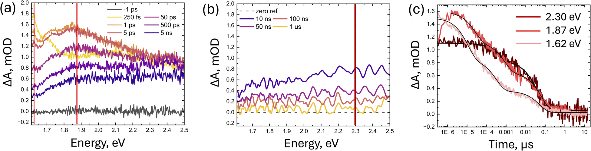 | ||
| Fig. 7 Carrier dynamics transient absorption spectra of ZnGa2Te4 photoexcited at 2.48 eV (100 nJ per pulse) at pump–probe delays spanning 250 fs–5 ns (a) and 10 ns–1 μs (b) TA kinetics measured at 2.30 eV (dark red), 1.87 eV (red), 1.62 eV (light red). Energies where kinetics were taken are indicated by the appropriately colored lines in panels (a) and (b). Kinetics were stitched together from the picosecond and microsecond experiments to show dynamics from 100 fs–10 μs (c). | ||
TA kinetics were extracted from both the pico- and micro second experiments and stitched together (Fig. 7c). Kinetics were extracted at a probe energy of 1.62 eV, 1.87 eV and 2.30 eV. At probe energy of 1.62 and 1.87 eV, they display similar kinetic decay trends with a complex decay kinetics, requiring tri-exponential function (τ1 ∼ 0.38 ± 0.026, τ2 ∼ 19.9 ± 0.935, and τ3 ∼ 566 ± 32.87 ps) to fit (Table S3†). These complex multiexponential components can be explained by trap-mediated pathways with different trap depths. This τ1 and τ2 can be correlated with the rapid relaxation of photoexcited electrons from the band edge to exciton-mediated trap states, while τ3 corresponds to the decay of dissociated free carriers occurring on a nanosecond timescale.31,32 The 0.38 ps decay in 1.62 eV is correlated with a growth at 1.87 eV. Although these features both appear as a positive ΔA, the growth at 1.87 eV may be related to loss of the ground state bleach which is superimposed on a photoinduced absorption, explaining the inverted shape of this feature. The signal at 2.30 eV does not decay in the picosecond window but matches dynamics at 1.87 eV after 1 ns (1000 ps). On the microsecond time scale, decay traces obtained at 2.30 eV are fit to two components (τ1 ∼ 0.04 ± 0.006, τ2 ∼ 0.65 ± 0.3 μs) (Table S4†).
Specifically, carrier lifetimes for ZnTe thin-film absorbers, which have been heavily researched, are similar. For our ZnTe sample, the transient absorption kinetics (spectrum not shown), at a probe energy of 1.70 eV also required fitting with a tri-exponential function, on picosecond time scale, yielding lifetimes of τ1 ≈ 5.5 ± 0.6, τ2 ≈ 61 ± 7.5, and τ3 ≈ 854 ± 97 ps, which are comparable to those observed in our ZnGa2Te4 films. Xiong et al. demonstrated that ZnTe films grown on FTO substrates by thermal evaporation exhibit complex charge carrier relaxation dynamics. Transient absorption spectroscopy (TAS) measurements, with decay traces recorded at 800 nm, were fitted using a tri-exponential model, yielding lifetimes of τ1 ≈ 2.6 ± 0.2, τ2 ≈ 24.5 ± 2.5, and τ3 ≈ 363 ± 32 ps.33 It is important to study and optimize these photoexcited carrier relaxation process of ZnGa2Te4, to enhance the migration of charge carriers for photocatalytic reactions.
Photoelectrochemical properties
Mott–Schottky analyses at four different frequencies were carried out in CO2-bubbled 0.1 M KHCO3 solution (pH 6.8) to experimentally characterize the energy band positions of ZnTe and ZnGa2Te4, and the resulting plot is shown in Fig. 8a. The negative slope in the Mott–Schottky plot indicates both ZnTe and ZnGa2Te4 are p-type semiconductors. Flat band potential (EFb) is estimated from the x-axis intercepts of Mott–Schottky plot and is determined to be 1.07 V and 0.7 V vs. Ag/AgCl (or −5.71 and −5.34 eV) for ZnTe and ZnGa2Te4, respectively. For a p-type semiconductor, the flat band potential approximates the valence band edge potential (VB) under flat band conditions and these measured VBs agree well with the theoretically predicted ones.17 With the known band gap energy discussed earlier, the conduction band (CB) edges are calculated to be −3.45 and −3.48 eV for ZnTe and ZnGa2Te4, respectively (Fig. 8b). According to the reported potentials for CO2R,17 the CB position of ZnTe and ZnGa2Te4 are less negative than the electrochemical CO2 conversion to CH4 (−4.2 eV), CH3OH (−4.04 eV), HCHO (−3.96 eV), CO (−3.91 eV), and HCOOH (−3.83 eV). While these band positions can cause simultaneous competing hydrogen evolution reaction (HER), the two photocathodes investigated in the present work are capable of reducing CO2 under illuminations. | ||
| Fig. 8 Mott–Schottky analysis (a) energy band position characterization for ZnTe and ZnGa2Te4. Measurements are carried out in CO2-bubbled 0.1 M KHCO3 (pH = 6.8) and at multiple frequencies to validate the measured flat band potentials. (b) Band potentials and bandgap energy for ZnTe and ZnGa2Te4. | ||
The chopped (dark/light) linear scanning voltammetry (LSV) scans of the ZnGa2Te4 and ZnTe thin-film photo cathodes are presented in Fig. 9a, b, S8a and b,† respectively. The HT-ANEC instrument with fiber-optic-coupled photodiodes for front side illumination is used to evaluate the performance of photocathodes investigated in this study.34 To achieve higher photocurrents for accurate and reliable quantifications of CO2RR product, we used a high energy LED at 455 nm (∼2.70 eV within the visible light region) to compare these two photocathodes. ZnTe and ZnGa2Te4 compounds displays similar photocurrent over the entire operating potential range and reach a photocurrent density close to −2 mA cm−2 at −1.0 V vs. reversible hydrogen electrode (RHE) (Fig. 9a and S8a†). As the bandgap of these two are determined to be ∼1.86 and ∼2.26 eV, respectively, and the energy band position characterized by Mott–Schottky above shows both are suitable for PEC CO2R and HER, the 2.70 eV LED has photon energy higher than the bandgaps of both ZnGa2Te4 and ZnTe, which could contribute to their similar photocurrents. For ZnGa2Te4, however, only the near stoichiometric but slightly Te-rich sample shows both high photocurrents and negligible dark currents. Other off-stoichiometric, Te-poor samples do not show such promising PEC results (Fig. S9 and Table S2†). It is noted that all samples, including both ZnTe and ZnGa2Te4 have a reductive current between −0.25 and −0.6 V vs. RHE, but present only in the 1st cycle of the cathodic sweep. These reductive currents could be caused by reduction of residues on the surface (e.g., ZnOx, GaOx, or TeOx).
 | ||
| Fig. 9 Photoelectrochemical performance CV results under 455 nm LED illumination (a) without additive and (b) with additive, and (c) CAs at multiple potentials without additive (1st bars; truncated) and with additive (2nd bars; square) for ZnGa2Te4 photocathodes. | ||
CV scans with a white LED (Doric dual LED, LEDC2-W35_SMA, Fig. S10†) providing broad spectrum illumination was also used to compare the performance of ZnGa2Te4 and ZnTe. In contrast to illumination under 455 nm (2.70 eV), ZnGa2Te4 which possess a narrower bandgap (ZnGa2Te4vs. ZnTe: 1.86 vs. 2.26 eV) shows significant photocurrents over the entire CV scan range (Fig. S11†). The additional lower energy photons from the white LED compared to 455 nm LED (i.e. >455 nm) suggest ZnGa2Te4 absorbs visible light below the bandgap energy of ZnTe.
Chronoamperometry (CA) at multiple potentials following cyclic voltammetry (CV) was conducted to reveal products formed (Fig. 9c and S8c† – left side bars). The products accumulated during CA measurements were analyzed by GC and HPLC in the HT-ANEC system. Results show that both ZnTe and ZnGa2Te4 produce only H2 at lower applied bias (less than −0.4 V vs. RHE). At higher applied bias (>−0.6 V vs. RHE), both photocathodes start to produce C1 products (including carbon monooxide, CO and formate, HCOOH) in addition to H2. ZnGa2Te4 shows FE of CO2RR less than 10% while ZnTe sample shows >20%. Ga has been reported to be a HER catalyst.35,36 In contrast, Zn is known as an efficient catalyst for reducing CO2 into CO and HCOOH. More specifically, Zn-rich surfaces on ZnTe have been reported to not only facilitate the charge transfer but also acts as an electrocatalyst to enhance the selectivity for carbon products.37 The substitution of Ga for Zn in ZnGa2Te4 could be responsible for the decrease in CO2RR and increase in HER selectivity. Nevertheless, increasing applied bias increases CO2RR selectivity on both photocathodes.
The effects of organic additives
Motivated by our previous study, 10 mM additive diaryliodonium has been included in the electrolyte for ZnTe and ZnGa2Te4 CO2RR investigations.13,16 The first cycle of CV scans shows reductive currents at very positive potentials (Fig. 9b and S8b†). This could result from polymerization/deposition of additives onto the electrode surface, since they don't occur in subsequent cycles. Due to illumination by 2.7 eV LED, which is higher than the bandgaps of both materials, ZnTe and ZnGa2Te4 show similar photocurrents in the presence of additives, as observed above with no additives present. The additive, however, results in slightly decreased photocurrents compared to the no additive environment for both electrodes.When the additive diaryliodonium is present in the electrolyte, ZnTe shows a moderate enhancement of CO2RR selectivity at the potentials where CO2RR occurred along with suppression of HER (Fig. S8c† – right side bars). This change agrees with previously reported effects of additives on ZnTe PEC CO2RR performance.16 Interestingly, the addition of additive greatly increases FE of CO2RR including CO and HCOOH on ZnGa2Te4 from ≤10% to ∼50% with suppression of HER (Fig. 9c – right side bars). This CO2RR selectivity enhancement upon addition of additives makes its performance comparable to that of ZnTe under 455 nm (i.e. 2.70 eV) illumination conditions. The photocurrent values and corresponding product distributions for each CA experiment are summarized in Table S5.†
The organic additive has been shown to reduce and dimerize/oligomerize into a nonconductive layer on the electrode surface to enhance CO2RR product selectivity.38 It was reported that the diaryliodonium additive may help increase CO2RR selectivity not just by suppressing HER but could further increase CO2RR catalytic activity. It boosts the partial current density of CO2RR sufficiently to maintain total current density not only for dark electrolysis on Cu-based electrodes but also for PEC on photocathodes ZnTe.13,39,40 Mechanisms proposed to account for the change in selectivity include slow diffusion of proton carriers to the electrode, lower H2O and increased CO2 concentration within the films, nanostructuring of the electrode, and interactions of CO2 reduction intermediates on the electrode with the film.41,42 For the diaryliodonium additive specifically, rotating-disk-electrode (RDE) studies from Watkins et al.39 indicate that the film acts as a barrier toward the diffusion of proton sources to the electrode surface, supporting that decreased proton availability near the electrode surface suppresses HER. The grafted film from diaryliodonium grows perpendicular to the electrode surface and creates a low-density film with channels, enabling facile substrate transport through the film and maintaining catalytic activity. The observed slightly lower photocurrents from our tests could be due to the attenuation of incident light intensity by the additives.
The reduced bandgap of ZnGa2Te4 (i.e. ∼1.86 eV), which is in the range needed for PEC applications should facilitate visible light absorption from the solar spectrum. SEM image shows grain size ∼120 nm for ZnGa2Te4 but for ZnTe grain size less than 60 nm (Fig. S12a and b†). Larger grain size facilitates efficient charge transport, with less recombination, thereby enhancing photoelectrochemical (PEC) performance. Also, we determined roughness of the (ZnTe, ZnGa2Te4)/FTO film using AFM, which shows the root-mean-square (RMS) surface roughness of the ZnGa2Te4 and ZnTe film around ∼11.2 nm and ∼9.7 nm, respectively (Fig. S13a and b†). These properties contribute to efficient PEC activity of ZnGa2Te4 (Fig. 9 and S11†). With the assistance of organic additives to increase its CO2RR selectivity, CO2RR performance of ZaGa2Te4 becomes comparable to, and even surpasses, that of the widely investigated ZnTe.
Long-term photoelectrochemical stability
Inductively coupled plasma mass spectrometry (ICP-MS) was performed on post-reaction electrolytes to quantify corrosion from the electrode into solution. X-ray fluorescence (XRF) measurements on the electrode surface were performed pre- and post-PEC to confirm the changes in elemental molar loadings of the electrode. Fig. S14† shows ZnTe does not show noticeable corrosion under the conditions used for the PEC measurements. XRF confirms the pre- and post-run composition (Table S6†) barely changes, in agreement with previous reports.16 ZnGa2Te4 shows minimal Zn and Te loss at all potentials. As each photocathode was first tested at −0.2 V, the relatively high concentrations of elements seen at −0.2 V is likely due to reduction of surface oxides. Nevertheless, increasing Ga corrosion was observed with increasing applied bias. Theoretical prediction17 suggests that this ZnGa2Te4 could be stable up to −0.5 V vs. RHE. The HT-ANEC measurement is 15 min at each potential.To further understand how this corrosion of Ga could influence the performance of ZnGa2Te4 in PEC CO2R, we conducted a longer PEC measurement using a conventional H-cell setup without additive at −0.8 V vs. RHE. To produce photocurrent densities consistent with prior HT-ANEC measurements with the white LED, and to assure sufficient photocurrent for reliable product quantification, a mercury–xenon lamp calibrated for 3-sun illumination intensity was used (Fig. S10b†). Fig. 10a shows that the photocurrent of ZnGa2Te4 remained stable over the entire measurement. The product selectivity generally agrees with that from HT-ANEC measurements at this potential, with H2 as the major product and with minor CO and formate product formation. It is noted that formic acid could only be analyzed after the longer duration measurement concluded and the value shown is the average over the entire test period. CO increases initially and levels out at ∼10%.
 | ||
| Fig. 10 (a) Stability test of ZnGa2Te4 without additives using a traditional H-cell at −0.8 V vs. RHE with periodic headspace measurements. Note that formate shown in the figure is the average over entire measurement. (b) Corrosion study by ICP-MS and XRF for pre-and post-PEC run samples. | ||
ICP-MS, as well as XRF characterization, was carried out after the H-Cell PEC measurement (Fig. 10b). Similar to HT-ANEC measurements, corrosion occurs, especially for Ga, and this loss may be responsible for the slight increase in CO production at the beginning of the measurement. Interestingly, the dissolved metal concentrations including Zn, Ga, and Te from this 180 min measurement are very similar to those of the 15 min HT-ANEC measurements. This suggests the corrosion mostly occurs at the beginning of PEC and the dissolved metals concentration at the given electrochemical potential and pH reaches equilibrium,43 consistent with the observed relatively stable photocurrents and product formation.
Conclusion
By introducing the Te rich synthesis route, we have successfully synthesized thin films of a telluride material, ZnGa2Te4 with tetragonal structure, as a photocathode for PEC CO2RR. The structural, optical, and photoelectrochemical properties of the tetragonal ZnGa2Te4 films were systematically investigated. Its suitable direct bandgap of 1.86 eV and relatively high carrier lifetime measured by transient absorption spectroscopy makes this thin film absorber a promising candidate for photocathode applications. With a stable current density of approximately −2 mA cm−2, this material is an interesting candidate for further study. There are many opportunities to improve this ZnGa2Te4 photocathode performance by varying the structure, morphology and defect properties, we demonstrate that its CO2RR selectivity can be strongly enhanced by organic additives. Overall, this work demonstrates the successful synthesis of ZnGa2Te4 thin film as a potential photoelectrode for PEC CO2R application.Experimental section
Synthesis
The Zn–Ga–Te phase space was explored using combinatorial radio-frequency (RF) cosputtering methods. The chamber base pressure was 1 × 10⁻⁸ torr prior to depositions. During depositions, the pressure was maintained at 2.7 mTorr with 16 sccm Ar. Substrates were clamped to platens heated by a serpentine SiC resistance coil. Following a period of pre-sputtering, the combinatorial alloy films were deposited for 90 minutes at 200 °C on EXG glass.(ZnTe)x(Ga2Te3)1−x thin films were synthesized by radio frequency (RF) co-sputtering from alloyed 50.8 mm diameter ZnTe and Ga2Te3 targets, and one Te target, with ZnTe and Ga2Te3 power density of 0.74 and 2.22 W cm−2, respectively, and Te 0.49 W cm−2 in a Ar gas environment. All the films were annealed in RTA at 500–550 °C in N2 environment for 5 minutes. However, to grow uniform film on EXG and FTO, substrate temperature was fixed 200 and 180 °C, respectively. Target power density was optimized for uniform ZnGa2Te4 structure.
ZnTe films were grown by RF sputtering of ZnTe target and deposited on FTO glass substrate. Substrate was deposited at 170 °C temperature for 70 min, and followed by annealing at ∼435 °C.
Characterization
A 455 nm LED (Thorlabs M455F3) was selected as a major light source in this report because (1) it has higher energy than the band gap of both ZnGa2Te4 and ZnTe is in the range of visible light, not ultraviolet, and (2) could generate greater photocurrents for more accurate product quantifications by GC and HPLC. A LED with white light (intensity ∼6.94 mW cm−2) spectrum was also used in some cases (Fig. S10†) to distinguish the PEC performance between the two materials in the broad visible light regions. We performed multipotential measurements (by CA) following CV (i.e. CA and CV was on two different sample spots) to investigate the CO2 RR product distribution. We carried out CA measurements in the order −0.2, −0.4, −0.6, −0.8, and −1 V vs. RHE for 15 min (900 s) unless the film mechanically delaminates. The light was on for the first 882 s and then shut off for the rest 18 s. The ending 18 s under the dark provides the baseline for calculating J_photo and J_FE and can be used to evaluate if dark currents exist due to any film delaminations (the substrate is FTO and could show electrochemical activity at the potential range used in this report). The high-throughput analytical electrochemistry (HT-ANEC) instrument34 we used to test CO2RR performance requiring rapid flow to generate suitable and reproducible mass transport conditions. The rapid flow could cause the predeposited additive film to delaminate over time. For the tests with additive, the electrolyte contained additives at all times to ensure that the film remains on the electrode; hence, the thickness of diaryliodonium is not directly controlled. For this initial study, we focus on the discovery of the combined improvement in selectivity and activity. The impact of diaryliodonium thickness on stability and selectivity optimization will be the subject of future work. At the end of each (photo)electrolysis, we sampled gaseous and liquid products by the robotic sample handling system and was analyzed by gas chromatography (GC; Thermo Scientific TRACE 1300) and high-performance liquid chromatography (Thermo Scientific UltiMate 3000), respectively. Detailed product detection methods are can be found at our previous publication.34
For PEC CO2 reduction measurements in an H-Cell, the cathode had an area of 1 cm2. CO2 saturated 0.10 M potassium bicarbonate without additive was used as the electrolyte. A Pt foil anode was used behind a bipolar membrane (Fumasep® FBM single film, Fumatech) membrane. A leakless Ag/AgCl electrode was used as a reference electrode. A mercury–xenon lamp calibrated for 3-sun illumination intensity was used (Fig. S10b†). Carbon dioxide was provided to the electrochemical cell at a flow rate of 5 sccm using an Alicat flow controller. The gas exhaust stream of the electrochemical cell was passed through a liquid trap before flowing through the gas sampling loop of an Agilent 7820a GCMS/TCD with an Alicat flow meter connected to its exhaust.
Data availability
The data supporting this article have been included as part of the ESI.†Author contribution
Conceptualization, S. Q., S. R. B., and A. Z.; methodology, S. Q., S. R. B., and A. Z.; investigation, S. Q., Y. C. L., M. G., J. M., W. Z., R. Y., M. A., C. P. M., S. R. B.; writing—original draft, S. Q. writing—reviewing and editing, S. Q., Y. C. L., M. G., J. M., W. Z., S. R. B., A. Z. and all co-authors; funding acquisition A. Z., K. P., J. H.; supervision A. Z.Conflicts of interest
The authors declare no conflict of interest.Acknowledgements
This work was authored in part by the National Renewable Energy Laboratory for the U.S. Department of Energy (DOE) under contract no. DE-AC36-08GO28308. Funding provided by the Liquid Sunlight Alliance, which is supported by the U.S. Department of Energy, Office of Science, Office of Basic Energy Sciences, Fuels from Sunlight Hub under award number DE-SC0021266. Use of the Stanford Synchrotron Radiation Lightsource, SLAC National Accelerator Laboratory, is supported by the U.S. DOE, Office of Science, Office of Basic Energy Sciences under Contract No. DE-AC02-76SF00515. Thanks to Dr Nicholas Strange for support with GIWAXS measurements. The views expressed in the article do not necessarily represent the views of the DOE or the U.S. Government.References
- M. Grätzel, Photoelectrochemical cells, Nature, 2001, 414(6861), 338–344 CrossRef PubMed.
- K. Sivula and R. Van De Krol, Semiconducting materials for photoelectrochemical energy conversion, Nat. Rev. Mater., 2016, 1(2), 1–16 Search PubMed.
- D. Li, et al., Powering the world with solar fuels from photoelectrochemical CO2 reduction: basic principles and recent advances, Adv. Energy Mater., 2022, 12(31), 2201070 CrossRef CAS.
- L. K. Putri, et al., Toward excellence in photocathode engineering for photoelectrochemical CO2 reduction: Design rationales and current progress, Adv. Energy Mater., 2022, 12(41), 2201093 CrossRef CAS.
- J. W. Beeman, et al., Si photocathode with Ag-supported dendritic Cu catalyst for CO 2 reduction, Energy Environ. Sci., 2019, 12(3), 1068–1077 RSC.
- M. Xia, et al., Efficient Cu2O Photocathodes for Aqueous Photoelectrochemical CO2 Reduction to Formate and Syngas, J. Am. Chem. Soc., 2023, 145(51), 27939–27949 CrossRef CAS PubMed.
- K. Tian, et al., Lattice Distortion Promotes Carrier Separation to Improve the Photoelectrochemical Water Splitting Performance of Bismuth Vanadate Photoanode, Adv. Funct. Mater., 2024, 2410548 CrossRef CAS.
- A. L. Greenaway, et al., Zinc titanium nitride semiconductor toward durable photoelectrochemical applications, J. Am. Chem. Soc., 2022, 144(30), 13673–13687 CrossRef CAS PubMed.
- X. Han, et al., Photothermal CO2 hydrogenation to CO on CeO2 catalyst via redox mechanism, Chem. Eng. J., 2025, 510, 161609 CrossRef CAS.
- W. Huang, et al., Highly selective CO2 conversion to CH4 by a N-doped HTiNbO5/NH2-UiO-66 photocatalyst without a sacrificial electron donor, JACS Au, 2024, 5(3), 1184–1195 CrossRef PubMed.
- Y. Liu, et al., Photoelectrochemical CO2 Reduction at a Direct CuInGaS2/Electrolyte Junction, ACS Energy Lett., 2023, 8(4), 1645–1651 CrossRef CAS.
- S. Zhou, et al., Accelerating Electron-Transfer and Tuning Product Selectivity Through Surficial Vacancy Engineering on CZTS/CdS for Photoelectrochemical CO2 Reduction, Small, 2021, 17(31), 2100496 CrossRef CAS PubMed.
- Y. Lai, et al., Molecular coatings improve the selectivity and durability of CO2 reduction chalcogenide photocathodes, ACS Energy Lett., 2022, 7(3), 1195–1201 CrossRef CAS.
- J. W. Jang, et al., Aqueous-solution route to zinc telluride films for application to CO2 reduction, Angew. Chem., Int. Ed., 2014, 53(23), 5852–5857 CrossRef CAS PubMed.
- G. Zeng, et al., Surface Composition Impacts Selectivity of ZnTe Photocathodes in Photoelectrochemical CO2 Reduction Reaction, ACS Energy Lett., 2024, 10, 34–39 CrossRef PubMed.
- C. P. Muzzillo, et al., Chloride Treatments Improve Zinc Telluride Absorbers for Photoelectrochemical Carbon Dioxide Reduction, ACS Appl. Energy Mater., 2025, 8(2), 983–990 CrossRef CAS PubMed.
- A. K. Singh, et al., Robust and synthesizable photocatalysts for CO2 reduction: a data-driven materials discovery, Nat. Commun., 2019, 10(1), 443 CrossRef CAS.
- M. Siron, O. Andriuc and K. A. Persson, Data-driven investigation of tellurium-containing semiconductors for CO2 reduction: trends in adsorption and scaling relations, J. Phys. Chem. C, 2022, 126(31), 13224–13236 CrossRef CAS.
- T. Biswas and A. K. Singh, Excitonic effects in absorption spectra of carbon dioxide reduction photocatalysts, npj Comput. Mater., 2021, 7(1), 189 CrossRef CAS.
- G. Kühn, et al., Preparation, structure, and infrared lattice vibrations of LiInTe2, Z. Anorg. Allg. Chem., 1985, 531(12), 61–66 CrossRef.
- S. Ozaki, K.-i. Muto and S. Adachi, Optical properties and electronic band structure of CdGa2Te4, J. Phys. Chem. Solids, 2003, 64(9–10), 1935–1939 CrossRef CAS.
- S. Fouad, et al., Structural characterization and novel optical properties of defect chalcopyrite ZnGa2Te4 thin films, Mater. Res. Bull., 2011, 46(11), 2141–2146 CrossRef CAS.
- C. Julien, et al., Optical and electrical properties of Ga2Te3 crystals, Phys. Status Solidi A, 1994, 145(1), 207–215 CrossRef CAS.
- F. J. Manjon, I. Tiginyanu and V. Ursaki, Pressure-Induced Phase Transitions in AB2X4 Chalcogenide Compounds, Springer, 2014 Search PubMed.
- Q. Zhang, et al., Exciton-phonon coupling in individual ZnTe nanorods studied by resonant Raman spectroscopy, Phys. Rev. B: Condens. Matter Mater. Phys., 2012, 85(8), 085418 CrossRef.
- R. Vilaplana, et al., High-pressure Raman scattering study of defect chalcopyrite and defect stannite ZnGa2Se4, J. Appl. Phys., 2013, 113(23), 233501 CrossRef.
- C. Norris, The origin of the 1.59-eV luminescence in ZnTe and the nature of the postrange defects from ion implantation, J. Appl. Phys., 1982, 53(7), 5172–5176 CrossRef CAS.
- F. Iida, et al., Resonant raman peaks of ZnTe grown by MBE, Phys. Status Solidi B, 1994, 183(2), K75–K78 CrossRef CAS.
- H. Liu, et al., Measuring photoexcited electron and hole dynamics in ZnTe and modeling excited state core-valence effects in transient extreme ultraviolet reflection spectroscopy, J. Phys. Chem. Lett., 2023, 14(8), 2106–2111 CrossRef CAS PubMed.
- P. Wen, et al., A colloidal ZnTe quantum dot-based photocathode with a metal–insulator–semiconductor structure towards solar-driven CO 2 reduction to tunable syngas, J. Mater. Chem. A, 2021, 9(6), 3589–3596 RSC.
- H. Sun, et al., Structure defects promoted exciton dissociation and carrier separation for enhancing photocatalytic hydrogen evolution, Appl. Catal., B, 2020, 264, 118480 CrossRef.
- H. Wang, et al., Oxygen-vacancy-mediated exciton dissociation in BiOBr for boosting charge-carrier-involved molecular oxygen activation, J. Am. Chem. Soc., 2018, 140(5), 1760–1766 CrossRef CAS PubMed.
- X. Xianqiang, F. Mark and X. Yiming, Time-Resolved Spectroscopy of ZnTe Photocathodes for Solar Fuel Production, J. Phys. Chem. C, 2017, 121(40), 22073–22080 CrossRef.
- R. J. Jones, et al., Reactor design and integration with product detection to accelerate screening of electrocatalysts for carbon dioxide reduction, Rev. Sci. Instrum., 2018, 89(12) CrossRef CAS PubMed.
- W. Luo, et al., Boosting CO production in electrocatalytic CO2 reduction on highly porous Zn catalysts, ACS Catal., 2019, 9(5), 3783–3791 CrossRef CAS.
- X. Li, et al., Cocatalysts for selective photoreduction of CO2 into solar fuels, Chem. Rev., 2019, 119(6), 3962–4179 CrossRef CAS.
- G. Zeng, et al., Surface Composition Impacts Selectivity of ZnTe Photocathodes in Photoelectrochemical CO2 Reduction Reaction, ACS Energy Lett., 2024, 10(1), 34–39 CrossRef PubMed.
- W. Nie, et al., Organic additive-derived films on Cu electrodes promote electrochemical CO2 reduction to C2+ products under strongly acidic conditions, Angew. Chem., Int. Ed., 2023, 62(12), e202216102 CrossRef CAS PubMed.
- N. B. Watkins, et al., In situ deposited polyaromatic layer generates robust copper catalyst for selective electrochemical CO2 reduction at variable pH, ACS Energy Lett., 2022, 8(1), 189–195 CrossRef.
- C. L. Chevalier and E. C. Landis, Electrochemical attachment of diazonium-generated films on nanoporous gold, Langmuir, 2015, 31(31), 8633–8641 CrossRef CAS.
- A. Thevenon, et al., Dramatic HER suppression on Ag electrodes via molecular films for highly selective CO2 to CO reduction, ACS Catal., 2021, 11(8), 4530–4537 CrossRef CAS.
- A. Thevenon, et al., In-situ nanostructuring and stabilization of polycrystalline copper by an organic salt additive promotes electrocatalytic CO2 reduction to ethylene, Angew. Chem., 2019, 131(47), 17108–17114 CrossRef.
- L. Zhou, et al., Stability and activity of cobalt antimonate for oxygen reduction in strong acid, ACS Energy Lett., 2022, 7(3), 993–1000 CrossRef CAS.
- L. A. Giannuzzi, et al., Applications of the FIB lift-out technique for TEM specimen preparation, Microsc. Res. Tech., 1998, 41(4), 285–290 CrossRef CAS PubMed.
- B. H. Savitzky, et al., py4DSTEM: A software package for four-dimensional scanning transmission electron microscopy data analysis, Microsc. Microanal., 2021, 27(4), 712–743 CrossRef CAS PubMed.
- R. Hovden, et al., The open-source cornell spectrum imager, Microsc. Today, 2013, 21(1), 40–44 CrossRef CAS.
- J. Schindelin, et al., Fiji: an open-source platform for biological-image analysis, Nat. Methods, 2012, 9(7), 676–682 CrossRef CAS PubMed.
- G. Kresse and J. Furthmüller, Efficient iterative schemes for ab initio total-energy calculations using a plane-wave basis set, Phys. Rev. B: Condens. Matter Mater. Phys., 1996, 54(16), 11169 CrossRef CAS PubMed.
- S. P. Ong, et al., Python Materials Genomics (pymatgen): A robust, open-source python library for materials analysis, Comput. Mater. Sci., 2013, 68, 314–319 CrossRef CAS.
- A. Ganose, Atomate2: Modular workflows for materials science, ChemRxiv, 2025, preprint, pp. 1–66, DOI:10.26434/chemrxiv-2025-tcr5h.
- A. S. Rosen, et al., Jobflow: Computational workflows made simple, J. Open Source Softw., 2024, 9(93), 5995 CrossRef.
- A. Jain, et al., The Materials Project: a materials genome approach to accelerating materials innovation, APL Mater., 2013, 1, 011002 CrossRef.
- J. P. Perdew, K. Burke and M. Ernzerhof, Generalized gradient approximation made simple, Phys. Rev. Lett., 1996, 77(18), 3865 CrossRef CAS PubMed.
- J. W. Furness, et al., Accurate and numerically efficient r2SCAN meta-generalized gradient approximation, J. Phys. Chem. Lett., 2020, 11(19), 8208–8215 CrossRef CAS.
- J. Heyd, G. E. Scuseria and M. Ernzerhof, Hybrid functionals based on a screened Coulomb potential, J. Chem. Phys., 2003, 118(18), 8207–8215 CrossRef CAS.
- M. Marsman, et al., Hybrid functionals applied to extended systems, J. Phys.: Condens. Matter, 2008, 20(6), 064201 CrossRef CAS.
- R. X. Yang, et al., High-throughput optical absorption spectra for inorganic semiconductors, arXiv, 2022, preprint, arXiv:2209.02918, DOI:10.48550/2209.02918.
Footnote |
| † Electronic supplementary information (ESI) available. See DOI: https://doi.org/10.1039/d5ta02891d |
| This journal is © The Royal Society of Chemistry 2025 |