
 Open Access Article
 This Open Access Article is licensed under a Creative Commons Attribution-Non Commercial 3.0 Unported Licence
Harnessing self-powered and photoresponsive biomechanical activity sensors by exploring the piezo-phototronic effect in lead-free layered halide perovskite/PVDF composites†
Prabhat
Kumar
 a,
Tufan
Paul
a,
Aditi
Sahoo
a,
Manoj
Singh
a,
Arupjyoti
Pathak
b,
Ranjit
Thapa
bc and
Rupak
Banerjee
*ad
a,
Tufan
Paul
a,
Aditi
Sahoo
a,
Manoj
Singh
a,
Arupjyoti
Pathak
b,
Ranjit
Thapa
bc and
Rupak
Banerjee
*ad
aDepartment of Physics, Indian Institute of Technology Gandhinagar, Palaj 382355, Gujarat, India. E-mail: rupakb@iitgn.ac.in
bDepartment of Physics, SRM University AP, Amaravati 522240, Andhra Pradesh, India
cCentre for Computational and Integrative Sciences, SRM University-AP, Amaravati 522240, Andhra Pradesh, India
dK C Patel Centre for Sustainable Development, Indian Institute of Technology Gandhinagar, Palaj 382355, Gujarat, India
First published on 6th May 2025
Abstract
Developing flexible, wearable, efficient, and self-powered electronic devices based on piezoelectric nanogenerators aspires to be a sustainable solution to renewable energy harvesting and storage. We report on a lead-free halide perovskite Cs3Sb2I9 and polyvinylidene fluoride (PVDF) based composite device capable of scavenging energy from routine biomechanical activities. Regulated incorporation and optimization of Cs3Sb2I9 into the PVDF matrix increased the electroactive phase of the device to ∼82% with a piezoelectric coefficient of 7.48 pm V−1. The champion device produced an open circuit output voltage of 85 V and a current of 2.6 μA. Furthermore, the device generated approximately ∼1.26 μW cm−2 of power density when connected to a 0.8 MΩ resistor, sufficient to operate portable electronic gadgets. We tested the device for its energy generation capabilities under simple human biomechanical movements such as hand hammering, finger tapping, elbow bending, knee bending, and toe pressing. To demonstrate the versatility of the nanogenerator device, we also tested its energy generation and storage capabilities by charging capacitors up to ∼2.2 V. The device exhibited impressive durability and repeatability over 10![[thin space (1/6-em)]](https://www.rsc.org/images/entities/char_2009.gif) 000 cycles, underscoring its potential as a promising solution for addressing the energy demand of portable and Internet of Things (IoT) devices through piezoelectric nanogenerators. Work function calculations using density functional theory demonstrated that the composite exhibited a reduced work function compared to individual components, indicating favorable electron emission characteristics. We also realized the piezo-phototronic effect in the composite using a self-powered photodetector, which exhibited an increment of 63% in the photocurrent, offering potential for piezotronic and optoelectronic devices.
000 cycles, underscoring its potential as a promising solution for addressing the energy demand of portable and Internet of Things (IoT) devices through piezoelectric nanogenerators. Work function calculations using density functional theory demonstrated that the composite exhibited a reduced work function compared to individual components, indicating favorable electron emission characteristics. We also realized the piezo-phototronic effect in the composite using a self-powered photodetector, which exhibited an increment of 63% in the photocurrent, offering potential for piezotronic and optoelectronic devices.
1. Introduction
The ever-increasing demand for energy and the strained resources of traditional energy necessitate the development of self-powered electronic devices for efficient and sustainable energy sources, which is consequently an important focus area of global research. Environment protection and sustainable energy sources are the two main pillars of our future world, and much research has been undertaken to harness various types of renewable energy resources, including solar, thermal, mechanical, wind, and vibration.1,2 In this context, the halide perovskites (e.g., CsPbBr3, MAPbI3, and FAPbI3) have emerged significantly because of their exceptional properties such as bandgap tunability, high charge carrier mobility and low exciton binding energies3–6 due to which they have demonstrated tremendous potential in various energy and environmental applications, such as CO2 reduction, light-emitting diodes, solar cells, piezoelectric and triboelectric nanogenerators, and enhanced photodetectors with piezo-phototronic effects.7–13Piezoelectric nanogenerators (PENGs) have gathered attention due to their applications in energy harvesting, self-powered electronics, wearable devices, and the Internet of Things (IoT).11,14,15 These nanogenerators can generate an electric field under external strain, making them suitable for energy harvesting from readily available environmental sources. Additionally, the photodetectors can convert light signals to electrical signals, making them useful in automation, live-cell imaging, and light sensing.16,17 Although many organic and inorganic perovskite materials, including ceramics and semiconductors, have been extensively used because of their ferroelectric, dielectric, and piezoelectric properties,18–22 lead toxicity, in the context of environmental safety, remains a critical issue. The manufacturing, usage, and disposal of lead-based materials can lead to soil, water, and air contamination, posing detrimental effects on ecosystems and human health, due to which the development and suitable integration of lead-free perovskites in energy harvesting devices is imperative.
Replacing lead (Pb) to reduce environmental toxicity while retaining the critical physicochemical properties of halide perovskites is challenging, although some metal cations such as tin (Sn2+),23,24 germanium (Ge2+),25,26 bismuth (Bi3+),27–29 and antimony (Sb3+)30,31 have been attempted with mixed success. Many different materials such as ceramics (BaTiO3, PZT, PMN-PT, NaNbO3, ZnSnO3, etc.),32–36 semiconductors (ZnO, CdS, ZnS, GaN, etc.),37–40 and polymers have been reported to have demonstrated superior energy conversion efficiencies and piezoelectric coefficients. Piezoelectric polymers and copolymers, such as polyvinylidene fluoride (PVDF), have been utilized for energy harvesting due to their high piezoelectric coefficient, chemical and thermal stability, flexibility, biocompatibility, and lightweight. Depending on their chain arrangements, these semi-crystalline polar polymers typically display active crystalline phases, including α, β, γ, and δ (a polar variant of α). The α phase is non-polar in nature and the most thermodynamically stable phase.41 The β and γ phases are polar and semi-polar phases of PVDF. The non-polar phase of PVDF is used as an insulator. At the same time, the presence (and, if possible, enhancement) of the β-phase (TTTT conformation) is ideal for the piezoelectric response since it has the maximum dipole moment per unit volume.42–45 Additionally, one can attain an ultrahigh content of the electroactive β phase of PVDF for high energy storage density.46
Very recently, the piezo-phototronic effect has been explored to improve the performance of optoelectronic devices.13,47,48 Due to their non-centrosymmetric crystal structure, piezoelectric charges and potentials in micro/nanostructures at the heterojunction or interface are capable of modulating the heterojunction band structure and tuning the charge separation, transport, and recombination in optoelectronic processes under normal stress. The hybrid perovskites (in pristine and in conjunction with polymeric systems) have shown potential applications as PENGs for energy harvesting by exploiting their piezoelectric properties. Although the methods to harness the energy from light irradiation and mechanical stress are substantially different, developing materials that can synergistically combine the aforementioned energy sources through a suitable technique for self-powered optoelectronic devices is quite desirable. Thus, exploring the piezo-phototronic effect in such halide perovskites for use in self-powered photodetectors and piezoelectric nanogenerators is very intriguing.
This study focuses on a piezoelectric nanogenerator and piezo-phototronic effect based on lead-free perovskite Cs3Sb2I9-PVDF composites, which can open up new avenues in the area of strain-induced optical sensing. The Cs3Sb2I9 perovskite was synthesized using a solution method and loaded (in different weight fractions) into the PVDF matrix to fabricate Cs3Sb2I9–PVDF composites. The electroactive β phase increased up to ∼82% in the optimized composite, which is much higher than that of pristine PVDF. The maximum and residual polarizations of the optimized composite (estimated from the P–E hysteresis loop) are 0.525 μC cm−2 and 0.026 μC cm−2, respectively. The piezoresponse force microscopy of the optimized composite shows a butterfly loop with a maximum deformation of ∼150 pm under ±20 V bias, and the piezoelectric coefficient (d33) is found to be ∼7.48 pm V−1. The PENG device fabricated from the best composite generated an open circuit output voltage of ∼85 V, a short circuit current of ∼2.6 μA, and a power density of ∼1.26 μW cm−2 across a 0.8 MΩ resistance. Furthermore, the best-performing device was used to generate electrical signals via various biomechanical motions and showed the capability of charging different capacitors, making it useful for small portable devices. The density functional theory (DFT) study showed a reduced work function of 5.27 eV for the composite of Cs3Sb2I9 and PVDF, indicating the favorable electron emission properties from the Fermi level to the external environment. The piezo-phototronic effect was observed under tensile and compressive strains in dark and light environments. The synergistic coupling of semiconducting properties of halide perovskites with piezoelectric properties and optical excitation offers newer perspectives on exploring mechanical energy harvesters as well as piezoresponse-based sensors and actuators.
2. Experimental section
2.1 Materials and chemicals
Antimony(III) triiodide (SbI3, 98%, OttoChem), cesium iodide (CsI, 99.99% trace metals basis, Sigma Aldrich), N,N-dimethylformamide (DMF, dried, 99.5%, water 0.005%, Sisco Research Laboratories Pvt. Ltd, India), isopropanol (IPA), acetone (Extra pure M. F.: (CH3)2CO, M. W. 58.08), and polyvinylidene fluoride (PVDF) (Mw-183000) were procured from Sigma Aldrich. All chemical reagents were used without any further purification.
2.2 Synthesis of Cs3Sb2I9 perovskite
2 mmol of antimony triiodide (SbI3) was mixed in 1.5 mmol of DMF and stirred at 1000 rpm at room temperature until dissolved. After that, 3 mmol of cesium iodide (CsI) was mixed in the solution and stirred for one hour. The prepared solution was centrifuged at 4000 rpm for 10 minutes in IPA. The collected compound was dried at 90 °C for 12 hours in a vacuum oven. The schematic representation of this synthesis is shown in Fig. S1 (see the ESI†).2.3 Preparation of the composite
750 mg PVDF was dissolved in the mixture of 6 ml acetone and 4 ml DMF at 70 °C with stirring at 1000 rpm. Afterward, Cs3Sb2I9 with varying concentrations (2, 4, 6, 8, and 10 wt%) was added and stirred for two hours. Upon getting a dark orange-colored homogeneous solution, it was drop cast on the cleaned glass slides and kept in a vacuum oven at 70 °C for 12 hours. Thereafter, the composites were removed from the glass slides and used for various characterization studies and fabrication of devices. To minimize the presence of the triboelectric effect, the fabricated devices were encapsulated in PDMS according to our previous work.49 The schematic representation is shown in Fig. S2 (see the ESI).† The composites were named PCSI2, PCSI4, PCSI6, PCSI8, and PCSI10, where PCSI signifies the PVDF/Cs3Sb2I9 composite, and the numeric suffix indicates the weight percentage of loaded Cs3Sb2I9 into the PVDF matrix.3. Characterization
X-ray diffraction (XRD) of the synthesized sample was performed on a multipurpose XRD system (SmartLab, Rigaku Corp.) with Cu-Kα radiation of wavelength 1.5404 Å at room temperature. Field Emission Scanning Electron Microscopy (FESEM) and energy dispersive X-ray spectroscopy (EDX) were carried out using a JEOL JSM-7900F instrument for morphological and elemental analysis of the sample. UV-vis spectra were recorded using a QE-R quantum efficiency measurement system (EnliTech, Taiwan). Thermogravimetric analysis (TGA) was performed from room temperature to 800 °C under a N2 environment using a PerkinElmer TGA system. Differential scanning calorimetry (DSC) was carried out on a PerkinElmer DSC system. The vibrational modes of the Cs3Sb2I9 and PVDF composites were evaluated using Fourier Transform Infrared Spectroscopy (FTIR) (FTIR-Spectrum 2, PerkinElmer). Compositional analysis of Cs3Sb2I9 was performed by X-ray Photoelectron Spectroscopy (XPS) using a SPECS HSA-3500 hemispherical analyzer with a monochromatic Mg-Kα X-ray source. An LCR spectrometer was used to make dielectric measurements in the frequency range of 4 Hz–8 MHz (HIOKI, model: IM 3536). PFM measurement was performed in an Asylum Research AFM (MFP-3D BIO) to investigate the local piezo response properties. The spring constant value of the AFM tip is 2.80 N m−1. The room temperature ferroelectric measurement was performed using a RADIANT ferroelectric test apparatus (Radiant Technologies Inc.) and Vision software. A digital storage oscilloscope was used to investigate the piezoelectric properties.3.1 Computational details for DFT study
Theoretical studies have been carried out using the density functional theory (DFT) with the Vienna Ab initio Simulation Package (VASP).50 Projected Augmented Wave (PAW) pseudopotential51 is used to depict the behavior of core electrons, and the electron exchange–correlation interaction is described by Perdew, Burke and Ernzerhof (PBE) within the Generalised Gradient Approximation (GGA).52 The kinetic energy cut-off for the plane wave basis set is taken as 450 eV, which is set after the convergence test. The convergence criteria for total energy and force during electronic and ionic relaxation were set at 10−5 eV and 10−2 eV Å−1, respectively. The Brillouin zone in the k-space is sampled using the Monkhorst–Pack scheme with a 3 × 3 × 1 K-point grid. A heterostructure is constructed with a 2 × 3 × 1 supercell of Cs3Sb2I9 and polyvinylidene fluoride (PVDF), where Cs3Sb2I9 was cleaved along the (003) plane.53 To prevent the interaction between repeating images, a vacuum length of 30 Å is employed in the c-direction. The DFT-D3 method is applied with the Becke–Johnson damping function.544. Results and discussion
The XRD profile of the synthesized Cs3Sb2I9 is shown in Fig. 1(a). The diffraction peaks at 2θ = 25.5°, 26.1°, 27.8°, 30.1°, 32.7°, and 43.3° correspond to the planes (006), (202), (203), (204), (205), and (4![[2 with combining macron]](https://www.rsc.org/images/entities/char_0032_0304.gif) 0) respectively, and matches with earlier reports.55 Rietveld refinement of XRD data was performed using FullProf Suite software. The estimated values of lattice parameters are a = 8.36 Å, b = 8.36 Å, c = 20.94 Å, α = β = 90°, and γ = 120°, which are ascribed to the space group P
0) respectively, and matches with earlier reports.55 Rietveld refinement of XRD data was performed using FullProf Suite software. The estimated values of lattice parameters are a = 8.36 Å, b = 8.36 Å, c = 20.94 Å, α = β = 90°, and γ = 120°, which are ascribed to the space group P![[3 with combining macron]](https://www.rsc.org/images/entities/char_0033_0304.gif) m1. Fig. 1(b) shows the crystal structure of Cs3Sb2I9, which is rendered using VESTA software.56 The UV-vis spectrum of Cs3Sb2I9 (Fig. 1(c)) shows a sharp decrease at 580 nm. The bandgap is calculated using the Kubelka–Munk function and approximated to 2.08 eV (inset of Fig. 1(c)). The chemical compositions and oxidation states of the constituent elements of Cs3Sb2I9 were examined using XPS and are shown in Fig. 1(d)–(f). The peaks for Cs 3d5/2, Cs 3d3/2, Sb 3d5/2, Sb 3d3/2, I 3d5/2, and I 3d3/2 appear at 725.3 eV, 739.4 eV, 530.5 eV, 539.8 eV, 619.1 eV, and 630.6 eV, respectively.53 These peaks suggest that all the elements of Cs3Sb2I9 are in their normal oxidation states. The survey scan of Cs3Sb2I9 is shown in Fig. S3 (see the ESI).† The FESEM image and the EDX spectrum of the prepared Cs3Sb2I9 sample are shown in Fig. S4(a) and (b), respectively (see the ESI).† The EDX spectrum of Cs3Sb2I9 shown in Fig. S4(b) (see the ESI)† reveals only the presence of Cs, Sb, and I in the sample. The absence of impurity-related peaks in the EDX spectrum confirms that Cs3Sb2I9 is in its pure phase. In Fig. S4(c) (see the ESI),† the EDX mapping of the sample shows the uniform distribution of the elements, and the atomic ratio of the elements is found to be in the stoichiometric ratio of Cs:Sb:I = 22:14:64. The thermal analysis of Cs3Sb2I9 powder was performed using thermogravimetric analysis (TGA) and differential scanning calorimetry (DSC). Fig. S5(a)† shows the TGA curve of the sample in the temperature range of 30 °C to 800 °C. The material remains stable up to ∼370 °C, where a significant weight loss starts, indicating its decomposition. Around 600 °C, the weight drops to ∼40% and continues to decrease gradually after this point. In Fig. S5(b),† the DSC curve illustrates heat flow during heating and cooling cycles from 30 °C to 410 °C. An exothermic peak is noticed around 370 °C during heating. However, upon cooling, the heat flow remains relatively stable, suggesting that the decomposition is irreversible. Fig. S5(c)† shows the TGA curves of PVDF and all the composites. PVDF is stable up to ∼430 °C and starts degrading after that. However, in the case of composites, they start decomposing at an earlier temperature, ∼400 °C. The reason for this could be the effect of the addition of Cs3Sb2I9 as its weight decreases after 370 °C. The DSC curves of PVDF and all the composites are shown in Fig. S5(d)–(i).† From the plots, it is clear that there is not much change in the heat flow during the heating and cooling cycles.
m1. Fig. 1(b) shows the crystal structure of Cs3Sb2I9, which is rendered using VESTA software.56 The UV-vis spectrum of Cs3Sb2I9 (Fig. 1(c)) shows a sharp decrease at 580 nm. The bandgap is calculated using the Kubelka–Munk function and approximated to 2.08 eV (inset of Fig. 1(c)). The chemical compositions and oxidation states of the constituent elements of Cs3Sb2I9 were examined using XPS and are shown in Fig. 1(d)–(f). The peaks for Cs 3d5/2, Cs 3d3/2, Sb 3d5/2, Sb 3d3/2, I 3d5/2, and I 3d3/2 appear at 725.3 eV, 739.4 eV, 530.5 eV, 539.8 eV, 619.1 eV, and 630.6 eV, respectively.53 These peaks suggest that all the elements of Cs3Sb2I9 are in their normal oxidation states. The survey scan of Cs3Sb2I9 is shown in Fig. S3 (see the ESI).† The FESEM image and the EDX spectrum of the prepared Cs3Sb2I9 sample are shown in Fig. S4(a) and (b), respectively (see the ESI).† The EDX spectrum of Cs3Sb2I9 shown in Fig. S4(b) (see the ESI)† reveals only the presence of Cs, Sb, and I in the sample. The absence of impurity-related peaks in the EDX spectrum confirms that Cs3Sb2I9 is in its pure phase. In Fig. S4(c) (see the ESI),† the EDX mapping of the sample shows the uniform distribution of the elements, and the atomic ratio of the elements is found to be in the stoichiometric ratio of Cs:Sb:I = 22:14:64. The thermal analysis of Cs3Sb2I9 powder was performed using thermogravimetric analysis (TGA) and differential scanning calorimetry (DSC). Fig. S5(a)† shows the TGA curve of the sample in the temperature range of 30 °C to 800 °C. The material remains stable up to ∼370 °C, where a significant weight loss starts, indicating its decomposition. Around 600 °C, the weight drops to ∼40% and continues to decrease gradually after this point. In Fig. S5(b),† the DSC curve illustrates heat flow during heating and cooling cycles from 30 °C to 410 °C. An exothermic peak is noticed around 370 °C during heating. However, upon cooling, the heat flow remains relatively stable, suggesting that the decomposition is irreversible. Fig. S5(c)† shows the TGA curves of PVDF and all the composites. PVDF is stable up to ∼430 °C and starts degrading after that. However, in the case of composites, they start decomposing at an earlier temperature, ∼400 °C. The reason for this could be the effect of the addition of Cs3Sb2I9 as its weight decreases after 370 °C. The DSC curves of PVDF and all the composites are shown in Fig. S5(d)–(i).† From the plots, it is clear that there is not much change in the heat flow during the heating and cooling cycles.
 | ||
| Fig. 1 (a) The XRD profile and Rietveld refinement, (b) the crystal structure, and (c) the UV-vis spectrum of Cs3Sb2I9. Core level XPS spectra of (d) Cs, (e) Sb, and (f) I of Cs3Sb2I9. | ||
The XRD profiles of PVDF and all composites (PVDF with Cs3Sb2I9), designated PCSIs, are shown in Fig. 2(a). The presence of peaks corresponding to Cs3Sb2I9 confirms the stability of the Cs3Sb2I9 structural phases within the PVDF matrix. In Fig. 2(b), the peaks appearing at 2θ = 18.6°, 20.2°, and 20.8° are related to the non-polar phase (α), semi-polar phase (γ), and polar phase (β) of PVDF, respectively.19,57,58 In pristine PVDF, the α phase is dominant as compared to the semi-polar and polar phases in Fig. 2(b). Once Cs3Sb2I9 is added as a filler in the PVDF matrix, there is a notable enhancement in β and γ peak intensities (at 20.2° and 20.8°) while the α peak intensity at 18.6° decreases, as shown in Fig. 2(c). The deconvoluted XRD profiles of all other composites are shown in Fig. S6 (see the ESI).† FTIR spectra of all the composite films are shown in Fig. 2(d). The bare PVDF shows the dominant non-polar α phase as evident from the vibrational bands at 1214, 1150, 976, 856, 796, 764, and 763 cm−1. The bands related to the semi-polar γ phase appeared at 1234 and 812 cm−1,59 and the polar β phase appeared at 1275 cm−1.60,61 Generally, PVDF consists of a low percentage of β phase (about 35%), which limits its piezoelectric energy harvesting properties. The incorporation of Cs3Sb2I9 increases the β phase content at the expense of the α phase in the PVDF matrix. The bands at 764 cm−1 and 840 cm−1 are used to determine the electroactive phase content using the formula.49,62
 | (1) |
 | ||
| Fig. 2 (a) The XRD profiles of all composites and fitted XRD profiles of (b) PVDF and (c) PCSI8. (d) FTIR spectra of all the films, (e) variation of electroactive phase content as a function of weight% of Cs3Sb2I9 in PVDF, (f) FESEM image of PCSI8 over a vast area, and (g) EDX mapping of PCSI8. | ||
The schematic representation of the interaction between PVDF and Cs3Sb2I9 is demonstrated in Fig. 3. Pristine PVDF consists of a significantly large portion of α phase (TGTG configuration) compared to the β phase (TTTT configuration), limiting its piezoelectric energy harvesting properties. The incorporation of a filler increases the β phase at the expense of the α phase in the PVDF matrix. When a filler such as Cs3Sb2I9 is added, the interaction between the surface charges of the filler and –CH2– and –CF2– dipoles of PVDF induces the desired ordering of the β phase, resulting in the enhanced electroactive phase content. As shown in Fig. 2(e), the electroactive phase content increases up to 82% with 8% loading, and after that, it decreases. This could be because the increased concentration creates the agglomeration of the filler, reducing the β phase, hence the reduced piezoelectric response.6,62
 | ||
| Fig. 3 Schematic representation of interfacial interaction between the PVDF matrix and Cs3Sb2I9. | ||
4.1 P–E hysteresis, dielectric, and PFM study
The P–E hysteresis loop of PVDF and other composite films is represented in Fig. 4(a), performed by sweeping the electric field (E) in the range of ± 10 kV cm−1. Although the observed loops are not indicative of classical ferroelectric switching, they display characteristic dielectric polarization with distinguishable residual and maximum polarization values. The presence of polarization hysteresis, shown in the inset of Fig. 4(a), suggests dipolar alignment and interfacial polarization effects induced by the embedded perovskite crystals. While pure PVDF has a residual polarization (Pr) of 0.01 μC cm−2 and a maximum polarization (Ps) value of 0.184 μC cm−2, PCSI8 has a Pr value of 0.026 μC cm−2 and a Ps value of 0.525 μC cm−2, the largest among all the PCSIs. The remanent and maximum polarization as a function of the weight percentage of Cs3Sb2I9 in PVDF is shown in Fig. 4(b). This implies that PCSI8 has the largest dipole moment per unit volume out of all the composites since it shows the maximum values of Pr and Ps, which can be attributed to an optimal filler–matrix interaction enhancing the net dipole contribution. After the loading of 8%, the values of Pr and Ps decrease due to the agglomeration of Cs3Sb2I9 in the PVDF matrix. The pure PVDF shows the lowest remnant and saturation polarization, indicating the smallest dipole–dipole interaction. This also corroborates the fact that adding Cs3Sb2I9 to PVDF increases the dipolar interaction in the system, which in turn enhances the electroactive β phase in the PVDF matrix. The leakage current densities of PVDF and all the composites were also measured to understand their insulating behavior, and are shown in Fig. S9 (see the ESI).† The leakage current measurements reveal that the PCSI8 composite exhibits a slightly higher current than pristine PVDF and the 2 wt% sample, but remains significantly lower than those with 4%, 6%, and 10% loading. This suggests that while increasing perovskite content can introduce localized conductive pathways, the 8 wt% composition still retains a good dielectric character with controlled leakage. This moderate leakage, combined with enhanced polarization, indicates an optimal trade-off between dipolar response and electrical insulation, suitable for the nanogenerator application.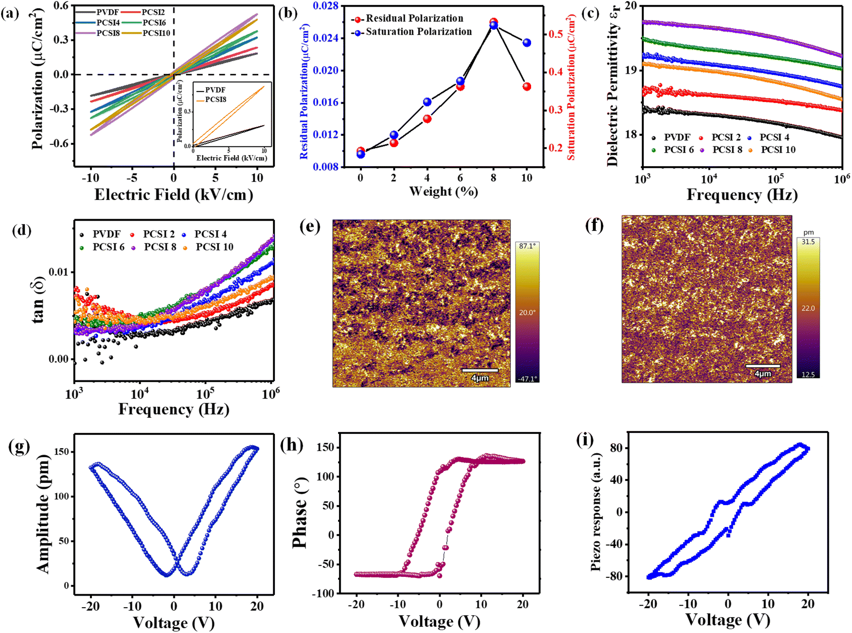 | ||
| Fig. 4 (a) P–E loop of PVDF and PCSIs and the inset shows the zoomed PE loop of PVDF and PCSI8, (b) residual and saturation polarization as a function of weight%, (c) variation of εr with frequency, (d) dielectric loss of the composites as a function of frequency, (e) the amplitude image, (f) the phase image, (g) the amplitude vs. bias, (h) the phase vs. bias, and (i) piezo response vs. bias loops. | ||
Impedance spectroscopy (IS) is a useful study that explores the electrical properties of a material as a function of frequency and temperature. It helps in understanding the behavior of bound and mobile charges, energy storage, and dissipation in solid-state devices. The temperature-dependent complex dielectric permittivity spectra were deduced using the IS data. A qualitative discussion on the complex impedance spectra, comprising frequency and temperature variation in the real (Z′(ω)) and imaginary (Z′′(ω)) parts of impedance, can also be found in the ESI.†
The behavior of a dielectric material towards an electric field can be understood using complex dielectric formalism, which is represented as
| ε*(ω) = ε′(ω) − jε′′(ω) |

where

 is the free space capacitance, εo is the permittivity of free space, A is the area of the electrode, and d is the thickness of the pellet.
Fig. S10(c) and (d)† show the frequency dependent ε′(ω) and ε′′(ω), respectively, at different temperatures, indicating that ε′(ω) and ε′′(ω) are higher when the frequency is low and gradually decreases when the frequency increases for a particular temperature. The dielectric behavior mainly depends on electronic, ionic, interfacial, and orientational polarizations. ε′(ω) is higher in the low frequency region and decreases as the frequency increases. In the low frequency region (<10 kHz), interfacial polarizations are more dominant, which contributes to the value of the dielectric constant, ε′(ω). However, in the high frequency region (>10 kHz), orientational, electronic, and ionic polarizations take over. At low frequencies, dipoles in the material have enough time to align themselves with the applied field, leading to a high dielectric constant. Since the orientation polarization also depends on the temperature, ε′(ω) also increases with the increase in temperature. However, the dipoles struggle to keep up with the fast-changing field, hence the reduced dielectric constant. To understand whether or not the materials (Cs3Sb2I9, PVDF, and PCSI) exhibit ferroelectric phase transition, we further checked the ε′ vs. T behavior at higher frequencies (>10 kHz), as shown in Fig. S10(e)–(g).† However, in the ε′ vs. T plot, we do not observe the typical λ-shaped behavior characteristic of a ferro-to-paraelectric phase transition, which indicates the predominant dielectric nature of Cs3Sb2I9 and the composite samples. The ε′ value for PCSI8 shows a strong temperature dependence as compared to that for Cs3Sb2I9 and bare PVDF, implying that PCSI8 has a higher tendency to orient dipoles compared to Cs3Sb2I9 and bare PVDF. However, none of the samples follow the typical Curie–Wiess law for the ferroelectric to paraelectric transition.
The dielectric loss, ε′′(ω), shows higher values at low frequencies but decreases when the frequency increases. At low frequencies, the charge carriers experience higher resistance due to space charge accumulation at the grain boundaries, which leads to more energy dissipation. However, at higher frequencies, charge carriers cannot follow the fast switching of the field, and hence, the conduction loss is reduced significantly, which is consistent with Koop's phenomenological theory.64 We also plotted the loss tangent, tanδ, as a function of frequency at various temperatures, as shown in Fig. S10(h).† It is the ratio of dielectric loss to dielectric constant (ε′′/ε′) which provides the energy dissipation caused by charge carrier conduction represented by broad loss peaks. The occurrence of this peak is because of the alignment of the hopping frequency with the frequency of the applied external field. The loss peaks also shift to higher frequencies as temperature increases because of temperature-activated hopping phenomena.
The dielectric properties of the composites are significant for energy storage devices. A material's dielectric constant can reveal its charging capacity, while the dielectric loss feature accounts for the energy dissipation in every cycle. The dielectric nature of PCSIs is similarly affected by the addition of Cs3Sb2I9 to PVDF. Fig. 4(c) shows the dielectric permittivity (εr) of all the PCSIs in the frequency range of 1 kHz to 1 MHz at ambient temperature. The εr values of all the composites are greater than that of pure PVDF. As the loading amount of Cs3Sb2I9 is increased, the value of εr also increases, which may be attributed to the interfacial interaction between PVDF and some preferred terminations of Cs3Sb2I9 surfaces.52 Among all the composites, PCSI8 has the highest εr value, and beyond 8% loading of the perovskite in the PVDF matrix, it decreases because of agglomeration. The larger values of εr at a low-frequency range are a cumulative effect of the ionic, interfacial, dipolar, and electronic polarizations. However, the value of εr decreases as the frequency increases, owing to the weakening of interfacial/space polarization.65Fig. 4(d) shows the dielectric loss (tan(δ)) of the composites as a function of frequency. The dielectric loss of the composites increases rapidly after the frequency of 10 kHz because of the relaxation loss. The stored energy density and the energy loss density were calculated by integrating the different parts of the P–E loop (Fig. 4(a)) using the following formula:6,62
| U = ∫EdP | (2) |
The piezoresponse force microscopy (PFM) analysis was performed to check the piezo-response of the composite film PCSI8. The amplitude and phase images over an area of 25 μm × 25 μm are shown in Fig. 4(e) and (f), respectively. In Fig. 4(g), the composite shows an amplitude “butterfly” loop with a maximum deformation of ∼150 pm under ±20 V bias (OFF state). Fig. 4(h) shows the phase response loop of the PCSI8 composite with ±20 V applied bias voltage. The OFF state is preferred for these experiments to reduce the effects of electrostatic interactions. The piezoelectric coefficient (d33) calculated using the formula Adeflection = d33Eac is ∼7.48 pm V−1, which is higher than that of other materials such as GaN (3.1 pm V−1), NaNbO3 (4 pm V−1), and MAPbI3.66–68 The mechanical strain developed within the film under an applied field affirms the presence of piezo-response in the composite. The piezo-response hysteresis loop is shown in Fig. 4(i), obtained by Pr = A(E)cos[ϕ(E)], where A(E) and ϕ(E) are the amplitude and phase as a function of the applied electric field, respectively.49 The 3D topographical image is shown in Fig. S12 (see the ESI).†
4.2 Piezoelectric nanogenerator performance for energy harvesting application
To investigate the piezoelectric response for energy harvesting applications, the nanogenerator devices of bare PVDF and PCSIs were fabricated. The schematic of the device configuration is shown in Fig. S13 (see the ESI).† The effective area of the device is 7 × 2 cm2 and the piezoelectric effect was obtained by repeated hand hammering without any external electric poling. We recorded the open circuit voltage and the short circuit current of all the devices, as shown in Fig. 5(a) and (b), respectively. The open circuit voltage (Fig. 5(a)) and the short circuit current (Fig. 5(b)) of PVDF are ∼17 V and 0.5 μA, which increased up to ∼85 V and ∼2.6 μA for PCSI8 because of the highest content of the electroactive phase (∼82%) in the composite. Although the output performances for all the PCSIs are better than bare PVDF, the PCSI8 device showed the best performance. The dependence of output voltage and current as a function of load resistance was also studied. The resistance was connected in series with PCSI8 and varied from 1 kΩ to 10 MΩ. In Fig. 5(c), the output voltage gets saturated at high resistance values while the current follows the reverse trend of the output voltage. The variation of the output power of PCSI8 as a function of the load resistance is shown in Fig. 5(d), yielding a maximum output power density of ∼1.26 μW cm−2 across a 0.8 MΩ resistor. The power density of PVDF as a function of resistance is shown in Fig. S14 (see the ESI).† For PCSI8, the best-performing device, with the addition of 8% Cs3Sb2I9 in PVDF, the voltage increases by 80% and power density increases ∼320 times that of pure PVDF. Upon changing the polarity of PCSI8, the output voltages in the forward and reverse bias connections are almost the same (Fig. 5(e)), confirming that the voltage is primarily due to a piezoelectric effect. Fig. 5(f) shows the DC output voltage of PCSI8, obtained using a bridge rectifier circuit. A schematic in Fig. 5(g) explains the mechanism of the generation of piezoelectric potential from PCSIs under mechanical stress. The molecular dipoles are represented by strips having positive and negative charges at the ends. The polarization is defined as the sum of the electric dipole moment of all the molecular dipoles per unit volume. The molecular dipoles have different dipole moments. Initially, when there is no force imparted on the composites, they are oriented randomly, making the total electric dipole moment of the system zero, and hence, there is no electric signal in the external circuit. When a mechanical force is applied to the top surface of the PCSI, the electric dipoles get oriented in the direction of the applied force. So, the electric dipole moment occurs in the composite, and positive and negative charges are induced at the top and bottom surfaces. The applied pressure deforms the crystalline structure, which has weaker van der Waals contact and electrostatic interaction, generating a piezoelectric potential between the two surfaces. This piezoelectric potential causes charges on the top and bottom electrodes, generating a positive voltage signal. Conversely, when the pressure is released, the piezoelectric potential vanishes, and the stored electrons flow in the opposite direction, resulting in a negative or reverse voltage signal.62,69,70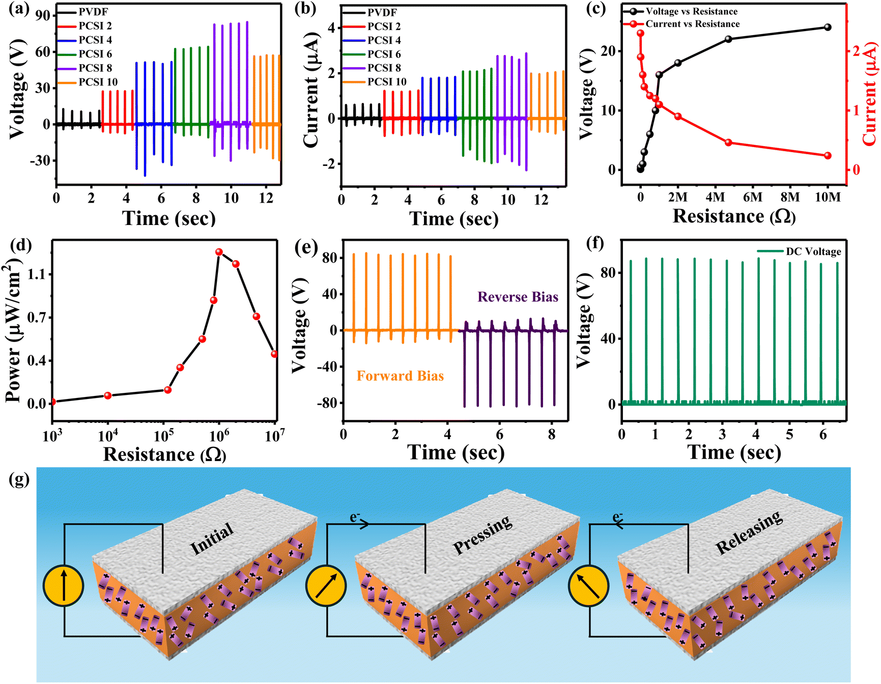 | ||
| Fig. 5 (a) The open circuit voltage and (b) short circuit current of all the devices. (c) Voltage and current as a function of load resistance, (d) power density vs. resistance, (e) voltage response in forward and reverse bias configuration, (f) rectified DC voltage of the PCSI8 device, and (g) schematic representation of the working mechanism of the piezoelectric response under external mechanical deformation. | ||
Fig. S15 (see the ESI†) illustrates the output voltage of PCSI8 under varying conditions of frequency and applied force. Fig. S15(a)† shows that the output voltage remains relatively consistent with different frequencies (0.5 Hz to 10 Hz). However, the number of voltage cycles increases with frequency. In Fig. S15(b),† the output voltage is shown under varying applied forces, where an increase in the force from 1 N to 9 N leads to a significant rise in voltage, suggesting that the nanogenerator is responsive to applied force variations.
To show the energy harvesting capability of PCSI8 via physiological motions, we performed various human motions and observed the output voltages due to them. The output voltages corresponding to finger bending (∼0.9 V), elbow bending (∼0.7 V), knee bending (∼0.8 V), heel pressing (∼2.1 V), and toe pressing (∼5.2 V) were recorded and are shown in Fig. 6(a)–(e). Fig. 6(f) shows the charging of capacitors of values 2.2 μF, 4.7 μF, 10 μF, 33 μF, 47 μF, and 470 μF using the PCSI8 device via a bridge rectifier circuit, shown in Fig. 6(g). The charging voltage increases exponentially and gets saturated at 2.2 V. The capacitor with a lower value of capacitance gets charged much earlier. The ability to charge different capacitors in a reasonably quick time indicates that the PCSIs can be used as energy storage devices to self-power portable electronic gadgets. The device's longevity, durability, and reproducible output response are checked using a long-cycle fatigue test. The output voltage of PSCI8, shown in Fig. 6(h), remains constant during the long-cycle operation for 10000 continuous cycles. The comparison of other reported nanogenerators' performance is shown in Table S1 (see the ESI).† Using only hand-hammering motion, the PCSI8 device also successfully illuminated an array of commercially available LEDs, as shown in Fig. 6(i); the video of which is available as a video in the ESI (VS1).†
 | ||
| Fig. 6 The output voltage of PCSI8 due to (a) finger bending, (b) elbow bending, (c) knee bending, (d) heel pressing, (e) toe pressing, and (f) capacitor charging, (g) the circuit for capacitor charging, (h) long cycle output voltage up to 10000 cycles, and (i) glowing LEDs. | ||
4.3 DFT study
In order to validate the experimental results, DFT calculations were performed. We considered the orthorhombic β-phase of PVDF as shown in Fig. S16(a) (see the ESI).† The Cs3Sb2l9 crystal structure is shown in Fig. S16(b) (see the ESI).† Based on the XRD data, we selected the most prominent peaks associated with the (203) plane of Cs3Sb2I9 to establish the composite with a long chain of polyvinylidene fluoride (PVDF). After optimizing the long chains of the PVDF polymer on the surface of Cs3Sb2I9 (203), we observed that PVDF forms bonds by physisorption. The optimized structure of Cs3Sb2I9–PVDF is shown in Fig. S16(c) (see the ESI).†To understand the electronic properties, we have estimated the Density of States (DOS) for Cs3Sb2I9, PVDF, and Cs3Sb2I9–PVDF systems. The DOS results of Cs3Sb2I9, PVDF and Cs3Sb2I9–PVDF systems are depicted in Fig. 7(a), (b), and (c), respectively.53,69 It is noticeable from Fig. 7(a)–(c) that there is a symmetric behavior of the density of states for up and down spins, demonstrating the non-magnetic properties of these compounds. Furthermore, there is a distinct separation between valence band maxima (VBM) and conduction band minima (CBM), which represents the insulating behavior of these compounds. Fig. 7(a)–(c) clearly shows that there is a reduction in the band gap (Eg) while the Cs3Sb2I9 surfaces interact with PVDF. The reduction in the band gap occurs due to the shift of p-orbital conduction states towards lower energy of antimony and iodine, respectively, which is shown in Fig. 7(d) and (e). The cause of this shift can be attributed to the interaction between Cs3Sb2I9 and PVDF layers.71 Work function calculations were carried out to determine how easily an electron can be removed from these materials to an external environment. Work functions for Cs3Sb2I9, PVDF, and Cs3Sb2I9–PVDF are depicted in Fig. 7(f)–(h). In our calculation, the work functions for Cs3Sb2I9 and PVDF are determined to be 4.74 eV and 6.46 eV, respectively. For the composite material Cs3Sb2I9–PVDF, the work function is measured at 5.27 eV. Once the composite is formed, the material exhibits a reduced work function. This suggests that electrons can readily transition from the Fermi level to the external environment, indicating the favorable electron emission characteristics of the composite material.
 | ||
| Fig. 7 (a), (b) and (c) represent the total DOS of Cs3Sb2I9, PVDF and Cs3Sb2I9–PVDF, respectively; (d) and (e) show the PDOS of Sb-p and I-p orbitals, respectively in the Cs3Sb2I9–PVDF composite; (f), (g) and (h) show the work function of Cs3Sb2I9, PVDF and Cs3Sb2I9–PVDF structures. | ||
4.4 Piezo-phototronic effect
We further demonstrated the piezo-phototronic effect in the PCSI8 of Cs3Sb2I9 and PVDF under positive and negative strain in the presence of light. The device was prepared by placing PCSI8 on a flexible substrate. Then, the silver contact for the photodetection was made using a physical vapor deposition technique, and two wires were connected at the ends with silver paste with an active area of 2.5 × 1.6 cm2. Fig. 8(a) shows the schematic of the customized setup for investigating the piezo-phototronic effect, where the orange-colored film with two electrodes between the two blue boxes is PCSI8. Here, one end was kept fixed while the other could be moved to bend the film in different curvatures, creating both positive and negative strain in the composite. | ||
| Fig. 8 (a) Schematic diagram for the measurement of the piezo-phototronic effect, (b) I–V measurement of PCSI8 under positive and negative strain and under illuminated conditions, (c) I–V measurement of PCSI8 under positive and negative strain and under dark conditions, (d) change in the current of the photodetector under dark and illuminated conditions, and schematic structure and energy band diagrams of PCSI8: (e) without strain and under dark conditions, (f) with strain and under dark conditions, and (h) with strain and under illuminated conditions. | ||
The bending strain was calculated as:
 | (3) |
The bending radius was calculated using:
 | (4) |
The derivation of eqn (4) is provided in the ESI text.† Here, L and L − L0 are the initial and reduced lengths, respectively.
The current–voltage data were recorded under a bias of ±10 V, and the strain was varied from −1.37% to +1.37% under irradiated conditions. In Fig. 8(b), the photocurrent increases with an increment in positive strain under light illumination, which can be ascribed to the piezo-phototronic effect in the PCSI composite.13,47,72–75 When the positive strain is applied, a positive piezoelectric potential is generated, which decreases the Schottky barrier height (SBH), facilitating the transportation of the electrons. This reduction of the barrier height aids the electron–hole separation and decreases the recombination of the electron–hole pairs, ultimately increasing the photocurrent. However, when the negative strain is applied to the composite, the photocurrent is reduced with the increment in the negative strain. This is because the negative strain induces the negative piezoelectric potential, leading to an increment in the Schottky barrier height, which opposes the transportation of the electron and, consequently, less photocurrent is generated.47,73 Furthermore, when the positive and negative strains were applied to the PCSI in the dark, the effect of piezoelectric potential on the dark current in both cases was negligible,73 as shown in Fig. 8(c).
We also measured the short-circuit current under dark and illuminated conditions on a photodetection-based device, similar to a piezoelectric nanogenerator. The self-powered photodetector was fabricated by depositing the solution of PCSI8 on a flexible ITO-coated PET substrate and applying a top contact. Under dark conditions, Isc was approximately 0.47 μA, and under light irradiation, it was ∼1.3 μA, leading to the enhancement in Isc by 63%, as shown in Fig. 8(d). To understand the mechanism, a schematic of the energy band diagram is shown in Fig. 8(e) and (f). In the Cu/PCSI/ITO architecture, the interface between Cu and PCSI is metal-semiconductor contact, while that between PCSI and ITO is an ohmic contact. The schematic of the device with the energy band diagram is shown in Fig. 8(e) under unstrained and light-off conditions. When a compressive strain was applied to PCSI, the positive and negative charges merged at the surface of PCSI due to the piezoelectric potential. Due to this, a change in the Schottky barrier height occurs, which determines the flow of the charge carriers through the contact. As discussed earlier, the positive and negative piezoelectric potentials will cause a change in the SBH. So, the energy band at the Cu/PCSI contact goes down, and the energy band at the PCSI/ITO contact goes up, as demonstrated in Fig. 8(f).76 When the light is irradiated on it, the charge carriers will be generated in the PCSI, and the piezoelectric potential due to strain helps in the separation of electron–hole pairs, preventing their recombination process and increasing the current density, as shown in Fig. 8(g). We also measured the output voltage under dark and irradiated conditions. Under dark conditions, it was ∼8.6 V, and when the light was turned on, the output voltage decreased to ∼6.2 V, a drop of ∼28%, as shown in Fig. S18 (see the ESI).† When the light is on, the photo-generated charge carriers start moving within PCSI, generating a local electromagnetic field that can prevent the movement of the charge carriers, as shown in Fig. 8(g). Due to this, there will be less flow of free electrons in the circuit, resulting in less output voltage. Thus, we successfully demonstrate the piezo-phototronic effect in PCSI, which can be used as a self-powered optoelectronic device. These composites have tremendous potential to be employed as optoelectronic sensors due to their synergistic properties encompassing enhanced biomechanical energy harvesting as well as photodetection properties.
5. Conclusion
In conclusion, we have successfully developed an environment-friendly, easily processable, cost-effective, flexible, mechanically robust, and self-sustaining device based on a lead-free halide perovskite (Cs3Sb2I9) and PVDF composite. Controlled incorporation of Cs3Sb2I9 into the PVDF matrix could enhance the nucleation of the electroactive (β) phase content. The best device (obtained by loading 8% of Cs3Sb2I9 into the PVDF matrix) exhibited appreciable performance with approximately ∼82% of β phase activation and a piezoelectric coefficient of ∼7.48 pm V−1, which is significantly higher than bare PVDF. The dielectric permittivity of the composites also increased with the addition of Cs3Sb2I9 into PVDF, making them suitable for energy storage devices. The device displayed a maximum remanent polarization of 0.026 μC cm−2 and a saturation polarization of 0.525 μC cm−2). Furthermore, the device generated a maximum open circuit voltage of ∼85 V, a short circuit current of ∼2.6 μA and a maximum power density of ∼1.26 μW cm−2 (across a 0.8 MΩ resistor), which can sustain portable electronic gadgets and exhibited impressive durability and repeatability, withstanding up to 10000 cycles. DFT calculation was carried out to understand the interactions of the perovskite surfaces with PVDF. It is noted from the calculations that the composite exhibited a reduced work function (5.27 eV), indicating favorable electron emission characteristics. Finally, we realized the piezo-phototronic effect in the composite by combining the piezoresponse and photoexcitation processes, yielding a photocurrent increment of 63%, with prospective applications in integrated piezotronic sensing and optoelectronic devices.
Data availability
The data supporting this article have been included as part of the ESI.†Author contributions
Prabhat Kumar: investigation; conceptualization; formal analysis; writing – original draft. Tufan Paul: conceptualization; validation; visualization. Aditi Sahoo: investigation; validation. Manoj Singh: conceptualization; data curation; methodology. Arupjyoti Pathak: data curation; methodology. Ranjit Thapa: software; supervision; validation; writing – review & editing. Rupak Banerjee: investigation; funding acquisition; resources; supervision; validation; writing – review & editing.Conflicts of interest
There are no conflicts to declare.Acknowledgements
Funding from the MoE-STARS, Govt. of India, under the project MoE-STARS/STARS-1/231 and ANRF, Govt. of India, under the project CRG/2022/005258 is gratefully acknowledged. We also thank the Central Instrumentation Facility at IIT Gandhinagar for facilitating several measurements. RT thanks Science and Engineering Research Board (SERB), India, for financial support (Grant No. CRG/2022/005423) and the SRM University-AP, Andhra Pradesh, for providing the central computational facilities.References
- I.-Y. Suh, Y.-J. Kim, P. Zhao, D. S. Cho, M. Kang, Z.-Y. Huo and S.-W. Kim, Self-powered microbial blocking textile driven by triboelectric charges, Nano Energy, 2023, 110, 108343, DOI:10.1016/j.nanoen.2023.108343.
- S. J. Kim, J. H. We and B. J. Cho, A wearable thermoelectric generator fabricated on a glass fabric, Energy Environ. Sci., 2014, 7, 1959–1965, 10.1039/C4EE00242C.
- N. H. Makani, A. Sahoo, P. Pal, T. Paul, L. S. Tanwar, M. Singh, A. Ghosh and R. Banerjee, Onset of vacancy-mediated high activation energy leads to large ionic conductivity in two-dimensional layered Cs2PbI2Cl2 Ruddlesden-Popper halide perovskite, Phys. Rev. Mater., 2022, 6, 115002, DOI:10.1103/PhysRevMaterials.6.115002.
- R. J. Sutton, G. E. Eperon, L. Miranda, E. S. Parrott, B. A. Kamino, J. B. Patel, M. T. Hörantner, M. B. Johnston, A. A. Haghighirad, D. T. Moore and H. J. Snaith, Bandgap-Tunable Cesium Lead Halide Perovskites with High Thermal Stability for Efficient Solar Cells, Adv. Energy Mater., 2016, 6, 1502458, DOI:10.1002/aenm.201502458.
- M. T. Khan, M. Salado, A. Almohammedi, S. Kazim and S. Ahmad, Elucidating the Impact of Charge Selective Contact in Halide Perovskite through Impedance Spectroscopy, Adv. Mater. Interfaces, 2019, 6, 1901193, DOI:10.1002/admi.201901193.
- N. H. Makani, P. Kumar, T. Paul, A. Sahoo, S. Maiti and R. Banerjee, Low-dimensional halide perovskite/PVDF nanocomposite with enhanced piezoelectricity as flexible biomechanical energy harvester, Chem. Phys. Impact, 2024, 8, 100564, DOI:10.1016/j.chphi.2024.100564.
- M. Singh, J. Nama, T. Paul, N. H. Makani, A. Sahoo, S. Sharma and R. Banerjee, Photoelectrochemically Induced CO2 Reduction Using Halide-Tunable Lead-Free Perovskites, ACS Appl. Energy Mater., 2023, 6, 3566–3578, DOI:10.1021/acsaem.3c00053.
- J. Xu, W. Huang, P. Li, D. R. Onken, C. Dun, Y. Guo, K. B. Ucer, C. Lu, H. Wang, S. M. Geyer, R. T. Williams and D. L. Carroll, Imbedded Nanocrystals of CsPbBr3 in Cs4PbBr6 : Kinetics, Enhanced Oscillator Strength, and Application in Light-Emitting Diodes, Adv. Mater., 2017, 29, 1703703, DOI:10.1002/adma.201703703.
- M. R. Leyden, L. K. Ono, S. R. Raga, Y. Kato, S. Wang and Y. Qi, High performance perovskite solar cells by hybrid chemical vapor deposition, J. Mater. Chem. A, 2014, 2, 18742–18745, 10.1039/C4TA04385E.
- A. Sahoo, T. Paul, P. Pal, N. H. Makani, A. Ghosh and R. Banerjee, Dielectric Relaxation Mechanism in the Phase-Transition Region of a Chiral Hybrid Perovskite and Its Piezoelectric-Energy-Harvesting Properties, Phys. Rev. Appl., 2023, 20, 034024, DOI:10.1103/PhysRevApplied.20.034024.
- J. Kwon, W. Seung, B. K. Sharma, S.-W. Kim and J.-H. Ahn, A high performance PZT ribbon-based nanogenerator using graphene transparent electrodes, Energy Environ. Sci., 2012, 5, 8970–8975, 10.1039/C2EE22251E.
- Z. L. Wang, Triboelectric Nanogenerators as New Energy Technology for Self-Powered Systems and as Active Mechanical and Chemical Sensors, ACS Nano, 2013, 7, 9533–9557, DOI:10.1021/nn404614z.
- Q. Lai, L. Zhu, Y. Pang, L. Xu, J. Chen, Z. Ren, J. Luo, L. Wang, L. Chen, K. Han, P. Lin, D. Li, S. Lin, B. Chen, C. Pan and Z. L. Wang, Piezo-phototronic Effect Enhanced Photodetector Based on CH3NH3PbI3 Single Crystals, ACS Nano, 2018, 12, 10501–10508, DOI:10.1021/acsnano.8b06243.
- X. Chen, X. Li, J. Shao, N. An, H. Tian, C. Wang, T. Han, L. Wang and B. Lu, High-Performance Piezoelectric Nanogenerators with Imprinted P(VDF-TrFE)/BaTiO3 Nanocomposite Micropillars for Self-Powered Flexible Sensors, Small, 2017, 13, 1604245, DOI:10.1002/smll.201604245.
- S. Barsiwal, A. Babu, U. K. Khanapuram, S. Potu, N. Madathil, R. K. Rajaboina, S. Mishra, H. Divi, P. Kodali, R. Nagapuri and T. Chinthakuntla, ZIF-67-Metal–Organic-Framework-Based Triboelectric Nanogenerator for Self-Powered Devices, Nanoenergy Adv., 2022, 2, 291–302, DOI:10.3390/nanoenergyadv2040015.
- Q. Zheng, M. Peng, Z. Liu, S. Li, R. Han, H. Ouyang, Y. Fan, C. Pan, W. Hu, J. Zhai, Z. Li and Z. L. Wang, Dynamic real-time imaging of living cell traction force by piezo-phototronic light nano-antenna array, Sci. Adv., 2021, 7, eabe7738, DOI:10.1126/sciadv.abe7738.
- X. Gong, M. Tong, Y. Xia, W. Cai, J. S. Moon, Y. Cao, G. Yu, C.-L. Shieh, B. Nilsson and A. J. Heeger, High-Detectivity Polymer Photodetectors with Spectral Response from 300 nm to 1450 nm, Science, 2009, 325, 1665–1667, DOI:10.1126/science.1176706.
- A. Swarnkar, A. R. Marshall, E. M. Sanehira, B. D. Chernomordik, D. T. Moore, J. A. Christians, T. Chakrabarti and J. M. Luther, Quantum dot-induced phase stabilization of α-CsPbI3 perovskite for high-efficiency photovoltaics, Science, 2016, 354, 92–95, DOI:10.1126/science.aag2700.
- S. Mondal, T. Paul, S. Maiti, B. K. Das and K. K. Chattopadhyay, Human motion interactive mechanical energy harvester based on all inorganic perovskite-PVDF, Nano Energy, 2020, 74, 104870, DOI:10.1016/j.nanoen.2020.104870.
- A. Sultana, P. Sadhukhan, M. Alam, S. Das, T. Middya and D. Mandal, Organo-Lead Halide Perovskite Induced Electroactive β-Phase in Porous PVDF Films: An Excellent Material for Photoactive Piezoelectric Energy Harvester and Photodetector, ACS Appl. Mater. Interfaces, 2018, 10, 4121–4130, DOI:10.1021/acsami.7b17408.
- D. B. Kim, K. S. Jo, K. S. Park and Y. S. Cho, Anion-Dependent Polarization and Piezoelectric Power Generation in Hybrid Halide MAPbX3 (X = I, Br, and Cl) Thin Films with Out-of-Plane Structural Adjustments (Adv. Sci. 4/2023), Adv. Sci., 2023, 10, 2370022, DOI:10.1002/advs.202370022.
- D. B. Kim, K. H. Park and Y. S. Cho, Origin of high piezoelectricity of inorganic halide perovskite thin films and their electromechanical energy-harvesting and physiological current-sensing characteristics, Energy Environ. Sci., 2020, 13, 2077–2086, 10.1039/C9EE03212F.
- W. Liao, D. Zhao, Y. Yu, C. R. Grice, C. Wang, A. J. Cimaroli, P. Schulz, W. Meng, K. Zhu, R.-G. Xiong and Y. Yan, Lead-Free Inverted Planar Formamidinium Tin Triiodide Perovskite Solar Cells Achieving Power Conversion Efficiencies up to 6.22, Adv. Mater., 2016, 28, 9333–9340, DOI:10.1002/adma.201602992.
- J. Zillner, H.-G. Boyen, P. Schulz, J. Hanisch, N. Gauquelin, J. Verbeeck, J. Küffner, D. Desta, L. Eisele, E. Ahlswede and M. Powalla, The Role of SnF2 Additive on Interface Formation in All Lead-Free FASnI3 Perovskite Solar Cells, Adv. Funct. Mater., 2022, 32, 2109649, DOI:10.1002/adfm.202109649.
- R. Chiara, M. Morana and L. Malavasi, Germanium-Based Halide Perovskites: Materials, Properties, and Applications, ChemPlusChem, 2021, 86, 879–888, DOI:10.1002/cplu.202100191.
- Y. Raoui, S. Kazim, Y. Galagan, H. Ez-Zahraouy and S. Ahmad, Harnessing the potential of lead-free Sn–Ge based perovskite solar cells by unlocking the recombination channels, Sustainable Energy Fuels, 2021, 5, 4661–4667, 10.1039/D1SE00687H.
- P. Chandra, S. Saha and S. K. Mandal, A dielectric study of Br-doped lead-free methylammonium bismuth chloride (CH3NH3)3Bi2BrxCl9−x, Appl. Phys. A, 2022, 128, 541, DOI:10.1007/s00339-022-05677-9.
- H. Lei, D. Hardy and F. Gao, Lead-Free Double Perovskite Cs2AgBiBr6: Fundamentals, Applications, and Perspectives, Adv. Funct. Mater., 2021, 31, 2105898, DOI:10.1002/adfm.202105898.
- J. Deng, L. Yang, X. Zhang, K. Wei, G. Du, G. Zhu and J. Zhang, Synergistic effects of morphological control and enhanced charge collection enable efficient and stable lead-free CsBi3I10 thin film solar cells, J. Mater. Chem. A, 2022, 10, 9384–9392, 10.1039/D1TA10808E.
- Y. Yang, C. Liu, M. Cai, Y. Liao, Y. Ding, S. Ma, X. Liu, M. Guli, S. Dai and M. K. Nazeeruddin, Dimension-Controlled Growth of Antimony-Based Perovskite-like Halides for Lead-Free and Semitransparent Photovoltaics, ACS Appl. Mater. Interfaces, 2020, 12, 17062–17069, DOI:10.1021/acsami.0c00681.
- W. Guo, Y. Zhu, M. Zhang, J. Du, Y. Cen, S. Liu, Y. He, H. Zhong, X. Wang and J. Shi, The Dion–Jacobson perovskite CsSbCl4: a promising Pb-free solar-cell absorber with optimal bandgap ∼1.4 eV, strong optical absorption ∼105 cm−1, and large power-conversion efficiency above 20%, J. Mater. Chem. A, 2021, 9, 16436–16446, 10.1039/D1TA02969J.
- Z.-H. Lin, Y. Yang, J. M. Wu, Y. Liu, F. Zhang and Z. L. Wang, BaTiO3 Nanotubes-Based Flexible and Transparent Nanogenerators, J. Phys. Chem. Lett., 2012, 3, 3599–3604, DOI:10.1021/jz301805f.
- S. Xu, B. J. Hansen and Z. L. Wang, Piezoelectric-nanowire-enabled power source for driving wireless microelectronics, Nat. Commun., 2010, 1, 93, DOI:10.1038/ncomms1098.
- F. Wu, W. Cai, Y.-W. Yeh, S. Xu and N. Yao, Energy scavenging based on a single-crystal PMN-PT nanobelt, Sci. Rep., 2016, 6, 22513, DOI:10.1038/srep22513.
- J. H. Jung, M. Lee, J.-I. Hong, Y. Ding, C.-Y. Chen, L.-J. Chou and Z. L. Wang, Lead-Free NaNbO3 Nanowires for a High Output Piezoelectric Nanogenerator, ACS Nano, 2011, 5, 10041–10046, DOI:10.1021/nn2039033.
- K. Y. Lee, D. Kim, J. Lee, T. Y. Kim, M. K. Gupta and S. Kim, Unidirectional High-Power Generation via Stress-Induced Dipole Alignment from ZnSnO3 Nanocubes/Polymer Hybrid Piezoelectric Nanogenerator, Adv. Funct. Mater., 2014, 24, 37–43, DOI:10.1002/adfm.201301379.
- Y. Hu, C. Xu, Y. Zhang, L. Lin, R. L. Snyder and Z. L. Wang, A Nanogenerator for Energy Harvesting from a Rotating Tire and its Application as a Self-Powered Pressure/Speed Sensor, Adv. Mater., 2011, 23, 4068–4071, DOI:10.1002/adma.201102067.
- Y.-F. Lin, J. Song, Y. Ding, S.-Y. Lu and Z. L. Wang, Piezoelectric nanogenerator using CdS nanowires, Appl. Phys. Lett., 2008, 92, 022105, DOI:10.1063/1.2831901.
- J. M. Wu and C. C. Kao, Self-powered pendulum and micro-force active sensors based on a ZnS nanogenerator, RSC Adv., 2014, 4, 13882–13887, 10.1039/C3RA47435F.
- L. Lin, C.-H. Lai, Y. Hu, Y. Zhang, X. Wang, C. Xu, R. L. Snyder, L.-J. Chen and Z. L. Wang, High output nanogenerator based on assembly of GaN nanowires, Nanotechnology, 2011, 22, 475401, DOI:10.1088/0957-4484/22/47/475401.
- S. Mohammadpourfazeli, S. Arash, A. Ansari, S. Yang, K. Mallick and R. Bagherzadeh, Future prospects and recent developments of polyvinylidene fluoride (PVDF) piezoelectric polymer; fabrication methods, structure, and electro-mechanical properties, RSC Adv., 2023, 13, 370–387, 10.1039/D2RA06774A.
- X. Cai, T. Lei, D. Sun and L. Lin, A critical analysis of the α, β and γ phases in poly(vinylidene fluoride) using FTIR, RSC Adv., 2017, 7, 15382–15389, 10.1039/c7ra01267e.
- N. Soin, P. Zhao, K. Prashanthi, J. Chen, P. Ding, E. Zhou, T. Shah, S. C. Ray, C. Tsonos, T. Thundat, E. Siores and J. Luo, High performance triboelectric nanogenerators based on phase-inversion piezoelectric membranes of poly(vinylidene fluoride)-zinc stannate (PVDF-ZnSnO3) and polyamide-6 (PA6), Nano Energy, 2016, 30, 470–480, DOI:10.1016/j.nanoen.2016.10.040.
- D. Mandal, K. Henkel and D. Schmeißer, Improved performance of a polymer nanogenerator based on silver nanoparticles doped electrospun P(VDF–HFP) nanofibers, Phys. Chem. Chem. Phys., 2014, 16, 10403–10407, 10.1039/C3CP55238A.
- A. Sultana, Md. M. Alam, P. Sadhukhan, U. K. Ghorai, S. Das, T. R. Middya and D. Mandal, Organo-lead halide perovskite regulated green light emitting poly(vinylidene fluoride) electrospun nanofiber mat and its potential utility for ambient mechanical energy harvesting application, Nano Energy, 2018, 49, 380–392, DOI:10.1016/j.nanoen.2018.04.057.
- N. Meng, X. Ren, G. Santagiuliana, L. Ventura, H. Zhang, J. Wu, H. Yan, M. J. Reece and E. Bilotti, Ultrahigh β-phase content poly(vinylidene fluoride) with relaxor-like ferroelectricity for high energy density capacitors, Nat. Commun., 2019, 10, 4535, DOI:10.1038/s41467-019-12391-3.
- J. Sun, Q. Hua, R. Zhou, D. Li, W. Guo, X. Li, G. Hu, C. Shan, Q. Meng, L. Dong, C. Pan and Z. L. Wang, Piezo-phototronic Effect Enhanced Efficient Flexible Perovskite Solar Cells, ACS Nano, 2019, 13, 4507–4513, DOI:10.1021/acsnano.9b00125.
- J. Nie, Y. Zhang, L. Li and J. Wang, Piezo-phototronic effect enhanced photodetectors based on MAPbI3 perovskite, J. Mater. Chem. C, 2020, 8, 2709–2718, 10.1039/C9TC05721H.
- A. Sahoo, T. Paul, N. Hiralal Makani, S. Maiti and R. Banerjee, High piezoresponse in low-dimensional inorganic halide perovskite for mechanical energy harvesting, Sustainable Energy Fuels, 2022, 6, 4484–4497, 10.1039/D2SE00786J.
- G. Kresse and D. Joubert, From ultrasoft pseudopotentials to the projector augmented-wave method, Phys. Rev. B:Condens. Matter Mater. Phys., 1999, 59, 1758–1775, DOI:10.1103/PhysRevB.59.1758.
- P. E. Blöchl, Projector augmented-wave method, Phys. Rev. B:Condens. Matter Mater. Phys., 1994, 50, 17953–17979, DOI:10.1103/PhysRevB.50.17953.
- J. P. Perdew, K. Burke and M. Ernzerhof, Generalized Gradient Approximation Made Simple, Phys. Rev. Lett., 1996, 77, 3865–3868, DOI:10.1103/PhysRevLett.77.3865.
- B. Saparov, F. Hong, J.-P. Sun, H.-S. Duan, W. Meng, S. Cameron, I. G. Hill, Y. Yan and D. B. Mitzi, Thin-Film Preparation and Characterization of Cs3Sb2I9: A Lead-Free Layered Perovskite Semiconductor, Chem. Mater., 2015, 27, 5622–5632, DOI:10.1021/acs.chemmater.5b01989.
- S. Grimme, J. Antony, S. Ehrlich and H. Krieg, A consistent and accurate ab initio parametrization of density functional dispersion correction (DFT-D) for the 94 elements H-Pu, J. Chem. Phys., 2010, 132, 154104, DOI:10.1063/1.3382344.
- T. D. Chonamada, A. B. Dey and P. K. Santra, Degradation Studies of Cs3Sb2I9: A Lead-Free Perovskite, ACS Appl. Energy Mater., 2020, 3, 47–55, DOI:10.1021/acsaem.9b01899.
- K. Momma and F. Izumi, VESTA 3 for three-dimensional visualization of crystal, volumetric and morphology data, J. Appl. Crystallogr., 2011, 44, 1272–1276, DOI:10.1107/S0021889811038970.
- V. Jella, S. Ippili, J.-H. Eom, J. Choi and S.-G. Yoon, Enhanced output performance of a flexible piezoelectric energy harvester based on stable MAPbI3-PVDF composite films, Nano Energy, 2018, 53, 46–56, DOI:10.1016/j.nanoen.2018.08.033.
- K. Maity, S. Garain, K. Henkel, D. Schmeißer and D. Mandal, Self-Powered Human-Health Monitoring through Aligned PVDF Nanofibers Interfaced Skin-Interactive Piezoelectric Sensor, ACS Appl. Polym. Mater., 2020, 2, 862–878, DOI:10.1021/acsapm.9b00846.
- A. Sultana, P. Sadhukhan, Md. M. Alam, S. Das, T. R. Middya and D. Mandal, Organo-Lead Halide Perovskite Induced Electroactive β-Phase in Porous PVDF Films: An Excellent Material for Photoactive Piezoelectric Energy Harvester and Photodetector, ACS Appl. Mater. Interfaces, 2018, 10, 4121–4130, DOI:10.1021/acsami.7b17408.
- P. Martins, A. C. Lopes and S. Lanceros-Mendez, Electroactive phases of poly(vinylidene fluoride): Determination, processing and applications, Prog. Polym. Sci., 2014, 39, 683–706, DOI:10.1016/j.progpolymsci.2013.07.006.
- B. Saravanakumar, S. Soyoon and S.-J. Kim, Self-Powered pH Sensor Based on a Flexible Organic–Inorganic Hybrid Composite Nanogenerator, ACS Appl. Mater. Interfaces, 2014, 6, 13716–13723, DOI:10.1021/am5031648.
- A. Sahoo, T. Paul, A. Nath, S. Maiti, P. Kumar, P. Ghosh and R. Banerjee, Preferential perovskite surface-termination induced high piezoresponse in lead-free in situ fabricated Cs3Bi2Br9 -PVDF nanocomposites promotes biomechanical energy harvesting, Nanoscale, 2023, 15, 11603–11615, 10.1039/D3NR01517C.
- M. Singh, T. Paul, P. Pal, A. Sahoo, L. S. Tanwar, N. H. Makani, A. Ghosh and R. Banerjee, High Ionic Conduction and Polarity-Induced Piezoresponse in Layered Bimetallic Rb4Ag2BiBr9 Single Crystals, J. Phys. Chem. C, 2022, 126, 21810–21824, DOI:10.1021/acs.jpcc.2c06844.
- C. G. Koops, On the Dispersion of Resistivity and Dielectric Constant of Some Semiconductors at Audiofrequencies, Phys. Rev., 1951, 83, 121–124, DOI:10.1103/PhysRev.83.121.
- N. P. Maria Joseph Raj, N. R. Alluri, G. Khandelwal and S.-J. Kim, Lead-free piezoelectric nanogenerator using lightweight composite films for harnessing biomechanical energy, Composites, Part B, 2019, 161, 608–616, DOI:10.1016/j.compositesb.2018.12.129.
- N. H. Langton and D. Matthews, The dielectric constant of zinc oxide over a range of frequencies, Br. J. Appl. Phys., 1958, 9, 453–456, DOI:10.1088/0508-3443/9/11/308.
- T.-Y. Ke, H.-A. Chen, H.-S. Sheu, J.-W. Yeh, H.-N. Lin, C.-Y. Lee and H.-T. Chiu, Sodium Niobate Nanowire and Its Piezoelectricity, J. Phys. Chem. C, 2008, 112, 8827–8831, DOI:10.1021/jp711598j.
- Y. Rakita, O. Bar-Elli, E. Meirzadeh, H. Kaslasi, Y. Peleg, G. Hodes, I. Lubomirsky, D. Oron, D. Ehre and D. Cahen, Tetragonal CH3NH3PbI3 is ferroelectric, Proc. Natl. Acad. Sci. U. S. A., 2017, 114, E5504–E5512, DOI:10.1073/pnas.1702429114.
- T. Paul, A. Sahoo, S. Maiti, D. S. Gavali, R. Thapa and R. Banerjee, Halide Tunablility Leads to Enhanced Biomechanical Energy Harvesting in Lead-Free Cs2SnX6-PVDF Composites, ACS Appl. Mater. Interfaces, 2023, 15, 34726–34741, DOI:10.1021/acsami.3c04031.
- Y. Xue, T. Yang, Y. Zheng, E. Wang, H. Wang, L. Zhu, Z. Du, X. Hou and K.-C. Chou, The mechanism of a PVDF/CsPbBr3 perovskite composite fiber as a self-polarization piezoelectric nanogenerator with ultra-high output voltage, J. Mater. Chem. A, 2022, 10, 21893–21904, 10.1039/D2TA03559F.
- A. Torabi and V. N. Staroverov, Band Gap Reduction in ZnO and ZnS by Creating Layered ZnO/ZnS Heterostructures, J. Phys. Chem. Lett., 2015, 6, 2075–2080, DOI:10.1021/acs.jpclett.5b00687.
- L. Zhu, Y.-C. Wang, D. Li, L. Wang and Z. L. Wang, Enhanced Spin–Orbit Coupled Photoluminescence of Perovskite CsPbBr3 Quantum Dots by Piezo-Phototronic Effect, Nano Lett., 2020, 20, 8298–8304, DOI:10.1021/acs.nanolett.0c03470.
- Q. Yang, X. Guo, W. Wang, Y. Zhang, S. Xu, D. H. Lien and Z. L. Wang, Enhancing Sensitivity of a Single ZnO Micro-/Nanowire Photodetector by Piezo-phototronic Effect, ACS Nano, 2010, 4, 6285–6291, DOI:10.1021/nn1022878.
- L. Zhu, Q. Lai, W. Zhai, B. Chen and Z. L. Wang, Piezo-phototronic effect enhanced polarization-sensitive photodetectors based on cation-mixed organic–inorganic perovskite nanowires, Mater. Today, 2020, 37, 56–63, DOI:10.1016/j.mattod.2020.02.018.
- L. Zhu and Z. L. Wang, Piezotronic effect on Rashba spin-orbit coupling based on MAPbI3/ZnO heterostructures, Appl. Phys. Lett., 2020, 117, 071601, DOI:10.1063/5.0011280.
- W. Wu and Z. L. Wang, Piezotronics and piezo-phototronics for adaptive electronics and optoelectronics, Nat. Rev. Mater., 2016, 1, 16031, DOI:10.1038/natrevmats.2016.31.
Footnote |
| † Electronic supplementary information (ESI) available. See DOI: https://doi.org/10.1039/d4ta08601e |
| This journal is © The Royal Society of Chemistry 2025 |