
 Open Access Article
 This Open Access Article is licensed under a Creative Commons Attribution-Non Commercial 3.0 Unported Licence
Boiling water tolerant organic field-effect transistors enabled by a short-chain polymer blending approach†
Zhuoqiong
Zhang‡
 *ab,
Yunfan
Wang‡
c,
Wenyue
Xue
d,
Yabing
Tang
d,
Chujun
Zhang
*e,
Yulan
Huang
bf,
Han
Yan
d,
Sai-Wing
Tsang
c,
Tom
Wu
b and
Shu Kong
So
*a
*ab,
Yunfan
Wang‡
c,
Wenyue
Xue
d,
Yabing
Tang
d,
Chujun
Zhang
*e,
Yulan
Huang
bf,
Han
Yan
d,
Sai-Wing
Tsang
c,
Tom
Wu
b and
Shu Kong
So
*a
aDepartment of Physics and Institute of Advanced Materials, Hong Kong Baptist University, Hong Kong SAR, China. E-mail: skso@hkbu.edu.hk; 18481965@life.hkbu.edu.hk
bDepartment of Applied Physics, The Hong Kong Polytechnic University, Hong Kong SAR 999077, P.R. China
cDepartment of Materials Science and Engineering, City University of Hong Kong, Hong Kong SAR, China
dState Key Laboratory for Mechanical Behavior of Materials, Xi'an Jiaotong University, Xi'an 710049, P. R. China
eHunan Key Laboratory for Super-microstructure and Ultrafast Process, School of Physics, Central South University, Changsha 410083, China. E-mail: cjzhang0601@163.com
fSouth China Academy of Advanced Optoelectronics, South China Normal University, Guangzhou 510006, China
First published on 25th February 2025
Abstract
Bottom-gate (BG) organic field-effect transistors (OFETs) play a crucial role in the development of flexible and printable electronics due to their ease of fabrication. However, their humidity sensitivity limits manufacturing conditions and raises production costs. Here, a facile approach is presented by blending organic semiconductors (OSCs) with a common insulating polymer, polystyrene (PS), to create water-stable BG OFETs, alongside an in-depth analysis of the underlying mechanism. The results reveal that blends formulated with short-chain-length PS markedly influence the structural dynamics and phase behavior of OSCs, resulting in a vertically phase-separated structure of PS-bottom and OSC-top formed. These improvements facilitate efficient charge transport and enhance moisture barriers in the channel. Consequently, the BG OFETs achieve improved device performance and water durability, even under boiling water. More importantly, the effectiveness of the blending approach has been validated across several representative OSC systems, demonstrating its potential for broadening the applicability of solution-processable organic electronics in challenging environmental conditions.
1. Introduction
Organic field-effect transistors (OFETs) are key units to construct flexible and printable devices for applications, including flexible displays, chemical sensors, wearable devices, radio frequency identification (RFID) tags, etc.1–3 They have attracted ever-growing attention over the past several decades.4,5 Among the various OFET architectures, the bottom-gate (BG) structure with SiO2 as the dielectric layer is particularly favored. In this configuration, the gate electrode is placed beneath the organic semiconductor (OSC), simplifying the fabrication process and enhancing its applicability in flexible and large-area electronics.6,7 Despite these advantages, a critical challenge in the deployment of BG OFETs is their susceptibility to environmental factors, particularly moisture.8 Water molecules can absorb onto the SiO2 surface, inducing charge trapping at the silanol groups, which is a major source of performance instability in OFETs with SiO2 dielectrics.9 Consequently, high-performance devices often require strict moisture-controlled environments, such as nitrogen-filled gloveboxes, significantly increasing production costs and reducing market competitiveness. Therefore, it is urgent to develop efficient strategies to enhance the water resistance of OFET devices.Eliminating the terminated silanol groups on the SiO2 surface can significantly mitigate charge trapping by preventing the physical adsorption of water molecules, thereby enhancing the stability and performance of devices. However, the extrication of isolated silanol groups presents a challenge, as it requires annealing at temperatures exceeding 900 °C.10,11 One solution for dehydroxylation is the application of hydrophobic gate dielectric layers.12,13 However, the solution processing of the OSC component can dissolve the pre-deposited gate dielectric layer (Fig. 1a). Thus, in BG structures, the deposition process of active layers is typically limited to thermal evaporation.14,15 In addition, chemical modification of OSCs itself can also eliminate/reduce the physisorption of water molecules onto the surface.16 For example, the incorporation of fluorine functional groups has enabled OFETs to achieve good stability against moisture permeation.17 Such a modification imparts hydrophobic characteristics to the surface, thereby mitigating charge-trapping formation at the OSC/dielectric interface (Fig. 1b). Another commonly used approach to enhance device stability is the implementation of encapsulation techniques (Fig. 1c).18 Yet, the above-mentioned methods are often associated with high costs and increased complexity.19 While encapsulation is generally considered cost-effective, it typically necessitates additional processing steps, and the use of orthogonal solvents may further complicate the process. There is a pressing need to develop straightforward approaches that enhance water resistance in BG OFETs without increasing the complexity of their production. Furthermore, OFET-based sensors, which have potential applications in smart fabrics or medical applications, must withstand harsh cleaning or sterilization processes, such as exposure to boiling water or saturated steam at 100 °C. Therefore, developing durable organic electronics is crucial for use in such demanding environments.20–23
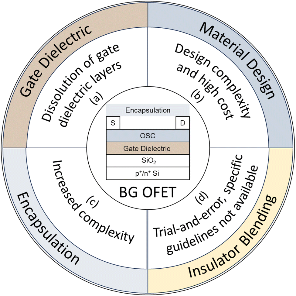 | ||
| Fig. 1 Common methods and issues in achieving water-resistant BG OFETs and the insulator blending method. | ||
We propose that the insulator blending method could mitigate some of the disadvantages associated with the aforementioned methods. This approach is integrated and streamlined, eliminating the need for additional post-fabrication encapsulation. While this approach has been extensively employed in OFETs,24,25 organic photovoltaics (OPVs),26,27 and organic light-emitting diodes (OLEDs),28 it has yet to significantly impact the field (Fig. 1d). Additionally, there is still a lack of systematic and in-depth research on the water durability of OFETs, especially for n-type ones.29–31 In this work, we investigated the blending of a prototypical n-type OSC polymer, PNDI2OD-2T, with a commercially available insulating polymer, polystyrene (PS), of varying chain lengths. The stability of the channel against moisture ingress is significantly improved through the rational modulation of insulator molecular weights (MWs), effectively mitigating moisture-induced energetic disorder and allowing these OFETs to maintain functionality even when submerged in boiling water for a whole day. To unravel the origin of the MW-dependent performance, the phase behaviors of different binary systems were analyzed using in situ absorption spectroscopy, surface energy and depth-profiling X-ray photoelectron spectroscopy (XPS). Our findings indicate that the short-chain PS (MW of several kDa) incorporated OSC–insulator binary system shows a stronger inclination toward vertical phase separation. While blends with higher MW PS exhibit less pronounced vertical phase separation behaviors, potentially limiting their effectiveness in moisture protection. This improvement was consistent across other host OSCs with different bandgaps, demonstrating the universality of this approach. This work not only advances our understanding of the phase behavior in OSC–insulator blended systems but also establishes a facile and effective guideline for enhancing the environmental stability of BG OFETs, thereby broadening their potential for practical applications.
2. Results and discussion
2.1 OFET performance and water stability
Fig. 2a shows the chemical structures of selected representative n-type and p-type OSCs, including two n-type conjugated polymers PNDI2OD-2T and PDI2T, an n-type small molecule Y6, and a p-type polymer PM6. For this investigation, three different types of PS with MWs ranging from 4 kDa to 1000 kDa were sourced from commercial vendors (Fig. 2b). Each OSC solution was blended with an insulator solution, maintaining a specific weight ratio tailored to each OSC material. We sequentially spin-coated both neat OSC and PS-blended films on SiO2/Si wafers directly to fabricate bottom-gate top-contact OFETs, as shown schematically in Fig. 2c. The fabricated devices were then soaked in water at various temperatures (25 °C, hot water at 50 °C and boiling water up to 100 °C) for one day. After immersion, the devices were taken out to test their electrical performance. Detailed fabrication procedures can be found in the Experimental section. | ||
| Fig. 2 Molecular structures of (a) the organic semiconductors (OSCs) (n-type: PNDI2OD-2T, PDI2T and Y6; p-type: PM6) and (b) the insulator involved in this study. (c) Schematic illustration of the blending procedure for fabricating BG OFET and the water-immersion stability test of the studied devices. | ||
Initially, n-type PNDI2OD-2T was used as a model host system. BG OFETs were fabricated using neat PNDI2OD-2T film and films blended with each PS variant, maintaining a weight ratio of 1![[thin space (1/6-em)]](https://www.rsc.org/images/entities/char_2009.gif) :1 (other weight ratios are shown in Fig. S1†). As shown in Fig. 3a and b, the blended OFETs, particularly those with 4 and 400 kDa PS, generally demonstrated significantly enhanced OFET properties, with electron mobilities (μe) ranging from 10−2 to 10−3 cm2 V−1 s−1, compared to the neat PNDI2OD-2T film sample (their output characteristics can be found in Fig. S2†). Notably, the blend incorporating PS with a MW of 4 kDa achieved the highest μe, approximately 2.5 × 10⁻² cm2 V−1 s−1, comparable to the values reported for other PNDI2OD-2T-based BG OFETs.32–34 The 4 kDa PS blending also remarkably improved other OFET characteristics, delivering a twentyfold increase in on current (from 1 × 10⁻⁶ to 2 × 10⁻⁵ A) and a substantial reduction in threshold voltage (VTH) (from 15.6 to 3.7 V) compared to the neat (without PS) device (Table S1†). This improvement via insulator incorporation has been observed in several prior studies by other researchers and may be attributed to suppressed charge trapping at the OSC–dielectric interface.35,36 The defect state density at this interface, calculated from the extracted subthreshold swing, further confirms the positive impact of the 4 kDa PS blend on defect suppression (Table S1†). Conversely, blends using higher MW PS exhibited fewer improvements in transistor performance. μe is down to 1.5 × 10⁻³ cm2 V−1 s−1 when the PS MW reaches 1000 kDa, accompanied by a large shift in VTH and subthreshold swing (Table S1†). To assess water stability, the prepared OFET samples were immersed in water at different temperatures for 24 h. For room temperature (25 °C) water immersion, μe for neat PNDI2OD-2T films, and those blended with 400 kDa and 1000 kDa, was reduced by approximately half an order of magnitude when compared to their fresh counterparts (Fig. 3b and S3†). Interestingly, OFETs fabricated from 4 kDa PS blend demonstrated excellent water resistance, showing negligible changes in μe after one day of water immersion (Fig. 3c). Subsequently, we subjected the OFETs to hot water baths at 50 °C and boiling water at 100 °C for 24 h (Fig. S3f†). As is shown in Fig. 3b, μe decreased as the water temperature gradually rose. For the neat sample, μe progressively declined, retaining only 26% of the original mobility at 50 °C and just 10% at 100 °C. Remarkably, μe of the 4 kDa PS-blended OFETs experienced only a slight decrease after hot/boiling water treatment, highlighting the crucial role of the insulator in enhancing the high-temperature water stability of OFETs. The excellent operational stability may arise from the improved interface between OSC and dielectric, which will be discussed later. To further explore this insulator blending approach, we validated its applicability by extending our observations to other representative p- and n-type OSC systems, blending them with low MW PS in BG OFETs.37,38 The optimized blend ratio and device parameters are detailed in Table S2.† Notably, the achieved mobility values are comparable to those reported for their BG OFETs. Similar to the observations made with PNDI2OD-2T, the performances of blend films based on PDI2T, Y6 and PM6 systems were significantly enhanced in comparison to their neat counterparts, as shown in Fig. 3d–f. Even after room-temperature water immersion for a day, these blended devices successfully retailed their electrical properties, unlike neat OFETs, which experienced clear threshold voltage shifts (ΔVTH) towards the direction of the applied gate voltage. Fig. 3g summarizes the changes in ΔVTH after immersion across different host systems. It is evident that ΔVTH drops significantly following insulator optimizations. For example, adding PS lowers the ΔVTH of neat PDI2T OFETs from 13.5 V to 1.8 V. This outcome demonstrates that the strategy of blending appropriate insulators with OSCs to be water resistant is broadly applicable across different OSC systems, confirming its potential for enhancing the robustness of OFETs in moisture-exposed environments.
:1 (other weight ratios are shown in Fig. S1†). As shown in Fig. 3a and b, the blended OFETs, particularly those with 4 and 400 kDa PS, generally demonstrated significantly enhanced OFET properties, with electron mobilities (μe) ranging from 10−2 to 10−3 cm2 V−1 s−1, compared to the neat PNDI2OD-2T film sample (their output characteristics can be found in Fig. S2†). Notably, the blend incorporating PS with a MW of 4 kDa achieved the highest μe, approximately 2.5 × 10⁻² cm2 V−1 s−1, comparable to the values reported for other PNDI2OD-2T-based BG OFETs.32–34 The 4 kDa PS blending also remarkably improved other OFET characteristics, delivering a twentyfold increase in on current (from 1 × 10⁻⁶ to 2 × 10⁻⁵ A) and a substantial reduction in threshold voltage (VTH) (from 15.6 to 3.7 V) compared to the neat (without PS) device (Table S1†). This improvement via insulator incorporation has been observed in several prior studies by other researchers and may be attributed to suppressed charge trapping at the OSC–dielectric interface.35,36 The defect state density at this interface, calculated from the extracted subthreshold swing, further confirms the positive impact of the 4 kDa PS blend on defect suppression (Table S1†). Conversely, blends using higher MW PS exhibited fewer improvements in transistor performance. μe is down to 1.5 × 10⁻³ cm2 V−1 s−1 when the PS MW reaches 1000 kDa, accompanied by a large shift in VTH and subthreshold swing (Table S1†). To assess water stability, the prepared OFET samples were immersed in water at different temperatures for 24 h. For room temperature (25 °C) water immersion, μe for neat PNDI2OD-2T films, and those blended with 400 kDa and 1000 kDa, was reduced by approximately half an order of magnitude when compared to their fresh counterparts (Fig. 3b and S3†). Interestingly, OFETs fabricated from 4 kDa PS blend demonstrated excellent water resistance, showing negligible changes in μe after one day of water immersion (Fig. 3c). Subsequently, we subjected the OFETs to hot water baths at 50 °C and boiling water at 100 °C for 24 h (Fig. S3f†). As is shown in Fig. 3b, μe decreased as the water temperature gradually rose. For the neat sample, μe progressively declined, retaining only 26% of the original mobility at 50 °C and just 10% at 100 °C. Remarkably, μe of the 4 kDa PS-blended OFETs experienced only a slight decrease after hot/boiling water treatment, highlighting the crucial role of the insulator in enhancing the high-temperature water stability of OFETs. The excellent operational stability may arise from the improved interface between OSC and dielectric, which will be discussed later. To further explore this insulator blending approach, we validated its applicability by extending our observations to other representative p- and n-type OSC systems, blending them with low MW PS in BG OFETs.37,38 The optimized blend ratio and device parameters are detailed in Table S2.† Notably, the achieved mobility values are comparable to those reported for their BG OFETs. Similar to the observations made with PNDI2OD-2T, the performances of blend films based on PDI2T, Y6 and PM6 systems were significantly enhanced in comparison to their neat counterparts, as shown in Fig. 3d–f. Even after room-temperature water immersion for a day, these blended devices successfully retailed their electrical properties, unlike neat OFETs, which experienced clear threshold voltage shifts (ΔVTH) towards the direction of the applied gate voltage. Fig. 3g summarizes the changes in ΔVTH after immersion across different host systems. It is evident that ΔVTH drops significantly following insulator optimizations. For example, adding PS lowers the ΔVTH of neat PDI2T OFETs from 13.5 V to 1.8 V. This outcome demonstrates that the strategy of blending appropriate insulators with OSCs to be water resistant is broadly applicable across different OSC systems, confirming its potential for enhancing the robustness of OFETs in moisture-exposed environments.
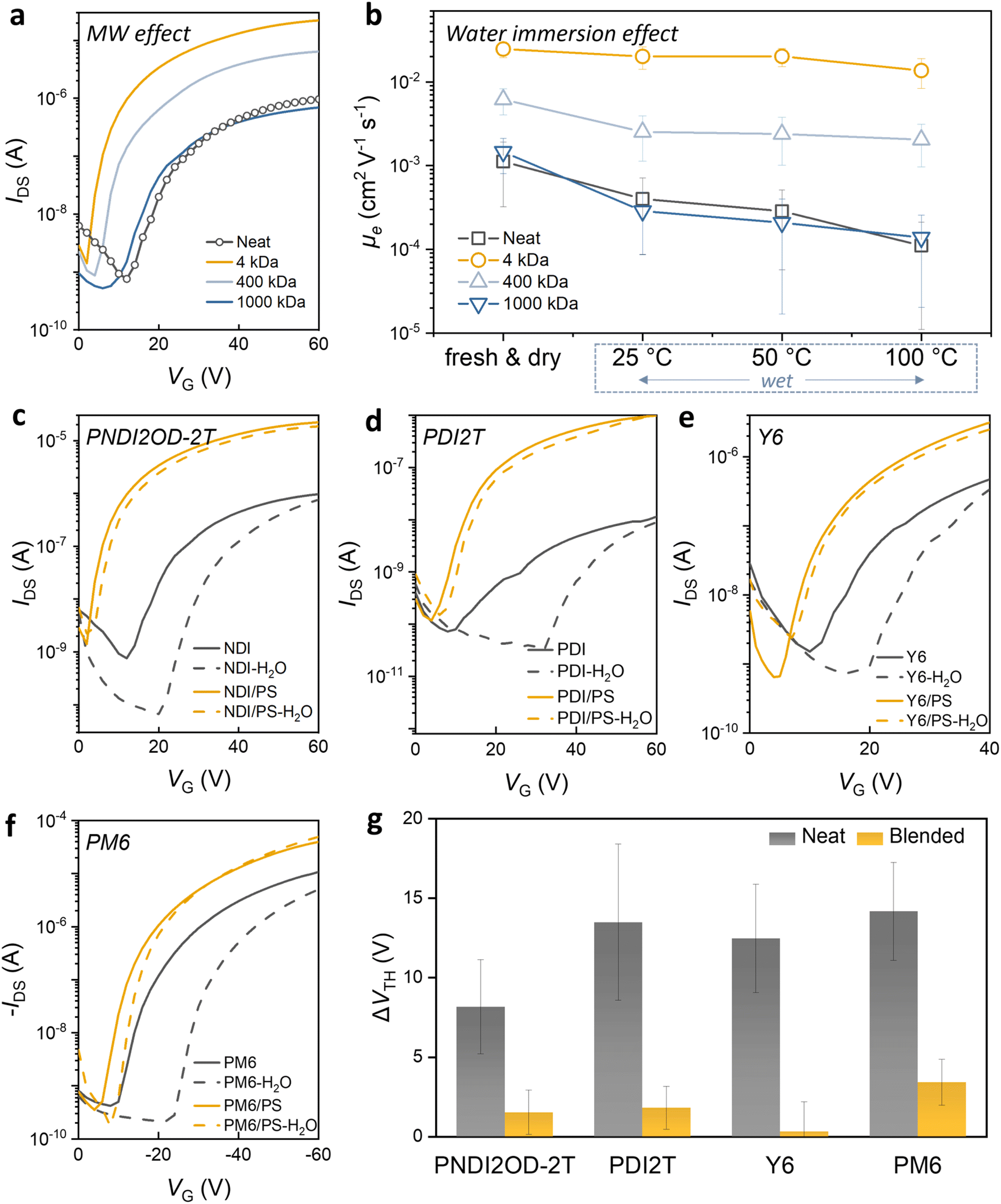 | ||
| Fig. 3 (a) Transfer characteristics of OFETs fabricated with neat PNDI2OD-2T and blended films of varying PS MWs, VDS = 40 V. (b) Mobility changes of neat and different blended OFETs before (fresh & dry) and after one-day water immersion at different temperatures (wet). The data shown are the mean values of 8 devices. Transfer characteristics of neat and 4 kDa PS blended transistors (solid lines), along with those of one-day water-soaked devices (dashed lines) for (c) PNDI2OD-2T (VDS = 40 V), (d) PDI2T (VDS = 40 V), (e) Y6 (VDS = 40 V), and (f) PM6 (VDS = −60 V) systems. (g) VTH shift after one day of water immersion at room temperature. The data shown are the mean values of 8 devices. | ||
To elucidate the water resistance mechanism of OFETs, the photoluminescence (PL) mapping images were utilized to analyze the surface morphology of both neat and optimized blended films before and after one-day water immersion, with results shown in Fig. 4a–d. The initial PL maps of the 4 kDa blended film displayed higher intensities and a more uniform and dense distribution over the entire scanning region (50 × 50 μm2) compared to the neat film. After being soaked in water for a day, the PL intensity of the blended films remained stable with no clear changes observed, superior to that of the neat film whose intensity decreased and was more dispersed. This indicates that proper blending with PS can markedly improve the water stability of organic films, consistent with the findings from optical microscopy, atomic force microscopy, and absorption spectra shown in Fig. S4–S6,† respectively. To explore the underlying cause of the observed stability in blended films, we employed photothermal deflection spectroscopy (PDS) at absorption levels as low as 10−4 to quantitatively evaluate the energetic disorder induced by water immersion.39 It measures the variations in the thermal state of the samples resulting from the nonradiative relaxation of photoexcited carriers. This technique is widely used to characterize defect states in amorphous and organic semiconductors.40–42 The PDS spectra of neat and blended films, with and without water immersion, were depicted in Fig. 4e and f. The Urbach energy (EU), which offers insights into the band tail states at the conduction band edge, was initially extracted from the slope of the absorption tail in the PDS spectra ( , where α0 is the absorption coefficient at the bandgap energy Eg, and hν is the photon energy).43 The inset table in Fig. 4f displays the extracted EU values. For the fresh samples, EU was 30.9 meV for the neat film and 28.9 meV for the blend, showing comparable levels of band edge disorder. These values align with those reported in previous studies.44 After water soaking, the EU rose to 33.6 meV in the control sample, suggesting an increase in disorder, while the blend remained stable at 29.8 meV. Moreover, the sub-band-gap absorption spectrum of the neat film (mainly in the 1.2 to 1.3 eV range) increased significantly upon water exposure compared to its fresh one, suggesting a higher density of defect states.45,46 PDS results reveal that water exposure increases defect states in PNDI2OD-2T, bringing structural and energetic disorder. Conversely, when optimized with PS, the defect state of the film remained relatively stable, corroborating the earlier finding that PS enhances the water stability of the film.
 | ||
| Fig. 4 Photoluminescence (PL) mapping of fresh films: (a) neat and (b) 4 kDa PS blend. PL mapping after one-day water immersion: (c) neat and (d) 4 kDa PS blend. The scanned region is 50 × 50 μm2. Photothermal deflection spectroscopy (PDS) of (e) neat PNDI2OD-2T and (f) blended films, with (solid dots) and without (open dots) water immersion. Linear fits for fresh (solid line) and water-soaked (dashed line) samples are used to determine the Urbach energy (EU). The colored region under the curve denotes increased absorption after water immersion, especially in the control sample, indicative of trap states formation due to water ingress. | ||
2.2 Film formation mechanism
The significant differences in water stability between neat films and those blended with various insulators may be attributed to the differing degrees of phase separation in the polymeric blends during film formation.25 The spatial distribution of polymers in the system greatly depends on the surface energy of the components and their interfacial energy with the substrate.47 The surface energies were calculated using the Wu model (harmonic mean) via contact angle test and presented in Fig. 5a (details are provided in Fig. S7 and Table S3†).48 The neat PNDI2OD-2T film possesses the lowest surface energy of 28.2 mJ m−2, compared to approximately 40 mJ m−2 for the PS materials. The effect of substrate surface tension on phase stratification was also examined by evaluating the interfacial energies with the SiO2 substrate for each component (Fig. 5a and Table S3†), with calculation details provided in the ESI.† The interfacial energy was minimized when the dispersion and polar components of the interacting materials were similar, indicating enhanced interaction and a more stable interface.49 The interfacial tension between PNDI2OD-2T and SiO2 (18 mJ m−2) is higher than that between PS and SiO2 (∼14 mJ m−2), therefore a top PNDI2OD-2T layer is preferentially formed rather than segregation directly on the SiO2 substrate.50 However, the MW variations in PS did not significantly affect the surface energy.49 The differences in performance require further investigation.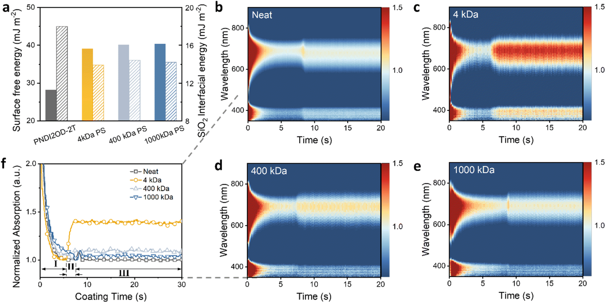 | ||
| Fig. 5 (a) Calculated surface energy values of the materials (closed bars) and their interfacial energies with SiO2 substrate (shaded bars). Time-dependent contour maps of in situ UV-vis absorption spectra during the spin coating process for (b) neat PNDI2OD-2T, (c) 4 kDa, (d) 400 kDa and (e) 1000 kDa PS blended binary systems. (f) Changes in the intensity of the ∼705 nm absorption peak over the coating time, derived from in situ absorption measurements for neat and blended systems. | ||
Therefore, we examined the film formation process during spin-coating of PS blends with varying MWs. The aggregation behaviors of molecules in neat and different blend films were thoroughly analyzed using in situ UV-vis absorption spectroscopy. The absorption spectrum contour maps are visually presented in Fig. 5b–e. Compared to other systems, the incorporation of 4 kDa PS significantly enhanced the absorption intensity, particularly after 6 s of spin-coating (Fig. 5c). To quantify these dynamics, Fig. 5f shows the normalized absorption at approximately 705 nm (the typical absorption peak of PNDI2OD-2T) as a function of coating time for various films.51,52 The film formation process generally encompasses three stages, aligning with previous literature.53,54 In stage I, the absorbance drops rapidly upon spinning due to the flying off of the excess materials dissolved in the solvent. This is followed by stage II, where a low-absorbance region appears, indicative of the coexistence of the solvent and polymer aggregates. By approximately 8 s, a stable absorbance plateau is reached (stage III), signaling the solidification of aggregates. The degree of molecule aggregation, referred to as the aggregation ratio, can be determined by comparing the absorption ratio between the dry film (stage III) and the wet film (stage II). It is observed that both the neat film and those blended films with high MW PS (400 and 1000 kDa) display an aggregation ratio close to one, suggesting minimal change in aggregation during the solvent evaporation process. However, the blend incorporating 4 kDa PS showed a significantly highest aggregation ratio of 1.4, demonstrating accelerated molecular aggregation of PNDI2OD-2T. The enhanced aggregation can be attributed to low viscosity and reduced molecular entanglement of the short-chain insulator, which facilitates more rapid diffusion and aggregation of the PNDI2OD-2T molecules within the blend matrix. The high aggregation ratio may also stem from the limited miscibility between the two materials, potentially leading to distinct phase separation.53,55 In contrast, the aggregation of PNDI2OD-2T in higher MW systems is weak, and the minimal phase separation promotes a more homogenous distribution of the semiconducting polymer throughout the film. Overall, the degree of PNDI2OD-2T aggregation influenced by the MW of the insulator could reflect the phase separation behavior of the binary system. The effects of different insulator MWs vary; notably, short-chain PS significantly enhances the OSC aggregation.
2.3 Model for water-tolerant BG OFETs with MW-dependent insulator blends
To analyze the phase separation behaviors driven by thermodynamic miscibility, the ternary phase diagram was calculated based on the Flory–Huggins model for mixtures of PNDI2OD-2T, 4 kDa PS, and chlorobenzene (CB) solvent (Fig. 6a).56 The calculation details can be found in the ESI.† In general, the location of solvent in different polymer phases significantly influences the morphology of the ternary system, thereby impacting the performance of the material across various applications.57 In Fig. 6a, the right side of the tie lines is higher than the left, indicating a preference for the solvent to reside in the PS region, resulting in higher solvent concentration compared with PNDI2OD-2T. This scenario may lead to the PNDI2OD-2T region forming a more compact and aggregated structure due to its lower solubility, in alignment with in situ analysis showing significant aggregation of OSC molecules in a low MW-based system. With lower surface tension, PNDI2OD-2T tends to migrate to the solution/air interface, while the PS component, with higher affinity for the substrate, moves to the solution/substrate interface to reach thermodynamic equilibrium and minimize the free energy of the system.58 Conversely, the weaker aggregation of PNDI2OD-2T domains in systems including high MW PS (400 and 1000 kDa) may result in more evenly distributed or complex morphology, which can affect material performance in various applications.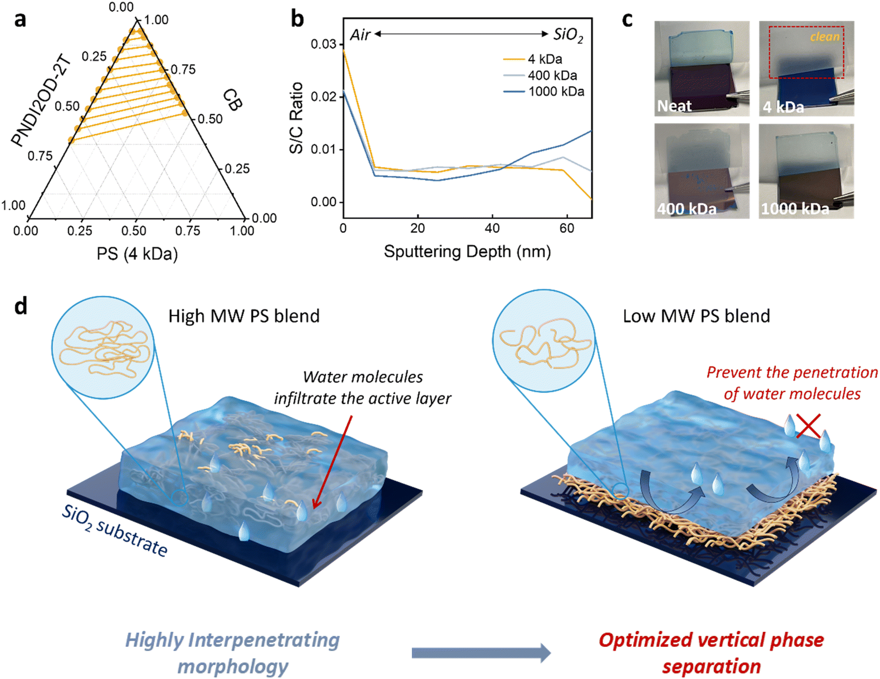 | ||
| Fig. 6 (a) Ternary phase diagram of PNDI2OD-2T/4 kDa PS/solvent mixtures. The binodal is derived at the chemical potential equilibrium of two liquid phases, with tie lines connecting compositions of equal chemical potentials. (b) X-ray photoelectron spectroscopy (XPS) depth profile of the S/C ratio in PNDI2OD-2T/PS blended films with varying PS MWs, from the air surface to the SiO2 interface. The sharp drop in the S/C ratio in the 4 kDa blend sample indicates PS is concentrated in the bottom layer, approaching the substrate. (c) Photographs of the peeling-off process for neat, 4 kDa, 400 kDa and 1000 kDa PS blended films. The 4 kDa PS blended film remained adhered to the substrate, while the neat, 400 kDa and 1000 kDa PS blended film were peeled off with tape. (d) Schematic diagram of the OSC film (blue block) blended with different MW PS (yellow lines) to enhance water stability. The drop shape denotes water molecules. | ||
To validate the presence of a vertically phase-separated structure in low MW insulator blend film, we conducted depth-profiling XPS. The ratio of sulfur S(2p) to carbon C(1s) signals was monitored to estimate the distribution of PNDI2OD-2T (uniquely contains sulfur) along the height direction of the blend film. As shown in Fig. 6b, the content of PNDI2OD-2T is high at the air–solid interface of the blend films, consistent with the previous surface energy analysis. Notably, in the 4 kDa PS blend film, PNDI2OD-2T is predominately distributed at the surface, supporting earlier analyses of vertical segregation structure. In contrast, the 1000 kDa PS blend shows increased PNDI2OD-2T concentration near the sample surface and substrate, with no obvious homogeneous gradient distribution of the semiconducting polymer from the top surface to the bottom (Fig. S8†). Further evidence of vertical phase separation is provided by thin film peel-off tests (Fig. 6c). Films directly coated on SiO2/Si wafers were delaminated using the scotch tape.59,60 As seen, films made from neat and high MW blends (400 kDa and 1000 kDa) were easily peeled off completely from the substrate, likely due to the insufficient interaction between the active layer and the substrate. Whereas the 4 kDa blended film demonstrates strong adhesion to the substrate, rendering it resistant to detachment by tape. This enhanced adhesion can be attributed to the maximized van der Waals forces at the interface between well-developed low MW PS and SiO2 substrate. The peeling test revealed different segregation patterns when PNDI2OD-2T was blended with PS of varying MWs. Interface reinforcement through proper insulator blending can effectively prevent layer delamination, which offers potential benefits for flexible electronic applications.61
Based on the above results, a schematic diagram of OSC films blended with low and high MW insulators was proposed in Fig. 6d. In the OSC and high MW PS blended film, there is a greater intermixed phase near the SiO2 dielectric interface. The partially exposed SiO2 surface (not covered by PS) may adsorb and bind water molecules, potentially forming a monolayer of adsorbed water and deprotonated silanol. These could affect local electrostatic interactions and act as trapping sites for charge carriers, leading to device performance degradation.11 Conversely, the low MW insulating polymer preferentially deposits at the bottom of the two-component blend, serving as a protective barrier over the buried polar dielectric SiO2 layer. The hydrophobic nature of the overlying PS layer hinders water molecules diffusion into the SiO2 layer, avoiding performance issues associated with charge trapping by water. It is further supported by the changes in the cross-sections of neat PNDI2OD-2T and blended films in response to water soaking using scanning electron microscopy. In Fig. S9,† after a whole day of water soaking, significant voids appeared at the polymer/substrate interface in both neat and 1000 kDa blended systems, as highlighted by the red circles. These macroscopic defects at the grooves of the bottom interface clearly contribute to charge trappings and subsequent device degradation, aligning with previous observations of unstable OFET performance following water ingress. Conversely, the polymer/substrate interface in the 4 kDa system remained compact after water immersion, indicating that the low MW PS effectively stabilizes at the buried interface.
3. Conclusions
In conclusion, our study presents a facile means for formulating a water-tolerant active layer in BG OFETs through the strategic blending of PS. Crucially, the choice of MW of the PS has a decisive role in the device performance and water tolerance, with short-chain PS, proving optimal. This preference is attributed to the favorable vertical phase separation between PS and OSC components driven by thermodynamic considerations. The segregated non-polar PS layer at the bottom not only enhances the moisture barrier of the OFET but also facilitates efficient charge transport in the overlying OSC layer. As a result, devices fabricated using this methodology demonstrate robust operational integrity, maintaining stable channel characteristics even after immersion in boiling water for an entire day. These findings suggest the broad applicability of this insulator blending approach in developing water-tolerant devices for solution-processable organic electronics, potentially expanding their use in environments that demand durable performance.4. Experimental methods
4.1 Materials
PNDI2OD-2T (MW = 130 kDa), PDI2T (MW = 50–100 kDa), Y6, and PM6 (MW = 93 kDa) were sourced from 1-Material Inc. It is worth mentioning that the higher MW PNDI2OD-2T provides a more significant improvement in water tolerance (Fig. S10†). PS of varying MW were procured from Polymer Source Inc. All materials were directly used without further modification. The chemical full names are listed in the ESI.† The solutions of PNDI2OD-2T, PDI2T, Y6, and PM6 were prepared by dissolving them at a concentration of 10 mg mL−1 in anhydrous chlorobenzene, chlorobenzene, chloroform, and 1,2-dichlorobenzene, respectively. The blends of PNDI2OD-2T:PS, PDI2T:PS, Y6:PS, and PM6:PS blends were prepared at weight ratios of 1:1, 3:7, 4:1, and 1:1, respectively.
4.2 Device and thin film fabrication
Single-side etched SiO2/Si wafers were placed into an ultrasonic bath and cleaned using deionized water, acetone, and isopropyl alcohol for 15 min each. After being dried with compressed air, the substrates were moved to a nitrogen-filled glovebox to spin coat the neat OSC and blend layers. For PNDI2OD-2T, it was spin-coated at 1500 rpm, then annealed at 120 °C for 20 min. PDI2T was spin-coated at a speed of 2000 rpm and annealed at 80 °C for 20 min. Y6 was spin-coated at a speed of 1500 rpm and annealed at 110 °C for 10 min. PM6 was spin-coated at 2000 rpm and annealed at 200 °C for 20 min. Subsequently, PDINO film was then coated at 5000 rpm to optimize charge extraction. A golden layer (∼100 nm thick) was vacuum evaporated using an Edwards AUTO 306 high vacuum system to define the source–drain electrodes through a shadow mask.4.3 Characterization
OFET electrical measurements were taken in a low-vacuum cryostat (Oxford Instruments, Optistat DN-V) at ambient temperature, using a Keithley 236 source measurement unit linked with a Xantrex XT 120–0.5 to supply the voltage. The field-effect mobility and threshold voltage were calculated from the transfer characteristics in the saturation regime. The potential reduction in capacitance due to the insulator is not considered, as the theoretical change in film thickness is estimated to be less than 5% of the total capacitance, which may slightly underestimate the mobility and suggest the actual mobility are slightly higher than reported.62 For the water immersion test, the devices were submerged in deionized water at different temperatures and then dried with compressed air prior to testing to ensure accurate results. The PL mapping data were collected using Witec alpha300 R with a 532 nm laser excitation. Photothermal deflection spectroscopy (PDS): Employed a 1 kW Xe arc lamp and a ¼ m grating monochromator (Oriel) with a pump beam modulated at 13 Hz by a mechanical chopper. The sample, immersed in perfluorohexane as a deflection fluid, was irradiated by a parallel probe beam (He–Ne laser, Uniphase, Model 1103P). Deflection signals of the probe beam were captured by a TEMic position sensor and processed with a Stanford Research SR830 lock-in amplifier, normalizing PDS absorption spectra to the pump power. UV-vis spectroscopy: UV-vis absorption measurements were carried out using a QE Pro 2000 spectrometer equipped with a tungsten halogen lamp (Filmetrics, Inc.) and an LED light source. The integration time was 100 ms for each spectrum during the film coating. The detailed experimental setup has been described elsewhere.63 Contact angle: the contact angle test was performed by an OCA 20LHT Micro contact angle analyzer. The depth-profiling XPS test was performed on PHI Model 5802 by using an Ar+ sputtering gun operated at 2 keV.Data availability
The data supporting this article have been included as part of the ESI.†Author contributions
Z. Z. and S. K. S. conceived the ideas and coordinated the research. Z. Z. carried out the device fabrication and characterizations. Z. Z., Y. W. and C. Z. analyzed the experimental data and wrote the original manuscript. Y. W. and S.-W. T. performed in situ optical tests. W. X., Y. T. and H. Y. conducted phase diagram calculation. Y. H., T. W. and S. K. S. revised the manuscript.Conflicts of interest
There are no conflicts to declare.Acknowledgements
C. Z. acknowledges the National Natural Science Foundation of China (52403259) and Postdoctoral Fellowship Program of CPSF (GZC20233148). Z. Z. thanks Run Shi for insightful discussions on data analysis.References
- T. Yokota, P. Zalar, M. Kaltenbrunner, H. Jinno, N. Matsuhisa, H. Kitanosako, Y. Tachibana, W. Yukita, M. Koizumi and T. Someya, Sci. Adv., 2016, 2, e1501856 CrossRef PubMed.
- M. Kaltenbrunner, T. Sekitani, J. Reeder, T. Yokota, K. Kuribara, T. Tokuhara, M. Drack, R. Schwödiauer, I. Graz, S. Bauer-Gogonea, S. Bauer and T. Someya, Nature, 2013, 499, 458–463 CrossRef CAS PubMed.
- Y. Van De Burgt, A. Melianas, S. T. Keene, G. Malliaras and A. Salleo, Nat. Electron., 2018, 1, 386–397 CrossRef.
- S. Fratini, M. Nikolka, A. Salleo, G. Schweicher and H. Sirringhaus, Nat. Mater., 2020, 19, 491–502 CrossRef CAS PubMed.
- T. D. Anthopoulos, Y.-Y. Noh and O. D. Jurchescu, Adv. Funct. Mater., 2020, 30, 2001678 CrossRef CAS.
- C. Zhang, P. Chen and W. Hu, Chem. Soc. Rev., 2015, 44, 2087–2107 RSC.
- B. Kumar, B. K. Kaushik and Y. S. Negi, Polym. Rev., 2014, 54, 33–111 CrossRef CAS.
- R. Häusermann and B. Batlogg, Appl. Phys. Lett., 2011, 99, 083303 CrossRef.
- L.-L. Chua, J. Zaumseil, J.-F. Chang, E. C.-W. Ou, P. K.-H. Ho, H. Sirringhaus and R. H. Friend, Nature, 2005, 434, 194–199 CrossRef CAS PubMed.
- A. M. Schrader, J. I. Monroe, R. Sheil, H. A. Dobbs, T. J. Keller, Y. Li, S. Jain, M. S. Shell, J. N. Israelachvili and S. Han, Proc. Natl. Acad. Sci. U. S. A., 2018, 115, 2890–2895 CrossRef CAS PubMed.
- H. F. Iqbal, M. Waldrip, H. Chen, I. McCulloch and O. D. Jurchescu, Adv. Electron. Mater., 2021, 7, 2100393 CrossRef CAS.
- J. Kim, J. Jang, K. Kim, H. Kim, S. H. Kim and C. E. Park, Adv. Mater., 2014, 26, 7241–7246 CrossRef CAS PubMed.
- Y. Baek, S. Lim, E. J. Yoo, L. H. Kim, H. Kim, S. W. Lee, S. H. Kim and C. E. Park, ACS Appl. Mater. Interfaces, 2014, 6, 15209–15216 CrossRef CAS PubMed.
- W.-Y. Sit, S. H. Cheung, C. Y. H. Chan, K. K. Tsung, S. W. Tsang and S. K. So, Adv. Electron. Mater., 2016, 2, 1500273 CrossRef.
- S. H. Kim, S. Nam, J. Jang, K. Hong, C. Yang, D. S. Chung, C. E. Park and W.-S. Choi, J. Appl. Phys., 2009, 105, 104509 CrossRef.
- C. Li, J. Zhang, Z. Li, W. Zhang, M. S. Wong and G. Yu, J. Mater. Chem. C, 2019, 7, 297–301 RSC.
- Y. Cho, H. R. Lee, A. Jeong, J. Lee, S. M. Lee, S. H. Joo, S. K. Kwak, J. H. Oh and C. Yang, ACS Appl. Mater. Interfaces, 2019, 11, 40347–40357 CrossRef CAS PubMed.
- D. Yoo, Y. Kim, M. Min, G. H. Ahn, D.-H. Lien, J. Jang, H. Jeong, Y. Song, S. Chung, A. Javey and T. Lee, ACS Nano, 2018, 12, 11062–11069 CrossRef CAS PubMed.
- K. Bulgarevich, K. Sakamoto, T. Yasuda, T. Minari and M. Takeuchi, Adv. Electron. Mater., 2020, 6, 2000161 CrossRef CAS.
- L. M. Castano and A. B. Flatau, Smart Mater. Struct., 2014, 23, 053001 CrossRef CAS.
- J. Yang, C. Wang, L. Liu, H. Zhang and J. Ma, ACS Appl. Mater. Interfaces, 2022, 14, 21253–21262 CrossRef CAS PubMed.
- X. Ji, P. Zhou, L. Zhong, A. Xu, A. C. O. Tsang and P. K. L. Chan, Adv. Sci., 2018, 5, 1701053 CrossRef PubMed.
- K. Kuribara, H. Wang, N. Uchiyama, K. Fukuda, T. Yokota, U. Zschieschang, C. Jaye, D. Fischer, H. Klauk, T. Yamamoto, K. Takimiya, M. Ikeda, H. Kuwabara, T. Sekitani, Y.-L. Loo and T. Someya, Nat. Commun., 2012, 3, 723 CrossRef PubMed.
- B. Kang, F. Ge, L. Qiu and K. Cho, Adv. Electron. Mater., 2017, 3, 1600240 CrossRef.
- Z. Zhang, R. Shi, A. Amini, S. K. So and C. Cheng, Phys. Status Solidi RRL, 2022, 2100602 CrossRef CAS.
- C. Wang, X. Liu, Y. Xiao, J. Bergqvist, X. Lu, F. Gao and M. Fahlman, Sol. RRL, 2020, 4, 2000261 CrossRef CAS.
- T. A. M. Ferenczi, C. Müller, D. D. C. Bradley, P. Smith, J. Nelson and N. Stingelin, Adv. Mater., 2011, 23, 4093–4097 CrossRef CAS PubMed.
- D. Abbaszadeh, A. Kunz, G. A. H. Wetzelaer, J. J. Michels, N. I. Crăciun, K. Koynov, I. Lieberwirth and P. W. M. Blom, Nat. Mater., 2016, 15, 628–633 CrossRef CAS PubMed.
- A. Giovannitti, C. B. Nielsen, D.-T. Sbircea, S. Inal, M. Donahue, M. R. Niazi, D. A. Hanifi, A. Amassian, G. G. Malliaras, J. Rivnay and I. McCulloch, Nat. Commun., 2016, 7, 13066 CrossRef CAS PubMed.
- O. Knopfmacher, M. L. Hammock, A. L. Appleton, G. Schwartz, J. Mei, T. Lei, J. Pei and Z. Bao, Nat. Commun., 2014, 5, 2954 CrossRef PubMed.
- Z. Zhang, J. K. W. Ho, C. Zhang, H. Yin, Z. Wen, G. Cai, R. Zhao, R. Shi, X. Lu, J. Liu, X. Hao, C. Cheng and S. K. So, J. Mater. Chem. C, 2021, 9, 12281–12290 RSC.
- H. Yan, Z. Chen, Y. Zheng, C. Newman, J. R. Quinn, F. Dötz, M. Kastler and A. Facchetti, Nature, 2009, 457, 679–686 CrossRef CAS PubMed.
- H. Wei, Y. Liu, Z. Liu, J. Guo, P.-A. Chen, X. Qiu, G. Dai, Y. Li, J. Yuan, L. Liao and Y. Hu, Adv. Electron. Mater., 2020, 6, 1901241 CrossRef CAS.
- N. Shin, J. Zessin, M. H. Lee, M. Hambsch and S. C. B. Mannsfeld, Adv. Funct. Mater., 2018, 28, 1802265 Search PubMed.
- L. Janasz, M. Borkowski, P. W. M. Blom, T. Marszalek and W. Pisula, Adv. Funct. Mater., 2022, 32, 2105456 CrossRef CAS.
- Z. Zhang, Y. Tang, Y. Wang, Z. Zeng, R. Shi, H. Yan, S.-W. Tsang, C. Cheng and S. K. So, ACS Appl. Mater. Interfaces, 2022, 14, 30174–30181 CrossRef CAS PubMed.
- S. Shoaee, H. M. Luong, J. Song, Y. Zou, T.-Q. Nguyen and D. Neher, Adv. Mater., 2024, 36, 2302005 CrossRef CAS PubMed.
- H. Yin, J. Yan, J. K. W. Ho, D. Liu, P. Bi, C. H. Y. Ho, X. Hao, J. Hou, G. Li and S. K. So, Nano Energy, 2019, 64, 103950 Search PubMed.
- A. Vlk, Z. Remes, L. Landova, K. Ridzonova, R. Hlavac, A. Fejfar and M. Ledinsky, J. Phys. Chem. Lett., 2024, 15, 1273–1278 CrossRef CAS PubMed.
- X. Yan, M. Xiong, X.-Y. Deng, K.-K. Liu, J.-T. Li, X.-Q. Wang, S. Zhang, N. Prine, Z. Zhang, W. Huang, Y. Wang, J.-Y. Wang, X. Gu, S. K. So, J. Zhu and T. Lei, Nat. Commun., 2021, 12, 5723 Search PubMed.
- K.-K. Liu, P. Li, Y. Lei, Z. Zhang, X. Pan, S. K. So and T. Lei, Adv. Funct. Mater., 2023, 33, 2300049 Search PubMed.
- W. B. Jackson and N. M. Amer, Phys. Rev. B:Condens. Matter Mater. Phys., 1982, 25, 5559–5562 Search PubMed.
- C. Zhang, S. Mahadevan, J. Yuan, J. K. W. Ho, Y. Gao, W. Liu, H. Zhong, H. Yan, Y. Zou, S.-W. Tsang and S. K. So, ACS Energy Lett., 2022, 7, 1971–1979 Search PubMed.
- M. Xiao, X. Ren, K. Ji, S. Chung, X. Shi, J. Han, Z. Yao, X. Tao, S. J. Zelewski, M. Nikolka, Y. Zhang, Z. Zhang, Z. Wang, N. Jay, I. Jacobs, W. Wu, H. Yu, Y. Abdul Samad, S. D. Stranks, B. Kang, K. Cho, J. Xie, H. Yan, S. Chen and H. Sirringhaus, Sci. Adv., 2023, 9, eadg8659 Search PubMed.
- S. Wu, J. Zhang, Z. Li, D. Liu, M. Qin, S. H. Cheung, X. Lu, D. Lei, S. K. So, Z. Zhu and A. K.-Y. Jen, Joule, 2020, 4, 1248–1262 CrossRef CAS.
- Y. Cheng, M. Li, X. Liu, S. H. Cheung, H. T. Chandran, H.-W. Li, X. Xu, Y.-M. Xie, S. K. So, H.-L. Yip and S.-W. Tsang, Nano Energy, 2019, 61, 496–504 Search PubMed.
- Y. Liu, D. Tang, K. Zhang, P. Huang, Z. Wang, K. Zhu, Z. Li, L. Yuan, J. Fan, Y. Zhou and B. Song, ACS Omega, 2017, 2, 2489–2498 CrossRef CAS PubMed.
- X. Bulliard, S.-G. Ihn, S. Yun, Y. Kim, D. Choi, J.-Y. Choi, M. Kim, M. Sim, J.-H. Park, W. Choi and K. Cho, Adv. Funct. Mater., 2010, 20, 4381–4387 CrossRef CAS.
- J. H. Lee, J. Lyu, M. Kim, H. Ahn, S. Lim, H. W. Jang, H.-J. Chung, J. H. Lee, J. Koo and W. H. Lee, Adv. Funct. Mater., 2023, 33, 2215221 CrossRef CAS.
- S. Wang, S. Fabiano, S. Himmelberger, S. Puzinas, X. Crispin, A. Salleo and M. Berggren, Proc. Natl. Acad. Sci. U. S. A., 2015, 112, 10599–10604 CrossRef CAS PubMed.
- R. Zhang, Y. Yan, Q. Zhang, Q. Liang, J. Zhang, X. Yu, J. Liu and Y. Han, ACS Appl. Mater. Interfaces, 2021, 13, 21756–21764 CrossRef CAS PubMed.
- Y.-J. Kim, S. Lee, M. R. Niazi, K. Hwang, M.-C. Tang, D.-H. Lim, J.-S. Kang, D.-M. Smilgies, A. Amassian and D.-Y. Kim, ACS Appl. Mater. Interfaces, 2020, 12, 36417–36427 CrossRef CAS PubMed.
- I. Angunawela, M. M. Nahid, M. Ghasemi, A. Amassian, H. Ade and A. Gadisa, ACS Appl. Mater. Interfaces, 2020, 12, 26239–26249 CrossRef CAS PubMed.
- B. Hu, C. Zhang, X. Wang, X. Ding, J. Yu, L. Bu, K. Wang, H. Hu and G. Lu, Chem. Eng. J., 2024, 150968 CrossRef CAS.
- J. Xue, H. B. Naveed, H. Zhao, B. Lin, Y. Wang, Q. Zhu, B. Wu, Z. Bi, X. Zhou, C. Zhao, K. Zhou and W. Ma, J. Mater. Chem. A, 2022, 10, 13439–13447 RSC.
- J. J. Michels, A. Kunz, H. S. Dehsari, K. Asadi and P. W. M. Blom, in Solution-Processable Components for Organic Electronic Devices, ed. J. Ulanski, B. Luszczynska and K. Matyjaszewski, Wiley-VCH Verlag GmbH & Co. KGaA, Weinheim, Germany, 2019, pp. 227–258 Search PubMed.
- X. He, C. C. S. Chan, X. Zou, S. Zhang, P. W. K. Fong, J. Kim, G. Li, X. Hu, W. Ma, K. S. Wong and W. C. H. Choy, Adv. Energy Mater., 2023, 13, 2203697 CrossRef CAS.
- L. Gao, S. Hou, Z. Wang, Z. Gao, X. Yu and J. Yu, Micromachines, 2019, 10, 716 CrossRef PubMed.
- J. Ning, Y. Zhu, Z. Hu, Y. Shi, M. U. Ali, J. He, Y. He, F. Yan, S. Yang, J. Miao and H. Meng, Adv. Funct. Mater., 2020, 30, 2000837 CrossRef CAS.
- H. Lee and C. Lee, Adv. Energy Mater., 2018, 8, 1702197 CrossRef.
- Z. Li, C. Jia, Z. Wan, J. Xue, J. Cao, M. Zhang, C. Li, J. Shen, C. Zhang and Z. Li, Nat. Commun., 2023, 14, 6451 CrossRef CAS PubMed.
- K. Haase, C. Teixeira da Rocha, C. Hauenstein, Y. Zheng, M. Hambsch and S. C. B. Mannsfeld, Adv. Electron. Mater., 2018, 4, 1800076 CrossRef.
- Y. Wang, Z. Zeng, Y. Zhang, Z. Zhang, L. Bi, A. He, Y. Cheng, A. K.-Y. Jen, J. C. Ho and S.-W. Tsang, Adv. Mater., 2024, 36, 2307635 CrossRef CAS PubMed.
Footnotes |
| † Electronic supplementary information (ESI) available. See DOI: https://doi.org/10.1039/d4ta08390c |
| ‡ Equally contributed to this work. |
| This journal is © The Royal Society of Chemistry 2025 |