
A two-step strategy improves the wide-temperature-range thermoelectric performance of Mg3+xBi1.29Sb0.7Te0.01†
Yushuo
Ma‡
a,
Xiao-Lei
Shi‡
b,
Li
Zhang
 *a,
Han
Gao
c,
Meng
Li
b,
Liang-Cao
Yin
d,
Wei-Di
Liu
b,
Qingfeng
Liu
d,
Yan-Ling
Yang
a and
Zhi-Gang
Chen
*b
*a,
Han
Gao
c,
Meng
Li
b,
Liang-Cao
Yin
d,
Wei-Di
Liu
b,
Qingfeng
Liu
d,
Yan-Ling
Yang
a and
Zhi-Gang
Chen
*b
aSchool of Materials Science and Engineering, Shaanxi University of Science & Technology, Xi'an 710021, China. E-mail: zhangli@sust.edu.cn
bSchool of Chemistry and Physics, ARC Research Hub in Zero-emission Power Generation for Carbon Neutrality, and Centre for Materials Science, Queensland University of Technology, Brisbane, Queensland 4000, Australia. E-mail: zhigang.chen@qut.edu.au
cKey Laboratory of Material Physics of Ministry of Education, School of Physics and Microelectronics, Zhengzhou University, Zhengzhou 450052, China
dState Key Laboratory of Materials-Oriented Chemical Engineering, College of Chemical Engineering, Nanjing Tech University, Nanjing 211816, China
First published on 1st March 2025
Abstract
Mg3Bi2-based thermoelectric materials have attracted significant attention due to the absence of volatile and expensive chalcogen elements like Te, along with their potential for high thermoelectric performance near room temperature. However, stabilizing the Mg content and optimizing the preparation process remain key challenges in further improving their thermoelectric properties. In this study, we employ a two-step method to progressively enhance the near-room-temperature performance of Mg3Bi2-based thermoelectric materials. First, by fine-tuning the excess Mg, we achieve a p-to-n type transition, optimizing carrier concentration and mobility, which leads to a substantial improvement in the power factor. Next, by modifying the high-temperature sintering process to create a well-structured microstructure, we increase grain size without compromising the system composition, further enhancing room-temperature electron mobility for faster electron transport. As a result, the room-temperature power factor of Mg3.4Bi1.29Sb0.7Te0.01 sintered at 1073 K significantly increases from 6.5 to 16 μW cm−1 K−2, while the figure of merit value at 323 K increases from 0.2 to nearly 0.5, with the peak figure of merit at 500 K approaching 0.9, reaching one of the highest values reported for similar materials.
Introduction
Thermoelectric materials, which enable the direct conversion of heat into electrical energy, have garnered significant research interest due to their unique energy conversion mechanisms and wide-ranging applications.1 The efficiency of thermoelectric devices is dictated by the performance of these materials,2 typically measured by the dimensionless figure of merit ZT = S2σT/(κl + κe) = S2σT/κ, where S, σ, κl, κe, κ, and T represent the Seebeck coefficient, electrical conductivity, lattice thermal conductivity, electronic thermal conductivity, thermal conductivity, and absolute temperature, respectively.3 Enhancing thermoelectric performance, therefore, requires a high S2σ and low κ.4 Over the past few decades, various thermoelectric materials have been explored, including near-room-temperature materials (e.g., Bi2Te3 and Ag2Q, where Q = S, Se, Te),5–7 mid-temperature materials (e.g., PbSe, SnTe, and GeTe),8–10 and high-temperature materials (e.g., SiGe alloys and half-Heusler alloys),11,12 all of which exhibit relatively high ZT values within their respective temperature ranges. While Bi2Te3, PbTe and SnSe have shown promising performance in near-room- and mid-temperature ranges, their commercialization is hindered by the volatility and toxicity of chalcogen elements (Te, Pb, and Se), along with high production costs.13 Consequently, non-toxic, low-cost Mg3(Sb,Bi)2-based thermoelectric materials have emerged as a promising alternative.14Mg3Sb2-based thermoelectric materials belong to the Zintl phase structure and are distinguished by their low bandgap and low κ.15 The inherently low κl is attributed to the instability of Mg atoms within the layers and the highly disordered quasi-layered crystal structure.16 However, the volatility and high vapor pressure of Mg result in a significant number of Mg vacancies (VMg), which impede electron transport and substantially degrade the thermoelectric performance.17 In 2016, Tamaki et al.18 successfully achieved n-type conductive Mg3Sb2 by introducing excess Mg, while Imasato et al.19 later conducted a more detailed investigation into its thermoelectric properties at varying Mg contents. Studies have shown that excess Mg and electron doping can achieve stable n-type conductivity.20 The multi-valley characteristic of n-type conductivity notably improves its electrical transport properties compared to p-type, with the highest ZT of Mg3Sb2-based thermoelectric materials being achieved in compositions such as Mg3Sb1.5Bi0.49Te0.01 + 10% Nb21 and Mg3.2In0.005Sb1.5Bi0.49Te0.01.22 However, these high ZT values of Mg3Sb2-based thermoelectric materials occur at elevated temperatures (above 700 K), while their thermoelectric performance in the low-to-mid temperature range remains poor, limiting their effectiveness for near-room-temperature applications.
Researchers have found that introducing Bi into Sb sites can modify the Bi/Sb alloy ratio, reduce the bandgap, and shift the temperature range of high ZT values closer to room temperature.23,24 Bi doping also induces lattice strain, enhancing phonon scattering and lowering the κ. As a result, significant research focusing on n-type thermoelectric materials based on Bi-doped Mg3Sb2 has emerged. To further enhance its thermoelectric performance, researchers are exploring both interface engineering and doping modifications. On one front, researchers optimize grain size and the chemical composition and structure near grain boundaries using techniques such as Mg vapor annealing,25 Nb wetting phases,26 introducing carbon nanotubes at grain boundaries,27 and employing nano-sintering aids like Mg2Cu to lower grain boundary barriers.28 On the other front, researchers enhance electrical properties through doping, such as substituting Sb/Bi sites with S,29 Se,30 or Te,18 or doping the Mg sites with group III and lanthanide elements like Y,31 Sc,32 La,33 and Nd.34 While these doping strategies generally increase the carrier concentration (n), they often impact the carrier mobility (μ). Thus, the challenge remains in optimizing thermoelectric performance without compromising the μ. Additionally, further research into process improvements to enhance the performance of Mg3Bi2 across a wide temperature range continues to be a key focus. While previous research on the sintering process has primarily focused on high Sb compositions,35,36 the low melting point and high volatility of Bi are likely to hinder the Mg3Bi2 alloying process and exacerbate Mg volatility. Therefore, a more detailed investigation of Mg content and the sintering process under high Bi composition is crucial.
In general, achieving stable n-type conductivity requires an excess of Mg, with the required amount depending on the synthesis method. Once the n-type conduction threshold is reached, fine-tuning of Mg content becomes crucial for optimizing the thermoelectric performance. This study highlights a significant enhancement in the wide-temperature-range thermoelectric performance of Mg3Bi2-based materials using a straightforward two-step method. By precisely controlling the Mg content to optimize σ and adjusting the high-temperature sintering process to engineer the microstructure, grain boundary resistance was reduced, and the room-temperature μ was improved, enabling faster electron transport. The results show that the power factor of Mg3.4Bi1.29Sb0.7Te0.01 sintered at 1073 K increased significantly, with the room-temperature S2σ rising from 6.5 to 16 μW cm−1 K−2, nearly a threefold improvement. Due to the remarkable improvement in electrical properties, the ZT value at 323 K increased from 0.2 to nearly 0.5, while the peak ZT at 500 K approached 0.9, reaching one of the highest values reported for similar materials (Table S1, ESI†).30,37–44
Results and discussion
In the experimental process, the issue of increased VMg due to Mg volatilization is typically addressed by introducing excess Mg. The extent of Mg volatilization depends not only on the sintering temperature, heating rate, and holding time but may also be influenced by the Bi/Sb elemental ratio, with higher Bi content increasing the likelihood of Mg volatilization during sintering. To achieve high-performance n-type conductivity near room temperature, it is essential to precisely control the amount of excess Mg and the sintering temperature to optimize the thermoelectric performance and microstructure. This study first investigated the effect of excess Mg levels on the thermoelectric performance and microstructure of the material. To assess the impact of excess Mg on thermoelectric properties, Mg3.2Bi1.3Sb0.7 was selected as the base composition, given its high preliminary S2σ (Fig. S1, ESI†). A small amount of Te (1%) was then doped to regulate n.45–47 The rationality of this composition was first verified using first-principles density functional theory (DFT). Fig. 1 presents the computational results of Mg3Bi2-based thermoelectric compounds, including the calculated band structures of Mg24Bi16, Mg24Bi12Sb4, Mg24Bi12Sb3Te, Mg23Bi12Sb3Te, and Mg25Bi12Sb3Te. In Fig. 1a, the electronic structure of Mg24Bi16 shows an overlap between the conduction band and valence band without a clear direct bandgap, indicating that Mg24Bi16 has an electronic structure similar to that of metals. After partially substituting Bi with Sb, the electronic structure of Mg24Bi12Sb4, as shown in Fig. 1b, exhibits band splitting due to the different electronic orbitals of Bi and Sb. A magnified view in Fig. 1c shows that the conduction band and valence band no longer overlap, and a small direct bandgap emerges, with the bottom of the conduction band and the top of the valence band located at the same position. As the Sb content increases, the direct bandgap progressively widens and eventually transitions into an indirect bandgap, where the bottom of the conduction band and the top of the valence band are positioned at different locations in momentum space, as shown in the electronic structures of Mg24Bi4Sb12 and Mg24Sb16 (Fig. S2a and b, ESI†). In Fig. 1d, the electronic structure of Mg24Bi12Sb3Te shows that Te shifts the Fermi level towards the conduction band, enhancing n-type conductivity in the system. We also examined the effects of VMg and additional Mg atoms (e.g., interstitial Mg, Mgi). Fig. 1e and f illustrate the electronic structures of Mg23Bi12Sb3Te and Mg25Bi12Sb3Te, showing that VMg shifts the Fermi level towards the valence band, indicating a tendency for the system to exhibit p-type conductivity. Conversely, additional Mg atoms (e.g., Mgi) shift the Fermi level towards the conduction band, similar to the effect of Te, promoting n-type conductivity. Thus, ensuring enough Mg to minimize the formation of VMg is one of the primary objectives of this study. However, in actual samples, due to the high volatility of Mg, the nominal composition Mg3Bi1.29Sb0.7Te0.01 may exhibit p-type conductivity due to the presence of VMg. Therefore, the first step in our study focuses on optimizing electrical transport performance by adjusting the amount of excess Mg to achieve stable n-type conductivity.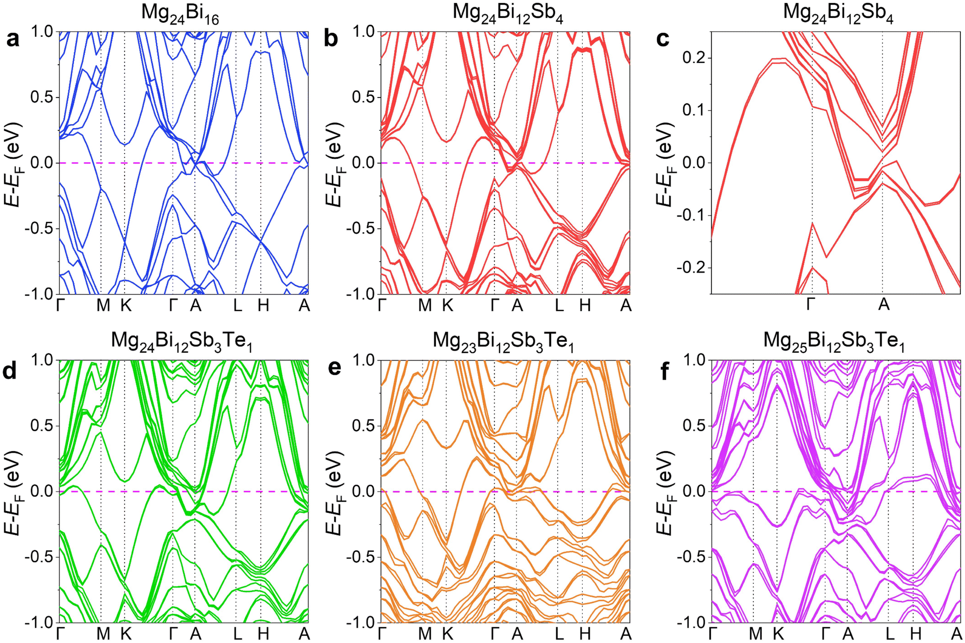 | ||
| Fig. 1 Computational results of Mg3Bi2-based thermoelectric compounds. Calculated band structures of (a) Mg24Bi16, (b) Mg24Bi12Sb4, (c) magnified Mg24Bi12Sb4, (d) Mg24Bi12Sb3Te, (e) Mg23Bi12Sb3Te, and (f) Mg25Bi12Sb3Te. | ||
To explore the optimized excess amount of Mg, we prepared a series of samples with nominal compositions of Mg3+xBi1.29Sb0.7Te0.01 (x = 0.2, 0.3, 0.4, and 0.5). The phase information of these bulk samples was analyzed using room-temperature X-ray diffraction (XRD) after hot-pressing at 973 K, as shown in Fig. 2a. The XRD patterns, recorded over a 2θ range from 20 to 60°, were compared with standard peaks corresponding to pure Mg3Bi2. All diffraction peaks can be indexed to the α-Mg3Bi2 phase with a P![[3 with combining macron]](https://www.rsc.org/images/entities/char_0033_0304.gif) m1 space group and an anti-α-La2O3 structure.42 Within the detection limits, a few minor secondary phase peaks are present, likely attributed to unreacted elemental substances or the MgO secondary phase, which is commonly found in Mg3(Bi, Sb)2 materials.29 However, MgO, as an insulating material, scatters both carriers and phonons, resulting in its effects on and contributions to the thermoelectric properties effectively canceling each other out. Fig. 2b presents the magnified XRD patterns with a 2θ range from 20 to 26°. The diffraction peaks shift to the left as Mg content increases up to x = 0.4, after which the peaks begin to shift to the right. The leftward shift for x < 0.4 is caused by lattice expansion due to the reduction of VMg. However, when x > 0.4, the diffraction peak shifts to the right. This shift can be attributed to changes in the crystal structure, likely caused by modifications in the atomic arrangement within the crystal lattice due to the presence of excess magnesium. Fig. 2c shows a SEM image of the freshly fractured surface of the Mg3.4Bi1.29Sb0.7Te0.01 sample, revealing a dense structure with no visible defects or pores, indicating successful sintering and good material compactness. The sample also exhibits a characteristic layered structure, which originates from its typical rhombohedral crystal structure (space group: Pm1), comprising alternating layers of [Mg2(Sb/Bi)2]2− and Mg2+ ions.30 For further reference, Fig. S3 (ESI†) shows SEM images of fractured surfaces taken from other positions of Mg3.4Bi1.29Sb0.7Te0.01, confirming the presence of uniform layered and dense structures throughout the material.
m1 space group and an anti-α-La2O3 structure.42 Within the detection limits, a few minor secondary phase peaks are present, likely attributed to unreacted elemental substances or the MgO secondary phase, which is commonly found in Mg3(Bi, Sb)2 materials.29 However, MgO, as an insulating material, scatters both carriers and phonons, resulting in its effects on and contributions to the thermoelectric properties effectively canceling each other out. Fig. 2b presents the magnified XRD patterns with a 2θ range from 20 to 26°. The diffraction peaks shift to the left as Mg content increases up to x = 0.4, after which the peaks begin to shift to the right. The leftward shift for x < 0.4 is caused by lattice expansion due to the reduction of VMg. However, when x > 0.4, the diffraction peak shifts to the right. This shift can be attributed to changes in the crystal structure, likely caused by modifications in the atomic arrangement within the crystal lattice due to the presence of excess magnesium. Fig. 2c shows a SEM image of the freshly fractured surface of the Mg3.4Bi1.29Sb0.7Te0.01 sample, revealing a dense structure with no visible defects or pores, indicating successful sintering and good material compactness. The sample also exhibits a characteristic layered structure, which originates from its typical rhombohedral crystal structure (space group: Pm1), comprising alternating layers of [Mg2(Sb/Bi)2]2− and Mg2+ ions.30 For further reference, Fig. S3 (ESI†) shows SEM images of fractured surfaces taken from other positions of Mg3.4Bi1.29Sb0.7Te0.01, confirming the presence of uniform layered and dense structures throughout the material.
 | ||
| Fig. 2 Characterization and thermoelectric performance of Mg3+xBi1.29Sb0.7Te0.01. (a) X-ray diffraction (XRD) patterns with a 2θ range from 20 to 60°. (b) Magnified XRD patterns with a 2θ range from 20 to 26°. (c) Scanning electron microscopy (SEM) image of the fractured surface of Mg3.4Bi1.29Sb0.7Te0.01. Temperature-dependent (d) electrical conductivity (σ) and (e) Seebeck coefficient (S). (f) x-Dependent carrier concentration (n) and mobility (μ) at room temperature. Temperature-dependent (g) power factor (S2σ). (h) Total thermal conductivity (κ), and (i) ZT. | ||
To further investigate the impact of excess Mg on the thermoelectric performance of the material, Fig. 2d and e present the temperature-dependent σ and S of Mg3+xBi1.29Sb0.7Te0.01 (x = 0.2, 0.3, 0.4, and 0.5) samples. As shown in Fig. 2e, as x increases from 0.2 to 0.3, the S value shifts from positive to negative, indicating a transition from p-type to n-type conduction at x > 0.3. Additionally, with increasing Mg content, (the σ decreases and then increases due to a conduction type shift caused by the reduction of VMg) the σ increases and reaches a maximum at x = 0.4, where the highest σ is achieved across the entire tested temperature range. However, when the Mg content becomes too high (e.g., x = 0.5), σ drops (the reasons for which will be analyzed subsequently). To explain the changes in electrical properties, the room-temperature n and μ as a function of x are further plotted in Fig. 2f. In n-type conduction, the n increases almost monotonically with increasing x, as the low formation energy of VMg leads to numerous VMg and increasing the Mg content significantly suppresses the VMg, reducing vacancy-electron trapping and thus enhancing n. As seen in Fig. 2f, the μ first increases and then decreases with increasing x. This behavior can also be attributed to the influence of VMg and Mgi. In Mg3(Sb,Bi)2-based thermoelectric materials, VMg is the primary defect in the matrix, causing strong ionized impurity scattering, which affects the μ. The initial rise in μ is mainly due to the reduction of VMg migration and accumulation. However, at x = 0.5, the significant increase in n (primarily attributed to excess elemental impurities, predominantly resulting from the introduction of excess Mg, which leads to the formation of interstitial Mg)48,49 intensifies scattering between carriers and around impurity-phase interfaces, hindering the free movement of carriers, which explains the drop in σ. As shown in Fig. 2d, when x = 0.4, σ initially increases and then decreases with rising temperature, indicating a transition in the carrier scattering mechanism. Specifically, the ionization scattering-dominated region (σ ∝ T1.5) occurs below 450 K, while the acoustic phonon scattering-dominated region (σ ∝ T−1.4) emerges above 450 K. The temperature dependence of Mg3.4Bi1.29Sb0.7Te0.01 closely aligns with theoretical predictions (σ ∝ T1.5 for ionization scattering and σ ∝ T−1.5 for acoustic phonon scattering) across different temperature ranges. Overall, the simultaneous increase in both n and μ improves the σ significantly, leading to a peak S2σ of about 18.3 μW cm−1 K−2 at 531 K for x = 0.4, as shown in Fig. 2g. It is evident that a moderate excess of Mg enhances S2σ, while an excessive amount of Mg results in a decrease in μ due to increased impurity levels, lowering S2σ.
Fig. 2h shows the thermal transport properties of Mg3+xBi1.29Sb0.7Te0.01 (x = 0.2, 0.3, 0.4, and 0.5) samples. Due to the onset of the bipolar thermal diffusion effect, the κ decreases at lower temperatures and then increases at higher temperatures.41 Notably, in n-type conducting samples, an increase in magnesium content results in an increase in κ, reaching its peak value at x = 0.4. To explain these changes, Fig. S4a and b (ESI†) present the temperature-dependent κe and κl, respectively. With increasing Mg content, κe increases for x = 0.3 to 0.5 and then decreases, closely following the behavior of σ, thus explaining the variations in κ. The observed increase in κl may be attributed to the formation of Mg-rich inclusions in certain regions due to excess Mg, which typically have higher κl.19Fig. 2i compares the temperature-dependent ZT values. Due to the significant enhancement of S2σ, the ZT value of Mg3.4Bi1.29Sb0.7Te0.01 is substantially higher than that of other samples across the entire temperature range. The ZT value reaches a peak of 0.97 at 580 K and 0.21 at room temperature.
Building upon the optimized composition of Mg3.4Bi1.29Sb0.7Te0.01, further improvements in its thermoelectric performance near room temperature were achieved by fine-tuning the sintering temperature. To examine the phase composition, XRD characterization was performed on bulk samples of Mg3.4Bi1.29Sb0.7Te0.01 sintered at different temperatures (973, 1023, and 1073 K). Fig. 3a shows the XRD patterns within the 2θ range of 20–60°. Consistent with previous findings, nearly all diffraction peaks correspond to α-Mg3Bi2 peaks with the Pm1 space group. In Fig. 3b, a magnified view of the XRD patterns reveals that the (101) peak shifts towards higher diffraction angles, indicating a potential shrinkage of the unit cell. To further assess the lattice parameters, Rietveld refinement of the XRD results was conducted, as shown in Fig. 3c. As the sintering temperature increases, the values of a and c decrease from 4.664 and 7.404 Å at 973 K to 4.638 and 7.371 Å at 1073 K. Assuming that the sample composition remains constant, the reduction in lattice constants (unit cell shrinkage) can be attributed to the formation of VMg during sintering, as higher sintering temperatures are more likely to induce Mg volatilization, or meet the energy threshold for VMg formation.
 | ||
| Fig. 3 Characterization of Mg3.4Bi1.29Sb0.7Te0.01 fabricated at different hot-press temperatures (973, 1023, and 1073 K). (a) XRD patterns with a 2θ range from 20 to 60°. (b) Magnified XRD patterns with a 2θ range from 20 to 26°. (c) Determined lattice parameters. SEM images of the sample surfaces etched with HNO3 after hot-pressing at (d) 973 K, (e) 1023 K, and (f) 1073 K. (g–i) Corresponding grain size distributions. | ||
Fig. 3d–i display SEM images of HNO3-etched sintered samples and corresponding grain size statistics. The increase in sintering temperature results in a significant growth in grain size. The average grain sizes of the samples sintered at 973, 1023, and 1073 K were measured to be 3.19, 7.49, and 8.49 μm, respectively. Additionally, electron backscattered diffraction (EBSD) analysis (Fig. S5, ESI†) confirmed the grain size, showing a trend consistent with the SEM results. Typically, larger grain sizes correspond to a reduction in grain boundary density, which reduces carrier scattering at grain boundaries and subsequently improves μ, enhancing electrical performance. Furthermore, the grain size of the samples sintered at 1073 K showed a minimal increase compared to those sintered at 1023 K. This may be because the grain size of Mg3(Bi, Sb)2 is already within the large grain range. Therefore, the increase in sintering temperature is insufficient to significantly promote further grain growth, resulting in a noticeably reduced growth rate. It is important to note that sintering temperatures above 1073 K can cause considerable compositional changes, potentially damaging the samples; therefore, 1073 K was set as the maximum sintering temperature in this study.
We further investigated the micro- and nano-morphological characteristics of the Mg3.4Bi1.29Sb0.7Te0.01 sample sintered at 1073 K. Fig. 4a presents the X-ray energy spectrometer (EDS) mapping of the main phase elements in the polished bulk sample, revealing a uniform distribution of elements on the micron scale, without significant segregation. Fig. 4b shows an SEM image of the fresh fracture surface of the sample, where a dense layered structure remains visible despite the elevated sintering temperature. Fig. 4c shows a transmission electron microscopy (TEM) image of a focused ion beam (FIB)-cut sample, with a macroscopic image of the FIB sample provided in Fig. S6 (ESI†). Dense nanograins are clearly observed in Fig. 4c, and the corresponding fast Fourier transform (FFT) pattern, shown in Fig. 4d, exhibits the overlapping ring diffraction pattern typical of nanocrystalline polycrystalline materials. Fig. 4e and f present TEM images taken from different sites, demonstrating that nanocrystals within large grains are prevalent throughout the sample. At the nanoscale, lattice defects, such as lattice distortions, are visible, deviating from normal lattice patterns at this sintering temperature. As shown in Fig. 4g, lattice defects at the intersection of the (110) and (102) crystal planes may be attributed to the formation of microscopic dislocations and vacancy accumulations, possibly caused by the loss of specific atoms on these planes (e.g., Mg). Additionally, significant lattice twists and distortions are evident, which induce greater lattice strain, effectively scattering phonons and reducing the κl, as seen in Fig. 4h. Fig. 4i shows a grain boundary between nanocrystals, which, although smooth, displays a high degree of misalignment, indicating a relatively disordered orientation between the nanocrystals. These abundant grain boundaries effectively scatter low-frequency phonons, further reducing the κl.
 | ||
| Fig. 4 Micro/nanostructural characterization of Mg3.4Bi1.29Sb0.7Te0.01 fabricated at a hot-press temperature of 1073 K. (a) SEM image of the polished surface and the corresponding X-ray energy spectrometer (EDS) maps of individual elements. (b) SEM image of the fractured surface. (c) Transmission electron microscopy (TEM) image of the sample prepared using the focused ion beam (FIB) technique. (d) Corresponding fast Fourier transform (FFT) pattern. (e and f) TEM images taken from other sites within one sample. (g and h) High-resolution TEM (HRTEM) images showing the lattice distortions. (i) HRTEM image showing the grain boundary. | ||
Fig. 5a and b show the temperature-dependent σ and S of Mg3.4Bi1.29Sb0.7Te0.01 samples sintered at different temperatures of 973, 1023, and 1073 K. As shown in Fig. 5a, σ continuously decreases with increasing temperature (σ ∝ T−1.53 below 573 K), exhibiting characteristics of a degenerate semiconductor, where phonon scattering serves as the dominant carrier scattering mechanism. With increasing sintering temperature, the σ near room temperature significantly improves, indicating that higher sintering temperatures enhance near-room-temperature electrical transport. This suggests that reducing grain boundary intensity can effectively prevent carrier scattering in the low-temperature region.50 For instance, the σ of the sample sintered at 1073 K increases from 341 to 712 S cm−1 at room temperature, representing an increase of approximately 200%. Noticeable differences in σ between the samples sintered at 973, 1023, and 1073 K are evident near room temperature, whereas the σ values at high temperatures are comparable. This result suggests that in the mid-to-high temperature range, grain boundary scattering diminishes, and phonon scattering becomes one of the primary factors affecting μ. The stability of grain boundaries at high temperatures may also influence scattering effects; for example, grain boundaries might migrate, rearrange, or form new defect structures at high temperatures, potentially altering their scattering capacity. As shown in Fig. 5b, due to the bipolar effect at high temperatures, the S initially increases and then decreases with rising temperature. A slight increase in S is visible with increasing sintering temperature. Therefore, the S2σ is greatly enhanced in the near-room-temperature region (Fig. 5c). At room temperature, the S2σ of the sample sintered at 973 K is only 6.61 μW cm−1 K−2, while the S2σ of the sample sintered at 1073 K increases to 16.84 μW cm−1 K−2, representing an increase of approximately 254%.
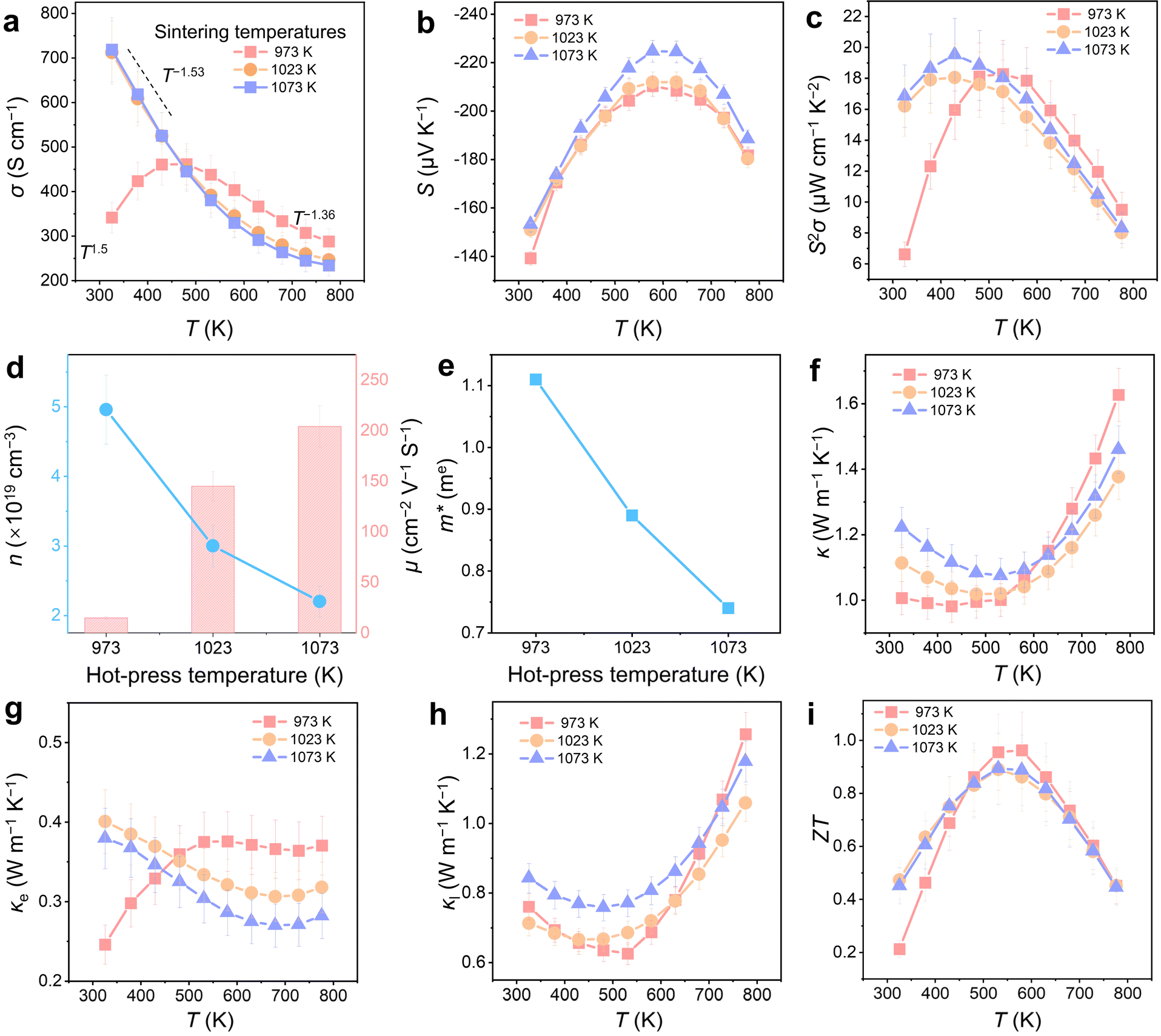 | ||
| Fig. 5 Thermoelectric performance of Mg3.4Bi1.29Sb0.7Te0.01, fabricated at different hot-press temperatures of 973, 1023, and 1073 K. Temperature-dependent (a) electrical conductivity (σ) and (b) Seebeck coefficient (S), and (c) S2σ. Room-temperature (d) carrier concentration (n) and mobility (μ) and (e) effective mass (m*). Temperature-dependent (f) κ, (g) electrical thermal conductivity (κe), (h) lattice thermal conductivity (κl), and (i) ZT. | ||
To understand the variations in electrical properties, Fig. 5d presents the room-temperature n and μ. As the sintering temperature increases, the room-temperature μ values of the samples sintered at 1023 K and 1073 K are significantly higher than that of the sample sintered at 973 K. For example, at room temperature, μ increases from 10 cm2 V−1 s−1 at 973 K to 145 cm2 V−1 s−1 at 1023 K and 204 cm2 V−1 s−1 at 1073 K. This improvement is primarily attributed to the reduction in grain boundary scattering for the carriers, despite a decrease in n due to the increase in VMg caused by the higher sintering temperatures. As shown in Fig. 5e, the increase in sintering temperature also results in a reduction in the effective mass (m*) of the carriers, as calculated using the single parabolic band (SPB) model.51 This is largely due to the decrease in n, further suggesting that no significant energy filtering effect is present. Consequently, with the improvement in μ, σ increases significantly, leading to a marked enhancement in S2σ.
Fig. 5f–h show the temperature-dependent κ, κe, and κl for the Mg3.4Bi1.29Sb0.7Te0.01 samples sintered at 973, 1023, and 1073 K, respectively. The κe was estimated using the Wiedemann–Franz law (κe = LσT), where L represents the Lorenz number estimated using the single parabolic band (SPB) model.52 As shown in Fig. 5g, the temperature-dependent κe increases, primarily due to the corresponding increase in σ. Fig. 5h illustrates that as the sintering temperature increases, the κl also shows a noticeable increase. This can be attributed to the increase in grain size, where the reduction in grain boundary intensity weakens phonon scattering. Additionally, a crossover is observed in the κl region beyond 632 K. This phenomenon can be attributed to the higher carrier concentration in the sample sintered at 973 K, which results in a more pronounced bipolar thermal effect, thereby increasing its κl. Overall, the increase in sintering temperature slightly increases the κ, as depicted in Fig. 5f. However, despite this increase in κ, the S2σ significantly improves, leading to a notable enhancement in the near-room-temperature ZT values for the samples sintered at 1023 K and 1073 K. Fig. 5i shows the temperature-dependent ZT values, with the ZT reaching 0.5 at room temperature, an improvement of 238%. The peak ZT remains high at 531 K, approaching a value of 0.9. Meanwhile, the samples have demonstrated excellent thermal cycling stability, showing no significant changes in performance after 20 cycles of testing. Regarding chemical stability, the samples exhibit relative stability in air but show sensitivity to water, as detailed in Fig. S7–S10 in the ESI.†
Conclusion
This study utilized a two-step method to progressively enhance the thermoelectric performance of Mg3Bi2-based materials over a broad temperature range near room temperature. First, by adjusting the excess Mg content, we achieved a transition from p-type to n-type conduction while optimizing n and μ, leading to a significant increase in ZT, with a peak ZT value of ∼1 at 573 K. In the second step, we fine-tuned the sintering temperature during the high-temperature sintering process, engineering a microstructure that increased grain size without altering the system's composition. This further improved electron mobility near room temperature. Consequently, the ZT value at 323 K rose from 0.2 to nearly 0.5, with a peak ZT close to 0.9 at 500 K. This work provides valuable insights for optimizing the preparation of Mg3Bi2-based materials and serves as a useful reference for future improvement strategies.Data availability
The data supporting this article have been included as part of the ESI.†Conflicts of interest
There are no conflicts to declare.Acknowledgements
This work was financially supported by the Foundation of Shaanxi University of Science & Technology (Grant No. 2017GBJ-03). The authors are thankful for the financial support from the Australian Research Council, and QUT Capacity Building Professor Program, and acknowledge the National Computational Infrastructure, supported by the Australian government, for providing computational resources and service. This work was enabled by the use of the Central Analytical Research Facility hosted by the Institute for Future Environments at QUT. The authors acknowledge the support from the Xi'an International Science and Technology Cooperation Base of Semiconductor Thermoelectric Materials and Devices.References
- J. He and T. M. Tritt, Science, 2017, 357, eaak9997 Search PubMed.
- Y. Xiao and L.-D. Zhao, Science, 2020, 367, 1196–1197 CrossRef CAS PubMed.
- Q. Yang, S. Yang, P. Qiu, L. Peng, T.-R. Wei, Z. Zhang, X. Shi and L. Chen, Science, 2022, 377, 854–858 CrossRef CAS PubMed.
- B. Jiang, Y. Yu, J. Cui, X. Liu, L. Xie, J. Liao, Q. Zhang, Y. Huang, S. Ning, B. Jia, B. Zhu, S. Bai, L. Chen, J. Pennycook Stephen and J. He, Science, 2021, 371, 830–834 CrossRef CAS PubMed.
- W. Chen, X.-L. Shi, M. Li, T. Liu, Y. Mao, Q. Liu, M. Dargusch, J. Zou, G. Q. M. Lu and Z.-G. Chen, Science, 2024, 386, 1265–1271 CrossRef CAS PubMed.
- T.-R. Wei, P. Qiu, K. Zhao, X. Shi and L. Chen, Adv. Mater., 2023, 35, 2110236 CrossRef CAS PubMed.
- Q.-X. Hu, W.-D. Liu, L. Zhang, H. Gao, D.-Z. Wang, T. Wu, X.-L. Shi, M. Li, Q.-F. Liu, Y.-L. Yang and Z.-G. Chen, Adv. Energy Mater., 2024, 14, 2401890 CrossRef CAS.
- M. Rakshit, D. Jana and D. Banerjee, J. Mater. Chem. A, 2022, 10, 6872–6926 RSC.
- J. Sun, Y. Zhang, Y. Fan, X. Tang and G. Tan, Chem. Eng. J., 2022, 431, 133699 CrossRef CAS.
- X. Zhang, Z. Bu, S. Lin, Z. Chen, W. Li and Y. Pei, Joule, 2020, 4, 986–1003 CrossRef CAS.
- H. Lai, Y. Peng, M. Wang, R. Shi, J. Chen, C. Liu, Y. Wang, L. Miao and H. Wei, J. Adv. Ceram., 2023, 12, 228–241 CrossRef CAS.
- G. Rogl and P. F. Rogl, Crystals, 2023, 13, 1152 CrossRef CAS.
- X.-L. Shi, J. Zou and Z.-G. Chen, Chem. Rev., 2020, 120, 7399–7515 CrossRef CAS PubMed.
- Z. Zhou, G. Han, X. Lu, G. Wang and X. Zhou, J. Magnesium Alloys, 2022, 10, 1719–1736 CAS.
- X. Chen, H. Wu, J. Cui, Y. Xiao, Y. Zhang, J. He, Y. Chen, J. Cao, W. Cai, S. J. Pennycook, Z. Liu, L.-D. Zhao and J. Sui, Nano Energy, 2018, 52, 246–255 CAS.
- L. Wu, Z. Zhou, G. Han, B. Zhang, J. Yu, H. Wang, Y. Chen, X. Lu, G. Wang and X. Zhou, Chem. Eng. J., 2023, 475, 145988 CAS.
- K. Imasato, M. Wood, S. Anand, J. J. Kuo and G. J. Snyder, Adv. Energy Sustainability Res., 2022, 3, 2100208 CAS.
- H. Tamaki, H. K. Sato and T. Kanno, Adv. Mater., 2016, 28, 10182–10187 CAS.
- K. Imasato, S. Ohno, S. D. Kang and G. J. Snyder, APL Mater., 2018, 6, 016106 Search PubMed.
- P. Ying, L. Wilkens, H. Reith, N. P. Rodriguez, X. Hong, Q. Lu, C. Hess, K. Nielsch and R. He, Energy Environ. Sci., 2022, 15, 2557–2566 CAS.
- J.-W. Li, Z. Han, J. Yu, H.-L. Zhuang, H. Hu, B. Su, H. Li, Y. Jiang, L. Chen, W. Liu, Q. Zheng and J.-F. Li, Nat. Commun., 2023, 14, 7428 Search PubMed.
- L. Wang, W. Zhang, S. Y. Back, N. Kawamoto, D. H. Nguyen and T. Mori, Nat. Commun., 2024, 15, 6800 CAS.
- X. Shi, X. Zhang, A. Ganose, J. Park, C. Sun, Z. Chen, S. Lin, W. Li, A. Jain and Y. Pei, Mater. Today Phys., 2021, 18, 100362 CAS.
- K. Imasato, S. D. Kang, S. Ohno and G. J. Snyder, Mater. Horiz., 2018, 5, 59–64 CAS.
- M. Wood, J. J. Kuo, K. Imasato and G. J. Snyder, Adv. Mater., 2019, 31, 1902337 Search PubMed.
- T. Luo, J. J. Kuo, K. J. Griffith, K. Imasato, O. Cojocaru-Mirédin, M. Wuttig, B. Gault, Y. Yu and G. J. Snyder, Adv. Funct. Mater., 2021, 31, 2100258 CAS.
- Z. Liang, C. Xu, H. Shang, M. Ning, T. Tong, S. Song, W. Ren, X. Shi, X. Liu, F. Ding, J. Bao, D. Wang and Z. Ren, Adv. Energy Mater., 2023, 13, 2301107 CAS.
- J. Lei, K. Zhao, J. Liao, S. Yang, Z. Zhang, T.-R. Wei, P. Qiu, M. Zhu, L. Chen and X. Shi, Nat. Commun., 2024, 15, 6588 CAS.
- J. Zhang, L. Song, K. A. Borup, M. R. V. Jørgensen and B. B. Iversen, Adv. Energy Mater., 2018, 8, 1702776 Search PubMed.
- X. Mo, J. Liao, G. Yuan, S. Zhu, X. Lei, L. Huang, Q. Zhang, C. Wang and Z. Ren, J. Magnesium Alloys, 2022, 10, 1024–1032 CAS.
- X. Shi, T. Zhao, X. Zhang, C. Sun, Z. Chen, S. Lin, W. Li, H. Gu and Y. Pei, Adv. Mater., 2019, 31, 1903387 Search PubMed.
- J. Zhang, L. Song and B. B. Iversen, Angew. Chem., Int. Ed., 2020, 59, 4278–4282 CrossRef CAS PubMed.
- K. Imasato, M. Wood, J. J. Kuo and G. J. Snyder, J. Mater. Chem. A, 2018, 6, 19941–19946 RSC.
- J. Zhang, L. Song and B. B. Iversen, Adv. Sci., 2020, 7, 2002867 CrossRef CAS PubMed.
- T. Kanno, H. Tamaki, H. K. Sato, S. D. Kang, S. Ohno, K. Imasato, J. J. Kuo, G. J. Snyder and Y. Miyazaki, Appl. Phys. Lett., 2018, 112, 033903 CrossRef.
- S. Chen, J. Wei, Z. Kang, X. Miao, D. An, W. Fan and C. Dun, Chem. Eng. J., 2024, 490, 151404 CrossRef CAS.
- K. Imasato, S. D. Kang and G. J. Snyder, Energy Environ. Sci., 2019, 12, 965–971 RSC.
- J. Mao, H. Zhu, Z. Ding, Z. Liu, G. A. Gamage, G. Chen and Z. Ren, Science, 2019, 365, 495–498 CAS.
- Z. Liang, C. Xu, H. Shang, Q. Zhu, F. Ding, J. Mao and Z. Ren, Mater. Today Phys., 2021, 19, 100413 CAS.
- Z. Liu, W. Gao, H. Oshima, K. Nagase, C.-H. Lee and T. Mori, Nat. Commun., 2022, 13, 1120 CAS.
- N. Qu, Y. Zhu, J. Zhu, K. Yu, F. Guo, Z. Liu, Q. Zhang, W. Cai and J. Sui, J. Magnesium Alloys, 2024, 12, 4538–4546 CrossRef CAS.
- H. Cho, S. Y. Back, N. Sato, Z. Liu, W. Gao, L. Wang, H. D. Nguyen, N. Kawamoto and T. Mori, Adv. Funct. Mater., 2024, 34, 2407017 CAS.
- X. Li, C. Sun, K. Yang, D. Liang, X. Ye, W. Song, W. Xu, W. Zhao and Q. Zhang, Small, 2024, 20, 2311478 CAS.
- K. Yang, X. Li, C. Sun, W. Song, W. Zhao and Q. Zhang, Adv. Funct. Mater., 2024, 34, 2315886 CAS.
- L. Yin, C. Chen, F. Zhang, X. Li, F. Bai, Z. Zhang, X. Wang, J. Mao, F. Cao, X. Chen, J. Sui, X. Liu and Q. Zhang, Acta Mater., 2020, 198, 25–34 CAS.
- M. Ozen, M. Yahyaoglu, C. Candolfi, I. Veremchuk, F. Kaiser, U. Burkhardt, G. J. Snyder, Y. Grin and U. Aydemir, J. Mater. Chem. A, 2021, 9, 1733–1742 RSC.
- C. Xu, M. Jian, Z. Liang, B.-H. Lei, S. Song, F. Zhang, D. J. Singh, Z. Feng and Z. Ren, Nano Energy, 2023, 106, 108036 CrossRef CAS.
- J.-S. Liang, X.-L. Shi, Y. Peng, W.-D. Liu, H.-Q. Yang, C.-Y. Liu, J.-L. Chen, Q. Zhou, L. Miao and Z.-G. Chen, Adv. Energy Mater., 2022, 12, 2201086 CrossRef CAS.
- S. Ohno, K. Imasato, S. Anand, H. Tamaki, S. D. Kang, P. Gorai, H. K. Sato, E. S. Toberer, T. Kanno and G. J. Snyder, Joule, 2018, 2, 141–154 CrossRef CAS.
- J. J. Kuo, S. D. Kang, K. Imasato, H. Tamaki, S. Ohno, T. Kanno and G. J. Snyder, Energy Environ. Sci., 2018, 11, 429–434 RSC.
- J. Zhu, X. Zhang, M. Guo, J. Li, J. Hu, S. Cai, W. Cai, Y. Zhang and J. Sui, Npj Comput. Mater., 2021, 7, 116 CrossRef CAS.
- H.-S. Kim, Z. M. Gibbs, Y. Tang, H. Wang and G. J. Snyder, APL Mater., 2015, 3, 041506 CrossRef.
Footnotes |
| † Electronic supplementary information (ESI) available. See DOI: https://doi.org/10.1039/d4ta08026b |
| ‡ These two authors contribute equally. |
| This journal is © The Royal Society of Chemistry 2025 |