
 Open Access Article
 This Open Access Article is licensed under a Creative Commons Attribution-Non Commercial 3.0 Unported Licence
Twin spacing manipulation of (111)-oriented nanotwinned copper via aeration flow control in a high-speed direct-current electroplating system with thiol organic additives
Hsiang-Sheng
Wei†
,
Kuan-Ling
Liu†
,
Hsu
Tsou
,
Hao-Yu
Ku
and
Chi-Chang
Hu
 *
*
Department of Chemical Engineering, National Tsing Hua University, Hsin-Chu, 300044, Taiwan. E-mail: cchu@che.nthu.edu.tw
First published on 11th January 2025
Abstract
It is a challenge to develop a cost-effective and time-efficient process for manufacturing nanotwinned copper foil with the precise control of twin spacing, a crucial determinant of nanotwinned copper properties. In this work, we modify the aeration flow rate near the cathode to adjust the mass transfer effects of chloride ions and 3-mercapto-1-propanesulfonate (MPS) in an acidic CuSO4 system. These modifications can change the copper crystallization and morphology of copper deposits, promoting the twin boundary formation. In particular, at a high plating current density of 40 A dm−2 and 10 °C in a direct current (dc) mode, the twin lamella distribution in the copper deposit with the twin spacing centered at ca. 136 nm can be simply narrowed down to 61 nm by increasing the aeration flow rate from 0.5 to 2.5 L min−1. The microstructures of copper foil have been examined using X-ray diffraction (XRD), scanning electron microscopy (SEM), transmission electron microscopy (TEM), ion-channeling images, an alpha-step profiler, atomic force microscopy (AFM), and electron backscatter diffraction (EBSD).
1. Introduction
Copper, with its superior electrical conductivity, affordability, malleability, and surface stability, remains a critical material across multiple domains. It has been extensively utilized in pillar bumping, under-bump metallization, redistribution layers, and through-silicon vias within the integrated circuit packaging, as well as the current collector for the negative electrode in lithium-ion and lithium-metal batteries (LIBs/LMBs).1,2However, the ongoing trend of semiconductor component shrinkage, driven by the demand for high chip performance, has led to concerns over the mechanical strength, electromigration resistance, and thermal stability of copper. In parallel, the quest for enhanced energy density in LIBs and LMBs necessitates the development of thinner current collectors that maintain sufficient mechanical integrity. As such, devising an efficient copper fabrication process capable of meeting these stringent requirements has emerged as a significant challenge in the copper electroplating industry. Among the various approaches explored, the introduction of nanotwins in copper is considered a highly promising method in altering the microstructures due to the superior properties it confers. For example, the (111)-nanotwinned copper has been found to exhibit extremely high mechanical strength without compromising the electrical conductivity compared to the coarse-grained copper,3 positioning it as a potential substrate in the advanced electronic and semiconductor industries, and the current collector of the negative electrode in LIBs/LMBs.
The (111)-nanotwinned copper stands out for its ability to reconcile the typical tradeoff between mechanical strength and conductivity, boasting an ultrahigh tensile strength of approximately 1 GPa.3–5 In the context of electromigration resistance, the (1110)-nanotwinned structure notably restricts atomic diffusion relative to conventional polycrystalline copper, thereby ensuring enhanced stability under high-current conditions.6 In addition, nanotwinned copper has been reported to exhibit exceptional thermal stability, retaining its properties even after annealing at temperatures as high as 800 °C.7
Given the established superiority of (111)-nanotwinned copper in terms of mechanical, electrical, and thermal properties, the current challenge lies in identifying the most effective method for its production. Several techniques can induce the formation of nanotwins in copper, including dynamic plastic deformation,8 phase transformation,3 annealing,9 magnetron sputtering,10 and electroplating. Among these, electroplating is the most widely used due to its cost-effectiveness, time efficiency, and ease of control.
The strategies for inducing the growth of nanotwins in copper electroplating can be broadly categorized into the thermodynamic and crystallographic perspectives. From a thermodynamic viewpoint, being commonly described in the pulse electrodeposition (PED) mode, during the time-off period, the accumulated stress in the deposit manufactured at high rates during the time-on period can be released through the recrystallization of copper grains (stress relaxation process) to form the nanotwinned structure. This phenomenon was confirmed by the evidence of in situ residual stress measurements.11,12 From a crystallographic viewpoint, the crystalline structure can be controlled by the electroplating overpotential or the ratio of average current to cupric ions. According to the Winand diagram, nucleation of (220) crystal-oriented twin copper and (111) crystal-oriented twin copper probably occurs when the crystalline structure is controlled in the basis-oriented reproduction (BR) and field-oriented texture (FT) types, respectively.13
Note that variations in the manufacturing processes generally affect the properties of nanotwinned copper, such as distinct crystal orientations, nanotwin densities, and especially average twin spacings. However, the control of average twin spacing in nanotwinned copper is limited although how to control the crystal orientation and nanotwin density has been extensively investigated in the literature. Recently, the reduction in the duty ratio (γ, defined as the time ratio between time-on and whole pulse cycle) and the increase in the pulse frequency (f) in the pulse electroplating deposition (PED) mode could be used to reduce the twin spacings.14,15 However, the control of twin spacing in the dc plating mode remains insufficient, particularly considering that the future Cu pillar plating processes for wafer packaging are anticipated to employ current densities up to 400 mA cm−2 (i.e., 40 A dm−2, 40 ASD) in the dc mode. Furthermore, variations in average twin spacing are believed to significantly influence the properties of nanotwinned copper. From a thermodynamic perspective, altering twin spacing modifies the atomic step density on copper surfaces, where atomic steps serve as ideal active sites for many reactions, such as Kirkendall void formation during oxidation reactions.16 Moreover, in the context of zero excess lithium metal batteries, the variation in atomic step density on (111)-oriented copper foil surfaces has a profound impact on the battery performance.17 Some studies also have demonstrated that changes in twin spacings could result in variation in ultimate tensile strength, fracture elongation, and chemical corrosion resistance.15,18 Therefore, optimizing the dc plating parameters to regulate the twin spacings within copper at high plating rates is considered a critical step forward in advancing the future industrial applications.
Our previous work19 demonstrated that copper foil with a highly textured (111)-oriented nanotwinned structure, featuring an average twin spacing of ca. 105 nm, could be prepared at 40 ASD in the dc mode from an optimized plating bath containing 1.08 M CuSO4 and 3 vol% H2SO4 (considering the saturation solubility of cupric ions and ionic conductivity for high-rate copper deposition) with additives of 40 ppm chloride ions and 300 ppm 3-mercapto-1-propanesulfonate (MPS) at 10 °C under controlled forced convection. Here, MPS, a simple organic molecule, is composed of the thiol group at one end and the sulfonate group at another end. The thiol group has been found to bond strongly with electroplated copper due to its high affinity to copper atoms.20 The sulfonate group was reported to exhibit an acceleration effect by improving the rate determining step of the regular two-step copper reduction deposition through a novel reaction routine via the formation of thiol-chloride-Cu+ intermediates.21 The relatively concentrated thiol-chloride-Cu+ intermediates at the cathode surface facilitate the high-density nucleation of metallic copper and promote the formation of copper nanotwins, which commonly evolves a thermodynamically favorable microstructure with large columnar grains and dense twin boundaries.19 Since the semiconductor packaging needs copper pillars of 200 μm, which require a current density of 40 ASD to achieve an acceptable throughput,22 how to ensure the electro-crystallization of copper plating in the field-oriented texture type is a challenge.
According to the Winand diagram,13 modifying the inhibition intensity (additive activity) and mass transfer characteristics of cupric ions can significantly influence the electrocrystallization mode of the copper lattice. This model defines two stable types for manufacturing nanotwinned copper: one for the (220)-oriented nanotwinned copper lattices, associated with the basis reproduction type (BR type), and another for the (111)-oriented nanotwinned copper lattices, linked to the field-oriented texture type (FT type). Here, a simple but effective approach, i.e., gas agitation to create forced convection near the electrode surfaces, is proposed to promote the diffusion-limited current density for the transformation in the electrocrystallization mode from the unoriented dispersion type toward the field-oriented texture type. Moreover, the change in the aeration flow rate commonly alters the activity of convection-sensitive additives, e.g., MPS. Thus, in this work, this factor is further utilized to regulate the average twin spacing of (111)-oriented nanotwinned copper deposits between 61 nm and 136 nm at an electroplating rate of 400 mA cm−2, which is sufficiently high for commercial utilization. Additionally, the electrochemical analysis could enhance our understanding on the nanotwin formation mechanism in copper and sheds light on the relationship between mass transfer dynamics and additive effects.
2. Experimental
2.1. Copper foil preparation
A Haring cell with a parallel arrangement of the anode and cathode was utilized. The anode, a dimensionally stable anode (DSA®) with a long mesh structure, consisted of 55 wt% tantalum oxide and 30 wt% iridium oxides. The cathode was a pure titanium plate, meticulously polished to a glossy, uniform finish. The polishing process progressed sequentially from 400 grit to 1200, 2500, and finally, 4000 grit sandpaper. The bath temperature was precisely maintained at 10 ± 0.2 °C using a U-shaped glass tube connected to a water thermostat. Gas agitation driven by an air pump was employed to induce forced convection on both sides of the electrode. The upper and lower limits of the reliable flow rates, 2.5 L·min−1 and 0.5 L·min−1, were utilized to adjust the inhibition intensity of MPS to amplify the difference in the electro-crystallization mode to prove the concept in controlling the average twin spacing of (111)-oriented nanotwinned copper deposits. The schematic of the copper electroplating apparatus is shown in Fig. 1.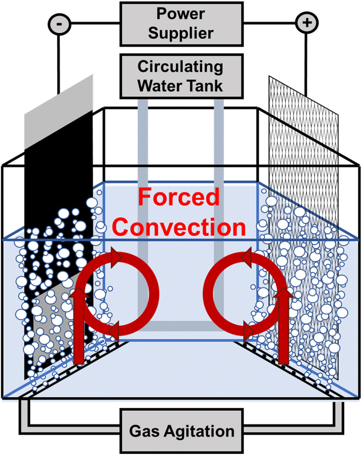 | ||
| Fig. 1 The schematic of the copper electroplating apparatus. | ||
Copper foil was electroplated onto the pretreated titanium plate in the dc mode using a rectifier (B&K Precision 9173B) at a current density of 400 mA·cm−2 for 5 min. The virginal makeup solution (VMS) comprised 1.08 M copper sulfonate and 3 vol% sulfonic acid (the optimized composition considering the saturation solubility of cupric ions and ionic conductivity). Before electroplating, 40 ppm chloride ions (NaCl, Showa Chemical, 99%) and 300 ppm MPS were added to the VMS. Deionized water (18.2 MΩ cm) from a Millipore system was used to ensure minimal impurities in the electroplating bath. After electroplating, the copper foil was examined using various analytical techniques.
2.2. Materials characterization
The surface morphology of copper foil was examined using a scanning electron microscope (SEM, Hitachi SU-8010), a scanning probe microscope (SPM, Bruker Dimension ICON), and an alpha-step profiler (Veeco, Dektak 150). A high-resolution field emission scanning electron microscope (HRFESEM, JEOL JSM-7800F) was employed for the detailed analysis of grain size, size distribution, and crystal structure. X-ray diffraction (XRD, Bruker D8A25) patterns were utilized to determine the crystal orientations. Ion-channeling images, obtained after milling with a focused ion beam (FIB, TESCAN GAIA3), were used to investigate the cross-sectional microstructures. The quantification of twin lamella distribution requires milling copper foil using the FIB technique to create thin sections. These sections are mounted on a TEM copper grid to carefully examine the microstructure. The sheet resistance of copper foil was measured using a four-point probe resistance meter (Quatek, QTI-5601TSR).2.3. Electrochemical analysis
The rotating ring-disk electrode (RRDE-3A, ALS Co., Ltd.) at two rotating speeds, 1000 rpm and 3000 rpm, was utilized to study the electrochemical kinetics of copper plating in VMS containing 40 ppm chloride ions and 300 ppm MPS. The system consisted of a glassy carbon working electrode, a platinum ring electrode, a metallic mesh counter electrode, and a Hg/Hg2SO4 reference electrode immersed in 100 ml of the electrolyte. Linear sweep voltammetry (LSV) and chronopotentiometry (CP) were employed to obtain critical insights into the electrochemical behavior of cupric ions, chloride ions, and MPS.3. Results and discussion
3.1. Modification guidelines of (111)-oriented nanotwinned copper
According to the Winand diagram,13 the mass transfer characteristics of cupric ions are adjusted by varying the aeration flow rate at the cathode surface from 0.5 L·min−1 to 2.5 L·min−1 to alter the adsorption performance of chloride ions and twin-inducing additives (e.g., MPS), probably changing the electrocrystallization mode within the FT type. The 2.5 L·min−1 case composes a lower overpotential because of the higher transport rate of MPS, leading to higher adsorption and coverage of MPS. Consequently, the copper lattice can provide larger capacity to tolerate the slight increase in the excess energy within the copper lattice, favorable to the nanotwinned structure formation. In other words, the copper lattice can be composed of more nanotwins when the aeration flow rate is increased from 0.5 L to 2.5 L·min−1.Here the nanotwinned copper with two twin distributions can be classified according to the Winand diagram. The smaller average twin spacing is, the closer to the BR type front in the electrocrystallization mode of the FT type is Table 1 lists the two twin-inducing conditions near the cathodes.
| Condition | 0.5 L min−1 300 ppm MPS | 2.5 L min−1 300 ppm MPS | Detailed section |
|---|---|---|---|
| MPS activity | Less active | More active | 3.2 |
| Electrocrystallization mode | FT type (close to UD type) | FT type (close to BR type) | 3.2 |
| Crystal orientation | (111) | (111) | 3.3 |
| Grain size | ∼600 nm | ∼600 nm | 3.3 |
| Roughness | Lower | Higher | 3.4 |
| Average twin spacing | 136.0 nm | 61.37 nm | 3.5 |
| Conductivity | Lower | Higher | 3.6 |
3.2. Convection-sensitive properties of Cl− and MPS in the electroplating system
According to the literature,23 the adsorption of MPS on the cathode is convection-sensitive, confirmed by the more potential sensitive at higher rotating rates of the RRDE when adding MPS. This phenomenon has been attributed to the rapid desorption and re-adsorption kinetics of MPS.24 If the mass transfer conditions near the cathode in the electroplating bath are improved, the desorption/re-adsorption rates of MPS may be further improved. This allows the desorbed, unreacted MPS to have a higher likelihood of re-adsorption onto the cathode surface compared to the case of poor mass transfer conditions. The efficient re-adsorption can alleviate the movement of MPS to the anode, reducing the further oxidation reactions between MPS and bulk Cu2+ that would lead to the formation of bis-(sodium sulfopropyl)-disulfide (SPS). Such an oxidation product may contribute to an additional route for the accelerator effect and causes the aging issue of additives by the formation of 1,3-propane disulfonic acid (DPS) which could not participate in the catalytic electroplating.25To further understand the behavior of MPS, linear sweep voltammetry (LSV) was conducted using a rotating ring-disk electrode (RRDE) system from 0 mV to −1000 mV (vs. Hg/Hg2SO4) at 5 mV·s−1. The typical results shown in Fig. 2(a) and (b) can be divided into two distinct regions for discussion: the Cu+-rich region (from −250 mV to −600 mV) and the Cu+-stable region (from −600 mV to −1000 mV). Note that the reduction of Cu2+ to Cu(0) can be described using two key reactions.26–28
| Cu2+ + e → Cu+ E0 = +0.16 V vs. SHE | (1) |
| Cu+ + e → Cu E0 = +0.52 V vs. SHE | (2) |
 | ||
| Fig. 2 (a and b) The RRDE study for (a) the LSVs of the disk electrode and (b) the enlarged curves of (a) from −300 mV to −400 mV and (c) the corresponding ring current against the disk electrode potential. (d) The chronopotentiograms measured at 18 mA·cm−2 with chloride ions and MPS addition. | ||
In the Cu+-rich region, the reduction rate of Cu+ on the disk at the second step (reaction (2)) is relatively slower than the rate of Cu+ migration away from the disk. This difference allows Cu+ to be detected on the ring electrode. In contrast, in the Cu+-stable region, the reduction rate of Cu+ is significantly enhanced due to the more negative potentials, resulting in the depletion of Cu+ on the disk. Thus, the Cu+-stable region is critical for understanding the bulk deposition behavior of copper foil.
Fig. 2(a) illustrates the overlapping of LSV curves obtained on the disk electrode under two aeration flows, suggesting that the variation in the aeration flow does not significantly influence the second step of Cu2+ reduction or the overall deposition rate. Consequently, the primary effect of changing the aeration flow is concentrated on the first step of the cupric ion reduction process. Fig. 2(b), a magnified view of the Cu+-rich region (from −300 mV to −400 mV), demonstrates that the aeration flow rate substantially impacts the onset potential of the copper electroplating reaction. This suggests that the aeration flow rate can modulate the first step of cupric ion reduction, likely through enhanced adsorption of convection-sensitive MPS. Thus, the MPS–Cl− coordination complex, spectroscopically observed, is believed to provide a depolarizing effect on copper reduction.29Fig. 2(c) displays the ring current corresponding to the disk electrode potentials in the LSV test of Fig. 2(a). When the Cu2+ ions were started to be reduced, the Cu+ reduction rate (reaction (2)) is much slower than the rate of Cu+ migration away from the disk. Thus, large amounts of Cu+ ions have been transported to the ring surface, conducting the oxidation of Cu+ (i.e., Cu+ → Cu2+ + e). However, when the potentials were shifted negatively, the rate of reaction (2) becomes too fast compared to the migration rate of Cu+ produced by reaction (1). Thus, the amount of Cu+ ions reaching the ring electrode starts to decrease, leading to the rapid decrease in the ring oxidation current density. Consequently, there exists a peak on the ring signal from −300 mV to −600 mV. Note that the increase of oxidation current density at potentials more negative than −600 mV is attributable to the oxidation reaction of CuCl. Without reactions (1) and (2), there are still two additional reduction reactions if the electroplating solutions contain chloride ions:30,31
| Cu2+ + Cl− + e → CuCl E0 = +0.559 V vs. SHE | (3) |
| CuCl + e → Cu + Cl− E0 = +0.137 V vs. SHE | (4) |
It is worth noting that in this two-step reduction reaction, unlike reactions (1) and (2), the second step is the rate-determining step, indicating the existence of a more stable intermediate, CuCl, during the copper electroplating. Since the concentration of chloride ions in the electroplating solution is pretty low (40 ppm, much lower than the effective concentration, 1 M), the rates of reactions (3) and (4) are much lower than those of reactions (1) and (2). Back to Fig. 1(c), the increase of oxidation current density at potentials more negative than −600 mV is reasonably due to the rate of reaction (3) being enhanced, producing lots of CuCl which migrates to the ring surface. The CuCl adsorbed on the ring surface then conducts the oxidation reaction:31
| CuCl + Cl− → CuCl2 + e E0 = +0.936 V vs. SHE | (5) |
Because of the low chloride-ion concentration, the increase in current density due to the CuCl oxidation on the ring electrode is much lower than the oxidation peak resulting from the Cu+ intermediate. Since the rate of reaction (4) is slower than that of reaction (3), CuCl cannot be consumed violently, leading to the absence of a sharp decrease in the oxidation current density in Fig. 2(c), even when the potentials are near −1000 mV. Due to the low reactivity of reactions (3) and (4), the potential region from −300 mV to −600 mV refers to the main working potential window of reactions (1) and (2) while the potential region from −600 mV to −1000 mV refers to the main working potential window of reactions (3) and (4). In the potential range from −300 mV to −600 mV in Fig. 2(c), the higher oxidation peak at 3000 rpm indicates a stronger increase in the first step of cupric ion reduction than at 1000 rpm, consistent with the variations in disk current density observed in Fig. 2(b). Additionally, previous articles3,12,32 posited that an increased amount of adsorbed Cu+ intermediates on the cathode surface may alleviate the film stress and provide additional sites for the growth of twinned grains. Consequently, the higher oxidation peak of Cu+ intermediates is considered to be an indicator of the optimal conditions for the twin-induced growth. Therefore, this demonstrates the concept that in the presence of MPS additives, improving mass transfer favors the formation of nanotwinned structures.
Back to Fig. 2(a), the curve of 1000 rpm shows a slightly larger disk current density than the one of 3000 rpm. The reason is that the reduction rate of reaction (3) at 1000 rpm is faster than the one at 3000 rpm. This implies that the rotating rate may have a negative impact on reaction (3). This result can be further confirmed by the tendency of the oxidation current density curve of both rotating rates at potentials more negative than −600 mV in Fig. 2(c).
Further validation of the convection-sensitive nature of the chloride ions and MPS is obtained from the chronopotentiometric (CP) measurements. Fig. 2(d) shows the CP curves at a current density of 18 mA·cm−2 which is close to the boundary between the Cu+-rich region and Cu+-stable region. Because reactions (1)–(4) can occur in the actual electroplating bath for preparing copper foil, testing the depolarization effect of chloride ions and MPS in this potential region is more in line with the actual electroplating situation. When chloride ions or MPS are introduced into the electroplating bath, both species exhibit a depolarizing effect on the working electrode (disk electrode) surface. Several important observations arise from this figure. First, the 3000 rpm case displays a less negative nucleation overpotential and quasi-steady-state overpotential than the 1000 rpm case, suggesting that superior mass transfer enhances the copper crystal nucleation, growth, and coalescence. Second, at a higher rotation speed, chloride ions exhibit a lower depolarizing effect, indicating that increasing the rotation speed exhibits a negative effect on the depolarizing capability of chloride ions. From the literature,33–36 the adsorption state of chloride ions is well investigated using advanced surface analysis methods such as Auger spectroscopy, low-energy electron diffraction (LEED), scanning tunneling microscopy (STM), atomic force microscopy (AFM). The chloride ions have been concluded to be adsorbed on the copper surface to various extents, depending on the electrode potential. At lower overpotentials, chloride ions prefer to form an ordered single ad-layer on the copper surface, while at higher overpotentials, a disordered multiple ad-layer is formed. In Fig. 2(d), at 3000 rpm, the quasi-steady-state overpotential is more positive than the one obtained at 1000 rpm. This implies that the adsorption layer of chloride ions at 3000 rpm is more ordered and fewer than the case at 1000 rpm, indicating that the depolarization effect of chloride ions at 3000 rpm is worse than the latter one. Third, the depletion of depolarization effect of chloride ions at 3000 rpm is faster than that obtained at 1000 rpm. This is because more stable Cu+ intermediates can be produced at 3000 rpm at this current density or in this potential region, which can be confirmed in Fig. 2(a) and (c), indicating that more Cu+ may be transformed into CuCl:30,31
| Cu+ + Cl− → CuCl | (6) |
Since the electrochemical reaction rate is still lower compared to the chemical side reactions in this situation, the small amount of CuCl is believed to form a loosely structured passivation layer, causing small extent of polarization; consequently, the overpotential is increased. However, this effect diminishes at the practical electroplating current density, 40 ASD, because at this high current density, both chemical side reactions or electrochemical reactions for forming CuCl would cause the reduction reaction (4) to re-generate chloride ions and finish the copper deposition, and then eliminate the passivation layer. Fourth, MPS shows a more pronounced depolarizing effect at 3000 rpm than the case at 1000 rpm. The depolarization overpotential at 3000 rpm is approximately 34.6 mV, while at 1000 rpm, it is about 19.5 mV. This can be attributed to two factors. First, according to the literature,37 MPS and the other organic additives need to compete with chloride ions for the adsorption sites on the copper surface. The competitiveness of individual additives must be based on the current density, potential, the individual additive concentration, and also the synergy between additives. At the rotating speed of 3000 rpm, the chloride ad-layer is more ordered and a sub-monolayer can be formed on the copper surface. Thus, the chloride ions are less competitive than MPS for adsorption sites on the copper surface. Furthermore, the thiol group of MPS may make adsorption more easy and facilitate a lower-energy charge transfer reaction, leading to copper lattice formation. Second, MPS should experience fewer interactions with Cu2+ in the bulk solution, reducing the probability of SPS and DPS formation, thereby improving the MPS efficiency.
3.3. Crystal orientation and grain size of copper foil
Fig. 3(a) presents the diffraction peaks centered at 43.33°, 50.47°, and 73.57°, corresponding to the (111), (200), and (220) planes of the copper lattice, respectively.38 Besides, Fig. 3(c) and (d) represent the enlarged images respectively corresponding to the (200) and (220) planes for clear identification. The two sharp (i.e., low half width), high-intensity peaks suggest that the copper foil exhibits a strong preferential orientation along the (111) plane. To perform a more comprehensive analysis of the crystallographic orientation distribution, the texture coefficient (TC) is employed to be a quantitative measurement. The TC value is determined on the basis of the relative intensities of the (hkl) planes in the X-ray diffraction (XRD) patterns; here the calculation was estimated using the following formula reported in the literature, detailed in eqn (7).39–41 | (7) |
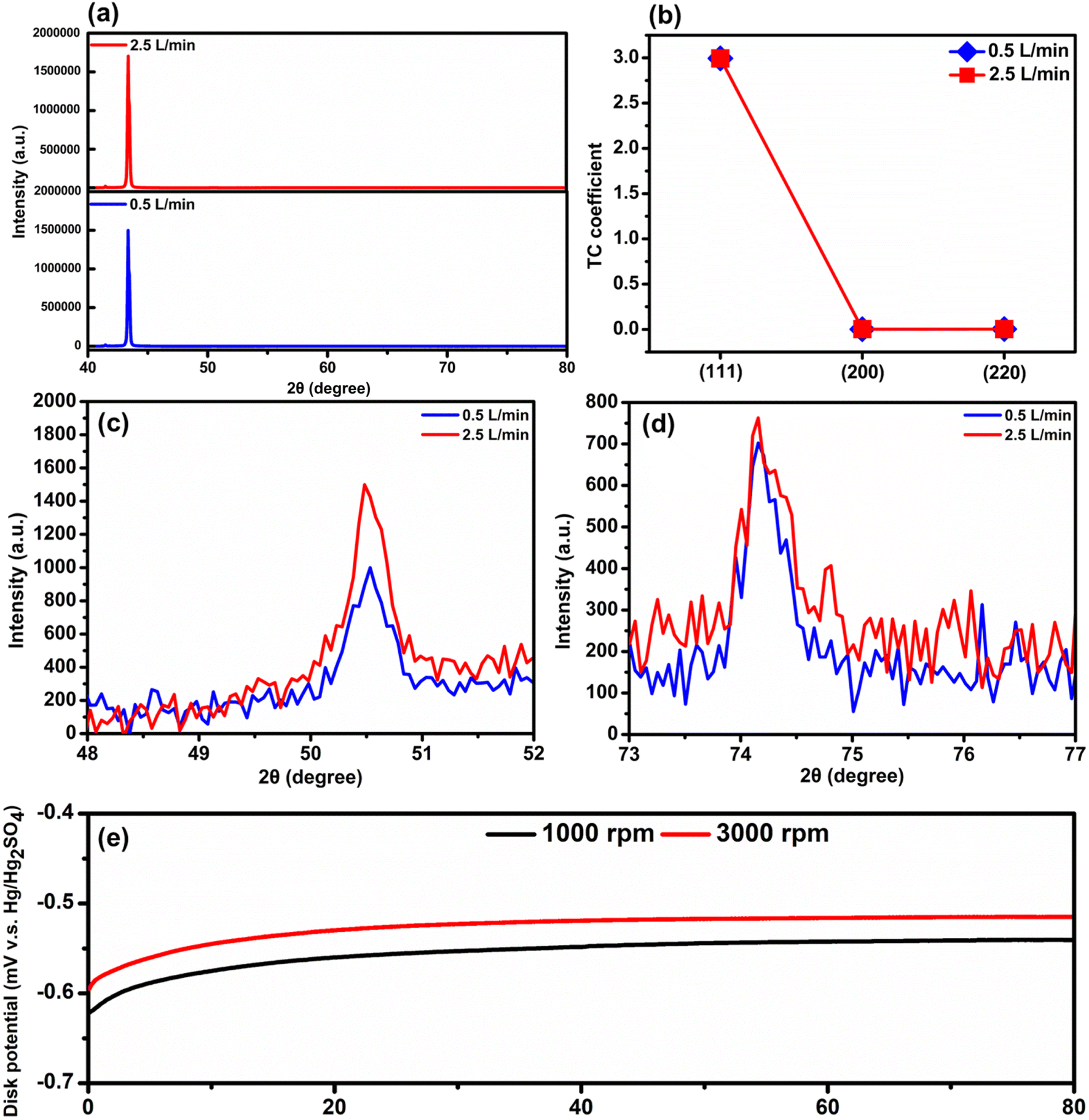 | ||
| Fig. 3 (a) The XRD patterns and (b) the texture coefficient values of Cu plated at 40 ASD at the aeration flow rates of 0.5 and 2.5 L·min−1 in the VMS added with 40 ppm chloride ions and 300 ppm MPS; the enlarged XRD images (c) from 48° to 52° and (d) from 73° to 77°. (e) The chronopotentiograms of disk electrodes at 1000 and 3000 rpm in the VMS added with 40 ppm chloride ions and 300 ppm MPS at 18 mA·cm−2. | ||
The relative peak intensity, I(hkl), corresponds to the (hkl) reflection of a copper deposit, while I0(hkl) denotes the intensity for a randomly oriented copper powder sample (JCPDS, Reference code: 00-004-0836). In this analysis, the reflection number n is set to 3. A higher texture coefficient (TC), nearing the theoretical maximum of 3, signifies a greater degree of preferential crystallographic orientation in the copper foil. As illustrated in Fig. 3(b), the TC values of Cu foil prepared at the aeration flow rates of 0.5 L·min−1 and 2.5 L·min−1 are equal to 2.995 and 2.993, respectively, indicating a strong (111) texture orientation with a negligible difference.
From the literature,42 the order of crystalline orientations with respect to increasing the nucleation overpotential is: η(111) < η(200) ≪ η(220), while with respect to increasing the activation overpotential of copper deposition is: η(220) < η(200) < η(111). When the nucleation reaction is suppressed, facets with high growth rates, such as the (110) plane, are expected to dominate, while in the absence of such suppression, the (111) plane is more likely to prevail; i.e., the Cu deposition preferred the 1-D nucleation when the nucleation reaction is suppressed. The 1-D nucleation copper lattice is the main electrocrystallization mode of the BR type. For the case without suppressing the nucleation, the copper lattice preferred the 2-D nucleation or 3-D nucleation, corresponding to the electrocrystallization mode of the FT type and UD type, respectively.
Note that the FT type corresponds to the (111)-oriented twin-induced condition. Thus, the results in Fig. 3(a–d) reveal that both cases consist of a very high textural (111)-oriented copper lattice, meaning that both cases are not the BR type electro-crystallization mode. Besides, the CP curves in Fig. 3(e) confirm that MPS enables to facilitate the nucleation from the reduced nucleation overpotential in the 3000 rpm case compared to the study measured at 1000 rpm, supporting this interpretation.
The XRD measurements are further corroborated by the EBSD images shown in Fig. 4(a) and (b) where the blue color on EBSD images represents (111)-orientation according to the inverse pole figure of copper, confirming that the copper foil exhibits a predominant (111) orientation under two aeration conditions. Additionally, Fig. 4(e) shows that the grain size distribution and average grain size of Cu prepared at 2.5 L·min−1 are slightly higher than those obtained at 0.5 L·min−1. However, the average grain size of both cases is around 600 nm, indicating the relative stability of the average grain size through the variation in the aeration flow. This consistency in grain size is significant for later material and electrical analyses.
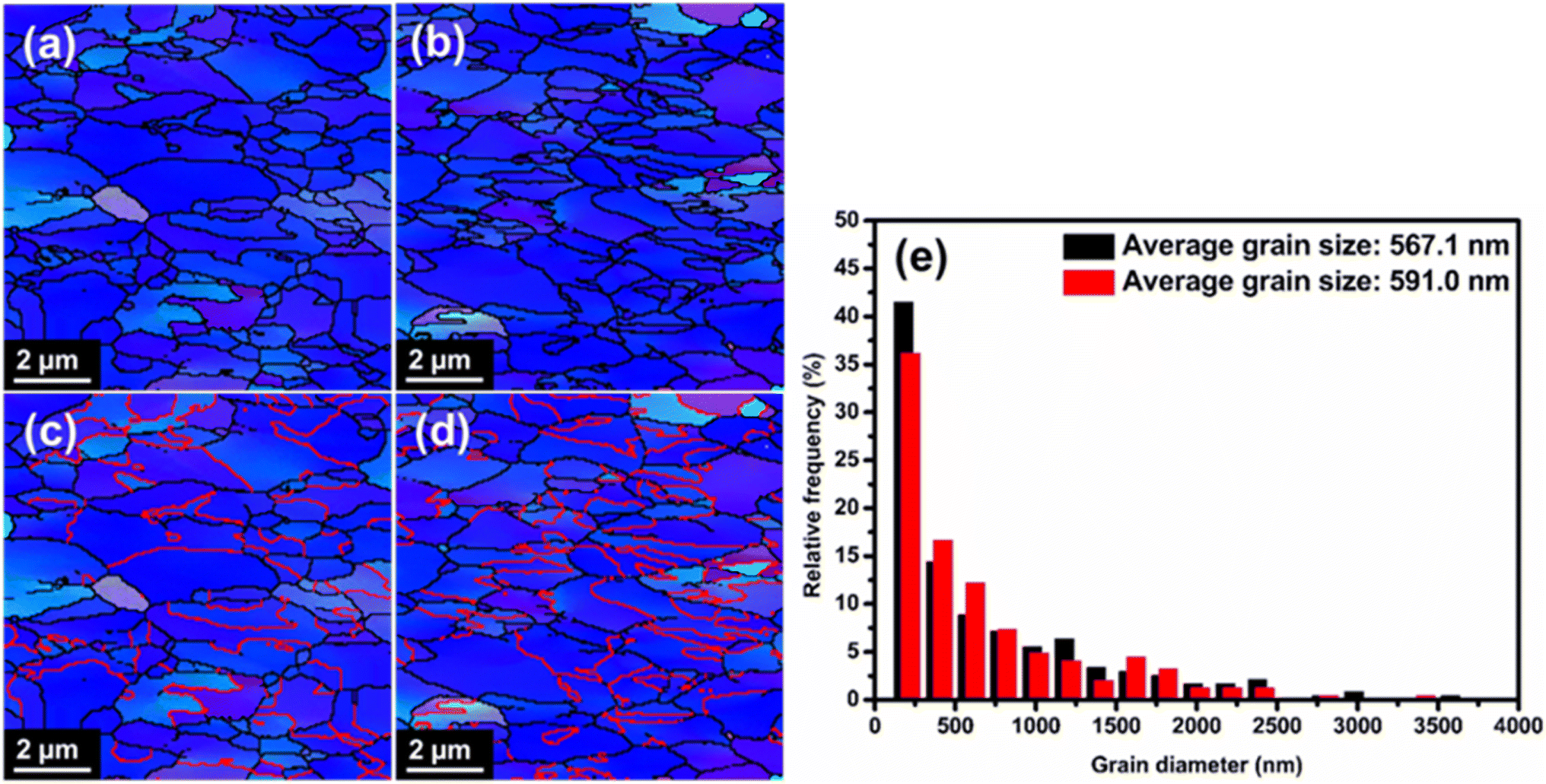 | ||
| Fig. 4 The EBSD images of copper foil prepared at the aeration flow rates of (a and c) 0.5 L·min−1 and (b and d) 2.5 L·min−1 with the red line marks of (111) nanotwin in (c and d). (e) The grain sizes of copper foil prepared at the aeration flow rates of 0.5 L·min−1 (black bar) and 2.5 L·min−1 (red bar). | ||
3.4. Morphology & roughness of copper foil
Fig. 5(a) presents the surface morphology of copper foil plated at two aeration flow rates. Both Cu foils exhibit transverse layered structures on the crystal surface, indicative of nanotwinned structures.43–46 The formation of these layers is attributed to a unique twin formation mechanism. As highlighted in the literature,43 the accumulation of high residual stress in copper triggers the stress relaxation processes to stabilize the lattice. Due to the low stacking fault energy, copper has a high propensity to form twin structures to reduce the residual stress through the stress relaxation process.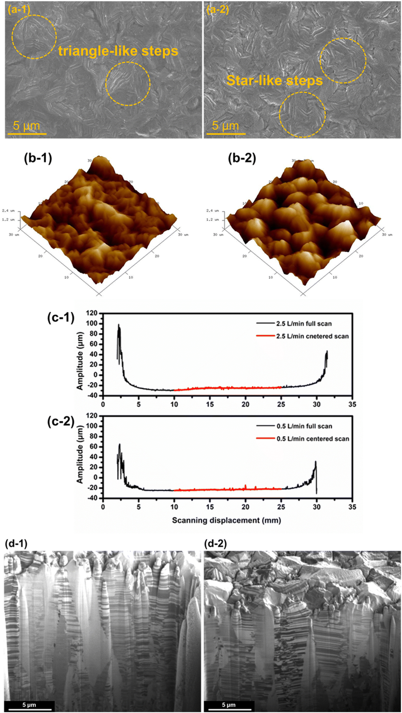 | ||
| Fig. 5 (a) SEM images, (b) AFM images, (c) the alpha step measurements, and (d) the ion-channeling images of the cross-section microstructure after the FIB milling of the Cu foil at an aeration flow rate of (1) 0.5 L·min−1 and (2) 2.5 L·min−1. | ||
In detail, the twinning process initiates at the triple junctions of grain boundaries, where the local residual stress is concentrated. Then, the twin lamellae with favorable orientations grow and reach neighboring grain boundaries to form twin terraces. The periodic growth of these terraces results in a high density of nanotwins within the grains, that is the transverse layers on the copper lattice, which can be observed in Fig. 5(a). Furthermore, the Cu foil plated at an aeration flow rate of 0.5 L·min−1 results in a triangular step structure, while the product made at an aeration flow rate of 2.5 L·min−1 exhibits star-like steps. According to the literature,15 the morphology of nanotwinned copper is influenced by the change in the twin-inducing process. Thus, the above phenomenon is reasonably attributed to the coverage difference in chloride ions and MPS adsorption, which plays a crucial role in twin formation in this electroplating system.
Fig. 5(b) illustrates the AFM analysis of copper foil (in the center regions) prepared at two aeration flow rates for gaining a deep understanding on the roughness of copper foil. In Fig. 5(b-1), the relatively weak forced convection (i.e., 0.5 L·min−1) leads to an uneven distribution of cupric ions, resulting in larger variations in protrusion size compared to the more uniform and larger protrusions found in the high-convection case (i.e., 2.5 L·min−1) in Fig. 5(b-2). The strong convection can promote the MPS adsorption and its depolarization effect. Also, MPS can enhance the nucleation process to favor the formation of a (111)-oriented copper lattice. Thus, the copper foil plated at the aeration flow rate of 2.5 L·min−1 consists of larger protrusions in comparison with the case at 0.5 L·min−1, aligning with the results from EBSD measurements. The surface roughness in the 2.5 L·min−1 case, indicated by the Ra value (from eqn (8)), Rq value (from eqn (9)), and the projected surface area in Table 2, is also higher than that in the 0.5 L·min−1 case:
 | (8) |
 | (9) |
| Condition | R a (nm) | R q (nm) | Surface area (μm2) | Projected surface area (μm2) |
|---|---|---|---|---|
| 0.5 L·min−1 300 ppm MPS | 205 | 259 | 965 | 900 |
| 2.5 L·min−1 300 ppm MPS | 282 | 352 | 984 | 900 |
For the surface topography of copper foil on a large scale, the findings are displayed in Fig. 5(c). The specimen processed with an aeration flow rate of 2.5 L·min−1 exhibited a uniform distribution of protrusions, while the sample prepared at 0.5 L·min−1 displayed random and distinct high peaks and low valleys. The Ra and Rq values, detailed in Table 3, are consistent with the corresponding AFM measurements, reinforcing the validity of the observed surface features.
| Condition | R a (nm) | R q (nm) |
|---|---|---|
| 0.5 L·min−1 300 ppm MPS | 351.7 | 820.0 |
| 2.5 L·min−1 300 ppm MPS | 632.6 | 982.3 |
3.5. Qualitative & quantitative analyses of the nanotwinned structure
The staggered arrangement of twin lamellae and matrices in the nanotwinned copper foil results in a distinct material contrast observable in the cross-sectional images acquired through the focused ion beam (FIB) microscope. This contrast forms a striped pattern that confirms the presence of a nanotwinned (111) orientation structure, as shown in Fig. 5(d). Under the poor twin formation conditions, as found in Fig. 5(d-1), the stripe arrangement is sparse, and some grains lack the nanotwinned structure. However, under the favorable condition of forming the nanotwinned structure, the stripes are denser, with more pronounced contrast between twin lamellae, consistent with the EBSD images shown in Fig. 4(c and d).In both cross-section images in Fig. 5(d), stacking faults interrupt the continuous nanotwinned structure within the same grain; this property significantly impacts the structural stability. Since FIB and SEM images offer limited resolutions, transmission electron microscopy (TEM) was employed to quantitatively assess the thickness of the twin lamellae in the copper foil, as depicted in Fig. 6 and 7.
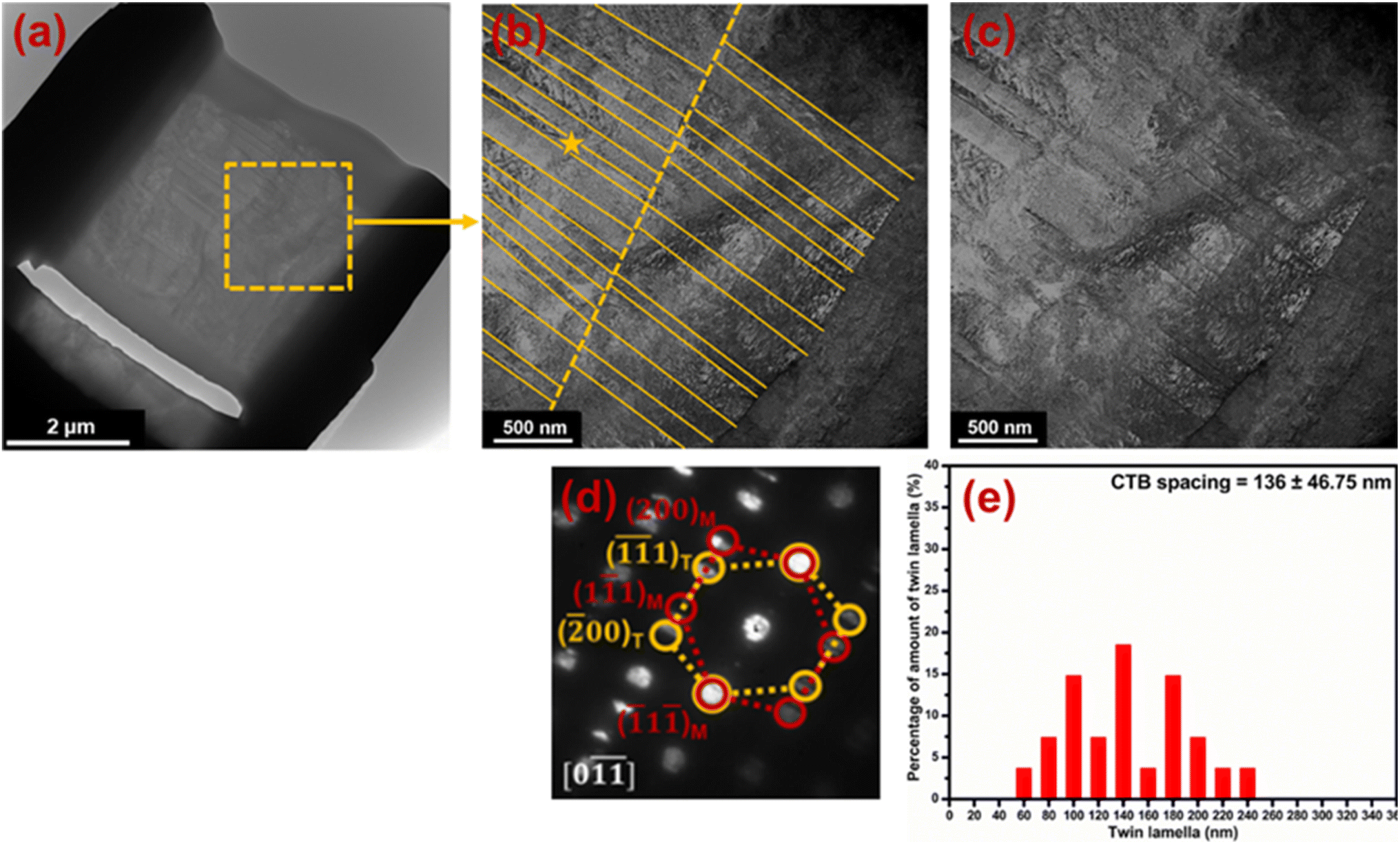 | ||
| Fig. 6 TEM bright-field images of Cu plated at 0.5 L·min−1 for (a) the entire copper sheet, and the HRTEM images within the yellow-bordered region shown in (b) with annotation lines (solid lines refer to twin boundaries and dashed lines refer to grain boundaries) and in (c) without annotations. (d) The SAED image taken at the star-marked location in (b). (e) The twin distribution identified within the same region. | ||
 | ||
| Fig. 7 TEM bright-field images of Cu plated at 2.5 L·min−1 for (a) the entire copper sheet with the HRTEM images within the yellow-bordered region shown in (b) with annotation lines (solid lines refer to twin boundaries and dashed lines refer to grain boundaries) and in (c) without annotations. (d) The SAED image taken at the star-marked location in (b). (e) The twin distribution identified within the same region. | ||
The twin lamella spacing was found to be tunable by adjusting the aeration flow rate at the cathode in Fig. 6 and 7. For the copper foil prepared at the aeration flow rate of 0.5 L·min−1, the twin lamellae are thicker and less uniformly distributed, with an average spacing of 136 nm and a standard deviation of 46.75 nm (see Fig. 6). Conversely, the copper foil prepared at the aeration flow rate of 2.5 L·min−1, the lamellae are thinner and more evenly distributed, with an average spacing of 61.37 nm and a standard deviation of 37.67 nm from Fig. 7. The selected area electron diffraction (SAED) images exhibit the typical, symmetrical diffraction patterns attributable to the nanotwinned structure, in a good agreement with previous studies.15,47–51 These findings are consistent with the FIB and EBSD data presented in Fig. 5(d), 4(c and d).
The nanotwinned distributions of copper foil electroplated at the aeration flow rates of 0.5 L·min−1 and 2.5 L·min−1 are presented in Fig. 8(a). Moreover, we conduct the sheet resistance testing, shown in Fig. 8(b). With the altered twin spacing, the copper foil exhibits distinguishable sheet resistance. According to the literature,52 the interfacial energy of twin boundary is normally an order of magnitude smaller than the conventional high-angle grain boundary, meanwhile the electrons in crystals are transported along grain or twin boundaries. Thus, introducing the nanotwinned structure inside the copper foil may change their conductivity. In Fig. 8(b), the conductivity of the copper foil with a higher density of nanotwins is higher, indicating that the nanotwinned structure in the (111)-oriented copper lattice can enhance the electrical properties. The higher twin boundaries within the copper foil, the higher the conductivity of the resultant Cu foil. Besides, the variation of the sheet resistance on the copper foil plated at 2.5 L·min−1 is small, in accordance with the twin distribution displayed in Fig. 8(a).
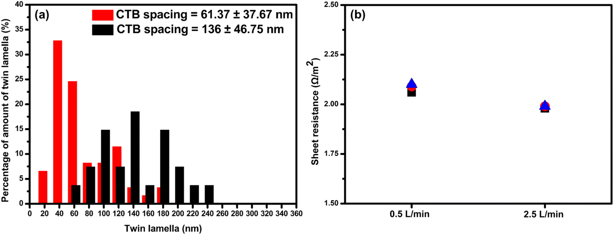 | ||
| Fig. 8 (a) The distributions of twin spacing collected from the bright field HRTEM images and (b) the sheet resistance of the Cu foil electroplated at the aeration flow rates of (black bars) 0.5 L·min−1 and (red bars) 2.5 L·min−1. | ||
3.6. The mechanism for inducing the twin distribution
Copper, a metal characterized by its low stacking fault energy (SFE),53,54 tends to form partial and extended dislocations which act to reduce the strain energy associated with the dislocation slip, despite the slight increase in the copper lattice energy. These partial dislocations facilitate the formation of twins in the copper lattice, where the distance between adjacent extended dislocations defines the twin spacing.As found in Fig. 2, by adjusting the aeration flow rate at the cathode surface from 0.5 L·min−1 to 2.5 L·min−1, a reduced chloride ion coverage is achieved, forming more ordered, sparse layers of adsorbed chloride ions. These reduced ad-layers exhibit lower competition for adsorption sites with MPS compared to the case employing a lower aeration flow rate. Also, a higher aeration flow directly enhances the MPS adsorption due to the lower MPS consumption in the parasitic side reactions (MPS cycle), as displayed in Fig. 9(c) and a reduced diffusion layer at the electrode. Consequently, as shown in Fig. 9, because of a higher aeration flow rate, the enhanced MPS activity decreases the overall overpotential, facilitating the copper deposition. This favors the growth of uniform and large protrusions, and the high crystallinity of copper grains, which are energetically correlated with the reduced copper lattice energy induced by the enhanced MPS activity.
 | ||
| Fig. 9 The schemes of (a) merely Cl− and (b) Cl−/MPS adsorption near the cathode by electroplating at the aeration flow rates of (1) 0.5 L·min−1 and (2) 2.5 L·min−1. (c) The details of the MPS cycle. | ||
In the high-current-density dc electroplating, the heat generated at the cathode substrate probably transfers into the copper lattice rapidly. This thermal gradient allows Cu atoms to diffuse and induces dislocations, which migrate along the growth direction of the copper nucleation and growth. The combination of a high aeration flow rate and the convection-sensitive chloride ions and MPS further reduces the copper lattice energy in the 2.5 L·min−1 case, allowing it to endure the excess energy introduced by the formation of the nanotwinned structure. Thus, in a high-speed copper electroplating system employing CuSO4 with additives of chloride ions and MPS, the increased aeration flow at low temperatures induces the formation of a densely packed (111)-oriented nanotwinned structure within the copper matrix. Furthermore, the increased density of the nanotwinned structure should facilitate stress relaxation, thereby reducing the residual stress and mitigating the formation of vertical stacking faults. These faults, if left unchecked, can slip and disrupt the integrity of the nanotwinned structure, particularly under thermal stress. Consequently, the higher aeration flow fosters the development of a denser and mechanically more stable nanotwinned copper structure, as illustrated in Fig. 10.
 | ||
| Fig. 10 The schemes of forming (a) the partial and extended dislocations and (b) the nanotwinned structure by electroplating at the aeration flow rates of (1) 0.5 L·min−1 and (2) 2.5 L·min−1. | ||
4. Conclusions
Adjusting the aeration flow rate near the cathode in a CuSO4-based electroplating system could successfully modify the twin lamella distribution from an average twin spacing of 61.37 nm to 136 nm at an aeration flow rate of 2.5 L·min−1 and 0.5 L·min−1, respectively. This phenomenon results from the changes in the adsorption situation and coverage of chloride ions and MPS on the cathode surface, causing the variable effect of additives in the electroplating system. The mere control of aeration flow rates could manufacture the high texture (111)-oriented nanotwinned copper composed of altered nanotwin distributions at the high deposition rate of 400 mA·cm−2 in the dc mode without violently changing the crystal orientation, grain size, and morphology, which could be a good candidate material to determine the influence of twin distributions in various industry applications.Data availability
Data will be made available from the authors on reasonable request.Conflicts of interest
There are no conflicts to declare.Acknowledgements
The financial support of this work, by National Science and Technology Council (NSTC) of Taiwan under contract no. NSTC 112-2923-E-007-005 and the Ministry of Science and Technology (MOST) of Taiwan under contract no. MOST 111-2221-E-007-006-MY3, is gratefully acknowledged.References
- L. Yuhang, Y. Li, J. Sun, Z. Du, X. Hu, J. Bi, C. Liu, W. Ai and Q. Yan, Nano Res. Energy., 2023, e9120048 Search PubMed.
- J. Zhou, J. Qin and H. Zhan, ChemPhysChem, 2024, 25, e202400007 CrossRef CAS PubMed.
- L. Lu, Y. Shen, X. Chen, L. Qian and K. Lu, Science, 2004, 304, 422–426 CrossRef CAS PubMed.
- Z. You, X. Li, L. Gui, Q. Lu, T. Zhu, H. Gao and L. Lu, Acta Mater., 2013, 61, 217–227 CrossRef CAS.
- M. Dao, L. Lu, Y. Shen and S. Suresh, Acta Mater., 2006, 54, 5421–5432 CrossRef CAS.
- K.-C. Chen, W.-W. Wu, C.-N. Liao, L.-J. Chen and K.-N. Tu, Science, 2008, 321, 1066–1069 CrossRef CAS.
- O. Anderoglu, A. Misra, H. Wang and X. Zhang, J. Appl. Phys., 2008, 103, 094322 CrossRef.
- W. Zhao, N. Tao, J. Guo, Q. Lu and K. Lu, Scripta Mater., 2005, 53, 745–749 CrossRef CAS.
- B. Roy and J. Das, Sci. Rep., 2017, 7, 17512 CrossRef.
- O. Anderoglu, A. Misra, H. Wang, F. Ronning, M. Hundley and X. Zhang, Appl. Phys. Lett., 2008, 93, 083108 CrossRef.
- D. Xu, W. L. Kwan, K. Chen, X. Zhang, V. Ozoliņš and K.-N. Tu, Appl. Phys. Lett., 2007, 91, 254105 CrossRef.
- D. Xu, V. Sriram, V. Ozolins, J.-M. Yang, K.-N. Tu, G. R. Stafford and C. Beauchamp, J. Appl. Phys., 2009, 105, 023521 CrossRef.
- R. Winand, Electrochim. Acta, 1994, 39, 1091–1105 CrossRef.
- M. Hasegawa, M. Mieszala, Y. Zhang, R. Erni, J. Michler and L. Philippe, Electrochim. Acta, 2015, 178, 458–467 CrossRef.
- X. Zhan, J. Lian, H. Li, X. Wang, J. Zhou, K. Trieu and X. Zhang, Electrochim. Acta, 2021, 365, 137391 CrossRef.
- C.-L. Huang, W.-L. Weng, C.-N. Liao and K.-N. Tu, Nat. Commun., 2018, 9, 340 CrossRef PubMed.
- S.-T. Liu, H.-Y. Ku, C.-L. Huang and C.-C. Hu, Electrochim. Acta, 2022, 430, 141011 CrossRef.
- C.-L. Huang and C.-N. Liao, Appl. Phys. Lett., 2015, 107, 021601 CrossRef.
- C.-C. Lin and C.-C. Hu, J. Electrochem. Soc., 2020, 167, 082505 Search PubMed.
- T. M. Huynh, F. Weiss, N. T. Hai, W. Reckien, T. Bredow, A. Fluegel, M. Arnold, D. Mayer, H. Keller and P. Broekmann, Electrochim. Acta, 2013, 89, 537–548 Search PubMed.
- T. Okubo, K. Watanabe and K. Kondo, J. Electrochem. Soc., 2007, 154, C181 CrossRef.
- M. A. Thorseth, M. Scalisi, I. Lee, S.-M. Park, Y.-H. Lee, J. Prange, M. Imanari, M. Lefebvre and J. Calvert, Additional Papers and Presentations, 2016, vol. 2016, pp. 000631–000649 Search PubMed.
- C.-C. Lin, C.-H. Yen, S.-C. Lin, C.-C. Hu and W.-P. Dow, J. Electrochem. Soc., 2017, 164, D810 CrossRef.
- N. T. Hai, K. W. Krämer, A. Fluegel, M. Arnold, D. Mayer and P. Broekmann, Electrochim. Acta, 2012, 83, 367–375 CrossRef.
- S. Choe, M. J. Kim, H. C. Kim, S. K. Cho, S. H. Ahn, S.-K. Kim and J. J. Kim, J. Electrochem. Soc., 2013, 160, D3179 CrossRef.
- I. Burrows, J. Harrison and J. Thompson, J. Electroanal. Chem. Interfacial Electrochem., 1975, 58, 241–249 CrossRef CAS.
- J. Harrison, D. Sandbach and P. Stronach, Electrochim. Acta, 1979, 24, 179–189 CrossRef CAS.
- I. Burrows, K. Dick and J. Harrison, Electrochim. Acta, 1976, 21, 81–84 CrossRef CAS.
- K. G. Schmitt, R. Schmidt, H. F. Von-Horsten, G. Vazhenin and A. A. Gewirth, J. Phys. Chem. C, 2015, 119, 23453–23462 CrossRef CAS.
- W. M. Latimer, The Oxidation States of the Elements and Their Potentials in Aqueous Solutions, 1938 Search PubMed.
- A. Bard, Standard Potentials in Aqueous Solution, Routledge, 2017 Search PubMed.
- T. Hayashi and M. Yokoi, Denki Kagaku oyobi Kogyo Butsuri Kagaku, 1979, 47, 654–660 CrossRef CAS.
- C. Ehlers, I. Villegas and J. Stickney, J. Electroanal. Chem. Interfacial Electrochem., 1990, 284, 403–412 CrossRef CAS.
- M. Vogt, A. Lachenwitzer, O. Magnussen and R. Behm, Surf. Sci., 1998, 399, 49–69 CrossRef CAS.
- T. P. Moffat and L.-Y. O. Yang, J. Electrochem. Soc., 2010, 157, D228 CrossRef CAS.
- W. Li, Y. Wang, J. Ye and S. Li, J. Phys. Chem. B, 2001, 105, 1829–1833 CrossRef CAS.
- W.-P. Dow and H.-S. Huang, J. Electrochem. Soc., 2005, 152, C67 CrossRef CAS.
- T.-Y. Yu, H. Lee, H.-L. Hsu, W.-P. Dow, H.-K. Cheng, K.-C. Liu and C.-M. Chen, J. Electrochem. Soc., 2016, 163, D734 CrossRef CAS.
- M. Raja, J. Subha, F. B. Ali and S. H. Ryu, Mater. Manuf. Processes, 2008, 23, 782–785 CrossRef CAS.
- T.-C. Chan, Y.-L. Chueh and C.-N. Liao, Cryst. Growth Des., 2011, 11, 4970–4974 CrossRef CAS.
- B. Hong, C.-h. Jiang and X.-j. Wang, Surf. Coat. Technol., 2007, 201, 7449–7452 CrossRef CAS.
- K. Kondo, R. N. Akolkar, D. P. Barkey and M. Yokoi, Copper Electrodeposition for Nanofabrication of Electronics Devices, Springer, 2014 Search PubMed.
- G. Cheng, H. Li, G. Xu, W. Gai and L. Luo, Sci. Rep., 2017, 7, 12393 CrossRef.
- Y. Y. Lim and M. M. Chaudhri, Philos. Mag. A, 2002, 82, 2071–2080 Search PubMed.
- J. Chu and T. Lin, J. Appl. Phys., 1999, 85, 6462–6469 CrossRef.
- Z.-G. Li, L.-Y. Gao, Z. Li, R. Sun and Z.-Q. Liu, J. Mater. Sci., 2022, 57, 17797–17811 CrossRef.
- N. Lu, K. Du, L. Lu and H. Ye, Nat. Commun., 2015, 6, 7648 CrossRef PubMed.
- T. E. J. Edwards, N. Rohbeck, E. Huszár, K. Thomas, B. Putz, M. N. Polyakov, X. Maeder, L. Pethö and J. Michler, Adv. Sci., 2022, 9, 2203544 CrossRef.
- L. Sun, X. He and J. Lu, npj Comput. Mater., 2018, 4, 6 CrossRef.
- L. Lu, X. Chen, X. Huang and K. Lu, Science, 2009, 323, 607–610 CrossRef PubMed.
- C. L. Huang, K. Sasaki, D. Senthil Raja, C. T. Hsieh, Y. J. Wu, J. T. Su, C. C. Cheng, P. Y. Cheng, S. H. Lin and Y. Choi, Adv. Energy Mater., 2021, 11, 2101827 CrossRef.
- K. Lu, Nat. Rev. Mater., 2016, 1, 1–13 Search PubMed.
- Y. Zhao, X. Liao, Y. Zhu, Z. Horita and T. Langdon, Mater. Sci. Eng., A, 2005, 410, 188–193 CrossRef.
- A. Rohatgi, K. S. Vecchio and G. T. Gray, Metall. Mater. Trans. A, 2001, 32, 135–145 CrossRef.
Footnote |
| † These authors contributed equally to this work. |
| This journal is © The Royal Society of Chemistry 2025 |