
 Open Access Article
 This Open Access Article is licensed under a Creative Commons Attribution-Non Commercial 3.0 Unported Licence
Economical 550 V energy harvesting from plastic and electronic waste using human motions†
Man
Singh‡
a,
Sameer
Kumar‡
a,
Alankar
Kafle
a,
Kalpana
Garg
a,
Parimal
Sharma
b,
C. C.
Reddy
b and
Tharamani C.
Nagaiah
 *a
*a
aDepartment of Chemistry, Indian Institute of Technology Ropar, Rupnagar-140001, Punjab, India. E-mail: tharamani@iitrpr.ac.in
bDepartment of Electrical Engineering, Indian Institute of Technology Ropar, Rupnagar-140001, Punjab, India
First published on 17th January 2025
Abstract
Waste management of plastic and electronic artefacts is a very tedious task and requires a great deal of expense. The pressing threat to the environment due to excessive plastic use and uncategorized electronic waste management demands versatile strategies to mitigate the mentioned issues. Herein, we have showcased a very economical and straightforward approach to utilize plastic and electronic waste for designing a triboelectric nanogenerator (TENG). Polyethylene terephthalate (PET) recovered from used Kapton tape and, printing paper were utilized as triboelectric layers. More importantly, for the fabrication of the electrode layers, sophisticated and expansive techniques were replaced by a simple sacrificial electrodeposition of copper. Discarded electric wires from damaged UPS batteries were used as the source of copper. The fabricated TENG delivered excellent electric output with a maximum open circuit voltage of ∼552 V, a short circuit current of 18.8 μA and a high-power density of 7.68 W m−2 under contact-separation triggered by human hand tapping. Additionally, the device exhibited a high open-circuit voltage of 615 V under vertical contact-separation driven by a custom-built linear motor, which is approximately 2 and 4 times greater than that of the TENG devices fabricated with Cu-tape and carbon electrodes, respectively. A vast number of practical demonstrations include the successful lighting of 472 LEDs connected in series, storing the charges in commercial capacitors, and powering a digital calculator. Furthermore, we demonstrated the potential application of e-Cu@WPP-TENG to power LED panels for advertisement boards, logos, nameplates, and similar displays in hotels, restaurants, buildings, laboratories, and homes. We believe that this work stresses the importance of implementing economically viable strategies for utilizing plastic and electronic waste to harvest valuable energy.
Introduction
Accelerated technical advancement and modernization propels the production and consumption of electronic equipment along with plastic merchandise. Every year approximately 359 million tons of plastic is produced over the globe and 150–200 million tons of plastic waste end up in landfills or sea-water.1 Excessive plastic use has posed a major threat to the environment. To mitigate the impact of plastics on the environment, global movements promote cutting down plastic usage, encouraging their reuse, and recycling for the foreseeable future. As per the 2018 report by McKinsey, 50% of plastics worldwide could be reused or recycled by 2030 and can generate a profit-pool growth of approximately $60 billion.2 Recently, various scientific reports have highlighted the utilization of plastic waste by converting it into value-added products.3–9 For instance, various applications target carbon dioxide (CO2) capture and utilization via chemical treatment of waste plastics.10–14 Moreover, there has been a significant development in the exploration of waste plastic materials for energy storage applications in batteries and supercapacitors.15–18 Meanwhile, apart from plastic waste, generation of E-waste (electronic waste) from dead batteries and discarded components of electronic devices is also increasing which can be detrimental if neglected.19 According to the recent reports the expected E-waste all over the world could reach 112 million tons by the year 2050.20,21 Unfortunately, E-waste in the form of old cable wires is often ignored and thrown in piles as they do not have direct harmful effects. However, these can be of high economic value due to precious Cu and Al metals.22,23 Thus, it would be worth transforming the waste into wealth by recycling or reusing these wires. In the context of the foregoing discussion, it is imperative to develop sustainable technologies for E-waste and plastic waste recycling from the perspective of both economic value and environmental protection. Over the past decade, triboelectric nanogenerators (TENGs) have emerged as a sustainable energy harvesting technology which is based on the conjunction of the triboelectric effect and electrostatic induction.24 Typically, a TENG device consists of two dissimilar triboelectric materials i.e. electron-donating (tribo-positive) and electron-accepting (tribo-negative) materials attached to the electrode layers (Scheme 1a).25 The basis of material selection is their electron affinity as proposed in the triboelectric series.26 In principle, greater difference in electron affinity of triboelectric materials will lead to better electrical outputs of TENGs. Among them, plastic materials with heteroatom functionalities such as polyethylene terephthalate (PET), polytetrafluorethylene (PTFE), polyvinylidene fluoride (PVDF), etc. can be used as tribo-negative materials by facilitating in the accumulation of negative surface charges when brought into contact with tribo-positive materials.27–32 Lately, a soft aerogel from scrap PET bottles was reported to fabricate a TENG which delivered a peak voltage of 67.7 V and a short-circuit current of 9.4 μA with a high power density of 5.57 W m−2.33 Moreover, Kapton tape (used in PCB circuit boards, insulating electrical wires and coils, etc.) comes with a plastic adhesive and this plastic is usually thrown away after peeling the Kapton layer (Scheme 1b). However, this plastic exhibits a PET structure and therefore, instead of discarding, it can be utilized as a tribonegative material for the TENG. Nevertheless, the selection of tribo-positive materials is just as crucial. In that regard, cellulose-based materials are suitable tribo-positive materials considering their easy availability, low cost, biodegradability and the presence of electron donating functionalities.34–38 Recently, tissue paper was reported as a tribo-positive material against a polyimide film (tribo-negative material) to achieve an open-circuit voltage of ∼450 V, short-circuit current of 5.5 μA and peak power of ∼1.4 mW under mechanical stimulation.39 | ||
| Scheme 1 Schematic representation of (a) basic components of a TENG, (b) waste plastic from Kapton tape and E-waste from electric cables of old UPS, (c) utilization of plastic and E-waste for fabrication of electrode layers using electrodeposition, (d) fabrication of e-Cu@WPP-TENG, (e) working of e-Cu@WPP-TENG under hand tapping movement and demonstration of its applications in lighting LEDs, capacitor charging and powering calculators. | ||
More importantly, regardless of choosing an appropriate triboelectric layer, the fabrication of the electrode layer on top of the triboelectric layer is critical because electrostatic induction generates opposite charges at the interface of both layers. A minimum barrier between these layers ensures better development of charges. Generally, two common approaches are involved in the preparation of electrode layers, one via simple pasting or glueing of metal tapes such as aluminium, copper, etc. on triboelectric layers.40–42 Despite being a relatively simple process, it leads to greater interfacial resistance between triboelectric and electrode layers. While the other approach involves sophisticated techniques viz., photolithographic patterning, electrospinning and thermal evaporation of expensive metals such as gold, silver, etc. to deposit thin films on triboelectric layers. Although this method provides high electrical outputs, they demand high fabrication costs.32,43–47 Thus, development of a cost-effective approach ensuring smaller contact resistance with the triboelectric layer is the need of the hour.
Therefore, in the present work we have utilized discarded plastic waste from Kapton tape as a tribo-negative material, and low cost and biodegradable ordinary printing paper as the tribo-positive material. The electrode layers were fabricated via a simple, quick and greener approach viz. sacrificial electrodeposition of copper from damaged electrical wires (Scheme 1c). The fabricated triboelectric nanogenerator (e-Cu@WPP-TENG) as shown in Scheme 1d delivered an outstanding electrical performance with an open-circuit voltage of 552 V, a short-circuit current of 18.8 μA and a high-power density of 7.68 W m−2 under a mechanical stimulus provided by human hand pressing. The working principle of the device involves the generation of alternating current during pressing and releasing movements of a human hand in the vertical contact-separation mode (Scheme 1e). Furthermore, the practical application of the fabricated TENG was demonstrated by charging the capacitors of different capacitance values viz., 1 μF, 2.2 μF and 4.7 μF to 10 V in less than a minute. Furthermore, the application was extended to power a digital calculator and LED panels for advertisement or address boards (Scheme 1e). Consequently, the as-fabricated e-Cu@WPP-TENG from plastic and E-waste combined with a simple electrodeposition approach for the preparation of electrode layers is a novel and sustainable strategy for waste-to-energy transformation.
Results and discussion
A triboelectric nanogenerator was fabricated using waste plastic taken from used Kapton (polyimide) tape (Fig. S1†) and bio-based materials viz. cellulose paper as tribo-negative and tribo-positive layers, respectively. Initially, we have performed X-ray diffraction (XRD) and Fourier transform infrared (FT-IR) spectroscopic analysis to identify the basic characteristics of the waste plastic sheet. The peaks at ∼23° and 26° in the XRD pattern (Fig. 1a) match with the characteristic crystalline (110) and (100) planes of polyethylene terephthalate (PET), respectively.48 Furthermore, the FT-IR spectra (Fig. 1b) reveal peaks at 1711 cm−1, 1340 cm−1 and 1235 cm−1 corresponding to stretching frequencies of C![[double bond, length as m-dash]](https://www.rsc.org/images/entities/char_e001.gif) O, C–O and CC from carbonyl, ester, and a phenyl ring of the PET polymeric structure (Fig. 1c), respectively.49 The presence of these electronegative groups indicates the existence of tribo-negative properties in the plastic sheet. To pair the tribonegativity of the plastic sheet with a suitable tribo-positive material we have chosen ordinary printing paper due to the presence of electron donor groups in the cellulose chains.50 The XRD and FT-IR spectra of the paper sheet exhibited the characteristic cellulose framework (Fig. S2†).
O, C–O and CC from carbonyl, ester, and a phenyl ring of the PET polymeric structure (Fig. 1c), respectively.49 The presence of these electronegative groups indicates the existence of tribo-negative properties in the plastic sheet. To pair the tribonegativity of the plastic sheet with a suitable tribo-positive material we have chosen ordinary printing paper due to the presence of electron donor groups in the cellulose chains.50 The XRD and FT-IR spectra of the paper sheet exhibited the characteristic cellulose framework (Fig. S2†).
 | ||
| Fig. 1 (a) X-ray diffraction pattern, (b) FT-IR spectra of the waste plastic sheet, (c) chemical structure of PET, and (d) experimental setup for electrodeposition of Cu over carbon coated plastic and paper sheets. Digital photographs of electrodeposited Cu over (e) plastic & (f) paper substrates. | ||
Furthermore, to prepare the electrode layers of the TENG, primarily the non-conductive plastic and paper sheets were coated with Vulcan carbon (Vulcan XC-72R carbon) on one side of the sheet (Fig. S3 & S4†) followed by copper deposition via electrodeposition. The Cu was electrodeposited using a bundle of copper wires recovered from electronic waste (Fig. 1d, detailed in ESI Fig. S5–S7†).
The electrodeposited plastic and paper are denoted as e-Cu@plastic and e-Cu@paper respectively, which served as electrode layers for the fabrication of TENG (Fig. 1e and f). The XRD patterns of e-Cu@plastic and e-Cu@paper exhibit the characteristic (111), (200) and (220) planes corresponding to metallic Cu (COD-CIF#: 4105681, Fig. 2a) signifying the successful deposition of copper. Energy dispersive X-ray spectroscopy (EDS) and elemental dot mapping further validated the presence of Cu (Fig. S8 & S9†). The morphological features characterized by FESEM (Fig. 2b and c) revealed the hexagonal copper particles decorated over the plastic sheet, while on the paper comparatively bigger star-shaped copper particles (Fig. 2d and e) were observed.
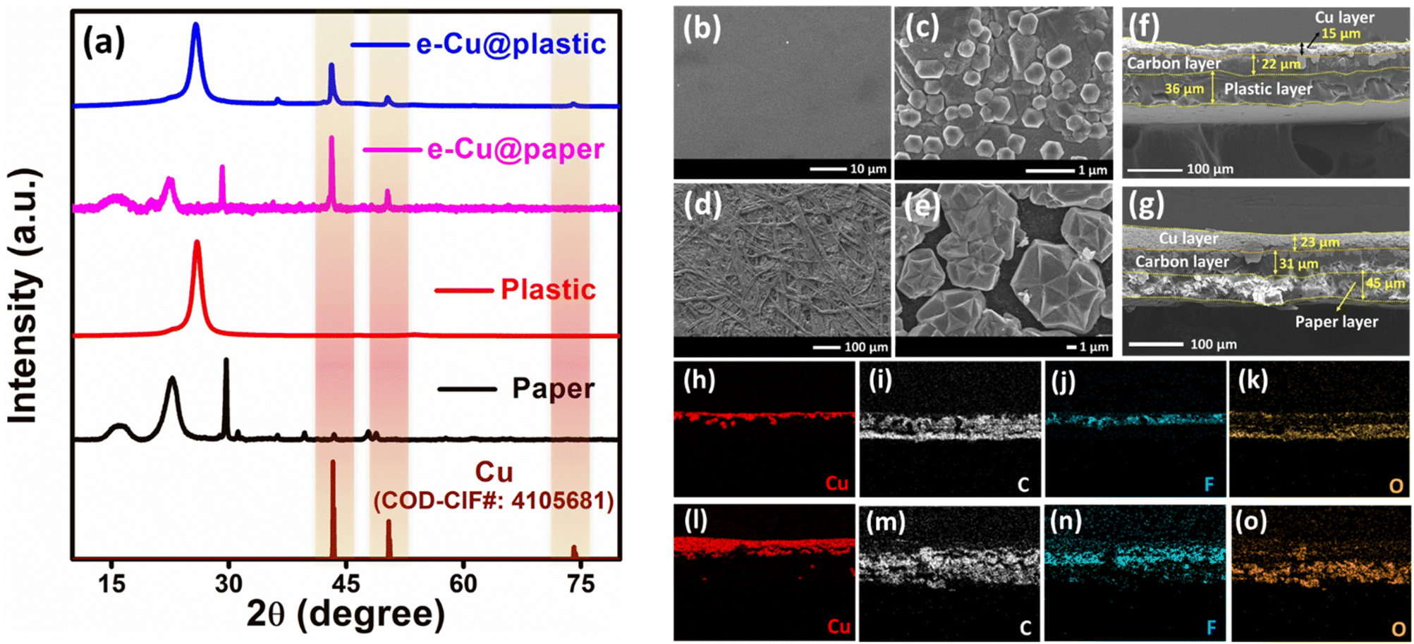 | ||
| Fig. 2 (a) X-Ray diffraction patterns of various samples for a TENG. FESEM images of (b) plastic, (c) e-Cu@plastic, (d) paper, and (e) e-Cu@paper. Cross-sectional FESEM images of (f) e-Cu@plastic & (g) e-Cu@paper. Elemental dot mapping images of (h)–(k) e-Cu@plastic and (l)–(o) e-Cu@paper. | ||
The cross-sectional FESEM images were captured to analyze the different layers of samples after the electrodeposition of Cu. The cross sectional view of the electrode in FESEM images (Fig. 2f) clearly demonstrates various layers of the electrode, viz., Cu at the top layer, followed by carbon at the middle, and plastic layers at the bottom in the tribonegative material (plastic) with a layer thickness of ∼15 μm, 22 μm and 36 μm respectively (Fig. 2f). The corresponding EDS dot mapping showed the presence of Cu, C, F & O elements in the respective layers (Fig. 2h–k and S10a†). Similarly, the electrodeposited Cu over paper (tribopositive) exhibits Cu (top), carbon (middle) and a paper (bottom) layer with a layer thickness of ∼23 μm, 31 μm and 45 μm respectively (Fig. 2g, l–o & S10b†). The prepared tribonegative and tribopositive electrodes were utilized to fabricate a TENG denoted as e-Cu@WPP-TENG. The uncoated sides of plastic and paper sheets with dimensions of 4 cm × 3 cm were made to face each other in a vertical contact-separation mode. Cu-coated sides were utilized as bottom and top electrodes connected through Cu wires in the external circuit (Fig. 3a). For comparison, two control devices were also fabricated by (i) using carbon-coated waste plastic and paper as electrode layers (C@WPP-TENG) and (ii) attaching the copper tapes as electrode layers (Cu-tape@WPP-TENG) as shown in Fig. S11 and S12† respectively.
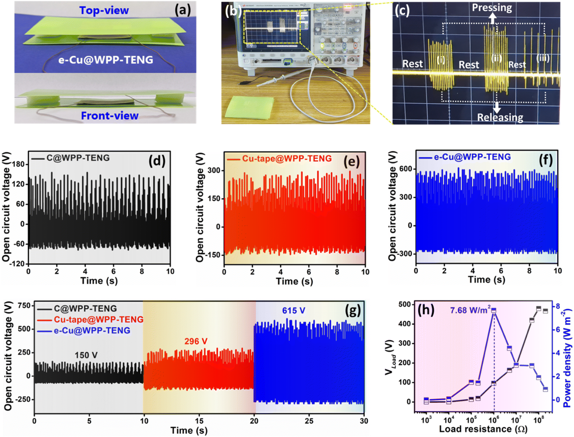 | ||
| Fig. 3 (a) Digital photograph of the assembled e-Cu@WPP-TENG, (b) instrumental setup for recording the electrical signal of e-Cu@WPP-TENG, and (c) signal response of e-Cu@WPP-TENG under different modes of hand pressing. Open circuit voltages of (d) C@WPP-TENG, (e) Cu-tape@WPP-TENG & (f) e-Cu@WPP-TENG, (g) comparison of open-circuit voltages of different devices, and (h) plot of voltage and power density with varying load resistance for e-Cu@WPP-TENG. | ||
The electrical response of e-Cu@WPP-TENG was recorded using a digital oscilloscope under mechanical stimulation introduced by hand tapping (Fig. 3b). The electrical response varied under different types of hand-pressing movements. Fig. 3c shows the electrical output under (i) rapid-soft, (ii) rapid-hard and (iii) slow-hard hand pressing of e-Cu@WPP-TENG (Movie S1†). It was evident that the hard pressing movements provide higher signal magnitude while the rapid pressing helps in maintaining the signal response with narrow gaps. This observation is in agreement with the fact that the signal magnitude is dependent on the mechanical force applied and independent of the frequency.51 The open-circuit voltages (Voc) of fabricated TENG devices were measured by hand pressing under similar conditions (Fig. S13†). e-Cu@WPP-TENG displayed a high open-circuit voltage of 552 V which is 11 and 3 times higher than those in the case of C@WPP-TENG (49 V) and Cu-tape@WPP-TENG (181 V) respectively (Fig. S14†). Moreover, the individual responses of TENG devices in a 1 s timeframe showed five recorded signals on an average with a stable peak-to-peak Voc (sum of forward and reverse signals) of 73 V, 237 V and 792 V respectively for C@WPP-TENG, Cu-tape@WPP-TENG and e-Cu@WPP-TENG (Fig. S15†). Short circuit current (Isc) is another key parameter for TENG devices; hence, the measurement of Isc was carried out by using a full wave rectifier in the circuit. The obtained current responses shown in Fig. S16† indicated four times higher Isc for e-Cu@WPP-TENG (18.8 μA) as compared to that of Cu-tape@WPP-TENG (4.7 μA) which again highlights the superior electrical performance of e-Cu@WPP-TENG. Moreover, to rigorously compare the electric outputs of TENG devices, a simple homemade machine was designed to provide consistent vertical contact-separation (Fig. S17†). Fig. 3d–f indicate that the Voc obtained under the mechanical motion provided by a custom built machine is considerably higher and more stable compared to those of hand pressing movements. The comparison of electrical outputs (Fig. 3g) of the three devices was performed under same mechanical input conditions which indicated that e-Cu@WPP-TENG showed a high Voc of 615 V which is approximately 2 and 4 times higher than that of Cu-tape@WPP-TENG (296 V) and C@WPP-TENG (150 V), respectively. The higher outputs of devices with Cu electrode layers indicate that the metal electrodes are better for charge induction compared to carbon electrodes. This can be correlated with the higher electrical resistance offered by the carbon coating compared to that of the metallic copper layer which was supported by the experimental evidence recorded via a digital multimeter (Fig. S18–S21†). Moreover, the superior performance of e-Cu@WPP-TENG compared to Cu-tape@WPP-TENG can be attributed to the better interfacial contact and effective charge induction on the electrodeposited Cu layer.
To further investigate the performance of e-Cu@WPP-TENG, various loads of resistances ranging from 1 kΩ to 200 MΩ were applied to record the electrical outputs. The output voltage (VLoad) was found to increase with increasing resistance as expected from Ohm's law (V = IR) (Fig. 3h). Moreover, the power density at different load resistances was calculated using the following relation:52
| P = VLoad2/RLoad × A | (1) |
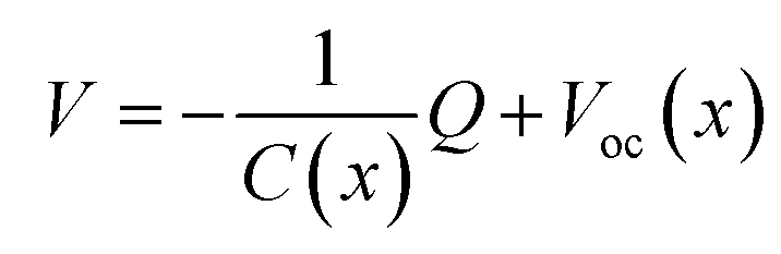
To understand the mechanism of charge generation and electrification, a working model of e-Cu@WPP-TENG is postulated schematically in Fig. 4. The underlying working principle is based on the conjunction of the triboelectric effect or contact electrification and electrostatic induction.53 The contact electrification leads to static polarized charges and electrostatic induction is responsible for the conversion of mechanical energy to electricity.54 The mechanism of e-Cu@WPP-TENG is explained under open-circuit (Fig. 4a) and short-circuit conditions (Fig. 4b). Under open-circuit conditions, the electrodes are connected to a digital oscilloscope with infinitely large impedance, effectively preventing current flow between the electrodes. Similarly, under short-circuit conditions, the electrodes are shorted before being connected to a highly sensitive electrometer. When contact is made between the triboelectric layers via hand pressing, the generation of surface charges at contact areas takes place due to the triboelectric effect53,55 [Fig. 4a(i) & b(i)]. The nature of charges depends upon the electron affinity of triboelectric layers and their relative positions in the triboelectric series.56,57 Plastic (PET) due to its higher electron affinity develops negative charges on its surface, whereas paper (cellulose) due to its electron-donating nature develops positive surface charges.50 Now due to the dielectric nature of these triboelectric layers, the charges have a long retention time and are confined to surfaces.58–60 Therefore, practically no electric potential difference is generated between the electrodes attached to the respective triboelectric layers. Once the pressing force is removed the electrostatic induction of the opposite charge takes place on the electrode layers which creates a electric potential difference between the electrodes. As a result, the generation of voltage (Voc) takes place under open-circuit conditions (Fig. 4a(ii)) and the current starts to flow from the bottom electrode to the top electrode in the external circuit under short-circuit conditions [Fig. 4b(ii)]. According to the theoretical model given by Niu and Wang, the electric potential difference (V) between electrodes can be expressed by using the equation:54,61
 | (2) |
 | ||
| Fig. 4 Schematic representation of the working mechanism of e-Cu@WPP-TENG at different stages of contact and separation under (a) open circuit conditions and (b) short-circuit conditions, (c) COMSOL simulation snapshots for e-Cu@WPP-TENG at various separation distances, and (d & e) zoomed-in portion of TENG devices for COMSOL simulation at a separation distance of 0.001 m. | ||
Furthermore, Fig. S23† shows the schematic comparison of electrode layers attached to triboelectric layers in Cu-tape@WPP-TENG and e-Cu@WPP-TENG. In the case of Cu-tape as an electrode layer, there is additional resistance between triboelectric and electrode layers due to the adhesive in the tape which weakens the interfacial contact and leads to poor charge induction at the electrode surface (Fig. S23a†). Whereas, in the case of e-Cu@WPP-TENG, the copper layer is electrodeposited over carbon-precoated substrates without any adhesive tape (Fig. S23b†). Therefore, there is no blockage between the triboelectric and electrode layers leading to better and effective charge induction at the electrode surface. This might be a probable explanation for the superior electrical outputs of e-Cu@WPP-TENG compared to the Cu-tape@WPP-TENG device. To support this hypothesis, the COMSOL simulation studies were carried out for the e-Cu@WPP-TENG and Cu-tape@WPP-TENG devices. Fig. 4e & S24† show the simulation results of Cu-tape@WPP-TENG and e-Cu@WPP-TENG devices at various separation distances (∼0 to 0.02 m) between the dielectric layers. As the separation between the triboelectric layers increased, the surface potential also increased, aligning with the experimental results. Furthermore, a comparison of Cu-tape@WPP-TENG was obtained at the initial and final separation distances (Fig. 4d, e & S25†). The non-conductive adhesive layers in the Cu-tape@WPP-TENG device serve as additional dielectrics, significantly reducing the electrostatic charge induction at the electrode layers compared to e-Cu@WPP-TENG.
Since the electrical outputs of the TENG are subjected to the availability of an external mechanical source and are prone to fluctuations, the storage of harvested energy becomes very important. Therefore, the energy harvested by e-Cu@WPP-TENG was stored in commercial capacitors for effective applications in practical scenarios. The energy stored in the capacitor can further be used to run stable applications of any external load connected to the circuit. As the majority of the electronic devices require a direct current (DC) supply, a full wave rectifier was implanted in the electric circuit to convert the AC signal from e-Cu@WPP-TENG to a DC supply for charging the capacitor (Fig. 5a). First, the charging of a 1 μF capacitor under hand pressing of e-Cu@WPP-TENG was tested while monitoring the voltage by using a digital multimeter. Prior to charging, the capacitor was fully discharged as depicted in the photograph of the experimental setup (Fig. 5b). When e-Cu@WPP-TENG was subjected to hand pressing the voltage of the capacitor quickly started to increase (Movie S2†) as indicated in the multimeter readings. The soft hand-pressing movements were sufficient to charge the capacitor to 7.3 V in just under 18 seconds (Fig. 5c). Additionally, the capacitors with variable capacitance ranges of 2.2 μF, 4.7 μF, 10 μF, 22 μF and 47 μF were also subjected to charging by the TENG. The charging times of 14, 29, 56, 171, 225 and 645 seconds were noted for 1 μF, 2.2 μF, 4.7 μF, 10 μF, 22 μF and 47 μF capacitors respectively to achieve 10 V (Fig. 5d). Comparison of the charging speeds of capacitors by using e-Cu@WPP-TENG with various reputed reports highlights the effectiveness of the device towards energy harvesting (Table S2†). Moreover, the zoomed-in portion of voltage–time plot for capacitors indicated that e-Cu@WPP-TENG could charge the capacitors (1 μF, 2.2 μF, 4.7 μF, 10 μF, and 22 μF) beyond 3 V in less than a minute (Fig. 5e) which is more than sufficient to drive the various electronic devices such as digital calculators, digital watches, LCDs, etc. Additionally, capacitor charging was evaluated under intermittent charging and rest periods to assess charge retention (Fig. 5e and S26†). Capacitors were charged for 10 s by using e-Cu@WPP-TENG and then kept at rest for 120 s in each cycle. After 260 s, the 1 μF capacitor exhibited poor voltage retention (55%), while the 2.2 μF, 4.7 μF, 10 μF, 22 μF, and 47 μF capacitors retained 73%, 77%, 86%, 89%, and 90% of their voltage after ∼400 s. Given the 22 μF capacitor's strong voltage retention (89%) and its ability to reach ∼3.4 V within one minute, it was selected for further application demonstrations. This capacitor was integrated into an electric circuit to store the energy harvested by e-Cu@WPP-TENG, enabling the operation of various electronic devices.
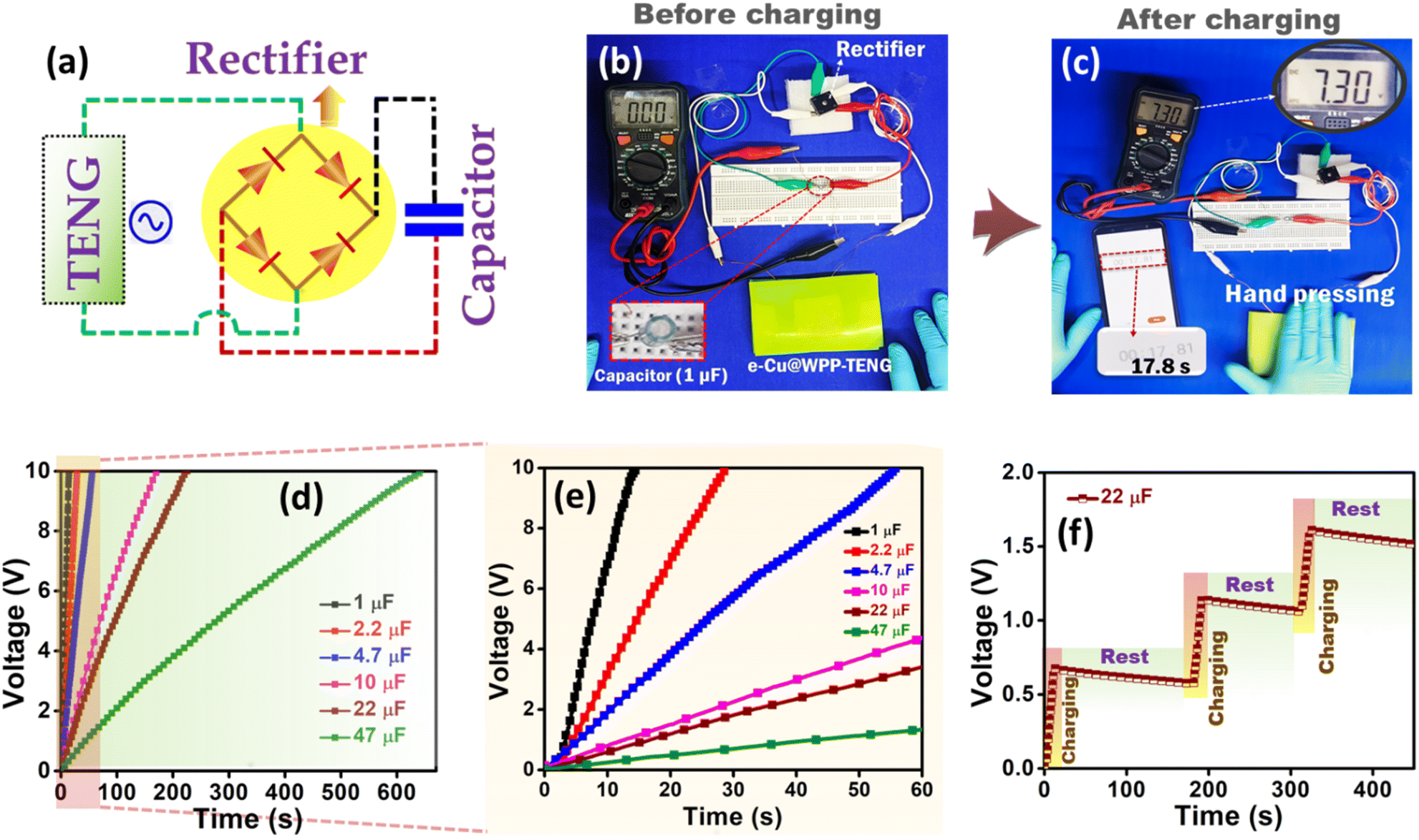 | ||
| Fig. 5 (a) Circuit diagram for charging the capacitor by using e-Cu@WPP-TENG, (b) & (c) digital photographs showing the 1 μF capacitor before and after charging by using e-Cu@WPP-TENG, (d) voltage–time plot showing the charging of different capacitors by using e-Cu@WPP-TENG, (e) zoomed-in portion of (d) showing the charging of capacitors in a 1 minute time period, and (f) voltage–time plot for a 22 μF capacitor with alternating charging and rest periods provided by hand pressing of e-Cu@WPP-TENG. | ||
To demonstrate the practical applicability of e-Cu@WPP-TENG a digital calculator was powered using the hand pressing movements using the electric circuit and experimental setup shown in Fig. 6a and b respectively. The preinstalled button cell was removed from the back of the calculator (Fig. 6c) and power connections were connected to a 22 μF capacitor. The TENG under hand pressing after a few seconds successfully powered on the calculator (Movie S3![[thin space (1/6-em)]](https://www.rsc.org/images/entities/char_2009.gif) † and Fig. 6d–e). First, the capacitor was charged with the help of e-Cu@WPP-TENG. In order to display the perfect working condition of the calculator under a TENG power supply, a simple mathematical calculation was performed as depicted in Fig. 6f. This successfully demonstrates the practical applicability of e-Cu@WPP-TENG for powering electronic devices.
† and Fig. 6d–e). First, the capacitor was charged with the help of e-Cu@WPP-TENG. In order to display the perfect working condition of the calculator under a TENG power supply, a simple mathematical calculation was performed as depicted in Fig. 6f. This successfully demonstrates the practical applicability of e-Cu@WPP-TENG for powering electronic devices.
 | ||
| Fig. 6 (a) Circuit diagram for powering the electronic devices by using e-Cu@WPP-TENG, (b) digital photographs showing the experimental setup for charging a digital calculator by using the TENG, (c) picture showing the back side of the calculator with no external power source, (d) & (e) digital photographs showing the calculator powered on by the hand pressing of e-Cu@WPP-TENG, and (f) digital images showing the working of a calculator powered by e-Cu@WPP-TENG. | ||
The application of this device can be extended to a vast number of utilities. One such application can be to place the e-Cu@WPP-TENG under the parking areas and mats of the door/gate of a hotel, restaurant, building, laboratory, or home to harvest the energy from the pressing movement introduced by the people passing by or any load over it. The energy generated from these mechanical movements can be used to power the various LED panels of advertisements, address boards, logos, nameplates, etc. (Fig. S27†). To power the LED panel, electric circuit shown in Fig. S28a† was utilized to convert the AC output from e-Cu@WPP-TENG to a DC input before supplying it to the LED panel. To replicate the address board of any business, office, or laboratory, 96 green LEDs were connected in series which were powered by hand pressing the e-Cu@WPP-TENG (Fig. S28b, c & Movie S4†). Furthermore, to check the ability of e-Cu@WPP-TENG to power multiple LED lights, 472 LED lights were connected in series to construct a random LED panel (Fig. 7a). Fig. 7a & Movie S5† depict the lighting of the LED panel by hand pressing of e-Cu@WPP-TENG thus backing up the capabilities of TENGs to power LED panels for various advertisement displays. Lastly, to replicate the practical use case scenario for powering the address board of any business, office, or laboratory, an LED panel was installed alongside the door of the laboratory (Fig. 7b). e-Cu@WPP-TENG was placed under the shoe mat in front of the door and was connected to the LED panel through copper wires. As the subject steps over the mat before entering the lab, the pressing movement of their feet triggers the contact-separation in e-Cu@WPP-TENG which is sufficient to illuminate the LED panel as depicted in Movie S6.† Furthermore, the application of the e-Cu@WPP-TENG device was demonstrated to utilize the mechanical energy of a running athlete over a treadmill for harvesting useful energy.
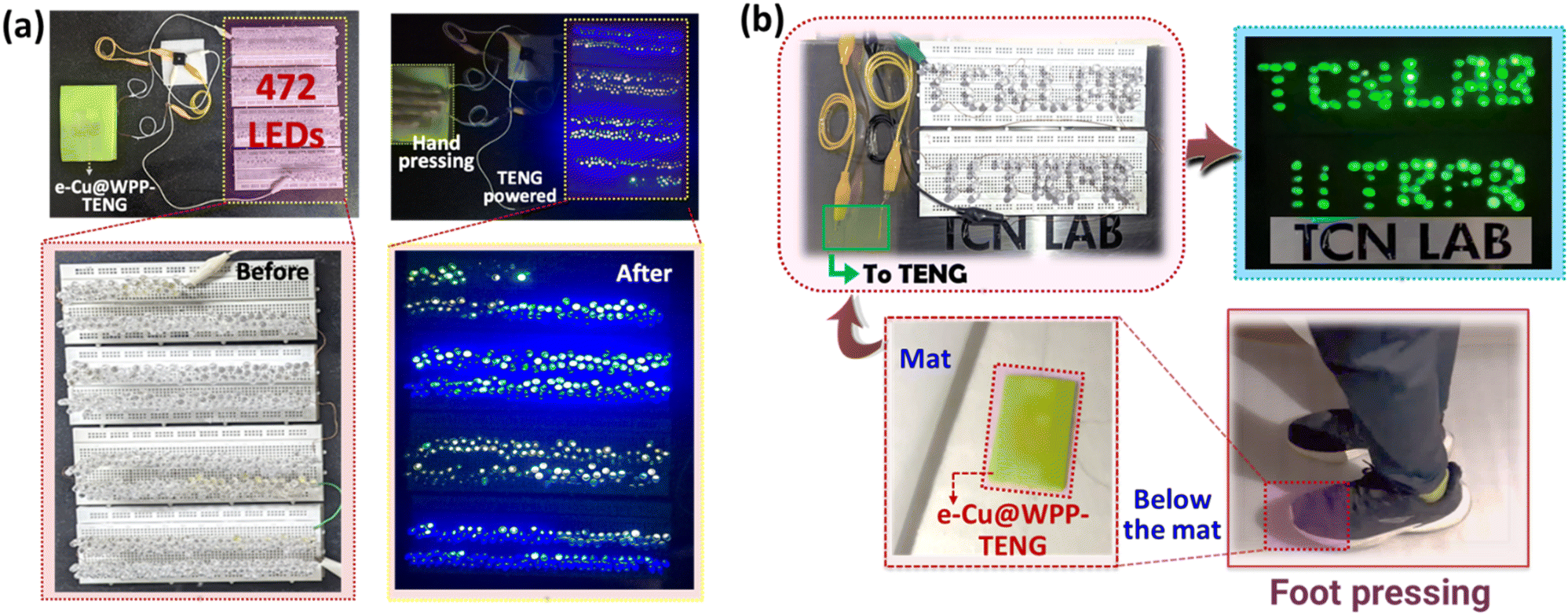 | ||
| Fig. 7 (a) LED panel with 472 LED lights connected in series powered by using e-Cu@WPP-TENG under human hand pressing. (b) LED panel showing the name and address of the laboratory power-driven by foot pressing of e-Cu@WPP-TENG. | ||
A LED panel showing the sign “FITNESS” was connected to the output of the TENG which started to glow when the athlete started running (Fig. S29†). This application serves as a prototype for harvesting energy while helping individuals achieve their fitness goals. These demonstrations showcase the wide application range of e-Cu@WPP-TENG aiming to break into the commercial market by repurposing plastic and economic waste.
Conclusion
Plastic and E-waste are pressing concerns for the modern era which are affecting both human health and the environment. Herein, we have proposed an economically and chemically viable procedure to target both plastic and E-waste management to harvest the mechanical energy from human bodily motions. Waste PET obtained from Kapton tape was used as a tribo-negative material which was paired with normal printing paper as a tribo-positive material to fabricate the TENG. Moreover, simple and economically viable electrodeposition of copper layers over triboelectric materials is reported as a substitute for expensive and sophisticated coating procedures. The fabricated e-Cu@WPP-TENG demonstrated a high open-circuit voltage of ∼552 V and a high peak power density of 7.68 W m−2 under human hand tapping. The reduced interfacial resistance among triboelectric and electrodeposited electrode layers resulted in ∼3 and ∼11 times higher open-circuit voltages than those of Cu-taped and C-coated electrode layers. To demonstrate the practical applicability of e-Cu@WPP-TENG the harvested energy has been stored in commercial capacitors and was utilized to power the electronic devices such as digital calculator. Furthermore, the device could power 472 LEDs connected in series and the demonstration was extended to showcase the application of e-Cu@WPP-TENG to power the LED panels for various advertisements, signboards, or name plates outside hotels, buildings, homes, etc. by feet or load movement near the gate/door. In a nutshell, this work stresses the importance of extracting useful energy from plastic and E-waste and promotes the use of economical and profitable means to harvest energy from human bodily motions.Experimental section
Fabrication of triboelectric and electric layers
Plastic sheets acquired from used Kapton tape and A4 printing paper were first thoroughly cleaned with acetone followed by a thin layer of carbon coating (VC, Vulcan carbon) on one side. Carbon slurry was prepared by mixing VC with polyvinylidene fluoride (PVDF) binder in a 7:3 weight ratio followed by the addition of a suitable amount of N-methyl pyrrolidinone (NMP) solvent. The sacrificial electrodeposition of copper over the carbon-coated plastic and paper sheets (4 cm × 3 cm) was carried out by using damaged electric wires as the anode in 0.05 M CuSO4 electrolyte containing 0.5 M Na2SO4 as the supporting electrolyte (pH maintained ∼3 by using dilute H2SO4) at 1.5 V for 30 minutes. The DC power supply (Aplab regulated DC power supply, L3220) was used for the electrodeposition. The electrodeposited samples were thoroughly rinsed with deionized water and dried in an oven at 60 °C. The final samples were denoted as e-Cu@plastic and e-Cu@paper, wherein the copper-coated side acts as the electrode layer and the other side as a triboelectric layer (plastic as a tribo-negative material and paper as a tribo-positive material).
Fabrication of a triboelectric nanogenerator (e-Cu@WPP-TENG)
The contact-separation design of the triboelectric nanogenerator was prepared by attaching e-Cu@plastic and e-Cu@paper on flexible plastic substrates (procured from an old document folder). The uncoated sides of e-Cu@plastic and e-Cu@paper were made to face each other. To achieve contact and separation between the triboelectric layers, thermocol foam was used as the spacer. The polished copper wires were attached to electrode layers to obtain the output of the triboelectric nanogenerator. The designed triboelectric nanogenerator was abbreviated as e-Cu@WPP-TENG (electrodeposited copper on a waste plastic and paper triboelectric nanogenerator).Working and demonstration of e-CuWPP-TENG
To harvest the electrical energy from e-Cu@WPP TENG, human hand tapping was used to provide mechanical stimulation for vertical contact and separation. The generated electrical outputs were recorded by using an oscilloscope (Keysight InfiniiVision DSOX2024A) and electrometer (Keysight B2987A Electrometer/High Resistance Meter). A rectifier was used to convert the alternating current (AC) outputs from the nanogenerator to direct current (DC). The charging of commercial capacitors of different capacitances was monitored by using a battery cycler (BCS-810, Biologic). As a demonstration of the practical applicability of e-CuWPP-TENG, hand tapping was used as a source of mechanical motions to power 472 LED lights, charge commercial capacitors, and power electronic calculators and LED panels for advertisement/address board. Simulation studies were conducted using FEM (finite element method) based COMSOL Multiphysics software. A 2D model of a TENG was simulated and studies were conducted.Data availability
The data supporting this article have been included as part of the ESI.†Conflicts of interest
There are no conflicts to declare.Acknowledgements
The authors thank the Central Research Facility (CRF), IIT Ropar, for FE-SEM measurements and, Harshith Kumar and Dilbag Singh Dhillon for assistance in the electrical measurements. T. C. Nagaiah thanks the Science and Engineering Research Board (SERB, SCP/2022/000363) for funding. M. Singh thanks IIT Ropar and K. Garg is thankful for the Prime Minister Research Fellowship (PMRF).References
- X. Feng, Q. Li and K. Wang, ACS Appl. Mater. Interfaces, 2021, 13, 400–410 CrossRef CAS PubMed.
- T. Hundertmark, M. Mayer, C. McNally, T. J. Simons, and C. Witte, How Plastics Waste Recycling Could Transform The Chemical Industry, 2023, https://www.mckinsey.com/industries/chemicals/our-insights/how-plastics-waste-recycling-could-transform-the-chemical-industry#, accessed 07-09-2023 Search PubMed.
- I. Vollmer, M. J. F. Jenks, M. C. P. Roelands, R. J. White, T. van Harmelen, P. de Wild, G. P. van der Laan, F. Meirer, J. T. F. Keurentjes and B. M. Weckhuysen, Angew. Chem., Int. Ed., 2020, 59, 15402–15423 CrossRef CAS PubMed.
- H. Zhou, Y. Wang, Y. Ren, Z. Li, X. Kong, M. Shao and H. Duan, ACS Catal., 2022, 12, 9307–9324 CrossRef CAS.
- M. Ashraf, N. Ullah, I. Khan, W. Tremel, S. Ahmad and M. N. Tahir, Chem. Rev., 2023, 123, 4443–4509 CrossRef CAS PubMed.
- S. Kwon, J. Kang, B. Lee, S. Hong, Y. Jeon, M. Bak and S.-k. Im, Energy Environ. Sci., 2023, 16, 3074–3087 RSC.
- L. Li, H. Luo, Z. Shao, H. Zhou, J. Lu, J. Chen, C. Huang, S. Zhang, X. Liu, L. Xia, J. Li, H. Wang and Y. Sun, J. Am. Chem. Soc., 2023, 145, 1847–1854 CrossRef CAS PubMed.
- T. Ren, Z. Duan, H. Wang, H. Yu, K. Deng, Z. Wang, H. Wang, L. Wang and Y. Xu, ACS Catal., 2023, 13, 10394–10404 CrossRef CAS.
- Y. Tang, Z. Cen, Q. Ma, B. Zheng, Z. Cai, S. Liu and D. Wu, Adv. Sci., 2023, 10, 2206924 CrossRef CAS PubMed.
- J. Y. Q. Teo, A. Ong, T. T. Y. Tan, X. Li, X. J. Loh and J. Y. C. Lim, Green Chem., 2022, 24, 6086–6099 RSC.
- B. Kaur, R. K. Gupta and H. Bhunia, Microporous Mesoporous Mater., 2019, 282, 146–158 CrossRef CAS.
- X. Yuan, S. Li, S. Jeon, S. Deng, L. Zhao and K. B. Lee, J. Hazard. Mater., 2020, 399, 123010 CrossRef CAS PubMed.
- C. Ge, J. Song, Z. Qin, J. Wang and W. Fan, ACS Appl. Mater. Interfaces, 2016, 8, 18849–18859 CrossRef CAS PubMed.
- S. Yan, R. Li, X. Fu, W. Yuan, L. Jin, Y. Li, X. Wang and Y. Zhang, Energy Fuels, 2022, 36, 11012–11024 CrossRef CAS.
- V. G. Pol and M. M. Thackeray, Energy Environ. Sci., 2011, 4, 1904–1912 RSC.
- G. Tang, W. Qiao, Z. Wang, F. Liu, L. He, M. Liu, W. Huang, H. Wu and C. Liu, Green Chem., 2023, 25, 3738–3766 RSC.
- J. Xu, S. Dou, W. Zhou, C. Yang, I. Manke, P. Zhang, Z. Yan, Y. Xu, Q. Yuan, Y. Zhang, W. Liu, R. Chen and Y. Chen, Nano Energy, 2022, 95, 107015 CrossRef CAS.
- Y. Chai, M. Wang, N. Gao, Y. Duan and J. Li, Chem. Eng. J., 2020, 396, 125260 CrossRef CAS.
- A. K. Awasthi, J. Li, L. Koh and O. A. Ogunseitan, Nat. Electron., 2019, 2, 86–89 CrossRef.
- M. U. Bukhari, A. Khan, K. Q. Maqbool, A. Arshad, K. Riaz and A. Bermak, Energy Rep., 2022, 8, 1687–1695 CrossRef.
- R. F. S. M. Ahmed, S. Amini, S. M. Ankanathappa and K. Sannathammegowda, Waste Manage., 2024, 178, 1–11 CrossRef PubMed.
- N. R. Chodankar, S.-H. Ji, Y.-K. Han and D.-H. Kim, Nano-Micro Lett., 2019, 12, 1 Search PubMed.
- H. Kumar, S. Kumagai, T. Kameda, Y. Saito and T. Yoshioka, React. Chem. Eng., 2020, 5, 1805–1813 RSC.
- F.-R. Fan, Z.-Q. Tian and Z. Lin Wang, Nano Energy, 2012, 1, 328–334 CrossRef CAS.
- D. Choi, Y. Lee, Z.-H. Lin, S. Cho, M. Kim, C. K. Ao, S. Soh, C. Sohn, C. K. Jeong, J. Lee, M. Lee, S. Lee, J. Ryu, P. Parashar, Y. Cho, J. Ahn, I.-D. Kim, F. Jiang, P. S. Lee, G. Khandelwal, S.-J. Kim, H. S. Kim, H.-C. Song, M. Kim, J. Nah, W. Kim, H. G. Menge, Y. T. Park, W. Xu, J. Hao, H. Park, J.-H. Lee, D.-M. Lee, S.-W. Kim, J. Y. Park, H. Zhang, Y. Zi, R. Guo, J. Cheng, Z. Yang, Y. Xie, S. Lee, J. Chung, I.-K. Oh, J.-S. Kim, T. Cheng, Q. Gao, G. Cheng, G. Gu, M. Shim, J. Jung, C. Yun, C. Zhang, G. Liu, Y. Chen, S. Kim, X. Chen, J. Hu, X. Pu, Z. H. Guo, X. Wang, J. Chen, X. Xiao, X. Xie, M. Jarin, H. Zhang, Y.-C. Lai, T. He, H. Kim, I. Park, J. Ahn, N. D. Huynh, Y. Yang, Z. L. Wang, J. M. Baik and D. Choi, ACS Nano, 2023, 17, 11087–11219 CrossRef CAS PubMed.
- H. Zou, Y. Zhang, L. Guo, P. Wang, X. He, G. Dai, H. Zheng, C. Chen, A. C. Wang, C. Xu and Z. L. Wang, Nat. Commun., 2019, 10, 1427 CrossRef PubMed.
- T. Li, Y. Xu, M. Willander, F. Xing, X. Cao, N. Wang and Z. L. Wang, Adv. Funct. Mater., 2016, 26, 4370–4376 CrossRef CAS.
- B. Zhang, Y. Tang, R. Dai, H. Wang, X. Sun, C. Qin, Z. Pan, E. Liang and Y. Mao, Nano Energy, 2019, 64, 103953 CrossRef CAS.
- Q. M. Saqib, M. Y. Chougale, M. U. Khan, R. A. Shaukat, J. Kim, J. Bae, H. W. Lee, J.-I. Park, M. S. Kim and B. G. Lee, Nano Energy, 2021, 89, 106458 CrossRef CAS.
- R. Ouyang, Y. Huang, H. Ye, Z. Zhang and H. Xue, Nano Energy, 2022, 102, 107749 CrossRef CAS.
- Z. Song, W. Li, H. Kong, Y. Bao, N. Wang, W. Wang, Y. Ma, Y. He, S. Gan and L. Niu, Nano Energy, 2022, 92, 106759 CrossRef CAS.
- T. Bhatta, S. Sharma, K. Shrestha, Y. Shin, S. Seonu, S. Lee, D. Kim, M. Sharifuzzaman, S. M. S. Rana and J. Y. Park, Adv. Funct. Mater., 2022, 32, 2202145 CrossRef CAS.
- S. Roy, P. K. Maji and K.-L. Goh, Chem. Eng. J., 2021, 413, 127409 CrossRef CAS.
- X. Fan, J. Chen, J. Yang, P. Bai, Z. Li and Z. L. Wang, ACS Nano, 2015, 9, 4236–4243 CrossRef CAS PubMed.
- Y. Feng, Y. Zheng, Z. U. Rahman, D. Wang, F. Zhou and W. Liu, J. Mater. Chem. A, 2016, 4, 18022–18030 RSC.
- S. Chen, J. Jiang, F. Xu and S. Gong, Nano Energy, 2019, 61, 69–77 CrossRef CAS.
- K. Shi, H. Zou, B. Sun, P. Jiang, J. He and X. Huang, Adv. Funct. Mater., 2020, 30, 1904536 CrossRef CAS.
- F. Wang, S. Wang, Y. Liu, S. Ouyang, D. Sun, X. Yang, J. Li, Z. Wu, J. Qian, Z. Zhao, L. Wang, C. Jia and S. Ma, Nano Lett., 2024, 24, 2861–2869 CrossRef CAS PubMed.
- J. T. Li, M. G. Stanford, W. Chen, S. E. Presutti and J. M. Tour, ACS Nano, 2020, 14, 7911–7919 CrossRef CAS PubMed.
- S. Cho, Y. Shin, J. Choi, J. Eom, B. S. Oh, J. Lee and G. Y. Jung, Nano Energy, 2020, 77, 105184 CrossRef CAS.
- S. M. Nawaz, M. Saha, N. Sepay and A. Mallik, Nano Energy, 2022, 104, 107902 CrossRef CAS.
- K. K. Jena, B. Fatma, S. S. Arya, S. M. Alhassan, V. Chan, A. M. Pappa and C. Pitsalidis, J. Mater. Chem. A, 2024, 12, 8340–8349 RSC.
- H. S. Wang, C. K. Jeong, M.-H. Seo, D. J. Joe, J. H. Han, J.-B. Yoon and K. J. Lee, Nano Energy, 2017, 35, 415–423 CrossRef CAS.
- H. Chen, L. Bai, T. Li, C. Zhao, J. Zhang, N. Zhang, G. Song, Q. Gan and Y. Xu, Nano Energy, 2018, 46, 73–80 CrossRef CAS.
- M. Lai, B. Du, H. Guo, Y. Xi, H. Yang, C. Hu, J. Wang and Z. L. Wang, ACS Appl. Mater. Interfaces, 2018, 10, 2158–2165 CrossRef CAS PubMed.
- H. Chen, S. Zhang, Y. Zou, C. Zhang, B. Zheng, C. Huang, B. Zhang, C. Xing, Y. Xu and J. Wang, ACS Appl. Electron. Mater., 2020, 2, 1106–1112 CrossRef CAS.
- S. S. H. Abir, M. U. K. Sadaf, S. K. Saha, A. Touhami, K. Lozano and M. J. Uddin, ACS Appl. Mater. Interfaces, 2021, 13, 60401–60412 CrossRef CAS PubMed.
- Y. A. Stetsiv, M. M. Yatsyshyn, D. Nykypanchuk, S. A. Korniy, I. Saldan, O. V. Reshetnyak and T. J. Bednarchuk, Polym. Bull., 2021, 78, 6251–6265 CrossRef CAS.
- S. G. Prasad, A. De and U. De, Int. J. Spectrosc., 2011, 2011, 810936 CrossRef.
- R. Zhang and H. Olin, EcoMat, 2020, 2, e12062 CrossRef CAS.
- R. Mao, D. Zhang, Z. Wang, H. Zhang, D. Wang, M. Tang, L. Zhou, H. Cai and H. Xia, Nano Energy, 2023, 111, 108418 CrossRef CAS.
- M. Sahu, S. Hajra, S. Panda, M. Rajaitha, B. K. Panigrahi, H.-G. Rubahn, Y. K. Mishra and H. J. Kim, Nano Energy, 2022, 97, 107208 CrossRef CAS.
- G. Zhu, C. Pan, W. Guo, C.-Y. Chen, Y. Zhou, R. Yu and Z. L. Wang, Nano Lett., 2012, 12, 4960–4965 CrossRef CAS PubMed.
- S. Niu and Z. L. Wang, Nano Energy, 2015, 14, 161–192 CrossRef CAS.
- G. S. P. Castle, J. Electrost., 1997, 40–41, 13–20 CrossRef.
- J. F. Hughes, Phys. Bull., 1987, 38, 424 CrossRef.
- W.-G. Kim, D.-W. Kim, I.-W. Tcho, J.-K. Kim, M.-S. Kim and Y.-K. Choi, ACS Nano, 2021, 15, 258–287 CrossRef CAS PubMed.
- L.-H. Lee, J. Electrost., 1994, 32, 1–29 CrossRef CAS.
- P. Keith Watson and Z.-Z. Yu, J. Electrost., 1997, 40–41, 67–72 CrossRef.
- F. Saurenbach, D. Wollmann, B. Terris and A. J. L. Diaz, Langmuir, 1992, 8, 1199–1203 CrossRef CAS.
- S. Niu, Y. Liu, S. Wang, L. Lin, Y. S. Zhou, Y. Hu and Z. L. Wang, Adv. Mater., 2013, 25, 6184–6193 CrossRef CAS PubMed.
Footnotes |
| † Electronic supplementary information (ESI) available. See DOI: https://doi.org/10.1039/d4ta07070d |
| ‡ These authors contributed equally. |
| This journal is © The Royal Society of Chemistry 2025 |