
 Open Access Article
 This Open Access Article is licensed under a
 Creative Commons Attribution 3.0 Unported Licence
Roll-to-roll slot-die coating of PTAA with PEDOT:PSS buffer layer for perovskite solar cells: coating analysis by XPS mapping†
Rahul
Patidar
 *,
James
McGettrick
,
Rodrigo
Garcia-Rodriguez
,
Chris
Griffiths
,
Kathryn
Lacey
,
Ershad
Parvazian
,
David
Beynon
,
Matthew
Davies
and
Trystan
Watson
*
*,
James
McGettrick
,
Rodrigo
Garcia-Rodriguez
,
Chris
Griffiths
,
Kathryn
Lacey
,
Ershad
Parvazian
,
David
Beynon
,
Matthew
Davies
and
Trystan
Watson
*
SPECIFIC IKC, Faculty of Science and Engineering, Swansea University, Fabian Way, Swansea SA1 8EN, UK. E-mail: t.m.watson@swansea.ac.uk; ra.patidar12@gmail.com
First published on 20th March 2025
Abstract
Roll-to-Roll (R2R) deposition offers a promising route for scaling up the production of perovskite solar cells (PSCs); however, the performance of R2R-fabricated devices still lags behind those produced through laboratory-scale methods. One significant factor contributing to this performance gap, particularly in P–I–N structured devices, is the use of suboptimal hole transport layers (HTLs), such as poly(3,4-ethylenedioxythiophene)–polystyrenesulfonate (PEDOT:PSS). In this study, we explore the potential of replacing PEDOT:PSS with poly[bis(4-phenyl)(2,4,6-trimethylphenyl)amine] (PTAA), a more efficient and stable HTL. While undoped PTAA alone shows promise, its application on the rough surface of PET-ITO substrates is insufficient to fully replace PEDOT:PSS, leading to reduced device performance. However, when combined with a PEDOT:PSS buffer layer, PTAA demonstrated significant improvements, achieving a power conversion efficiency (PCE) of 15.2% compared to 12.6% with PTAA alone using R2R deposition. To better understand the coating characteristics and interactions of these materials, we conducted a detailed analysis of the surface topography of PET-ITO and the HTL layer using X-ray photoelectron spectroscopy (XPS) mapping. This study provides critical insights into the synergistic effects of PEDOT:PSS and PTAA, highlighting their combined potential for enhancing the efficiency of R2R-fabricated PSCs.
Introduction
The pursuit of scalable and efficient manufacturing techniques for perovskite solar cells (PSCs) has been driven by the need to optimise both processability and performance.1,2 Among the various methods explored, Roll-to-Roll (R2R) deposition has emerged as a promising approach for large-scale production.3–6 Our previous work concentrated on devising a scalable method for Roll-to-Roll (R2R) deposition of P–I–N PSCs through a four-layer slot-die coating process.7 However, the performance of R2R-fabricated P–I–N PSCs8–11 continues to fall short of the high Power Conversion Efficiencies (PCE) exceeding 20% on flexible substrates achieved by laboratory-scale methods.12,13 One factor contributing to this reduced performance via R2R is the typical use of poly(3,4-ethylenedioxythiophene)–polystyrene sulfonate (PEDOT:PSS) as a Hole Transport Layer (HTL) in P–I–N PSCs.7,8,14,15 Although PEDOT:PSS is widely used because of its ease of deposition16,17 and high conductivity, it inadvertently hampers device performance by increasing the interfacial recombination at the PEDOT/perovskite interface.18,19 Additionally, the acidic nature of PSS can degrade the interface, further compromising the longevity of PSCs.20 This study aims to address these challenges by exploring alternative HTL such as poly[bis(4-phenyl)(2,4,6-trimethylphenyl)amine] (PTAA) that can better balance the demands of scalable manufacturing with high efficiency and durability.PTAA is a conjugated, high-performance hole transport material widely used in various optoelectronic devices, such as organic light-emitting diodes (OLEDs)21 and perovskite solar cells (PSCs).22 PTAA is of particular interest in the field of PSCs due to its promising properties. Its highest occupied molecular orbital (HOMO) energy level is well-matched with the valence band of MAPbI3, leading to efficient hole extraction and reduced energy loss.23 However, PTAA exhibits low hole mobility,24 as a result, it is typically deposited as a very thin layer, usually in the range of 10 nm, to minimise series resistance and higher-order nonradiative recombination losses.25 Furthermore, PTAA exhibits excellent environmental stability due to its hydrophobicity, which can contribute to the durability of the PSCs.26 It is also air-stable, which allows it to be coated in ambient conditions, potentially reducing the fabrication complexity and costs of devices.23 It's also important to note that PTAA has a high resistance to mechanical stress,27 which makes it an ideal choice for flexible PSCs where the devices are expected to withstand bending or folding without degrading their performance.
PTAA, when used as a HTL in P–I–N PSCs, is commonly used as a very thin layer in the range of 10 nm to eliminate series resistance losses as well as higher-order non-radiative recombination losses.18 This presents a challenge for large-scale, roll-to-roll fabrication processes due to the difficulty of depositing such thin layers uniformly over large areas. This is particularly a problem for flexible substrates due to the high roughness of ITO on PET films. To circumvent this, we explored the use of PEDOT:PSS as a ‘buffer layer’ rather than as an HTL. The buffer layer will be used to achieve good ITO coverage while PTAA will help with effective charge extraction. The aim of this approach is to leverage the strengths of both PEDOT:PSS and PTAA, to increase shunt resistance, improve charge extraction, and mitigate potential device instability, thereby enhancing overall performance.28 PEDOT:PSS tends to form uniform films and unlike PTAA, the thickness of PEDOT:PSS films does not contribute to a significant increase in the device's series resistance, thanks to the conductive properties inherent to PEDOT:PSS. This bilayer architecture facilitates the coating of the PTAA layer with reduced thickness while achieving excellent ITO coverage, achieving a power conversion efficiency (PCE) of 15.2%, compared to 12.6% with PTAA alone. To gain insights into the coating behaviour of the HTL and buffer layer over a large area relevant to manufacturing-scale applications, we conducted a detailed analysis using X-ray Photoelectron Spectroscopy (XPS) mapping. In the following sections, we present a comprehensive examination of the buffer layer and HTL, emphasizing their role in effective ITO coverage for efficient PSC performance and their scalability through the R2R slot-die coating process.
Results and discussion
Incorporating an ultrathin layer of undoped PTAA, achieved by spin-coating a 2.5 mg per ml PTAA solution onto a glass substrate, resulted in excellent performance in PSCs with hero PCE of over 17% (a box plot illustrating between 1 mg ml−1 and 3 mg ml−1 is shown in Fig. S1†). Although accurately determining the thickness of the PTAA layer from the 2.5 mg ml−1 solution was challenging, we estimate the layer to be less than 20 nm thick, based on measurements of a PTAA layer deposited from a 5 mg per mL solution, which yielded a thickness of 32 nm. In this study, the concentration of the coated formulation is used as a proxy for the dry PTAA thickness, as it proves difficult to directly measure ultrathin PTAA films particularly on flexible substrates.When the same 2.5 mg per ml PTAA concentration is applied to flexible polymer substrate (PET-ITO), a significant decrease in performance is observed, with many devices exhibiting near-zero PCE. However, coating with a higher PTAA concentration (5 mg ml−1) resulted in improved performance compared to devices utilizing a lower PTAA concentration (2.5 mg ml−1), a box plot comparing glass and flexible PET is shown in Fig. S2.† This implies that the coverage of ITO is likely insufficient when using the 2.5 mg per mL PTAA solution, leading to reduced device efficiency. To investigate the underlying cause of this performance variation, we characterised glass-ITO and PET-ITO substrates using atomic force microscopy (AFM). The results are presented in Fig. 1, as expected the glass-ITO substrate is significantly smoother compared to the PET-ITO substrate. Prominent spikes ranging from 20 to 40 nm on the PET-ITO substrate likely contact the perovskite layer when the PTAA film thickness is below 20 nm, inducing interfacial recombination and thus reducing the overall performance of the PSCs. These morphological differences in ITO are attributed to the structural and morphological changes imposed by the polymer substrates during crystal formation.29
 | ||
| Fig. 1 (a) 2D and 3D topography of glass ITO and (b) PET-ITO. | ||
A straightforward approach to address this issue as described previously is to apply a thicker layer of PTAA to completely cover the ITO surface, in this case achieved by increasing the PTAA concentration from 2.5 mg ml−1 to 5 mg ml−1. To effectively mask the 40 nm ITO spikes, a PTAA layer of at least 40 nm would be necessary. However, PTAA is known for its high resistivity and low hole mobility, and increasing its thickness introduces additional series resistance and higher-order non-radiative recombination losses.18,30 To overcome this, incorporation of dopants such as F4-TCNQ, LiTFSI, and tBP into PTAA for efficient P–I–N PSCs have been extensively explored.31–33 Although doping helps improve PCEs, it presents its own set of challenges, including aggregation34 and degradation35 of interfaces over time which is not ideal for scale up applications. Therefore, we adopted a different approach by incorporating a PEDOT:PSS buffer layer to effectively cover the ITO spikes, followed by a thin PTAA layer to efficiently extract holes from the active layer.
To assess the extent and consistency of ITO coverage with and without the PEDOT:PSS buffer layer, XPS analysis was conducted on three different film configurations: (i) PET-ITO-PEDOT:PSS (hereafter referred to as PEDOT:PSS), (ii) PET-ITO-PTAA (hereafter referred to as PTAA), and (iii) PET-ITO-PEDOT:PSS-PTAA (hereafter referred to as PEDOT:PSS-PTAA). High-resolution spectra were analysed to determine the elemental composition and chemical states of the deposited layers. The surface composition in atomic% for all three layers is presented in Table S3.†
The XPS spectra of PEDOT:PSS films (Fig. S4†) confirmed the presence of expected elements, including carbon (C), oxygen (O), and sulfur (S), which are characteristic of PEDOT and PSS. The sulfur content, derived from both the thiophene units in PEDOT and the sulfonate groups in PSS, was measured at 6.5 at%, which is slightly lower than the theoretical values expected for pure PEDOT (11.1 at%) or PSS (8.3 at%). This deviation is partly due to the presence of ITO in the analysis volume, but also suggests other components are present, including a low concentration of a high-binding energy nitrogen species at 401.9 eV, either as deliberate commercial additives or the expected adventitious carbon.
For PTAA films (Fig. S5†), the XPS spectra exhibited a distinct N(1s) peak at 400.1 eV, confirming the incorporation of nitrogen from the PTAA molecular structure. Additionally, the C(1s) peak was observed at 284.9 eV, a binding energy typically associated with C–C bonds. However, in this case, the slight shift in binding energy may indicate surface charging effects, which are commonly observed in relatively thick and poorly conductive polymer films. As expected, no sulfur signal (S(2p)) was detected in the PTAA layer.
In the case of the PEDOT:PSS-PTAA bilayer films (Fig. S6†), the spectra were dominated by the overlying PTAA layer, as evidenced by the prominent N(1s) peak at 399.6 eV. Notably, a secondary, lower-intensity peak centred at 401.4 eV was also detected, suggesting the presence of a chemically oxidised nitrogen species, such as a quaternary amine, is a component of the underlying PEDOT:PSS (Fig. S4†). For a more detailed analysis of the XPS spectra, please refer to the ESI document.
Although PEDOT:PSS and PTAA are intended to fully coat the ITO surface, the detection of In(3d) at 445.0 eV in both the films indicates that portions of the ITO substrate remained exposed or that the film thickness in certain areas was below the XPS sampling depth (<10 nm), allowing signal contribution from the underlying indium. However, in the PEDOT:PSS-PTAA bilayer, the indium signal was significantly reduced, suggesting that the combination of PEDOT:PSS and PTAA provided enhanced ITO coverage compared to the individual layers.
In order to understand the consistency and get more insight over a larger area, we scanned an area measuring 25.5 mm × 8.25 mm, where we recorded a set of spectra at each point. To assess any changes in the peak shift we show the raw spectra (Fig. S7†) from 210 points on PEDOT:PSS-PTAA films. No significant chemical shifts in the XPS peaks of the spectra were observed across all the points. We then calculated the atomic percentage of indium (In), sulfur (S), and nitrogen (N) for PEDOT:PSS, PTAA, and PEDOT:PSS-PTAA. 2D intensity maps from the scans, are shown in Fig. 2a. The scales in the individual maps are adjusted to reflect the minimum and maximum intensity values specific to each corresponding map.
 | ||
| Fig. 2 (a) XPS atomic% map of R2R slot-die coated PEDOT:PSS (0.77% mean In, 6.2% mean S), PTAA (3.03% mean In, 2.83% mean N), PEDOT:PSS-PTAA (0.05% mean In, 0.47% mean S) on PET ITO. (b) Variation of S against In in slot die coated PEDOT:PSS on PET-ITO. (c) Variation of N against In in slot die coated PTAA on PET-ITO. | ||
The detection of sulfur across the coated area in the intensity map of the PEDOT:PSS substrate confirmed the presence of PEDOT:PSS and served as a proxy to probe the uniformity of the PEDOT:PSS buffer layer. The sulfur percentage used for constructing the sulfur map accounted for both sulphonate from PSS and thiophene from PEDOT, with a constant ratio between the PEDOT and PSS components across the mapped points. The uniform sulfur signal observed across the mapped area signifies a consistent presence of PEDOT:PSS on the ITO surface across the mapped area. Conversely, the indium map reveals non-uniformity in the distribution of indium detected under the PEDOT:PSS layer. As the typical sampling depth of XPS is just 10 nm, the presence of indium in the spectra could mean two possible scenarios: (1) the dry film thickness of PEDOT:PSS is close to 10 nm, allowing the underlying ITO to contribute to the detected signal, or (2) defects or pinholes in the PEDOT:PSS layer expose areas of the ITO substrate. If the later were true and PEDOT:PSS layer were not uniformly coated, we would expect an inverse relationship between indium and sulfur intensities i.e., regions with high indium detection should exhibit relatively low sulfur detection due to exposed ITO. To investigate this relationship, we plotted the sulfur and indium intensities from the XPS mapping data as a 2D scatter plot (Fig. 2b), with indium on the Y-axis and sulfur on the X-axis. Interestingly, the scatter plot does not reveal a strong correlation between the presence of indium from the substrate and sulfur from the PEDOT:PSS coating. Instead, the data points are clustered in the same region without following a clear trend. These findings suggest that widespread pinholes in the PEDOT:PSS layer are unlikely. This suggests either the PEDOT:PSS layer forms a continuous film over the ITO, but with localised variations in thickness—particularly <10 nm, allowing partial signal contribution from the underlying ITO (less likely), or the coating consists of a heterogeneous distribution of fully covered and exposed ITO regions. Given that the XPS spot size (300 μm × 700 μm) which is significantly larger than the resolution of AFM, the XPS data provide only a macroscopic perspective, capturing an averaged response rather than resolving finer nanoscale features. Consequently, it's very likely that the observed indium signal could arise from a combination of areas with complete coverage with thickness variation and small pinholes.
By contrast, a PTAA layer coated on top of PET-ITO without a buffer layer of PEDOT:PSS showed significantly high amount of indium (mean 3.03%) compared to the PEDOT:PSS map (mean In 0.77%). This difference is likely coming from the difference in thickness between the two layers, with PTAA being thinner and again within the range of the XPS sampling depth of <10 nm. Unlike the S map of PEDOT:PSS, the distribution of N in PTAA (used as a proxy to the presence of PTAA) was found to be non-uniform across the mapped area of PTAA. To further investigate the relationship between In and N, we present a scatter plot of indium versus nitrogen in Fig. 2c. This revealed the expected distinct inverse correlation pattern consistent with either a thin (<10 nm) or incomplete coating with large pin holes in contrast to the indium–sulfur map of PEDOT:PSS. Poor performance of thin PTAA in a complete device suggest that latter is more likely scenario.
Subsequently, we analysed the maps of the combination of PEDOT:PSS and PTAA layers. The average detected indium percentage was found to be 0.05%, which is approaching the detection limit for XPS and indicates that near-complete coverage of the ITO layer was achieved with the bilayer structure. Interestingly, in the ITO-PEDOT:PSS-PTAA elemental maps, we observed distinct anomalies in both the indium and sulfur distributions (marked by dotted circles in Fig. 2a), whereas no such feature appeared in the nitrogen map (Fig. S8†). These anomalies showed significantly higher intensities of indium and sulfur—but not nitrogen—relative to their respective average intensities. This observation could support the notion that the PEDOT:PSS layer conforms to the underlying topography of the ITO surface, whereas PTAA exhibits a more independent film formation behaviour. However, this evidence alone is not sufficient to definitively confirm this hypothesis, and additional complementary characterisation techniques would be required for a more conclusive assessment which is beyond the scope of this work.
To further understand the behaviour of PEDOT:PSS and PTAA coatings on ITO, we conducted AFM analysis on the same films. We compared the results to interpret changes in morphology and surface roughness. Fig. 3 shows 2 × 2 μm2 maps of the optimised PEDOT:PSS film, PTAA film, and the PEDOT:PSS-PTAA bilayer in conjunction with the PET-ITO substrate. Clear changes in substrate morphology were observed following the deposition of PEDOT:PSS and PTAA. The distinct grains of ITO, which were prominent prior to deposition, became less defined and blurred. We compared the root mean square (RMS) roughness of the four substrates, as shown in Fig. 3. Intriguingly, the deposition of PEDOT:PSS did not significantly alter the roughness of the ITO layer. However, the surface roughness noticeably improved following the deposition of PTAA atop the PET-ITO and PEDOT:PSS layers. When PTAA was directly deposited on the ITO layer, it formed a layer with an average RMS roughness of 0.45 nm. In contrast, when PTAA was deposited on the ITO-PEDOT:PSS bilayer, the roughness was comparable at 0.52 nm. This suggests that while PEDOT:PSS does not substantially alter the inherent roughness of the ITO surface, the PTAA layer plays a crucial role in smoothing the underlying substrate, contributing to a more uniform and refined surface morphology. When looked together with the observed anomalies in PEDOT:PSS-PTAA elemental maps in Fig. 2a, these findings, though supporting the hypothesis that PEDOT:PSS conforms to the morphology of ITO while PTAA functions as a planarisation layer, remain inconclusive due to the vastly different scales used in AFM and XPS. To further investigate, we analysed larger AFM scans (10 μm × 10 μm, Fig. S9†) and observed a consistent trend: PEDOT:PSS does not affect the surface roughness of ITO, whereas PTAA does.
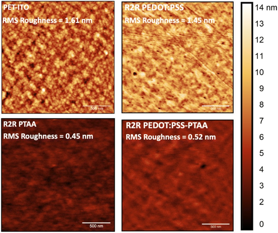 | ||
| Fig. 3 AFM images (2 μm × 2 μm) of ITO-PET, as optimised R2R deposited PEDOT:PSS on ITO-PET, as optimised PTAA deposited on ITO-PET, as optimised PEDOT:PSS-PTAA deposited on ITO-PET. | ||
Moving on to the complete devices, to ascertain the ideal thickness of PEDOT:PSS needed to achieve functioning flexible devices with the equivalent coating thickness of PTAA as applied on glass-ITO substrates, we R2R slot die coated PEDOT:PSS on ITO-PET films with variable wet film thickness. The remaining layers of the architecture PET-ITO-PEDOT:PSS-PTAA-MAPbI3-PCBM-BCP-Ag were spin-coated following the standard procedure of glass-ITO devices to maintain consistent thickness and other parameters. J–V measurements (Fig. S10†) upon completion of the devices showed the optimal wet film thickness of PEDOT:PSS to be 8 μm. We then used this as a standard thickness to optimise the PTAA thickness by R2R slot die coating. Following a similar approach, we determined the optimal PTAA wet film thickness for best-performing PSCs to be 10 μm (Fig. S11†).
Scanning electron microscopy (SEM) imaging of MAPbI3 layers deposited on PET-ITO-PTAA and PET-ITO-PEDOT:PSS-PTAA R2R deposited substrates revealed no significant morphological differences (Fig. 4a). Both substrates exhibited similar crystal sizes and film uniformity. This observation suggests that the presence of the PEDOT:PSS buffer layer did not affect the morphology of the MAPbI3 films, likely due to the effective coverage of PEDOT:PSS by PTAA. The adequate coverage of PEDOT:PSS ensures that its surface energy does not influence the nucleation and grain growth of MAPbI3 films, resulting in similar crystal sizes and film uniformity as observed in the PTAA-only substrates. Furthermore, photoluminescence (PL) measurements (Fig. 4b) indicate a significant quenching of the MAPbI3 PL intensity when a buffer layer of PEDOT:PSS was used compared to the case of a PTAA-only layer. This observation suggests that the introduction of the buffer layer enhanced hole extraction capabilities compared to the single PTAA layer.36
 | ||
| Fig. 4 (a) SEM images of MAPbI3 films coated on PTAA-MAPbI3vs. PTAA-PEDOT:PSS-MAPbI3 (b) PL spectra of MAPbI3 films coated on PTAA-MAPbI3 and PTAA-PEDOT:PSS-MAPbI3 compared with MAPbI3 coated on bare PET-ITO. (c) EL (d) EQE (e) light intensity dependent Voc measurement (f) JV of devices with and without buffer layer of PEDOT:PSS. | ||
Electroluminescence (EL) measurements on complete devices, conducted at an applied voltage of 1.2 V, revealed markedly reduced emission from PTAA-only device (Fig. 4c). The PTAA-only device showed significantly reduced emission, indicating the presence of higher levels of non-radiative recombination and/or lower charge injection to the perovskite layer from the HTL.37 As the only interface that differed in this comparative analysis was the one between the ITO and HTL, it is highly likely that the decrease in emission primarily occurs due to non-radiative recombination at this interface, thereby reducing the Voc of the device. Moreover, external quantum efficiency (EQE) spectra comparison (Fig. 4d) showed a minor reduction in quantum efficiency at shorter wavelengths for devices without PEDOT:PSS, indicating a loss of carriers at the HTL/perovskite interface. The loss of performance due to non-radiative recombination was further validated by conducting light intensity-dependent Voc measurements to calculate the ideality factor of the device (Fig. 4e). The device with PEDOT:PSS as a buffer layer exhibited an ideality factor of 1.09, as determined by the slope of the linear fit, whereas the PTAA-only device showed an ideality factor of 1.44, suggesting a high level of trap-assisted first-order non-radiative recombination.19 Collectively, these findings indicate that the buffer layer of PEDOT:PSS helps reduce non-radiative recombination at the HTL/MAPbI3 interface, resulting in efficient hole extraction compared to PTAA-only devices. This resulted in an overall improvement of the PSC performance. The hero device with the PEDOT:PSS buffer layer achieved a 15.2% power conversion efficiency (PCE) with a short-circuit current density (Jsc) of 20.7 mA cm−2, open-circuit voltage (Voc) of 1.07 V, and fill factor (FF) of 69.26%. In comparison, the PTAA-only device achieved a 12.6% PCE with 19.94 mA cm−2Jsc, 1 V Voc, and 63.39% FF. The respective J–V curves are presented in Fig. 4f, and a statistical comparison of the batch of devices is provided in Fig. S12.† Additionally, the calculated Jsc values based on EQE were 19.27 mA cm−2 with PEDOT:PSS and 18.95 mA cm−2 without PEDOT:PSS. These values are consistent with those obtained from the J–V measurements, suggesting the accuracy of the J–V measurement method.
Conclusions
In conclusion, this study focused on enhancing the performance of R2R coated PSCs by using undoped PTAA as an HTL. To overcome the challenge of depositing thin and uniform PTAA layers on the rough PET-ITO substrate, a buffer layer of PEDOT:PSS was introduced. This approach aimed to leverage the strengths of both materials, improving device performance by reducing recombination and enhancing charge extraction. XPS mapping together with AFM analysis confirmed the different behaviour of PEDOT:PSS and PTAA coatings on PET-ITO. PEDOT:PSS was effective in covering the ITO while PTAA planarised the surface and played a role of more efficient HTL material. The bilayer architecture demonstrated near-complete coverage of the ITO layer, avoiding direct contact with perovskite. The effectiveness of this architecture was confirmed by numeration characterisation such as EL, PL and EQE. The JV measurement resulted in an PCE of 15.2% PCE compared to 12.6% PCE when no buffer layer is used.In conclusion, this research presents an advancement in the field of flexible perovskite photovoltaics. By carefully engineering the HTL interface through the incorporation of a PEDOT:PSS buffer layer, we have developed an optimised device architecture that addresses key challenges in R2R manufacturing of PSCs. This approach not only enhances device efficiency but also paves the way for scalable, high-performance perovskite solar cells. Future work could focus on further optimizing this bilayer structure, exploring its long-term stability, and investigating its applicability to a wider range of perovskite compositions and device architectures. Ultimately, this study contributes valuable insights to the ongoing efforts to bring perovskite solar technology closer to commercial viability.
Data availability
The datasets generated and/or analysed during the current study are available from the corresponding author on request. ESI,† including detailed methodologies and analytical tools, is provided in the ESI text of this paper.† Requests for access to these datasets should be addressed to E-mail: rahul.patidar@swansea.ac.uk.Author contributions
Dr Rahul Patidar conceptualised the study, designed the experiments, and was responsible for all aspects of device fabrication. Dr James McGettrick assisted with XPS experiments and played a significant role in data analysis. Dr Rodrigo Garcia-Rodriguez contributed to EL testing and also participated in data analysis. Dr Chris Griffiths supported the study by conducting AFM measurements and helped with data interpretation. Kathryn Lacey, Dr Ershad Parvazian, and Dr David Beynon were instrumental in various stages of the experimentation process and provided assistance in manuscript preparation. Prof. Matthew Davies and Prof. Trystan Watson supervised the overall project, providing strategic guidance and oversight. All authors reviewed and approved the final manuscript.Conflicts of interest
The authors declare no conflict and all the data is available upon request from the author.Acknowledgements
This work was supported by the VIPERLAB project, funded by the European Union's Horizon 2020 research and innovation programme under grant agreement no. 101006715, the ATIP (Application Targeted and Integrated Photovoltaics) project under grant agreement EP/T028513/1, the EPSRC Prosperity Partnership [EP/X025217/1], and the Advanced Imaging of Materials (AIM) facility at Swansea University.Notes and references
- S. Liu, J. Li, W. Xiao, R. Chen, Z. Sun, Y. Zhang, X. Lei, S. Hu, M. Kober-Czerny, J. Wang, F. Ren, Q. Zhou, H. Raza, Y. Gao, Y. Ji, S. Li, H. Li, L. Qiu, W. Huang, Y. Zhao, B. Xu, Z. Liu, H. J. Snaith, N.-G. Park and W. Chen, Nature, 536, DOI:10.1038/s41586-024-07723-3.
- Y. Miao, M. Ren, Y. Chen, H. Wang, H. Chen, X. Liu, T. Wang and Y. Zhao, Nat Sustainability, 2023, 6(11), 1465–1473 CrossRef.
- R. Patidar, D. Burkitt, K. Hooper, D. Richards and T. Watson, Mater. Today Commun., 2020, 22, 100808 CrossRef CAS.
- D. Beynon, E. Parvazian, K. Hooper, J. Mcgettrick, R. Patidar, T. Dunlop, Z. Wei, P. Davies, R. Garcia-Rodriguez, M. Carnie, M. Davies, T. Watson, D. Beynon, E. Parvazian, K. Hooper, J. Mcgettrick, R. Patidar, T. Dunlop, Z. Wei, M. Carnie, M. Davies, T. Watson, P. Davies and R. Garcia-Rodriguez, Adv. Mater., 2023, 35, 2208561 CrossRef CAS PubMed.
- R. Søndergaard, M. Hösel, D. Angmo, T. T. Larsen-Olsen and F. C. Krebs, Mater. Today, 2012, 15, 36–49 CrossRef.
- Y. Galagan, F. Di Giacomo, H. Gorter, G. Kirchner, I. de Vries, R. Andriessen and P. Groen, Adv. Energy Mater., 2018, 8, 1–7 Search PubMed.
- D. Burkitt, R. Patidar, P. Greenwood, K. Hooper, J. McGettrick, S. Dimitrov, M. Colombo, V. Stoichkov, D. Richards, D. Beynon, M. Davies and T. Watson, Sustainable Energy Fuels, 2020, 4, 3340–3351 RSC.
- C. Zuo, D. Vak, D. Angmo, L. Ding and M. Gao, Nano Energy, 2018, 46, 185–192 CrossRef CAS.
- K. K. Sears, M. Fievez, M. Gao, H. C. Weerasinghe, C. D. Easton and D. Vak, Sol. RRL, 2017, 1, 1700059 CrossRef.
- J.-E. Kim, S.-S. Kim, C. Zuo, M. Gao, D. Vak, D.-Y. Kim, J. Kim, D. Kim, S. Kim, C. Zuo, M. Gao and D. Vak, Adv. Funct. Mater., 2019, 29, 1809194 CrossRef.
- R. Swartwout, R. Patidar, E. Belliveau, B. Dou, D. Beynon, P. Greenwood, N. Moody, D. deQuilettes, M. Bawendi, T. Watson and V. Bulovic, Sol. RRL, 2021, 2100567 Search PubMed.
- Q. Dong, M. Chen, Y. Liu, F. T. Eickemeyer, W. Zhao, Z. Dai, Y. Yin, C. Jiang, J. Feng, S. Jin, S. Liu, S. M. Zakeeruddin, M. Grätzel, N. P. Padture and Y. Shi, Joule, 2021, 5, 1587–1601 CrossRef CAS.
- D. Gao, B. Li, Z. Li, X. Wu, S. Zhang, D. Zhao, X. Jiang, C. Zhang, Y. Wang, Z. Li, N. Li, S. Xiao, W. C. H Choy, A. K-Y Jen, S. Yang, Z. Zhu, D. Gao, B. Li, Z. Li, X. Wu, S. Zhang, D. Zhao, C. Zhang, Y. Wang, A. K-Y Jen, Z. Zhu, X. Jiang, S. Yang, N. Li, S. Xiao and W. C. H. Choy, Adv. Mater., 2023, 35, 2206387 CrossRef CAS PubMed.
- J. E. Kim, S. S. Kim, C. Zuo, M. Gao, D. Vak and D. Y. Kim, Adv. Funct. Mater., 2019, 29, 1–9 Search PubMed.
- K. K. Sears, M. Fievez, M. Gao, H. C. Weerasinghe, C. D. Easton and D. Vak, Sol. RRL DOI:10.1002/SOLR.201700059.
- K. Sun, S. Zhang, P. Li, Y. Xia, X. Zhang, D. Du, F. H. Isikgor and J. Ouyang, J. Mater. Sci.: Mater. Electron., 2015, 26, 4438–4462 CrossRef CAS.
- N. Chaturvedi, N. Gasparini, D. Corzo, J. Bertrandie, N. Wehbe, J. Troughton, D. Baran, N. Chaturvedi, N. Gasparini, D. Corzo, J. Bertrandie, J. D. Troughton Baran and N. Wehbe, Adv. Funct. Mater., 2021, 31, 2009996 CrossRef CAS.
- M. Stolterfoht, P. Caprioglio, C. M. Wolff, J. A. Márquez, J. Nordmann, S. Zhang, D. Rothhardt, U. Hörmann, Y. Amir, A. Redinger, L. Kegelmann, F. Zu, S. Albrecht, N. Koch, T. Kirchartz, M. Saliba, T. Unold and D. Neher, Energy Environ. Sci., 2019, 12, 2778–2788 RSC.
- P. Caprioglio, C. M. Wolff, O. J. Sandberg, A. Armin, B. Rech, S. Albrecht, D. Neher and M. Stolterfoht, Adv. Energy Mater., 2020, 10, 2000502 CrossRef CAS.
- J. Cameron and P. J. Skabara, Mater. Horiz., 2020, 7, 1759–1772 RSC.
- S. Liu, X. Jiang, H. Ma, M. S. Liu and A. K. Y. Jen, Macromolecules, 2000, 33, 3514–3517 CrossRef CAS.
- Y. Wang, L. Duan, M. Zhang, Z. Hameiri, X. Liu, Y. Bai and X. Hao, Sol. RRL, 2022, 6, 2200234 CrossRef CAS.
- W. Zhang, J. Smith, R. Hamilton, M. Heeney, J. Kirkpatrick, K. Song, S. E. Watkins, T. Anthopoulos and I. McCulloch, J. Am. Chem. Soc., 2009, 131, 10814–10815 CrossRef CAS PubMed.
- Y. Ko, Y. Kim, C. Lee, Y. Kim and Y. Jun, ACS Appl. Mater. Interfaces, 2018, 10, 11633–11641 CrossRef CAS PubMed.
- M. Stolterfoht, C. M. Wolff, Y. Amir, A. Paulke, L. Perdigón-Toro, P. Caprioglio and D. Neher, Energy Environ. Sci., 2017, 10, 1530–1539 RSC.
- J. Yang, B. D. Siempelkamp, D. Liu and T. L. Kelly, ACS Nano, 2015, 9, 1955–1963 CrossRef CAS PubMed.
- I. Lee, N. Rolston, P. L. Brunner and R. H. Dauskardt, ACS Appl. Mater. Interfaces, 2019, 11, 23757–23764 CrossRef CAS PubMed.
- Z. Wang, L. Zeng, C. Zhang, Y. Lu, S. Qiu, C. Wang, C. Liu, L. Pan, S. Wu, J. Hu, G. Liang, P. Fan, H. J. Egelhaaf, C. J. Brabec, F. Guo and Y. Mai, Adv. Funct. Mater., 2020, 30, 2001240 CrossRef CAS.
- C. Guillén and J. Herrero, Thin Solid Films, 2005, 480–481, 129–132 CrossRef.
- Q. Zhao, R. Wu, Z. Zhang, J. Xiong, Z. He, B. Fan, Z. Dai, B. Yang, X. Xue, P. Cai, S. Zhan, X. Zhang and J. Zhang, Org. Electron., 2019, 71, 106–112 CrossRef CAS.
- D. Luo, W. Yang, Z. Wang, A. Sadhanala, Q. Hu, R. Su, R. Shivanna, G. F. Trindade, J. F. Watts, Z. Xu, T. Liu, K. Chen, F. Ye, P. Wu, L. Zhao, J. Wu, Y. Tu, Y. Zhang, X. Yang, W. Zhang, R. H. Friend, Q. Gong, H. J. Snaith and R. Zhu, Science, 2018, 360, 1442–1446 CrossRef CAS PubMed.
- Q. Wang, C. Bi and J. Huang, Nano Energy, 2015, 15, 275–280 CrossRef CAS.
- B. L. Watson, N. Rolston, K. A. Bush, L. Taleghani and R. H. Dauskardt, J. Mater. Chem. A, 2017, 5, 19267–19279 RSC.
- D. T. Duong, H. Phan, D. Hanifi, P. Sung Jo, T.-Q. Nguyen, A. Salleo, D. T. Duong, D. Hanifi, P. S. Jo, A. Salleo, H. Phan and T. Nguyen, Adv. Mater., 2014, 26, 6069–6073 CrossRef CAS PubMed.
- Z. Li, C. Xiao, Y. Yang, S. P. Harvey, D. H. Kim, J. A. Christians, M. Yang, P. Schulz, S. U. Nanayakkara, C. S. Jiang, J. M. Luther, J. J. Berry, M. C. Beard, M. M. Al-Jassim and K. Zhu, Energy Environ. Sci., 2017, 10, 1234–1242 RSC.
- J. Kim, R. Godin, S. D. Dimitrov, T. Du, D. Bryant, M. A. McLachlan and J. R. Durrant, Adv. Energy Mater., 2018, 8, 1802474 CrossRef.
- A. Getty, E. Matioli, M. Iza, C. Weisbuch and J. S. Speck, Appl. Phys. Lett., 2009, 94, 18 CrossRef.
Footnote |
| † Electronic supplementary information (ESI) available. See DOI: https://doi.org/10.1039/d4ta06606e |
| This journal is © The Royal Society of Chemistry 2025 |