
 Open Access Article
 This Open Access Article is licensed under a
 Creative Commons Attribution 3.0 Unported Licence
High energy storage density and efficiency of 0.5Ba(Zr0.2Ti0.8)O3–0.5(Ba0.7Ca0.3)TiO3 thin films on platinized sapphire substrates
Sabi William
Konsago
 *ab,
Katarina
Žiberna
ab,
Aleksander
Matavž
a,
Barnik
Mandal
cd,
Sebastjan
Glinšek
d,
Geoff L.
Brennecka
e,
Hana
Uršič
ab and
Barbara
Malič
*ab
*ab,
Katarina
Žiberna
ab,
Aleksander
Matavž
a,
Barnik
Mandal
cd,
Sebastjan
Glinšek
d,
Geoff L.
Brennecka
e,
Hana
Uršič
ab and
Barbara
Malič
*ab
aJožef Stefan Institute, Jamova cesta 39, 1000 Ljubljana, Slovenia. E-mail: sabi.william.konsago@ijs.si; barbara.malic@ijs.si
bJožef Stefan International Postgraduate School, Jamova cesta 39, 1000 Ljubljana, Slovenia
cUniversity of Luxembourg, 41 rue du Brill, L-4422, Belvaux, Luxembourg
dLuxembourg Institute of Science and Technology (LIST), 41, rue du Brill, L-4422 Belvaux, Luxembourg
eColorado School of Mines, Golden, Colorado 80401, USA
First published on 10th December 2024
Abstract
Manganese-doped 0.5Ba(Zr0.2Ti0.8)O3–0.5(Ba0.7Ca0.3)TiO3 (BZT–BCT) ferroelectric thin films deposited on platinized sapphire substrates by chemical solution deposition and multistep-annealed at 850 °C, are investigated. The 100 nm and 340 nm thick films are crack-free and have columnar microstructures with average lateral grain sizes of 58 nm and 92 nm, respectively. The 340 nm thick films exhibit a relative permittivity of about 820 at 1 kHz and room temperature, about 60% higher than the thinner films, which is attributed to the dielectric grain size effect. The thinner films exhibit a larger coercive field and remanent polarization of about 110 kV cm−1 and 6 μC cm−2 respectively, at 1 MV cm−1 compared to 45 kV cm−1 and 4 μC cm−2 for the thicker films. The 340 nm thick films exhibit a maximum polarization of about 47 μC cm−2 at 3.5 MV cm−1 and slim polarization loops, resulting in high energy storage properties with 46 J cm−3 of recoverable energy storage density and 89% energy storage efficiency.
1. Introduction
Rapid development and massive use of electronics have increased the demand for energy storage. Many efforts have been made to improve existing energy storage technologies, especially batteries and capacitors. In contrast to batteries, capacitors are charged and can release the charged energy within milliseconds or even nanoseconds with relatively high efficiency.1,2 Due to the fast charging and release of electrical energy or voltage, capacitors are increasingly required in many medical devices such as pacemakers, defibrillators, and military equipment such as ballistic missiles, radars, etc.3–5 In the group of ferroics, ferroelectrics are not the optimum choice due to the high remanent polarization and coercive field, thus low energy storage efficiency, while antiferroelectrics and relaxor ferroelectrics are among the most efficient materials for energy storage.6,7 The thin film form of these materials with a higher electric breakdown field than bulk and high polarization enable high energy storage density and efficiency.6–9Lead-free materials, including 0.5Ba(Zr0.2Ti0.8)O3–0.5(Ba0.7Ca0.3)TiO3 (BZT–BCT), which has been reported to be a relaxor-like ferroelectric in its bulk form,10 are investigated for energy storage applications.8,9 However, the microstructure and ferroelectric/piezoelectric and energy storage properties of BZT–BCT thin films prepared by chemical solution deposition (CSD), are difficult to control.11,12 An alternative ethylene glycol-based CSD of barium titanate (BT) films instead of the conventional carboxylic acid-based synthesis enables the decomposition of organic residues at a relatively low temperature. It thus contributes to decreasing the crystallization temperature and controlling the microstructure of BaTiO3 (BT) films.13
In our earlier study, we used a similar solution chemistry, and by optimizing the processing conditions, we prepared BZT–BCT films with a columnar microstructure upon multistep annealing at 850 °C. However, crack-free BZT–BCT films could only be obtained if the film thickness did not exceed about 100 nm. In contrast, in thicker films, the evolution of intergranular cracks was attributed to the biaxial stress stemming from the thermal expansion mismatch between the ceramic film and platinized silicon substrate. Note that BZT–BCT thin films were doped with manganese (1 mol%) to reduce the leakage current critical for electric field-dependent properties.14
In the present study, we report the energy storage properties of BZT–BCT thin films. Using platinized sapphire substrates with about three times the thermal expansion coefficient of silicon allowed us to reduce the thermal stress and obtain crack-free BZT–BCT films with a thickness of about 300 nm exhibiting energy storage properties comparable to state-of-the-art lead-based relaxor and anti-ferroelectric films, with stable performance across a wide temperature range.
2. Experimental part
The 0.5Ba(Zr0.2Ti0.8)O3–0.5(Ba0.7Ca0.3)TiO3, (BZT–BCT) precursor is prepared from alkaline earth acetates (barium acetate (Ba(CH3COO)2, Ba(OAc)2), 99.97%), calcium acetate ((Ca(CH3COO)2, Ca(OAc)2), 99.999%), purchased from Sigma-Aldrich, St. Louis, Missouri, USA and Alfa Aesar, Karlsruhe, Germany and transition metal alkoxides (zirconium butoxide (Zr(OC4H9)4 or Zr(OnBu)4), 80%) and titanium butoxide ((Ti(OC4H9)4 or Ti(OnBu)4), 99.61%) both purchased from Alfa Aesar, Karlsruhe, Germany. The alkaline earth acetates are dissolved in ethylene glycol (OHCH2CH2OH, EG, 99.8%, Sigma-Aldrich, St. Louis, Missouri, USA) at room temperature separately from the transition metal alkoxides, which are diluted in ethanol (CH3CH2OH, EtOH 99.9%, Sigma-Aldrich, St. Louis, Missouri, USA). Manganese acetate ((Mn(CH3COO)2, Mn(OAc)2), 98%, Alfa Aesar, Karlsruhe, Germany) is added to the solution of alkaline-earth acetates overstoichiometrically in the amount of 1 mol% as a doping agent. After the complete dissolution of acetates in EG, both solutions are mixed. The concentration of BZT–BCT coating solution is adjusted to 0.1 M, keeping the volume ratio of EG/EtOH at 3/2. The reagents are manipulated in a nitrogen-filled glove box.C-Sapphire (500 μm-thick, Siegert Wafer, Aachen, Germany) was used as a substrate. 23 nm of HfO2 was deposited on top using atomic layer deposition (TFS-200, Beneq, Espoo, Finland), followed by sputtering of Pt (100 nm, MED-020, Bal-tec Leica, Wetzlar, Germany). The 0.1 M BZT–BCT coating solution was deposited on platinized C-Sapphire substrates by spin coating (WS-400B-6NPP/LITE, Laurell, North Wales, Pennsylvania, USA) at 3000 rpm for 30 seconds, followed by drying at 250 °C for 15 minutes, pyrolysis at 350 °C for 15 minutes and annealing at 850 °C. The films were annealed with a heating rate of 13.3 °C s−1 after each deposition, and the times were 15 min for the first and the last deposited layers and 5 min for the intermediate layers. All steps were repeated 10 and 30 times to reach the BZT–BCT-Mn films with thicknesses of about 100 nm and 340 nm, respectively, denoted BZT–BCT-100 and BZT–BCT-340.
The phase composition of the films was characterized by XRD with Cu Kα radiation performed in the 2θ ranges of 10–39° and 40–65° to avoid recording the Pt (111) peak on a high-resolution diffractometer (X'Pert PRO, PANalytical, Almelo, The Netherlands, step = 0.034°, time per step = 100 s, soller slit = 0.02 rad, mask10). The phase analysis was performed using X'Pert High Score Plus software.
A Bruker D8 Discover with Cu Kα radiation was used for grazing incidence X-ray diffraction (GIXRD). The experiment was conducted with an incident angle of 0.5°, scanning the 2θ-range from 20° to 60° with the step of 0.02°, and time per step set of 4 s. The same tool was used for the Ψ-scan (θ–2θ scan with different tilt angles, Ψ) with a 1 mm collimator. The measurement was performed in a 2θ- and Ψ-range from 30.5° to 32.5° and from 0° to 50°, respectively. The 2θ-step was 0.02° and the time per step was 90 s.
The microstructure was characterized using a Verios 4G HP field emission scanning electron microscope (Thermo Fischer, Waltham, Massachusetts, USA) with an accelerating voltage of 5 kV. Before SEM imaging, a 5 nm-thick carbon layer was coated on the film using a Precise Etching and Coating System 628A (Gatan, Pleasanton, California, USA). The average grain size was determined using the linear intercept method on the obtained SEM images, measuring at least 400 grains on each sample.
For the electrical measurements, top gold electrodes with a diameter of 400 μm were deposited on the films through a shadow mask by magnetron sputtering (5 pascal, Trezzano sul Naviglio, Milan, Italy). The films were etched at the edge using a mixture of HF 40% (Alfa Aeser, Karlsruhe, Germany) HCl 37–38% (J.T. Baker, Phillipsburg, New Jersey USA) and deionized H2O in the volume ratio (2![[thin space (1/6-em)]](https://www.rsc.org/images/entities/char_2009.gif) :5:20) to reach the bottom electrode.
:5:20) to reach the bottom electrode.
The dielectric properties as functions of frequency and temperature were measured using an impedance analyzer (HP 4284A, Keysight, Santa Rosa, USA) from 1 kHz to 1 MHz at room temperature and from −50 to 150 °C across a frequency range from 33 Hz to 100 kHz.
The capacitance (C) and the polarization (P) as functions of the electric field (E) were measured using the Aixacct TF Analyzer 2000 (Aixacct Systems GmbH, Aachen, Germany) at 1 kHz with a small-signal amplitude of 50 mV for C–E measurement and with a sinusoidal signal for P–E measurement, respectively. The BZT–BCT-340 film was selected to investigate the ferroelectric properties at temperatures from −75 to 150 °C.
3. Results and discussion
The SEM plan view and cross-section micrographs of BZT–BCT-100, and BZT–BCT-340 films are shown in Fig. 1. The thicknesses of the films are about 100 nm and 340 nm, respectively, as evident from the cross-sections shown in Fig. 1a and b. The columnar microstructure results from the multistep annealing strategy.14 Both films are crack-free and with very few pores. The average lateral grain sizes are 58 nm and 92 nm for BZT–BCT-100 and BZT–BCT-340 films, respectively. The increase of the grain size with increasing thickness is in agreement with earlier studies.15–17 Crack-free BZT–BCT films with thicknesses of up to 340 nm are achieved by using Pt/sapphire (Pt/Sa) as a substrate, whose thermal expansion coefficient (TEC) is closer to that of BZT–BCT. Previous works reported the evolution of cracks in BZT–BCT films on Pt/Si substrates11,14,18,19 with thicknesses of about 100–200 nm. Generation of cracks is attributed to the significant difference in TEC between BZT–BCT with a TEC ∼12 × 10−6 K−1 (ref. 20) and the silicon with a TEC ∼3 × 10⁻⁶ K−1 (ref. 21 and 22) in the same temperature range 100–600 °C. The sapphire substrate with a TEC ∼8 × 10⁻⁶ K−1 (ref. 21) contributes to substantially lower tensile stress in the film upon cooling. | ||
| Fig. 1 SEM cross-section micrographs of (a) BZT–BCT-100, (b) BZT–BCT-340, and (c and d) their respective plan view micrographs. | ||
The BZT–BCT films crystallize in the perovskite phase with no preferential orientation indexed according to BaTiO3 PDF 01-074-4539, see Fig. 2.
 | ||
| Fig. 2 XRD patterns of (a) BZT–BCT-100, (b) BZT–BCT-340 films. The diffraction peaks of the substrate were removed to have a better view of the perovskite pattern. | ||
To evaluate residual stresses in the films, the tilt-angle Ψ-dependent XRD patterns were measured around the (110) peak (Fig. 3a and b). In both films, the (110) peak shifts towards lower 2θ values with increasing ψ, suggesting the presence of tensile stress. The interplanar d110 plot shown in Fig. 3c reveals a linear dependence on sin2Ψ for both films, with a smaller slope (see also Table 1) in the case of the thinner film.
 | ||
| Fig. 3 Tilt-angle Ψ-dependent XRD patterns of (a) BZT–BCT-100 and (b) BZT–BCT-340 films. (c) Interplanar spacing d110 as a function of sin2(Ψ). Different (yet both positive) slopes observed in (c) indicate different absolute values of residual biaxial strain in both films. | ||
| Films | Slope (pm) | Strain, ε11/22 (%) | Stress, σ11/22 (MPa) | Adjusted R2 |
|---|---|---|---|---|
| BZT–BCT-100 | 1.843 | 0.34 | 649 | 0.994 |
| BZT–BCT-340 | 2.221 | 0.42 | 781 | 0.997 |
To calculate biaxial strain ε11/22 and stress σ11/22 we used the method described in detail by Schenk et al.23 We assumed negligible shear strain and rotationally symmetric in-plane stress. For the latter, see our previous publication, where the (110) pole figure of the BZT–BCT film on platinized silicon reveals constant intensity at all φ angles. Young's modulus and Poisson ratio were estimated at 130 GPa and 0.3, respectively.24 Results are collected in Table 1. The calculated strain (stress) value for the BZT–BCT-100 is 0.34 (649 MPa), and it increases for the BZT–BCT-340 film to 0.42 (781 MPa). Note that in both cases, the adjusted R2 is above 0.99. Residual tensile strain can be ascribed to the difference in thermal expansion coefficients between the film and the substrate (see the discussion above).
The dielectric properties of BZT–BCT-100 and BZT–BCT-340 films as functions of frequency, electric field, and temperature are shown in Fig. 4. The relative permittivity of BZT–BCT-100 is about 500 in the 100 Hz–1 MHz frequency range at room temperature, while the permittivity of the thicker film, BZT–BCT-340, is about 820, which is ∼64% higher (Fig. 4a). The smaller permittivity in the former film is attributed to the lower film thickness and smaller grain size, i.e., the dielectric grain size effect.25,26 The losses (tanδ) from 1 kHz to about 100 kHz are slightly higher in the thinner film and begin to increase at frequencies lower than a few kHz, which indicates higher conductivity of the thinner film. The increasing losses observed at high frequencies are due to the parasitic LCR effect of the measurement setup.
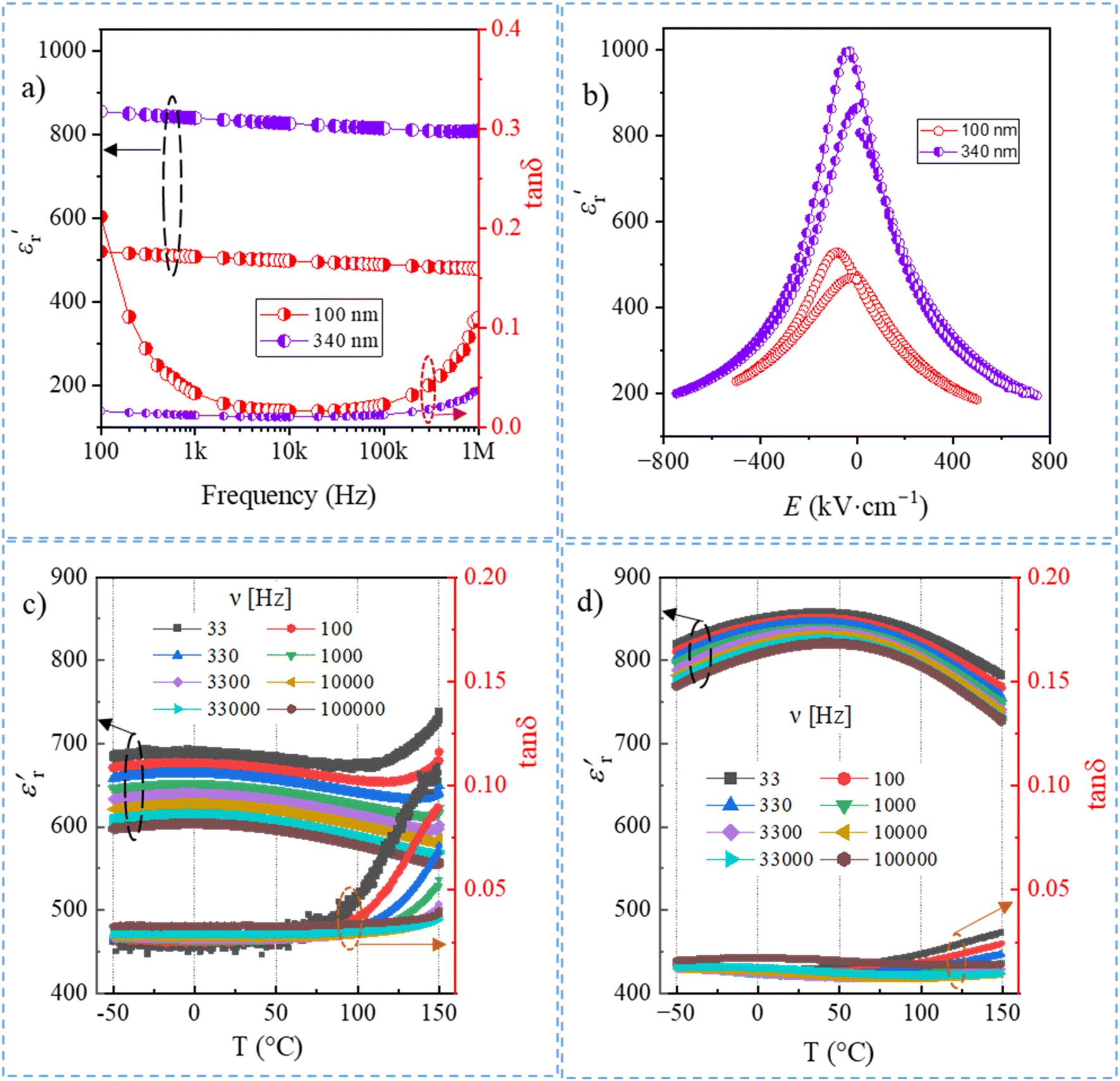 | ||
| Fig. 4 Room-temperature dielectric properties as a function of (a) frequency, and (b) electric field of BZT–BCT-100 and BZT–BCT-340 films. The relative dielectric permittivity and losses of (c) BZT–BCT-100 and (d) BZT–BCT-340 films as functions of temperature at different frequencies (ν). | ||
The double peak of the electric field-dependent relative permittivity of the films indicates their ferroelectric behavior (Fig. 4b).14,27 The imprint nature of  peaks can be due to the different work functions of platinum bottom electrode and gold top electrode.28 In addition, rf-sputtering which was used to deposit electrodes can introduce charged defects that result in asymmetry in the electric field-dependent capacitance measurements.29,30
The frequency-dependent dielectric permittivity curves of the two films as a function of temperature are shown in Fig. 4c and d. In the case of the BZT–BCT-100 film, there is no evident permittivity peak, which we ascribe to its fine grain size and low film thickness.25,26,31 The losses increase with increasing temperature, which is attributed to the increase in the film's conductivity. However, in the BZT–BCT-340 film, a broad permittivity peak is observed between 40 °C and 50 °C, which we attribute to a diffuse phase transition.
In our previous study, about 110 nm thick films with the same composition (1 mole% Mn dopant) but deposited on Pt/Si substrates exhibited a broad dielectric permittivity peak with transition temperature in the range from 55 to 75 °C.14 Compared to the phase transition temperatures of the films on Pt/Si substrates, a further downshift of the permittivity peak of the BZT–BCT-340 on the sapphire substrate is presumably related to the tensile stress developed in the film due to thermal expansion mismatch.15 A weak frequency dispersion could indicate a relaxor-like behaviour of the BZT–BCT-340 film.10 The tanδ of BZT–BCT-340 remains below 0.03 in the whole temperature range, up to 150 °C, while in the thinner film, it noticeably increases above 100 °C.
The polarization as a function of the electric field (P–E) is measured for both films at 1 kHz and is shown in Fig. 5. Ferroelectric properties: remanent polarization (Pr), coercive field (Ec), and maximum polarization (Pmax) of both films are collected in Table 2. The thinner film has a lower Pmax, and rounded tips of the loop indicate leakage contribution. The thicker film has a higher Pmax and sharp tips. The higher coercive field and remanent polarization in the thinner films could be related to the existence of the so-called “dead layers” in addition to the grain size effect and leakage contribution. The dead or nonswitching layers are the interfacial discontinuity at the electrode–ferroelectric material interface, affecting the polarization and coercive field.32–34
 | ||
| Fig. 5 P–E loops of BZT–BCT-100 and BZT–BCT-340 measured at 1 kHz and at room temperature. | ||
| Film | E max (MV cm−1) | E c (kV cm−1) | P r (μC cm−2) | P max (μC cm−2) |
|---|---|---|---|---|
| BZT–BCT-100 | 1 | 110 | 6 | 28 |
| BZT–BCT-340 | 1 | 45 | 4 | 36 |
The BZT–BCT-340 exhibits better dielectric and ferroelectric properties with higher relative dielectric permittivity, lower losses, and significantly higher maximum polarization than the BZT–BCT-100. Due to its slim P–E loop, low remanent polarization, small coercive field, and high saturated polarization, the thicker BZT–BCT film can be considered a viable candidate for energy storage applications.
We measured the P–E loops of the BZT–BCT-340 film at different temperatures from −50 °C to 100 °C, as shown in Fig. 6. The P–E loops do not show any significant change in the shape in the whole temperature range. The temperature-independent P–E loops of the film could suggest that the polarization as a function of the electric field is rather governed by the existence of nano-domains, i.e., polar nano regions in Mn-doped BZT–BCT films, indicating a relaxor-like behavior as reported in NaNbO3 films or BaTi0.75Zr0.25O3 ceramic,35,36 than the ferroelectric polar phase which should disappear above the Tc. The Pr and Ec measurements from −75 °C to 150 °C show the imprint behavior of Pr and Ec, i.e., asymmetry of positive and negative Pr and Ec, presumably due to the different top and bottom electrodes, as shown in the electric field-dependent dielectric permittivity, see Fig. 4b. A progressive decrease of Pr and Ec with the increase in temperature is observed in Fig. 7a and b, yet, these values are not close to zero. It should be noted that at such high temperatures, the conductivity in the films may increase, contributing to the persistence of apparent Ec and Pr. Still, the existence of the polar nano regions in BZT–BCT thin films cannot be excluded.
 | ||
| Fig. 6 P–E loops of BZT–BCT-340 at different temperatures at 1 kHz. | ||
 | ||
| Fig. 7 (a) Remanent polarization (Pr), and (b) coercive field (Ec) of BZT–BCT-340 measured at different temperatures at the applied electric field of 500 kV cm−1. | ||
Unipolar P–E loops of BZT–BCT-340 films were measured at different electric fields to evaluate the energy storage (ES) properties. Fig. 8 shows the unipolar P–E loops measured at progressively higher electric fields up to 3.5 MV cm−1 at 1 kHz and a P–E loop at an E-field of 3.5 MV cm−1 with calculated recoverable energy and losses. The maximum polarization is about 47 μC cm−2. The calculated recoverable energy (Urec) and energy losses (Uloss) are 46.0 J cm−3 and 5.5 J cm−3, respectively. The charging or stored energy (Ust) is 51.5 J cm−3, and energy storage efficiency (η) is 89.2%. The high energy storage performance is due to the high maximum polarization and a high electric field that the film survives without breakdown.
 | ||
| Fig. 8 (a) Unipolar P–E loops (b) P–E and ES properties at Emax of BZT–BCT-340. The measurements were performed at 1 kHz. | ||
Compared to the energy storage properties of BZT–BCT thin films with different cation molar ratios, or dopants, deposited on different substrates or prepared with different deposition techniques, including Pulsed Laser Deposition (PLD), Ion Beam Sputtering (IBSD),37,38 our BZT–BCT-340 film shows promising performance. The comparison of the reported values with BZT–BCT-340 is summarized in Table 3. For example, the lanthanum-doped (Ba0.904Ca0.096)0.9775 + xLa0.015(Zr0.136Ti0.864)O3 (BCZT) film reported by He et al. has a very high efficiency of about 93%, which is attributed to almost no remanent polarization and a maximum applied field of about 3.33 MV cm−1,39 which is about 5% lower than the field applied to our BZT–BCT-340.
| Film | Dopant | Substrate | Thickness (nm) | Method | E max (MV cm−1) | U rec (J cm−3) | η (%) | Ref. |
|---|---|---|---|---|---|---|---|---|
| BCZTa: (Ba0.955Ca0.045)(Zr0.17Ti0.83)O3. BCZTb: (Ba0.904Ca0.096)0.9775 + 0.0075La0.015(Zr0.136Ti0.864)O3, BZT: Ba(Zr0.35Ti0.65)O3. BFO–STO: 0.4(BiFeO3)–0.6(SrTiO3), PCZ: Pb0.88Ca0.12ZrO3, PLZT: Pb0.9La0.1(Zr0.52Ti0.48)O3, PHO: PbHfO3, ITO/glass: indium tin oxide deposited on glass substrate. | ||||||||
| BZT–BCT | — | Pt/Si | 150 | IBSD | 0.15 | 2.3 | 28.5 | 37 |
| BCZTa | — | MgO | 360 | PLD | 2.08 | 39 | 33 | 38 |
| BCZTb | La | Pt/Si | 280 | CSD | 3.335 | 15 | 93 | 39 |
| BZT–BCT | Mn | Pt/Si | 120 | CSD | 1.16 | 10 | 69 | 14 |
| BZT | Sm | STO | 1000 | PLD | 7 | 133 | 89 | 40 |
| BFO–STO | — | STO | 500 | PLD | 3.85 | 70 | 70 | 41 |
| PCZ | — | Pt/Si | 300 | CSD | 2.8 | 50 | 83 | 42 |
| PLZT | La | Ti-foil | 1200 | PLD | 3 | 41 | 80 | 43 |
| PHO | — | ITO/glass | 330 | CSD | 3 | 25 | 73 | 44 |
| BZT–BCT | Mn | Pt/Sa | 340 | CSD | 3.5 | 46 | 89 | This work |
The energy storage efficiency of our BZT–BCT-340 is above or comparable to the values obtained by antiferroelectric and relaxor barium-, lead- and bismuth-based perovskite thin films which are considered to be the ideal candidates for energy storage, for details, please refer to Table 3.
4. Conclusion
We prepared Mn-doped BZT–BCT thin films by chemical solution deposition on platinized sapphire substrates in a multistep deposition and annealing process at 850 °C. The about 100 nm and 340 nm thick crack-free films with columnar microstructure were achieved. The platinized sapphire substrate with a thermal expansion coefficient closer to that of BZT–BCT is a better choice for preparing crack-free BZT–BCT thin films with a thickness of a few 100 nm compared to the commonly used platinized silicon substrate with much lower thermal expansion coefficient resulting in the crack-generation often observed in BT-based thin films with thicknesses above 100 nm. The 100 nm thick BZT–BCT film exhibits a dielectric permittivity of about 500 at 1 kHz, which is 64% lower than the permittivity of the 340 nm thick film. The latter film is characterized by a slim polarization–electric field loop which persists well above the dielectric permittivity peak between 40 °C and 50 °C, suggesting its relaxor-like behavior. The recoverable energy of 46 J cm3 with an energy storage efficiency of about 89% was achieved at 3.5 MV cm−1. The properties of the BZT–BCT thin films reveal their promising potential for energy storage applications in a wide temperature range from −75 °C up to about 150 °C.Data availability
The authors declare that the data supporting the findings of this study are available within the paper.Conflicts of interest
There are no conflicts of interest to declare.Acknowledgements
Slovenian Research and Innovation Agency (core funding P2-0105, J7-4637, P1-0125, S. W. K. – young researcher programme and bilateral cooperations BI-US/22-24-039 and BI-US/24-26-094), MSCA-PF grant agreement no. 101110882. Vid Bobnar is acknowledged for providing access to the impedance analyzer and Aixacct TF Analyzer 2000. Barnik Mandal and Sebastjan Glinšek acknowledge Luxembourg National Research Fund (FNR) for financial support through the project INTER/NWO/20/15079143/TRICOLOR. Geoff Brennecka acknowledges financial support by the Fulbright US Scholar Program, which is sponsored by the US Department of State. Dean Birmančević is acknowledged for his help related to the film deposition.References
- F. MacDougall, T. Jow, J. Ennis, X. Yang, S. Yen, R. Cooper and J. Bates, Pulsed power and power conditioning capacitors, Acta Phys. Pol. A, 2009, 115(6), 989–991, DOI:10.12693/APhysPolA.115.989
.
- X. Li, X. Chen, J. Sun, M. Zhou and H. Zhou, Novel lead-free ceramic capacitors with high energy density and fast discharge performance, Ceram. Int., 2020, 46(3), 3426–3432, DOI:10.1016/j.ceramint.2019.10.055
- M. Peddigari, J. H. Park, J. H. Han, C. K. Jeong, J. Jang, Y. Min and G. T. Hwang, Flexible self-charging, ultrafast, high-power-density ceramic capacitor system, ACS Energy Lett., 2021, 6(4), 1383–1391, DOI:10.1021/acsenergylett.1c00170
- H. Palneedi, M. Peddigari, G. T. Hwang, D. Y. Jeong and J. Ryu, High-performance dielectric ceramic films for energy storage capacitors: progress and outlook, Adv. Funct. Mater., 2018, 28(42), 1803665, DOI:10.1002/adfm.201803665
- A. Ben Amar, A. B. Kouki and H. Cao, Power approaches for implantable medical devices, Sensors, 2015, 15(11), 28889–28914, DOI:10.3390/s151128889
- J. P. Silva, K. C. Sekhar, H. Pan, J. L. MacManus-Driscoll and M. Pereira, Advances in dielectric thin films for energy storage applications, revealing the promise of group IV binary oxides, ACS Energy Lett., 2021, 6(6), 2208–2217, DOI:10.1021/acsenergylett.1c00313
- V. Veerapandiyan, F. Benes, T. Gindel and M. Deluca, Strategies to improve the energy storage properties of perovskite lead-free relaxor ferroelectrics: a review, Materials, 2020, 13(24), 5742, DOI:10.3390/ma13245742
- V. S. Puli, D. K. Pradhan, D. B. Chrisey, M. Tomozawa, G. L. Sharma, J. F. Scott and R. S. Katiyar, Structure, dielectric, ferroelectric, and energy density properties of (1− x) BZT–x BCT ceramic capacitors for energy storage applications, J. Mater. Sci., 2013, 48, 2151–2157, DOI:10.1007/s10853-012-6990-1
- R. Syal, R. Goel, A. De, A. K. Singh, G. Sharma, O. P. Thakur and S. Kumar, Flattening of free energy profile and enhancement of energy storage efficiency near morphotropic phase boundary in lead-free BZT-xBCT, J. Alloys Compd., 2021, 873, 159824, DOI:10.1016/j.jallcom.2021.159824
- S. Lu, G. Chen, Y. Zhang, Z. Zhao, F. Li, Z. Lv and S. Li, Electrocaloric effect in lead-free 0.5Ba(Zr0.2Ti0.8)O3-0.5(Ba0.7Ca0.3)TiO3 ceramic measured by direct and indirect methods, Ceram. Int., 2018, 44(17), 21950–21955, DOI:10.1016/j.ceramint.2018.08.308
- W. L. Li, T. D. Zhang, D. Xu, Y. F. Hou, W. P. Cao and W. D. Fei, LaNiO3 seed layer induced enhancement of piezoelectric properties in (100)-oriented (1−x) BZT–xBCT thin films, J. Eur. Ceram. Soc., 2015, 35(7), 2041–2049, DOI:10.1016/j.jeurceramsoc.2015.01.018
- J. Xu, Y. Zhou, Z. Li, C. Lin, X. Zheng, T. Lin and F. Wang, Microstructural, ferroelectric and photoluminescence properties of Er3+-doped Ba0.85Ca0.15Ti0.9Zr0.1O3 thin films, Mater. Chem. Phys., 2021, 262, 124320, DOI:10.1016/j.matchemphys.2021.124320
- S. W. Konsago, K. Žiberna, B. Kmet, A. Benčan, H. Uršič and B. Malič, Chemical Solution Deposition of Barium Titanate Thin Films with Ethylene Glycol as Solvent for Barium Acetate, Molecules, 2022, 27(12), 3753, DOI:10.3390/molecules27123753
- S. W. Konsago, K. Žiberna, A. Matavž, B. Mandal, S. Glinšek, Y. Fleming, A. Benčan, L. G. Brennecka, H. Uršič and B. Malič, Engineering the Microstructure and Functional Properties of 0.5Ba(Zr0.2Ti0.8)O3-0.5(Ba0.7Ca0.3)TiO3 Thin Films, ACS Appl. Electron. Mater., 2024, 6(6), 4467–4477, DOI:10.1021/acsaelm.4c00530
- T. Pečnik, S. Glinšek, B. Kmet and B. Malič, Combined effects of thickness, grain size and residual stress on the dielectric properties of Ba0.5Sr0.5TiO3 thin films, J. Alloys Compd., 2015, 646, 766–772, DOI:10.1016/j.jallcom.2015.06.192
- L. J. Sinnamon, M. M. Saad, R. M. Bowman and J. M. Gregg, Exploring grain size as a cause for “dead-layer” effects in thin film capacitors, Appl. Phys. Lett., 2002, 81(4), 703–705, DOI:10.1063/1.1494837
- W. J. Lee, H. G. Kim and S. G. Yoon, Microstructure dependence of electrical properties of (Ba0.5Sr0.5)TiO3 thin films deposited on Pt/SiO2/Si, J. Appl. Phys., 1996, 80(10), 5891–5894, DOI:10.1063/1.363583
- G. Kang, K. Yao and J. Wang, (1−x) Ba(Zr0.2Ti0.8)O3–x (Ba0.7Ca0.3)TiO3 Ferroelectric Thin Films Prepared from Chemical Solutions, J. Am. Ceram. Soc., 2012, 95(3), 986–991, DOI:10.1111/j.1551-2916.2011.04877.x
- P. S. Barbato, V. Casuscelli, P. Aprea, R. Scaldaferri and D. Caputo, Optimization of the production process of BZT–BCT sol–gel thin films obtained from a highly stable and green precursor solution, Mater. Manuf. Processes, 2021, 36(14), 1642–1649, DOI:10.1080/10426914.2021.1926495
- S. W. Konsago, A. Debevec, J. Cilenšek, B. Kmet and B. Malič, Linear Thermal Expansion of 0.5 Ba(Zr0.2Ti0.8)O3-0.5(Ba0.7Ca0.3)TiO3 Bulk Ceramic, Inf. MIDEM, 2023, 53(4), 233–238, DOI:10.33180/InfMIDEM2023.403
- W. M. Yim and R. J. Paff, Thermal expansion of AlN, sapphire, and silicon, J. Appl. Phys., 1974, 45(3), 1456–1457, DOI:10.1063/1.1663432
- M. Okaji, Absolute thermal expansion measurements of single-crystal silicon in the range 300–1300 K with an interferometric dilatometer, Int. J. Thermophys., 1988, 9, 1101–1109, DOI:10.1007/BF01133277
- T. Schenk, C. M. Fancher, M. H. Park, C. Richter, C. Künneth, A. Kersch, L. Jacob, J. L. Jones, T. Mikolajick and U. Schroeder, On the origin of the large remanent polarization in La: HfO2, Adv. Electron. Mater., 2019, 5(12), 1900303, DOI:10.1002/aelm.201900303
- K. Maruyama, Y. Kawakami and F. Narita, Young's modulus and ferroelectric property of BaTiO3 films formed by aerosol deposition in consideration of residual stress and film thickness, Jpn. J. Appl. Phys., 2022, 61(SN), SN1011, DOI:10.35848/1347-4065/ac7d96
-
U. Böttger, Dielectric Properties of Polar Oxides, in Polar Oxides, ed. R. Waser, U. Böttger and S. Tiedke, Wiley, 2004, pp. 11–38, DOI:10.1002/3527604650.ch1
- J. F. Ihlefeld, J. P. Maria and W. Borland, Dielectric and microstructural properties of barium titanate zirconate thin films on copper substrates, J. Mater. Res., 2005, 20(10), 2838–2844, DOI:10.1557/JMR.2005.0342
- R. Placeres-Jiménez, J. P. Rino and J. A. Eiras, Modeling ferroelectric permittivity dependence on electric field and estimation of the intrinsic and extrinsic contributions, J. Phys. D: Appl. Phys., 2015, 48(3), 035304, DOI:10.1088/0022-3727/48/3/035304
- L. Pintilie, I. Vrejoiu, D. Hesse and M. Alexe, The influence of the top-contact metal on the ferroelectric properties of epitaxial ferroelectric Pb (Zr0.2Ti0.8)O3 thin films, J. Appl. Phys., 2008, 104(11), 114101, DOI:10.1063/1.3021293
- A. Matavž, J. Kovač, M. Čekada, B. Malič and V. Bobnar, Enhanced electrical response in ferroelectric thin film capacitors with inkjet-printed LaNiO3 electrodes, Appl. Phys. Lett., 2018, 113(1), 012904, DOI:10.1063/1.5037027
- Y. Ahn and J. Y. Son, Imprint phenomenon of ferroelectric switching characteristics in BaTiO3/PbTiO3 multilayer thin films, J. Alloys Compd., 2022, 891, 162088, DOI:10.1016/j.jallcom.2021.162088
- V. Buscaglia, M. T. Buscaglia, M. Viviani, L. Mitoseriu, P. Nanni, V. Trefiletti and J. Petzelt, Grain size and grain boundary-related effects on the properties of nanocrystalline barium titanate ceramics, J. Eur. Ceram. Soc., 2006, 26(14), 2889–2898 CrossRef CAS
- S. K. Streiffer, C. Basceri, C. B. Parker, S. E. Lash and A. I. Kingon, Ferroelectricity in thin films: The dielectric response of fiber-textured (BaxSr1− x)Ti1+y O3+ z thin films grown by chemical vapor deposition, J. Appl. Phys., 1999, 86(8), 4565–4575, DOI:10.1063/1.371404
- L. J. Sinnamon, M. M. Saad, R. M. Bowman and J. M. Gregg, Exploring grain size as a cause for “dead-layer” effects in thin film capacitors, Appl. Phys. Lett., 2002, 81(4), 703–705, DOI:10.1063/1.1494837
- J. Pérez De La Cruz, E. Joanni, P. M. Vilarinho and A. L. Kholkin, Thickness effect on the dielectric, ferroelectric, and piezoelectric properties of ferroelectric lead zirconate titanate thin films, J. Appl. Phys., 2010, 108(11), 114106, DOI:10.1063/1.3514170
- B. Cai, J. Schwarzkopf, E. Hollmann, D. Braun, M. Schmidbauer, T. Grellmann and R. Wördenweber, Electronic characterization of polar nanoregions in relaxor-type ferroelectric NaNbO3 films, Phys. Rev. B, 2016, 93(22), 224107, DOI:10.1103/PhysRevB.93.224107
- T. Badapanda, S. K. Rout, S. Panigrahi and T. P. Sinha, Phase formation and dielectric study of Bi doped BaTi0.75Zr0.25O3 ceramic, Curr. Appl Phys., 2009, 9(4), 727–731, DOI:10.1016/j.cap.2008.06.014
- J. P. Silva, J. M. Silva, M. J. Oliveira, T. Weingärtner, K. C. Sekhar, M. Pereira and M. J. Gomes, High-performance ferroelectric–dielectric multilayered thin films for energy storage capacitors, Adv. Funct. Mater., 2019, 29(6), 1807196, DOI:10.1002/adfm.201807196
- V. S. Puli, D. K. Pradhan, S. Adireddy, R. Martínez, P. Silwal, J. F. Scott and R. S. Katiyar, Nanoscale polarisation switching and leakage currents in (Ba0.955Ca0.045)(Zr0.17Ti0.83)O3 epitaxial thin films, J. Phys. D: Appl. Phys., 2015, 48(35), 355502, DOI:10.1088/0022-3727/48/35/355502
- S. He, B. Peng, G. J. Leighton, C. Shaw, N. Wang, W. Sun and Q. Zhang, High-performance La-doped BCZT thin film capacitors on LaNiO3/Pt composite bottom electrodes with ultra-high efficiency and high thermal stability, Ceram. Int., 2019, 45(9), 11749–11755, DOI:10.1016/j.ceramint.2019.03.051
- H. T. Vu, H. N. Vu, G. Rijnders and M. D. Nguyen, Sm-doping driven state-phase transition and energy storage capability in lead-free Ba (Zr0.35Ti0.65)O3 films, J. Alloys Compd., 2023, 968, 171837, DOI:10.1016/j.jallcom.2023.171837
- H. Pan, J. Ma, J. Ma, Q. Zhang, X. Liu, B. Guan and C. W. Nan, Giant energy density and high efficiency achieved in bismuth ferrite-based film capacitors via domain engineering, Nat. Commun., 2018, 9(1), 1813, DOI:10.1038/s41467-018-04189-6
- Y. Z. Li, Z. J. Wang, Y. Bai and Z. D. Zhang, High energy storage performance in Ca-doped PbZrO3 antiferroelectric films, J. Eur. Ceram. Soc., 2020, 40(4), 1285–1292, DOI:10.1016/j.jeurceramsoc.2019.11.063
- C. T. Nguyen, H. N. Vu and M. D. Nguyen, High-performance energy storage and breakdown strength of low-temperature laser-deposited relaxor PLZT thin films on flexible Ti-foils, J. Alloys Compd., 2019, 802, 422–429, DOI:10.1016/j.jallcom.2019.06.205
- X. X. Huang, T. F. Zhang, W. Wang, P. Z. Ge and X. G. Tang, Tailoring energy-storage performance in antiferroelectric PbHfO3 thin films, Mater. Des., 2021, 204, 109666, DOI:10.1016/j.matdes.2021.109666
| This journal is © The Royal Society of Chemistry 2025 |