
 Open Access Article
 This Open Access Article is licensed under a Creative Commons Attribution-Non Commercial 3.0 Unported Licence
A leveling–shielding dual strategy enabling stable zinc anodes to exhibit ultra-low interfacial impedance
Qing
Wen
abc,
Taixu
Hao
a,
Tian
Chen
abc,
Dinghao
Le
abc,
Pei
Yang
abc,
Hezhang
Chen
 d,
Linbo
Tang
e,
Qing
Wu
f,
Xiahui
Zhang
*abc and
Junchao
Zheng
*abc
d,
Linbo
Tang
e,
Qing
Wu
f,
Xiahui
Zhang
*abc and
Junchao
Zheng
*abc
aSchool of Metallurgy and Environment, Central South University, Changsha 410083, China. E-mail: xhzhang@csu.edu.cn; jczheng@csu.edu.cn
bEngineering Research Center of the Ministry of Education for Advanced Battery Materials, Central South University, Changsha 410083, China
cNational Energy Metal Resources and New Materials Key Laboratory, Central South University, Changsha 410083, China
dSchool of Chemistry and Chemical Engineering, Hunan University of Science and Technology, Xiangtan 411201, China
eSchool of Materials and Environmental Engineering, Changsha University, Changsha, Hunan 410022, China
fSchool of Information and Network Center Central South University, Changsha 410083, China
First published on 13th August 2025
Abstract
Aqueous zinc-ion batteries have demonstrated great potential for large-scale energy storage, but still suffer from severe dendrites and corrosion problems. Uneven distributions of crystalline planes and passivation layers on the zinc anode are the key factors causing dendrites and corrosion. However, the synergistic construction of uniform crystal planes and shielding layers is still challenging. Herein, we propose a novel leveling–shielding dual strategy to stabilize the zinc anode. The low-melting-point indium (In) layer not only serves as a leveling agent to repair surface defects, but also induces uniform and fast deposition of zinc by exposing a single (101)In plane on the anode. Besides, the outer ZnF2 shielding layer can inhibit corrosion and accelerate the de-solvation of Zn(H2O)62+, which improves the electrochemical reaction kinetics. As a result, the ZnF2@In@Zn symmetric cell shows an ultra-low interfacial impedance of <10 Ω and a stable cycle life of >2800 h with a low polarization voltage of 21.8 mV at 5 mA cm−2 and 2 mAh cm−2, compared with bare Zn (140 h and 75.8 mV). Besides, the ZnF2@In@Zn//NH4V4O10 full cell maintains a high capacity of 112.4 mAh g−1 with a retention rate of 79.5% after 10![[thin space (1/6-em)]](https://www.rsc.org/images/entities/char_2009.gif) 000 cycles at 3 A g−1. This work provides a novel, effective leveling–shielding dual strategy for interfacial modification of zinc anodes, which can also be applied in other metal anodes.
000 cycles at 3 A g−1. This work provides a novel, effective leveling–shielding dual strategy for interfacial modification of zinc anodes, which can also be applied in other metal anodes.
1 Introduction
During the critical stage of global energy structure transformation, energy security has become a core issue for the sustainable development of human civilization.1,2 Currently, fossil fuels still dominate the global primary energy consumption structure (accounting for 79.6%), and 73.2% of the greenhouse gas emissions stem from energy activities.3 While clean energy technologies like photovoltaics and wind power can reduce carbon emission intensity by over 90%, their inherent geographical unevenness and intermittent nature necessitate supporting energy storage systems for stable power output.4–6 Among existing energy storage technologies, lithium-ion batteries are subject to high costs and thermal runaway risks, which hinder their ability to meet large-scale storage needs;7 pumped storage, though economical, demands strict geographical conditions (requiring elevation drops exceeding 400 m).8 Thanks to high volumetric energy density (5850 mAh cm−3), cost-effectiveness, and inherent non-flammability, aqueous zinc ion batteries have emerged as promising candidates for large-scale energy storage.9–12 However, uncontrolled dendrite growth and interfacial side reactions of the zinc anode during cycling degrade battery cycle stability, thereby restricting industrial application.13–15The uneven distribution of crystal planes and passivation layers (such as Zn2(OH)2CO3 and ZnO) on the zinc anode is a key factor leading to zinc dendrites and corrosion. Various crystal planes, including (002)Zn, (100)Zn and (101)Zn, are randomly distributed on the initial zinc anode. Due to differences in the adsorption energy of zinc on different crystal planes, the zinc anode exhibits uneven zinc deposition dynamics across various regions.16 Meanwhile, the corrosion potentials of different crystal planes vary, leading to the uneven distribution of corrosion and passivation layers.17,18 These differences in deposition dynamics and the uneven distribution of corrosion and passivation layers synergistically accelerate dendrite growth. Additionally, owing to the low overpotential of zinc (−0.76 V vs. the Hydrogen Evolution Reaction (HER)), prolonged corrosion is thermodynamically inevitable in weakly acidic electrolyte (Fig. 1a). Among numerous modification strategies, such as using electrolyte additives,19,20 high-concentration electrolytes,21,22 and hydrogel electrolytes,23,24 significant progress has been achieved in mitigating dendrite formation and corrosion. However, these approaches have exhibited limited efficacy in addressing the uneven distributions of crystal planes and passivation layers on the anode. Interfacial modification, which can improve the surface properties of the anode, has garnered substantial research attention and is considered a promising strategy to solve these challenges.25,26
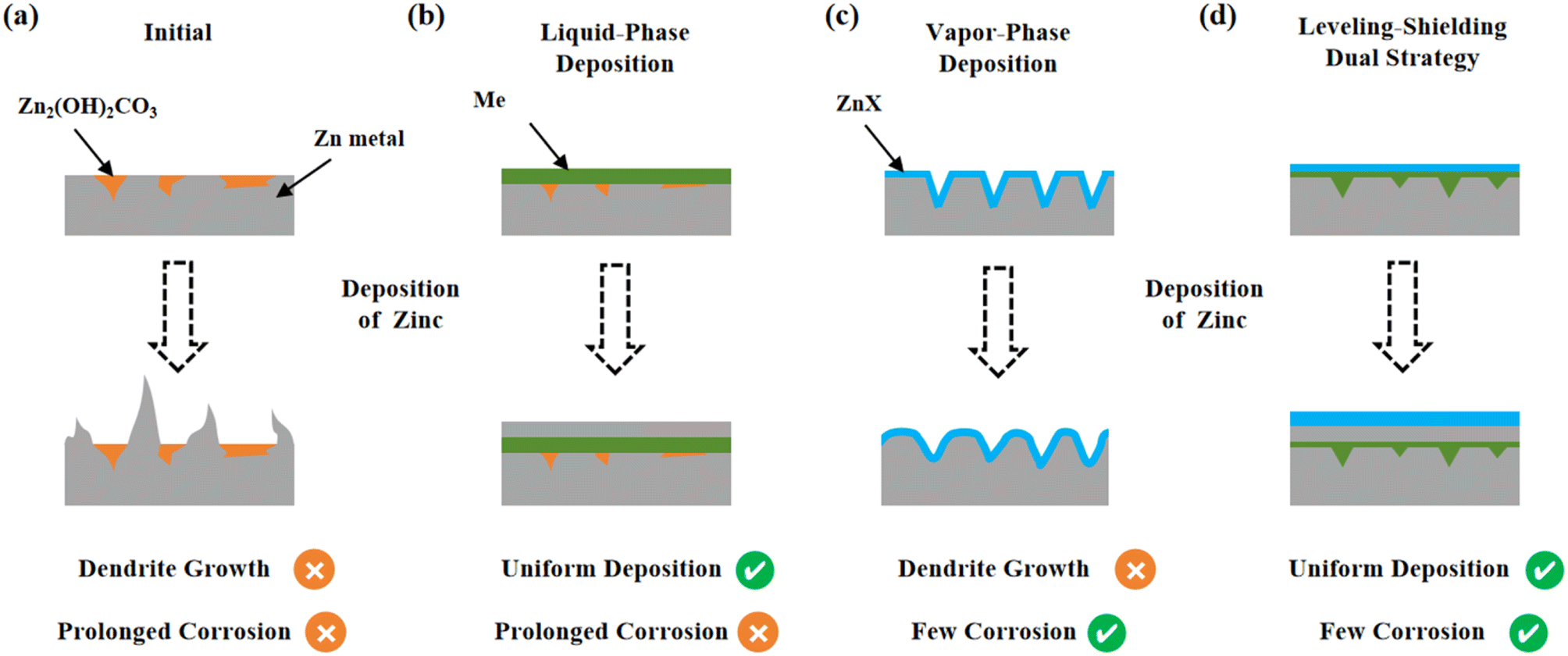 | ||
| Fig. 1 Schematic illustration of dendrite growth and corrosion at the modified interface. (a) Bare Zn, (b) metal modified layer by liquid-phase deposition, (c) metal compound modified layer by vapor-phase deposition and (d) metal and metal compound composite layer by a leveling–shielding dual strategy. | ||
Commonly used interface modification methods can be categorized into physical coating, liquid-phase deposition, and vapor-phase deposition. Physical coating relies on adhesive bonding with the anode, which struggles to achieve molecular-level coverage and offers limited enhancement to the properties of initial zinc.26 In contrast, liquid-phase and vapor-phase deposition are in situ growth methods requiring chemical reactions with zinc metal, which can improve the surface properties of initial zinc. For instance, some high-potential metals (such as In,27 Cu28 and Sn29) can replace zinc through liquid-phase deposition to form a metal modification layer on the zinc anode. The specific crystal planes of these metals facilitate uniform zinc deposition (Fig. 1b). However, the corrosion issue of deposited zinc remains unsolved. Depositing metal compounds (such as ZnF2,30–32 ZnSe33 and ZnS33) with high ionic conductivity on the anode through vapor-phase deposition can hinder the contact between the deposited zinc and the electrolyte, thereby inhibiting the prolonged corrosion of zinc (Fig. 1c). However, the decomposition of Zn2(OH)2CO3 results in holes on the anode during vapor-phase deposition, which is detrimental to uniform deposition. Additionally, the uneven distribution of zinc crystal planes within the coating layer still poses the risk of dendrite growth. Therefore, it is urgent to develop a modified layer with uniformly distributed crystal planes and passivation layers to simultaneously inhibit dendrites and corrosion.
Herein, we propose a leveling–shielding dual strategy to construct a stable Zn anode (Fig. 1d). The low-melting-point In metal serves as a leveling agent to repair surface defects caused by the decomposition of Zn2(OH)2CO3 during heat treatment. The exposed single (101)In plane can induce uniform and rapid deposition of zinc. The outermost ZnF2 shielding layer can inhibit the corrosion of deposited zinc and accelerate the de-solvation process of Zn(H2O)62+, which further improves the electrochemical reaction kinetics. As a result, the ZnF2@In@Zn symmetric cell demonstrates an ultra-low interfacial impedance of less than 10 Ω and achieves stable cycling for over 2800 h with a polarization voltage of 21.8 mV at 5 mA cm−2 and 2 mAh cm−2, a significant improvement over that of bare Zn (140 h, 75.8 mV). Additionally, the ZnF2@In@Zn//NH4V4O10 full cell retains a capacity of 112.4 mAh g−1 after 10000 cycles at 3 A g−1, corresponding to a capacity retention rate of 79.5%.
2 Results and discussion
The leveling–shielding dual strategy involves two stages of in situ deposition: the In metal layer is constructed through liquid-phase deposition and the ZnF2 layer is constructed by vapor-phase deposition (Fig. 2a). Based on the Zn–In binary metal phase diagram (Fig. S1), during vapor-phase deposition, the In metal and surface Zn metal undergo eutectic melting to form a homogeneous melt. Given that Zn has a lower potential than In, HF produced by the decomposition of NH4F selectively reacts with Zn to produce ZnF2, which deposits on the surface. As cooling begins, Zn preferentially precipitates from the melt with the formation of grain boundaries. With further cooling, the ZnIn alloy can infiltrate into the grain boundaries and holes, precipitating within them and effectively healing surface defects. The reactions involved in this entire process are as follows:| 3Zn (s) + 2InCl3 (aq) → 3ZnCl2 (aq) + 2In (s) | (1) |
 | (2) |
 | (3) |
 | ||
| Fig. 2 Surface morphology analysis of various anodes. (a) Schematic diagram of the preparation of a ZnF2@In@Zn anode by the leveling–shielding dual strategy. SEM images of (b) bare Zn, (c) In@Zn, (d) ZnF2@Zn and (e) ZnF2@In@Zn. (f) Mapping images of ZnF2@In@Zn. Metallographic microscope image of (g) bare Zn, (h) In@Zn, (i) ZnF2@Zn and (j) ZnF2@In@Zn. | ||
Scanning electron microscopy (SEM) reveals the morphological evolution during the construction of the ZnF2@In@Zn anode. The initial zinc surface is smooth and flat (Fig. 2b and S2a). After liquid-phase deposition, the surface morphology of the In@Zn anode remains largely unchanged, possibly due to the strong binding energy between In and Zn, which allows In to be embedded within the Zn lattice to form a ZnIn alloy (Fig. 2c and S2b). In the absence of In, tiny holes emerge on the surface of ZnF2@Zn (Fig. 2d and S2c). In contrast, the ZnF2@In@Zn anode maintains a relatively flat surface (Fig. 2e and S2d). Compared to ZnF2@Zn, the heat-treated Zn exhibits larger and denser holes in the Ar atmospheres (Fig. S2e and f). This indicates that the holes are formed by the decomposition of Zn2(OH)2CO3 on the zinc surface. Notably, the ZnF2 produced by vapor-phase deposition can partially fill these holes. The mapping diagram illustrates the distribution of elements. The surface of bare Zn is covered with C, O, and Zn elements, and EDS also detected a certain amount of C and O elements, indicating the presence of Zn2(OH)2CO3 on the bare Zn surface (Fig. S3). In both the In@Zn and ZnF2@Zn anodes, elements are uniformly distributed, indicating an even modification layer on the zinc surface (Fig. S4). For the ZnF2@In@Zn anode, F and Zn elements are also evenly distributed, showing that the ZnF2 layer is uniformly constructed (Fig. 2f). However, In distribution on the ZnF2@In@Zn surface is localized in spots and lines (Fig. 2f). This suggests that during cooling, In metal fills the grain boundaries and pores of zinc, repairing surface defects. Besides, the ZnF2@In@Zn anode exhibits a distinct trilayer structure. Layer A is a ZnF2 layer, layer B mainly consists of In, and layer C is primarily composed of Zn. The thickness of the ZnF2 layer is approximately 6.8 μm and the thickness of the In layer is about 1 μm (Fig. S5). As shown in the In element distribution mapping, In metal tends to concentrate in the depressions. This further confirms that In metal fills the grain boundaries and pores of zinc. The metallographic microscope image reveals the occurrence form of metals on the surface. The inert passivation layer appears black due to its low reflectivity, whereas metals with high reflectivity exhibit a bright golden color. On the bare Zn surface, bright golden and black spots are randomly distributed, indicating an uneven passivation layer (Fig. 2g). For the In@Zn anode, the black spots are reduced, yet the color distribution remains non-uniform, suggesting that some passivation layer exists (Fig. 2h). Thanks to the uniform distribution of ZnF2, the ZnF2@Zn and ZnF2@In@Zn anodes show a uniform orange-yellow color (Fig. 2i and j).
X-ray diffraction (XRD) and X-ray photoelectron spectroscopy (XPS) reveal the surface material composition. The XRD pattern of bare Zn corresponds well with the standard spectrum (PDF #01-1238) (Fig. 3a). A weak peak attributable to ZnF2, in accordance with PDF #07-0214, is present in the diffraction profile of the ZnF2@Zn anode (Fig. 3b). For the In@Zn anode, an intense indium peak at 33°, linked to the (101) plane and consistent with PDF #05-0642, is observed. This indicates substantial exposure of the (101)In plane on the anode surface (Fig. 3c). Compared with the ZnF2@Zn anode, the ZnF2@In@Zn anode exhibits a more pronounced ZnF2 peak, suggesting that the melt facilitates the fluorination reaction (Fig. 3c). Additionally, the ZnF2@In@Zn anode shows a reduced In peak intensity, with only the (101)In plane detectable, which could be attributed to the ZnF2 layer partially shielding the In signal (Fig. 3c). It is worth noting that the ZnF2@In@Zn anode displays a higher I(101)Zn/(I(002)Zn + I(100)Zn) peak intensity ratio (∼6.87) compared to bare Zn (∼3.99) (Fig. S6a). Conversely, the In@Zn and ZnF2@Zn anodes exhibit lower ratios than bare Zn (Fig. S6b). This implies that the replacement and fluorination processes do not enhance the exposure of the (101)Zn plane. The increased exposure of the (101)Zn plane on the ZnF2@In@Zn anode may result from the recrystallization of the Zn–In melt along the (101) plane. The full XPS spectrum detects Zn, F, and In peaks on the ZnF2@In@Zn anode (Fig. S7). The Cl peak is found at the In@Zn anode, attributed to residual Cl from the InCl3 solution (Fig. S7). In the high-resolution F 1s XPS spectrum, the F peak in ZnF2@In@Zn is right-shifted relative to ZnF2@Zn (Fig. 3d), likely due to the binding of some of the In and F. The high-resolution In 3d XPS spectrum shows that the In peak in ZnF2@In@Zn is left-shifted compared to In@Zn (Fig. 3e), further indicating the binding of In and F. In the high-resolution Zn 2p XPS spectrum, ZnF2@In@Zn and ZnF2@Zn show left-shifted peaks compared to bare Zn and In@Zn (Fig. 3f), which is because the binding energy between Zn and F is stronger than that between Zn and O.
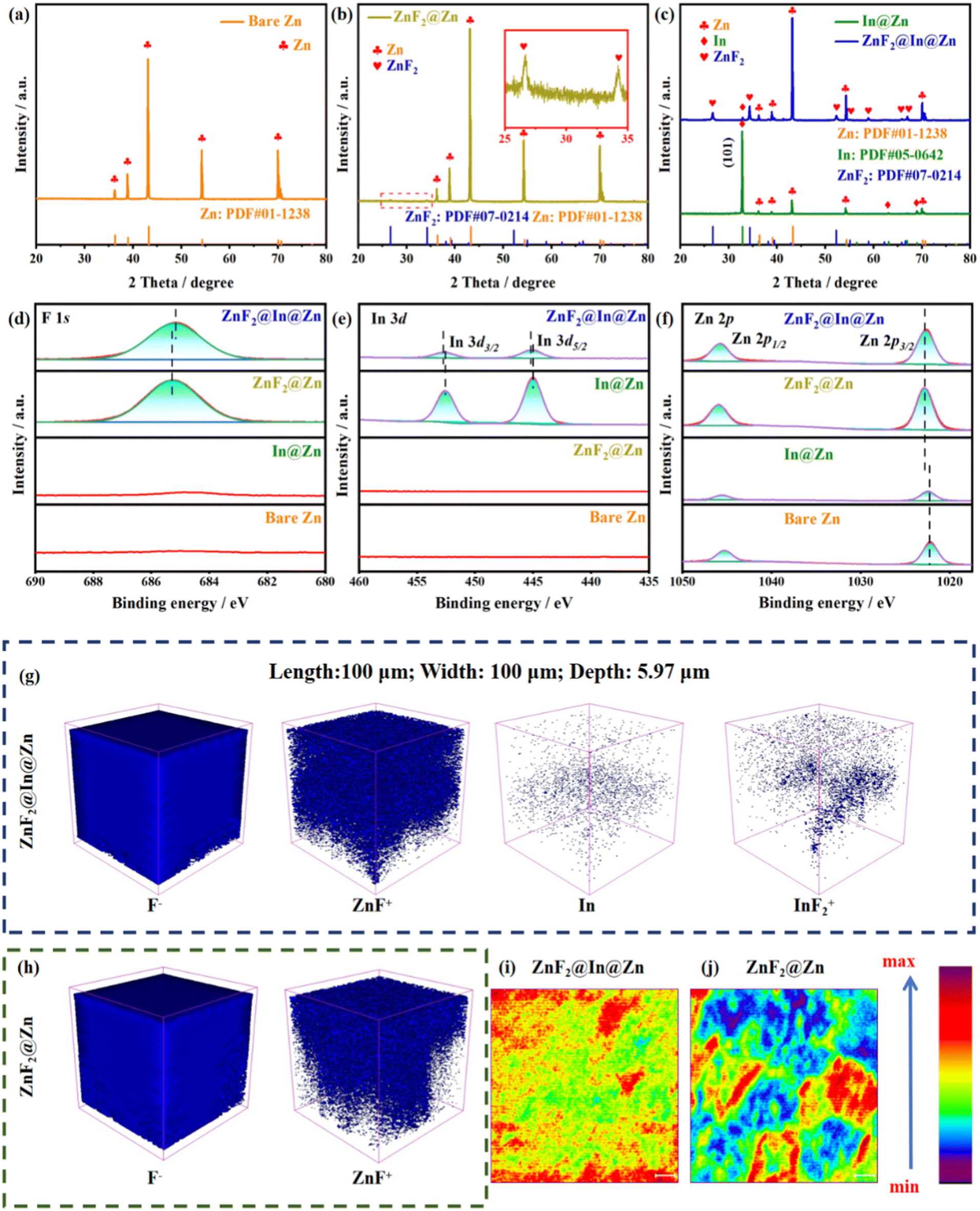 | ||
| Fig. 3 Study of element distribution on various anode surfaces. XRD spectra of (a) bare Zn, (b) ZnF2@Zn, (c) In@Zn and ZnF2@In@Zn. High-resolution (d) F 1s, (e) In 3d and (f) Zn 2p XPS spectra. TOF-SIMS images of (g) ZnF2@In@Zn and (h) ZnF2@Zn. ZnF+ signal intensity of (i) ZnF2@In@Zn and (j) ZnF2@Zn (length: 100 μm; width: 100 μm; depth: 5.97 μm). | ||
Time-of-flight secondary ion mass spectrometry (TOF-SIMS) offers a more intuitive analysis of the elemental distribution on the surfaces of the ZnF2@Zn and ZnF2@In@Zn anodes. Both anode surfaces are densely covered with F− and ZnF+ signals, indicating complete coverage of the outermost layer by ZnF2 (Fig. 3g and h). In the ZnF2@In@Zn anode, the weak In signal suggests that the In layer is enveloped by the ZnF2 layer, which can suppress the corrosion of deposited zinc. Furthermore, the detection of InF2+ signals in the ZnF2@In@Zn anode provides additional evidence of In–F bonding (Fig. 3g). The intensity of the ZnF+ signal on the ZnF2@In@Zn anode is stronger and more uniform than that on the ZnF2@Zn anode (Fig. 3i and j). This may be because the melt accelerates the fluorination reaction, enhancing its completeness, and exhibits good wettability, allowing it to spread evenly across the anode surface.
Benefiting from its surface defect repair and the abundant coverage of ZnF2, the ZnF2@In@Zn anode demonstrates ultrafast electrochemical kinetics, achieving polarization voltages of 7.2, 10.9, 14.6, 21.8, and 38 mV at current densities of 1, 2, 3, 5, and 10 mA cm−2, respectively (Fig. 4a, c and S8). Similarly, ZnF2@Zn (22.4, 25.9, 29.7, 38.8, and 59.8 mV) and In@Zn anodes (12.5, 18.9, 23.9, 34.4, and 58.2 mV) exhibit comparatively low polarization voltages at the same current densities (Fig. 4b, c and S8). In contrast, bare Zn shows significantly highest polarization voltages of 41.6, 53, 62, 75.8, and 96.9 mV at these current densities (Fig. 4a, c and S8). This difference is attributed to interfacial corrosion and dendrite issues in bare Zn. Moreover, ZnF2@In@Zn has a much lower nucleation overpotential of 4.2 mV compared to bare Zn (108.6 mV), In@Zn (36.5 mV), and ZnF2@Zn (32.4 mV) (Fig. 4d, e and S9). This indicates a faster zinc nucleation process and a higher zinc nucleation density for the ZnF2@In@Zn anode. Moreover, compared with bare Zn, the ZnF2@In@Zn anode exhibits superior wettability with electrolytes, which is beneficial for reducing polarization voltage and nucleation overpotential (Fig. S10). To more accurately evaluate the deposition kinetics, we calculated the exchange current density during zinc deposition. As shown in Fig. S11a, bare Zn has a low exchange current density of only 8.7 mA cm−2, whereas ZnF2@In@Zn has a significantly higher value of 14.6 mA cm−2, indicating faster deposition kinetics. Additionally, In@Zn and ZnF2@Zn also exhibit increased exchange current densities compared to bare Zn, demonstrating that both the In layer and the ZnF2 layer can enhance the deposition kinetics (Fig. S11b).
 | ||
| Fig. 4 Study of kinetic processes in symmetric cells. Multiplication performance of symmetric cells assembled with (a) bare Zn, ZnF2@In@Zn, (b) In@Zn and ZnF2@Zn anodes. (c) Polarization voltage histograms of various anodes at different current densities. Voltage–time plots of symmetric cells assembled with (d) bare Zn and (e) ZnF2@In@Zn. EIS of symmetric cells assembled from (f) bare Zn and (g) ZnF2@In@Zn anode at various resting times. (h) Comparison of this work with published studies in terms of current density, polarization voltage and charge transfer impedance.34–40 | ||
To evaluate the corrosion resistance of ZnF2@In@Zn, electrochemical impedance spectroscopy (EIS) is conducted at various resting times. Fig. S12 presents the equivalent circuit diagram, and Table S1 lists the values of solution resistance (Rs), solid electrolyte interfacial impedance (REIS), and charge transfer impedance (Rct) for various anodes at different resting times. As the resting time increased, bare Zn exhibited a continuous rise in both REIS and Rct, indicative of ongoing corrosion (Fig. 4f). During the resting period, In@Zn showed fluctuations in REIS and Rct, likely due to temperature variations in the testing environment (Fig. S13a). However, overall, the In@Zn anode maintained extremely low REIS and Rct, highlighting superior corrosion resistance and electronic transport properties of In. The ZnF2@Zn anode experienced a gradual increase in REIS and Rct, possibly due to electrolyte penetration through surface pores (Fig. S13b). Nonetheless, its impedance remained significantly lower than that of bare Zn. Benefiting from In's role in repairing interfacial defects, ZnF2@In@Zn demonstrated the lowest and most stable REIS and Rct of less than 10 Ω (Fig. 4g). This underscores its rapid electrochemical kinetics and excellent corrosion resistance. It is also worth noting that REIS and Rct of In@Zn are marginally higher than those of ZnF2@In@Zn. This slight discrepancy may stem from partial oxidation of In metal during storage and construction. Furthermore, the ZnF2@In@Zn anode similarly demonstrates low polarization voltage and low charge transfer impedance at high current densities compared to other studies on anode modification (Fig. 4h). To further assess the ability of the ZnF2@In@Zn anode to suppress interfacial side reactions, linear sweep voltammetry (LSV) curves of bare Zn and ZnF2@In@Zn anode were measured. Compared with bare Zn (−1.83 V), the ZnF2@In@Zn anode has a lower hydrogen evolution overpotential of −2.01 V (vs. Ag/AgCl) (Fig. S14). This indicates that the ZnF2@In layer effectively suppresses the hydrogen evolution reaction.
The cycle life of ZnF2@In@Zn symmetric cells was further evaluated. Under 1 mA cm−2/1 mAh cm−2 conditions, the ZnF2@In@Zn anode demonstrates stable cycling for over 4000 h, a significant improvement over bare Zn, which fails after only 350 h (Fig. S15). When the current density and deposition amount are increased to 5 mA cm−2/2 mAh cm−2, the ZnF2@In@Zn anode maintains a cycle life exceeding 2800 h, whereas bare Zn survives only for 140 h (Fig. 5a). Under more demanding conditions of 10 mA cm−2/5 mAh cm−2, the ZnF2@In@Zn anode achieves a cycle life of over 500 h with a low polarization voltage of 37 mV, whereas bare Zn fails after 41 h with a polarization voltage of 79 mV (Fig. 5b). Additionally, under 10 mA cm−2/5 mAh cm−2 conditions, ZnF2@Zn and In@Zn anodes also show extended cycle lives of 344 and 100 h (Fig. S16), respectively, compared to bare Zn. This shows that a single protective layer can also improve the cycle stability of the anode. Moreover, the ZnF2@In@Zn anode demonstrates superior cycling stability at various rates compared to other reported studies (Fig. 5c).
 | ||
| Fig. 5 Study of cycling stability in symmetric cells. Cycling performance test of bare Zn and ZnF2@In@Zn symmetric cells at (a) 5 mA cm−2/2 mAh cm−2 and (b) 10 mA cm−2/5 mAh cm−2. (c) Comparison of this work with published work on cycle stability of symmetric cells.34,41–46 (d) EIS of the ZnF2@In@Zn symmetric cell at different temperatures. (e) Arrhenius curve and activation energy of bare Zn and ZnF2@In@Zn anodes based on Rct. (f) Binding models and energies for Zn2+ binding to H2O and ZnF2. (g) Adsorption models and energies of zinc atoms with (100)Zn, (002)Zn and (101)In planes. | ||
Lower polarisation voltage is closely related to deposition kinetics. In general, zinc deposition can be divided into four processes: (1) diffusion of Zn(H2O)62+ to the anode surface; (2) de-solvation of Zn(H2O)62+; (3) transport of Zn2+ from the passivation layer to the surface of the metal layer; (4) the electrical crystallisation. The diffusion of Zn(H2O)62+ to the anode surface is usually consistent as the electrolyte composition remains unchanged. To investigate the effect of bare Zn and ZnF2@In@Zn on the de-solvation of Zn(H2O)62+, the EIS of the symmetric cell was obtained at different temperatures. As the temperature increases, the Rct and RSEI of the bare Zn symmetric battery drop sharply (Fig. S18a), whereas those of the ZnF2@In@Zn symmetric battery decrease only slightly (Fig. 5d). The activation energies for the two impedances of the ZnF2@In@Zn anode, calculated via the Arrhenius equation based on Rct and RSEI at different temperatures, are lower than those of the bare Zn, indicating faster de-solvation of Zn(H2O)62+ (Fig. 5e and S18b). Additionally, ZnF2 exhibits a higher binding energy for Zn2+ (−21.8 eV) compared to H2O (−4.8 eV), indicating its ability to accelerate the de-solvation of Zn(H2O)62+ (Fig. 5f). To evaluate Zn2+ transport in the passivation layer, the ionic transference numbers of the bare Zn and ZnF2@In@Zn anodes were tested and calculated. Compared to bare Zn (0.16), the ZnF2@In@Zn anode has a higher Zn2+ transference number (0.72), showing faster Zn2+ transport through the ZnF2 layer (Fig. S19). Moreover, the (101)In plane has a higher adsorption energy for zinc atoms (−0.42 eV) than the (002)Zn (−0.13 eV) and (100)Zn (−0.23 eV) planes, indicating that the In layer can speed up electrocrystallization of zinc (Fig. 5g). In summary, the faster de-solvation of Zn(H2O)62+, Zn2+ transport, and electrocrystallization processes give the ZnF2@In@Zn anode quicker deposition kinetics than bare Zn, resulting in lower nucleation potential and polarization voltage.
High cycle stability is closely related to uniformity of zinc deposition. When a fixed voltage is applied, a sustained increase in current density over time signifies 2D diffusion, which is prone to dendrite formation. In contrast, the stabilization of current density after an initial increase indicates 3D diffusion, suggesting uniform zinc deposition. The ZnF2@In@Zn and ZnF2@Zn anodes transition to 3D diffusion shortly after the initial 2D diffusion (∼2 s), indicating uniform zinc deposition (Fig. S20). Conversely, the In@Zn anode and bare Zn show continuous 2D diffusion, implying dendrite formation (Fig. S20).
Fig. S21 presents the cyclic voltammetry (CV) curves for bare Zn and ZnF2@In@Zn symmetric cells. Compared to bare Zn, the ZnF2@In@Zn symmetric cell achieves a higher current density as voltage increases, indicative of faster electrochemical kinetics. The voltage sweep from 0 V to 0.15 V is labeled as step 1, and the reverse sweep from 0.15 V to 0 V is step 2. For the bare Zn symmetric cell, the step 2 current density (i2) is more than the step 1 current density (i1) (Fig. S21a). According to the polarization overpotential eqn (4), when the voltage is constant, the limiting current density (ilim2) should be more than the ilim1. According to the relationship between the ilim and the diffusion distance (δ) formula (5), the δ2 is shorter than δ1, indicating the formation of dendrites on the bare Zn surface. In contrast, for the ZnF2@In@Zn symmetric cell, the current densities in steps 1 and 2 are nearly identical, suggesting uniform zinc deposition (Fig. S21b). Moreover, the crystal surface specific energy will affect the current density. In the ZnF2@In@Zn symmetric cell, the current densities in steps 1 and 2 are nearly identical, which also reflects the stable surface energy, which is conducive to uniform deposition.
 | (4) |
 | (5) |
The (101)Zn plane is known for its lower lattice distortion rate and smaller distortion surface energy change.47,48 Under the condition of 1 mA cm−2/1 mAh cm−2, after 25 cycles, ZnF2@In@Zn shows a higher specific intensity (∼9.60) of (101) relative to the sum of (002) and (100) (Fig. S22), compared to (6.87) before cycling (Fig. S6a). This indicates that zinc grows along the (101) plane and increases its exposure. Conversely, bare Zn exhibits a reduced specific intensity (∼2.25) (Fig. S22), which can lead to lattice distortion and uneven surface energy distribution, resulting in dendrite growth.
Confocal laser scanning microscopy (CLSM) was used to analyze the surface roughness (Sa) of the anode. Under 1 mA cm−2/1 mAh cm−2 conditions after 25 cycles, the ZnF2@In@Zn anode shows lower surface roughness (Sa = 1.71) than bare Zn (Sa = 3.09), indicating more uniform deposition (Fig. 6a and b). Additionally, the height profile of ZnF2@In@Zn exhibits smaller fluctuations than bare Zn, further confirming its uniform deposition (Fig. S23). SEM reveals the morphological evolution at varying deposition amounts. For bare Zn with a deposition of 0.5 mAh cm−2, the surface shows small particle accumulation (Fig. 6c). As the deposition increased to 5 mAh cm−2, particle accumulation became more pronounced, with some areas showing no zinc deposition (Fig. 6d). In contrast, the ZnF2@In@Zn anode with a deposition of 0.5 mAh cm−2 displays a uniform distribution of hexagonal zinc particles (Fig. 6e). When the deposition increased to 5 mAh cm−2, these particles merge into a more uniform surface, indicating that they coalesced during deposition (Fig. 6f). Moreover, mapping and the EDS results of the ZnF2@In@Zn anode with a deposition amount of 5 mAh cm−2 show that F remains evenly distributed, whereas In is almost undetectable (Fig. S24). This suggests that zinc deposition occurred between the In layer and the ZnF2 layer, inhibiting corrosion of the deposited zinc. Optical microscopy further revealed the morphological evolution of zinc during deposition. For bare Zn, as deposition progressed, noticeable surface protrusions formed, along with bubble formation (Fig. S25a), which indicates dendrite growth and corrosion. Conversely, the ZnF2@In@Zn anode shows relatively uniform surface deposition with no bubble formation (Fig. S25b).
 | ||
| Fig. 6 Study of anode deposition behavior. CLSM images of (a) bare Zn and (b) ZnF2@In@Zn anodes after 25 cycles at 1 mA cm−2/1 mAh cm−2. SEM images of (c and d) bare Zn and (e and f) ZnF2@In@Zn anodes deposited with (c and e) 0.5 mAh cm−2 and (d and f) 5 mAh cm−2 after 25 cycles at 1 mA cm−2/1 mAh cm−2. Current density profiles of (g) bare Zn and (h) ZnF2@In@Zn anode surfaces in different deposition states. | ||
COMSOL Multiphysics was used to analyze the distributions of current density and Zn2+ concentration on the anode surface during deposition. For the bare Zn, uneven passivation layers cause localized deposition. Areas with localized deposition show high current density, whereas the passivation zones (orange) have low current density, worsening zinc deposition unevenness (Fig. 6g). As deposition becomes more uneven, so does the current density distribution. Throughout the deposition process of bare Zn, Zn2+ tend to gather at surface protrusions with larger specific surface areas (Fig. S26a). For the ZnF2@In@Zn anode, the current density stays uniform during deposition (Fig. 6h). In the field of Zn2+ concentration, the ZnF2 layer (yellow) ensures uniform Zn2+ distribution, promoting uniform zinc deposition on the In layer (olive green) (Fig. S26b).
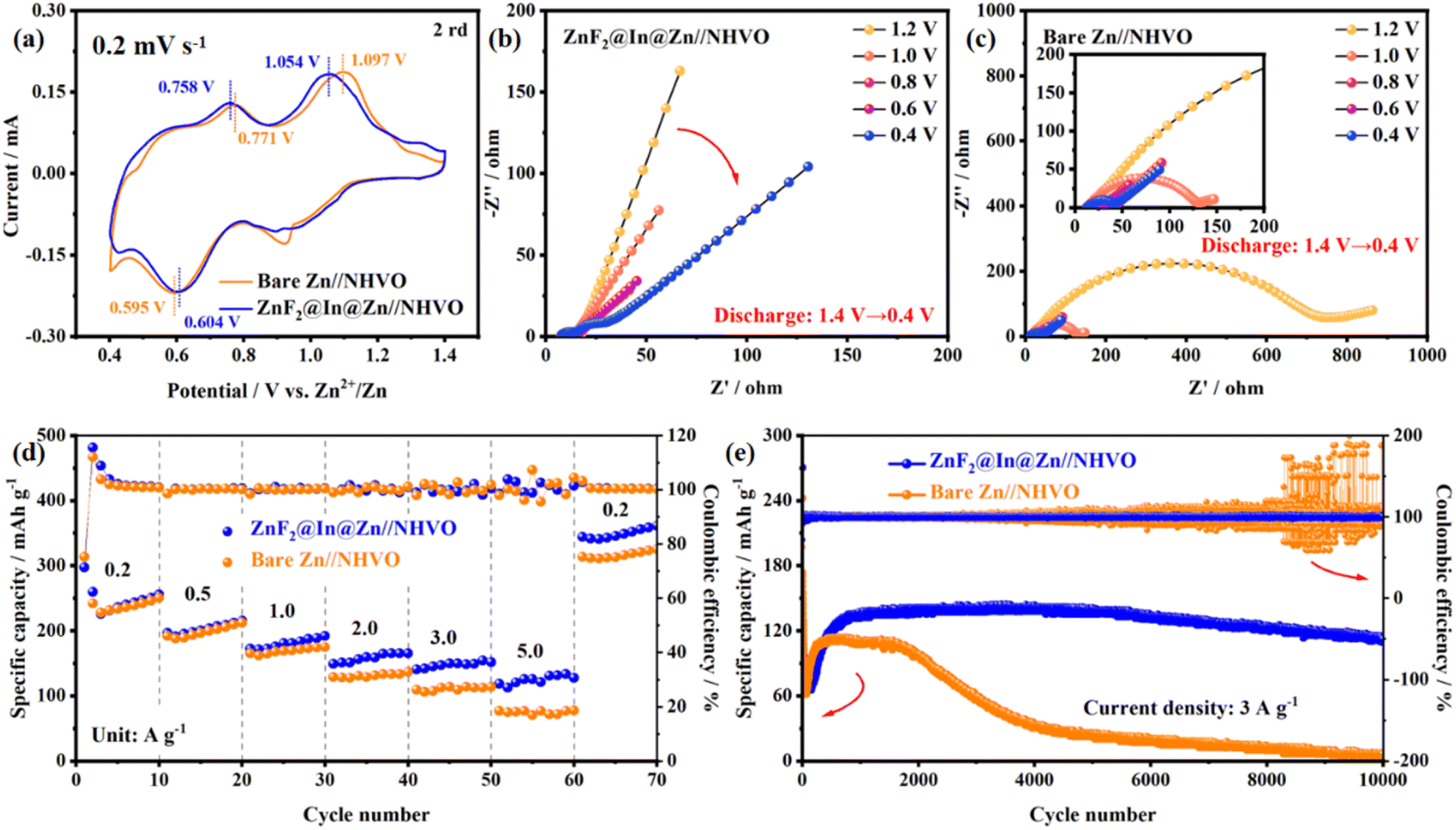
To evaluate the impact of the ZnF2@In@Zn anode on the charge/discharge performance of the cathode, a full cell with NH4V4O10 as the cathode (NHVO) is assembled. Given that the NHVO cathode undergoes structural changes during the first cycle, the second cycle of the cyclic voltammetry (CV) curve is analyzed. The ZnF2@In@Zn//NHVO full cell exhibits lower oxidation peak potentials (1.054 V and 0.758 V) compared to the bare Zn//NHVO full cell (1.097 V and 0.771 V), attributed to its smaller polarization voltage (Fig. 7a). Meanwhile, the reduction peak potential of the ZnF2@In@Zn//NHVO full cell increases from 0.595 V (bare Zn//NHVO full cells) to 0.604 V, indicating improved full cell energy efficiency (Fig. 7a).
 | ||
| Fig. 7 Study of the Zn//NHVO full cell performance. (a) CV curve of bare Zn//NHVO and ZnF2@In@Zn//NHVO full cells. In situ EIS spectra of (b) bare Zn//NHVO and (c) ZnF2@In@Zn//NHVO full cells discharged from 1.4 V to 0.4 V. (d) Rate and (e) cycle performance of the Zn//NHVO full cell. | ||
Fig. S27 presents the equivalent circuit diagram of the Zn//NHVO full cell, and Table S2 lists the values of solution resistance (Rs), solid electrolyte interfacial impedance (REIS), and charge transfer impedance (Rct) for various anodes at different resting times. Electrochemical impedance measurements of the ZnF2@In@Zn//NHVO full cell at various voltages reveal that the Rct of the ZnF2@In@Zn anode remains stable throughout discharging (Fig. 7b). However, the ion transport rate declines with decreasing voltage, primarily due to Zn2+ embedding in the cathode, hindering Zn2+ transport (Fig. 7b). Bare Zn suffers from inert products caused by side reactions, leading to slower surface ion migration (Fig. 7c). During the discharge process, the Rct drops sharply when internal uncorroded Zn is exposed, accelerating the ion transport. Nevertheless, the Rct of the ZnF2@In@Zn//NHVO full cell remains lower than that of the bare Zn//NHVO full cell. During charging, the ZnF2@In@Zn//NHVO full cell also demonstrates higher ion migration ability and lower Rct than the bare Zn//NHVO full cell, which results in superior rate performance (Fig. S28). At low current density, the NHVO cathode is not fully activated, making the ion transport on the cathode surface the rate-controlling step, so no significant capacity improvement of the ZnF2@In@Zn//NHVO full cell is observed. Once activated at low current, the benefits of high ion migration ability and low Rct enhance high-current-density performance, giving the ZnF2@In@Zn//NHVO full cell a higher capacity (Fig. 7d). Upon returning to low current density, the ZnF2@In@Zn//NHVO full cell maintains higher capacity compared to the bare Zn//NHVO full cell. In addition, the same phenomenon also occurred in In@Zn and ZnF2@Zn anodes. At high current densities, full cells assembled with In@Zn and ZnF2@Zn anodes also exhibit higher capacity compared to bare Zn (Fig. 7d and S29). Thanks to its ability to suppress dendrites and corrosion, the ZnF2@In@Zn//NHVO full cell retains a capacity of 112.4 mAh g−1 after 10000 cycles at 3 A g−1, corresponding to a capacity retention rate of 79.5% (Fig. 7e and S30). In contrast, the capacity of the bare Zn//NHVO full cell approaches 0 mAh g−1 after 10000 cycles at 3 A g−1, possibly due to the accumulation of inert products on the anode and cathode (Fig. 7e and S30).
3 Conclusion
In summary, we have introduced a novel leveling–shielding dual strategy to enhance the performance of zinc anodes. The low-melting-point In metal serves as a leveling agent to repair surface defects due to the decomposition of Zn2(OH)2CO3 during heat treatment and induces uniform and rapid zinc deposition by exposing a single (101)In plane. The outermost ZnF2 layer not only suppresses the corrosion of deposited zinc but also accelerates the de-solvation process of Zn(H2O)62+, thereby improving electrochemical reaction kinetics. Therefore, the ZnF2@In@Zn symmetric cell demonstrates exceptional performance, achieving an ultra-low interfacial impedance of less than 10 Ω and stable cycling for over 2800 h with a polarization voltage of 21.8 mV at 5 mA cm−2 and 2 mAh cm−2, which is a significant improvement over bare Zn (140 h and 75.8 mV). Additionally, the ZnF2@In@Zn//NH4V4O10 full cell exhibits remarkable long-term stability, retaining a capacity of 112.4 mAh g−1 after 10000 cycles at 3 A g−1, corresponding to a capacity retention rate of 79.5%. Our findings demonstrate that this leveling–shielding dual strategy effectively addresses critical issues such as dendrite formation and corrosion in aqueous zinc ion batteries at no cost to energy efficiency, while providing a promising route for addressing similar issues in other metal anodes.
Author contributions
Qing Wen is responsible for completing most of the experiments, data analysis and article writing. Taixu Hao is responsible for DFT calculations and COMSOL Multiphysics. Tian Chen, Dinghao Le and Pei Yang are responsible for electrochemical performance testing and analysis. Hezhang Chen and Linbo Tang are responsible for XRD and SEM analysis. Qing Wu provided a platform for simulation calculations. Xiahui Zhang and Junchao Zheng are responsible for paper guidance and revision.Conflicts of interest
The authors declare that they have no conflict of interest.Data availability
The data that support the findings of this study are available from the corresponding author, Junchao Zheng, E-mail: jczheng@csu.edu.cn, upon reasonable request.The supplementary information file contains includes experimental methods, figures, tables, and extended analyses to support data reproducibility and interpretation. See DOI: https://doi.org/10.1039/d5sc04875c.
Acknowledgements
This work was supported in part by the High Performance Computing Center of Central South University. We gratefully acknowledge the financial support from the National Natural Science Foundation of China (52272261), the Science and Technology Innovation Program of Hunan Province (2024RC1021), the Hunan Provincial Natural Science Foundation of China (2024JJ4062), the Department of Education of Hunan Province of China (23B0020), and the Science and Technology Program of Changsha City (kq2402211).References
- M. Khalid, Smart grids and renewable energy systems: Perspectives and grid integration challenges, Energy Strategy Rev., 2024, 51, 101299 CrossRef.
- W. Chen, M. Alharthi, J. J. Zhang and I. Khan, The need for energy efficiency and economic prosperity in a sustainable environment, Gondwana Res., 2024, 127, 22–35 CrossRef.
- F. Vidal, E. R. van der Marel, R. W. F. Kerr, C. McElroy, N. Schroeder, C. Mitchell, G. Rosetto, T. T. D. Chen, R. M. Bailey and C. Hepburn, et al., Designing a circular carbon and plastics economy for a sustainable future, Nature, 2024, 626(7997), 45–57 CrossRef CAS PubMed.
- Y. Y. Jiang, S. M. Sun, R. J. Xu, F. Liu, X. D. Miao, G. L. Ran, K. R. Liu, Y. P. Yi, W. K. Zhang and X. Z. Zhu, Non-fullerene acceptor with asymmetric structure and phenyl-substituted alkyl side chain for 20.2% efficiency organic solar cells, Nat. Energy, 2024, 9(8), 975–986 CrossRef CAS.
- Q. Hassan, P. Viktor, T. J. Al-Musawi, B. M. Ali, S. Algburi, H. M. Alzoubi, A. K. Al-Jiboory, A. Z. Sameen, H. M. Salman and M. Jaszczur, The renewable energy role in the global energy Transformations, Renew. Energy Focus, 2024, 48, 100545 CrossRef.
- L. Zhang, C. Zhang and E. J. Berg, Mastering Proton Activities in Aqueous Batteries, Adv. Mater., 2025, 37(23), 2407852 CrossRef CAS PubMed.
- X. H. Yi, H. W. Fu, A. M. Rao, Y. J. Zhang, J. Zhou, C. X. Wang and B. G. Lu, Safe electrolyte for long-cycling alkali-ion batteries, Nat Sustainability, 2024, 7(3), 326–337 CrossRef.
- C. Y. Zhu, M. X. Wang, M. X. Guo, J. X. Deng, Q. P. Du, W. Wei, Y. X. Zhang and S. S. A. Talesh, Optimizing solar-driven multi-generation systems: A cascade heat recovery approach for power, cooling, and freshwater production, Appl. Therm. Eng., 2024, 240, 122214 CrossRef.
- X. Shi, J. H. Xie, J. Wang, S. L. Xie, Z. J. Yang and X. H. Lu, A weakly solvating electrolyte towards practical rechargeable aqueous zinc-ion batteries, Nat. Commun., 2024, 15(1), 302 CrossRef CAS PubMed.
- X. Y. Dou, X. F. Xie, S. Q. Liang and G. Z. Fang, Low-current-density stability of vanadium-based cathodes for aqueous zinc-ion batteries, Sci. Bull., 2024, 69(6), 833–845 CrossRef CAS PubMed.
- L. P. Wang, B. Zhang, W. H. Zhou, Z. W. Zhao, X. Liu, R. Z. Zhao, Z. H. Sun, H. P. Li, X. Wang and T. S. Zhang, et al., Tandem Chemistry with Janus Mesopores Accelerator for Efficient Aqueous Batteries, J. Am. Chem. Soc., 2024, 146(9), 6199–6208 CrossRef CAS PubMed.
- V. Vanoppen, L. Zhang, E. J. Berg and X. Hou, Manipulating Horizontal Zn Deposition with Indium Salt Additive for Anode-Free Zn Batteries, ACS Mater. Lett., 2024, 6(11), 4881–4888 CrossRef CAS.
- M. He, C. Z. Shu, A. J. Hu, R. X. Zheng, M. L. Li, Z. Q. Ran and J. P. Long, Suppressing dendrite growth and side reactions on Zn metal anode via guiding interfacial anion/cation/H2O distribution by artificial multi-functional interface layer, Energy Storage Mater., 2022, 44, 452–460 CrossRef.
- Y. X. Lin, Z. X. Mai, H. K. Liang, Y. Li, G. Z. Yang and C. X. Wang, Dendrite-free Zn anode enabled by anionic surfactant-induced horizontal growth for highly-stable aqueous Zn-ion pouch cells, Energy Environ. Sci., 2023, 16(2), 687–697 RSC.
- S. L. Liu, J. F. Mao, W. K. Pang, J. Vongsvivut, X. H. Zeng, L. Thomsen, Y. Y. Wang, J. W. Liu, D. Li and Z. P. Guo, Tuning the Electrolyte Solvation Structure to Suppress Cathode Dissolution, Water Reactivity, and Zn Dendrite Growth in Zinc-Ion Batteries, Adv. Funct. Mater., 2021, 31(38), 2104281 CrossRef CAS.
- M. Zhou, S. Guo, J. L. Li, X. B. Luo, Z. X. Liu, T. S. Zhang, X. X. Cao, M. Q. Long, B. G. Lu and A. Q. Pan, et al., Surface-Preferred Crystal Plane for a Stable and Reversible Zinc Anode, Adv. Mater., 2021, 33(21), 2100187 CrossRef CAS PubMed.
- H. Fu, L. Xiong, W. Han, M. Wang, Y. J. Kim, X. Y. Li, W. Yang and G. Liu, Highly active crystal planes-oriented texture for reversible high-performance Zn metal batteries, Energy Storage Mater., 2022, 51, 550–558 CrossRef.
- T. Wang, J. M. Sun, Y. B. Hua, B. N. V. Krishna, Q. Xi, W. Ai and J. S. Yu, Planar and dendrite-free zinc deposition enabled by exposed crystal plane optimization of zinc anode, Energy Storage Mater., 2022, 53, 273–304 CrossRef.
- Z. X. Liu, R. Wang, Q. W. Ma, J. D. Wan, S. L. Zhang, L. H. Zhang, H. B. Li, Q. Q. Luo, J. Wu and T. F. Zhou, et al., A Dual-Functional Organic Electrolyte Additive with Regulating Suitable Overpotential for Building Highly Reversible Aqueous Zinc Ion Batteries, Adv. Funct. Mater., 2024, 34(5), 2214538 CrossRef CAS.
- Q. Z. Gou, H. R. Luo, Q. Zhang, J. B. Deng, R. Z. Zhao, O. Odunmbaku, L. Wang, L. J. Li, Y. J. Zheng and J. Li, et al., Electrolyte Regulation of Bio-Inspired Zincophilic Additive toward High-Performance Dendrite-Free Aqueous Zinc-Ion Batteries, Small, 2023, 19(10), 2207502 CrossRef CAS PubMed.
- L. P. Li, S. L. Liu, W. C. Liu, D. L. Ba, W. Y. Liu, Q. Y. Gui, Y. Chen, Z. Q. Hu, Y. Y. Li and J. P. Liu, Electrolyte Concentration Regulation Boosting Zinc Storage Stability of High-Capacity K0.486V2O5 Cathode for Bendable Quasi-Solid-State Zinc Ion Batteries, Nano–Micro Lett., 2021, 13(1), 34 CrossRef PubMed.
- J. Q. Huang, X. W. Chi, J. Wu, J. J. Liu and Y. Liu, High-concentration dual-complex electrolyte enabled a neutral aqueous zinc-manganese electrolytic battery with superior stability, Chem. Eng. J., 2022, 430, 133058 CrossRef CAS.
- Z. F. Wang, H. F. Li, Z. J. Tang, Z. X. Liu, Z. H. Ruan, L. T. Ma, Q. Yang, D. H. Wang and C. Y. Zhi, Hydrogel Electrolytes for Flexible Aqueous Energy Storage Devices, Adv. Funct. Mater., 2018, 28(48), 1804560 CrossRef.
- F. N. Mo, Z. Chen, G. J. Liang, D. H. Wang, Y. W. Zhao, H. F. Li, B. B. Dong and C. Y. Zhi, Zwitterionic Sulfobetaine Hydrogel Electrolyte Building Separated Positive/Negative Ion Migration Channels for Aqueous Zn-MnO2 Batteries with Superior Rate Capabilities, Adv. Energy Mater., 2020, 10(16), 2000035 CrossRef CAS.
- J. R. Wang, L. Szabo, D. Madhav, I. Ferreira and V. Vandeginste, Recent progress in interfacial engineering strategies for Mn-based oxide cathodes in aqueous zinc-ion batteries: Mechanisms, modifications, and performance enhancement, Energy Storage Mater., 2023, 63, 103015 CrossRef.
- Q. Wen, H. Fu, R. D. Cui, H. Z. Chen, R. H. Ji, L. B. Tang, C. Yan, J. Mao, K. H. Dai and X. H. Zhang, et al., Recent advances in interfacial modification of zinc anode for aqueous rechargeable zinc ion batteries, J. Energy Chem., 2023, 83, 287–303 CrossRef CAS.
- D. L. Han, S. C. Wu, S. W. Zhang, Y. Q. Deng, C. J. Cui, L. A. Zhang, Y. Long, H. Li, Y. Tao and Z. Weng, et al., A Corrosion-Resistant and Dendrite-Free Zinc Metal Anode in Aqueous Systems, Small, 2020, 16(29), 2001736 CrossRef CAS PubMed.
- Z. Cai, Y. T. Ou, J. D. Wang, R. Xiao, L. Fu, Z. Yuan, R. M. Zhan and Y. M. Sun, Chemically resistant Cu-Zn/Zn composite anode for long cycling aqueous batteries, Energy Storage Mater., 2020, 27, 205–211 CrossRef.
- S. Y. Li, J. Fu, G. X. Miao, S. P. Wang, W. Y. Zhao, Z. C. Wu, Y. J. Zhang and X. W. Yang, Toward Planar and Dendrite-Free Zn Electrodepositions by Regulating Sn-Crystal Textured Surface, Adv. Mater., 2021, 33(21), 2008424 CrossRef CAS PubMed.
- J. Han, H. Euchner, M. Kuenzel, S. M. Hosseini, A. Gross, A. Varzi and S. Passerini, A Thin and Uniform Fluoride-Based Artificial Interphase for the Zinc Metal Anode Enabling Reversible Zn/MnO2 Batteries, ACS Energy Lett., 2021, 6(9), 3063–3071 CrossRef CAS.
- Y. Yang, G. Qu, Z. Wei, T. Hu, Y. Hu, Z. Wei, F. Mo, H. Li and G. Liang, Constructing a Fluoride-Ion Tunnel-Structured Interface to Stabilize the Zn Metal Chemistry at 50 °C, Adv. Funct. Mater., 2024, 34(51), 2409950 CrossRef CAS.
- J. Ge, Y. Zhang, Z. Xie, H. Xie, W. Chen and B. Lu, Tailored ZnF2/ZnS-rich interphase for reversible aqueous Zn batteries, Nano Res., 2023, 16(4), 4996–5005 CrossRef CAS.
- X. Z. Yang, C. Li, Z. T. Sun, S. Yang, Z. X. Shi, R. Huang, B. Z. Liu, S. Li, Y. H. Wu and M. L. Wang, et al., Interfacial Manipulation via In Situ Grown ZnSe Cultivator toward Highly Reversible Zn Metal Anodes, Adv. Mater., 2021, 33(52), 2105951 CrossRef CAS PubMed.
- D. Guo, F. Li and B. Zhang, Nano-Zinc Sulfide Modified 3D Reconstructed Zinc Anode with Induced Deposition Effect Assists Long-Cycle Stable Aqueous Zinc Ion Battery, Adv. Sci., 2025, 12(10), 2417323 CrossRef CAS PubMed.
- J. Li, Y. Dai, Q. Chen, R. Zheng, Y. Zhao, Z. Wang, H. Sun and Y. Liu, Inorganic-metal hybrid coating for stabilizing and regulating aqueous zinc anodes, J. Colloid Interface Sci., 2025, 687, 479–488 CrossRef CAS PubMed.
- J. Zhou, Y. Mei, F. Wu, Y. Hao, W. Ma, L. Li, M. Xie and R. Chen, Regulated Ion/Electron-Conducting Interphase Enables Stable Zinc-Metal Anodes for Aqueous Zinc-Ions Batteries, Angew. Chem., 2023, 62(29), e202304454 CrossRef CAS PubMed.
- X. S. Xie, S. Q. Liang, J. W. Gao, S. Guo, J. B. Guo, C. Wang, G. Y. Xu, X. W. Wu, G. Chen and J. Zhou, Manipulating the ion-transfer kinetics and interface stability for high-performance zinc metal anodes, Energy Environ. Sci., 2020, 13(2), 503–510 RSC.
- G. Li, X. Wang, S. Lv, J. Wang, W. Yu, X. Dong and D. Liu, In Situ Constructing a Film-Coated 3D Porous Zn Anode by Iodine Etching Strategy Toward Horizontally Arranged Dendrite-Free Zn Deposition, Adv. Funct. Mater., 2023, 33(4), 2208288 CrossRef CAS.
- Z. Pan, Q. Cao, W. Gong, J. Yang, Y. Gao, Y. Gao, J. Pu, J. Sun, X. J. Loh and Z. Liu, et al., Zincophilic 3D ZnOHF nanowire arrays with ordered and continuous Zn2+ Ion modulation layer enable long-term stable Zn metal anodes, Energy Storage Mater., 2022, 50, 435–443 CrossRef.
- G. Ma, K. Chen, H. Qiao, J. Liu, H. Dong and Y. Gao, Porous V2CTx MXene as a High Stability Zinc Anode Protective Coating, Nano Lett., 2024, 24(46), 14552–14558 CrossRef CAS PubMed.
- M. Zhu, H. Wang, H. Wang, C. Li, D. Chen, K. Wang, Z. Bai, S. Chen, Y. Zhang and Y. Tang, A Fluorinated Solid-state-electrolyte Interface Layer Guiding Fast Zinc-ion Oriented Deposition in Aqueous Zinc-ion Batteries, Angew. Chem., 2024, 63(4), e202316904 CrossRef CAS PubMed.
- F. Zhang, H. Tao, Y. Li and X. Yang, β′′-Al2O3 protecting layer for stable zinc metal anodes, Mater. Today Commun., 2024, 39, 108606 CrossRef CAS.
- M. Abouali, S. Adhami, S. A. Haris and R. Yuksel, On the Dendrite-Suppressing Effect of Laser-Processed Polylactic Acid-Derived Carbon Coated Zinc Anode in Aqueous Zinc Ion Batteries, Angew. Chem., 2024, 63(28), e202405048 CrossRef CAS PubMed.
- X. Wang, Y. Tian, K. Yang, C. Ma, W. Lu, X. Bian, N. Chen, H. Jiang, Y. Li and X. Meng, et al., Sandwich-structured anode enables high stability and enhanced zinc utilization for aqueous Zn-ion batteries, Energy Storage Mater., 2024, 64, 103078 CrossRef.
- X. Yu, T. Zhang, D. Yu, T. Tian, H. Niu, W. Yang and D. Sun, Stabilizing Zn anodes via a binder-free MoS2 interface with charge regulation toward stable Zinc-Ion batteries, Chem. Eng. Sci., 2024, 299, 120523 CrossRef CAS.
- Q. Wen, H. Fu, C. Sun, R. Cui, H. Chen, R. Ji, L. Tang, L. Li, J. Wang and Q. Wu, et al., Buried interface engineering towards stable zinc anodes for high-performance aqueous zinc-ion batteries, Sci. Bull., 2025, 70(4), 518–528 CrossRef CAS PubMed.
- Z. P. Liu, Z. K. Guo, L. S. Fan, C. Y. Zhao, A. S. Chen, M. Wang, M. Li, X. Y. Lu, J. C. Zhang and Y. Zhang, et al., Construct Robust Epitaxial Growth of (101) Textured Zinc Metal Anode for Long Life and High Capacity in Mild Aqueous Zinc-Ion Batteries, Adv. Mater., 2024, 36(5), 2305988 CrossRef CAS PubMed.
- Y. Y. Wang, J. X. Lv, L. X. Hong, J. K. Zhang, C. X. Chen, A. Xu, M. Huang, X. B. Ren, J. B. Bai and H. Wang, et al., Customizing H2O-Poor Electric Double Layer and Boosting Texture Exposure of Zn (101) Plane towards Super-High Areal Capacity Zinc Metal Batteries, Angew. Chem., 2025, 64(2), e202414757 CrossRef CAS PubMed.
| This journal is © The Royal Society of Chemistry 2025 |