
 Open Access Article
 This Open Access Article is licensed under a Creative Commons Attribution-Non Commercial 3.0 Unported Licence
Harnessing emergent multiple scattering resonances in a photonic glass structure for photoelectrochemical energy conversion†
Ashlyn G. DesCarpentrie a and
Robert H. Coridan*ab
a and
Robert H. Coridan*ab
aDepartment of Chemistry and Biochemistry, University of Arkansas, Fayetteville, AR 72703, USA. E-mail: rcoridan@uark.edu; Tel: +1-479-575-5077
bMaterials Science and Engineering Program, University of Arkansas, Fayetteville, AR 72703, USA
First published on 8th July 2025
Abstract
Light trapping nanostructures are often necessary to improve carrier collection yields in semiconductor photoelectrodes with intrinsically poor electron transport. Photonic crystal templates can generate tailorable light trapping via periodic and precise nanostructure, though this is not a scalable strategy for photoelectrochemical (PEC) applications. It is therefore critical to identify alternative mechanisms for light trapping that tolerate disorder. Light trapping in disordered media is generated by the diffusive transport caused by multiple scattering. In some cases, multiple scattering can generate resonances that resemble those observed in photonic crystals. While resonant multiple scattering is a disorder tolerant light trapping mechanism, it is unclear if the effect is sufficiently adaptable, or even useful, for PEC applications. Here, we describe a photonic omission glass, a nanostructure that can controllably induce resonances in multiple scattering transport. We characterized the emergence of these resonances after coating a disordered SiO2 colloidal structure with a layer of TiO2, which functions both as dielectric contrast and as a light absorbing semiconductor. We show in finite element simulations and spectroscopic characterization that the resonant multiple scattering effect improves light trapping near the interface between the structure and the bulk electrolyte. This effect, coupled with the increased electrochemically active surface area, results in a hierarchically structured TiO2 photoanode with orders of magnitude higher photocurrents compared to an equivalent planar photoanode for PEC reactions such as alkaline water oxidation. We show that controlling this resonant multiple scattering effect can be advantageous for improving PEC energy conversion in disordered photoelectrodes.
Introduction
Photoelectrochemical (PEC) reactions are driven by the migration of photogenerated carriers to electrochemically active interfaces.1 Excess recombination can significantly reduce carrier collection yields for these reactions, especially if photogeneration occurs a significant distance from the interface.2 Adding nanostructure to semiconductor materials can improve carrier collection by coupling light absorption to the semiconductor interface.3–7 Periodic nanostructures, such as a self-assembled layer of monodisperse dielectric spheres, can generate evanescent transport at an interface, increasing light absorption for a narrow band of wavelengths at a thin semiconductor layer beneath the assembly.8,9 Photonic crystals are periodic dielectric structures that have a tailorable photonic stop band which slows the propagation of light through a material.10,11 This effect can be exploited by designing a structured electrode to match the slow light effect near the stop band edge to the electronic band gap of the semiconductor light absorber of interest.2,12 The most common example of this in PEC applications is the inverse opal, a photonic crystal formed by the deposition of the light absorbing semiconductor in the void space of a close-packed colloidal template.13–19 Light trapping effects in photonic crystals rely on the precision of the structure, which necessitates slow and deliberate fabrication that is not compatible with the large-scale deployment of solar fuels materials.20,21 Hence, it is important for the prospects of PEC solar fuels technologies to identify new mechanisms for trapping light which are disorder tolerant and therefore able to be fabricated by scalable methods.The propagation of light through a material can be slowed significantly when the mean free path is shorter than the wavelength of light.22,23 This induces the multiple scattering of light which generates the diffusive transport that can be found in disordered or hyperuniform materials.24–26 The refractive index contrast that induces multiple scattering can produce wavelength-dependent resonant transport.27 This emergent resonant multiple scattering (RMS) effect can induce slow light effects characteristic of highly-ordered photonic crystals. While RMS has been observed in disordered colloidal systems,22,28 it has not been clear how to intentionally induce this effect in a strategic way, or even in a useful one, for PEC photoelectrode design. A disordered film of monodisperse colloids is less dense than the close-packed colloidal template of an inverse opal with correspondingly lower optical density. The absorption profile generated by the RMS effect may therefore be significantly deeper than is useful for driving PEC reactions. Additionally, the resonances for RMS in a disordered system are not determined by a simple design parameter, such as the diameter of the spheres in the close-packed inverse opal template fixing the stop band for a given infiltrating semiconductor. It is therefore difficult to predict a disordered nanostructure that will couple the “slow light effect” due to RMS to the absorption edge of a semiconductor of interest. However, if it is possible to control it, then it can lead to straightforward, scalable PEC photoelectrode design and fabrication strategies.
Here, we describe the deliberate instigation of resonant multiple scattering for light trapping in a photoelectrode structure designed for photoelectrochemical energy conversion. This structure, referred to as an omission glass, is based on a self-assembled composite of polymer and silica nanospheres with identical diameters. We used the selective atomic layer deposition (ALD) of a nanoscale layer of ZnO to bind the silica spheres together, then removed the polymer spheres. This resulted in a close-packed colloidal structure with a fraction of the spheres removed at random from the lattice. The degree of omission indicates the fraction of polymer spheres included in the starting composite, and therefore the fraction of spheres omitted from the lattice. While the omission glass resembles the template structure used to synthesize an inverse opal, we show that the mechanism for light trapping in the omission glass is a distinct one caused by the disorder generated by removing a fraction of the colloids at random. We then add a second, conformal ALD layer covering the omission glass to act as both a semiconductor photoelectrode and as dielectric contrast for increased light scattering. We show that this additional layer induces optical resonances in the intrinsically random structure. These new resonances are distinct from the stop band observed in the initial crystalline composite, which was disrupted by the omission process. We characterized transition of light transport through this omission glass structure using both finite element simulations and optical spectroscopy. We also characterized the integration of multiple scattering and PEC water oxidation in the TiO2-based omission glass photoelectrode structure. The light trapping for wavelengths near the absorption edge of anatase TiO2 (λ < 400 nm) is slightly increased in photoelectrodes with increasing degree of omission compared to the 0% omission one, which is optically identical to an inverse opal. However, the progressive opening of the active surface area with increasing degree of omission results in a significant enhancement in photocarrier collection yield for PEC water oxidation. We therefore show that RMS can be employed as an effective and tailorable approach for light trapping in photoelectrodes that gains function from disorder.
Results and discussion
The omission glass photoelectrodes described in the Experimental section are prepared from self-assembled composites of SiO2 and polystyrene (PS) nanospheres on fluorine-doped tin oxide (FTO) substrates. The details of this synthesis and the characterization methods are included in the ESI† and follow previously reported procedures.29,30 We selectively coated the SiO2 portion of the composite with a thin layer (50 cycles) of ZnO by ALD. We then removed the polymer PS spheres by high temperature annealing in air (600 °C). The remaining structure consists of a SiO2 lattice with empty pores left behind by PS. We chose 200 nm SiO2 and 200 nm PS spheres to assemble a randomly dispersed binary composite colloidal crystal. This diameter was chosen because it was approximately the wavelength of the incident illumination used in this work (365 nm) in SiO2 (λSiO2 = 365 nm/n = 239 nm) and can generate strong scattering in the photoelectrode structures near the TiO2 absorption edge. We prepared nanosphere suspensions with PS to SiO2 number concentration ratios of PS![[thin space (1/6-em)]](https://www.rsc.org/images/entities/char_2009.gif) :SiO2 = 0:100, 20:80, and 50:50 (referred to here as the 0%, 20%, and 50% omission glass photoelectrodes in reference to the fraction of omitted spheres in the lattice). The void space of the 0% (100% SiO2) photoelectrode was almost completely filled in by TiO2. Its optical properties were therefore identical to an inverse opal due to the refractive index contrast between the low index SiO2 spheres embedded inside the high index TiO2 inverse structure. The practical difference between the 0% omission photoelectrode and a true inverse opal was that the interior surface of the 0% omission glass was blocked from PEC activity by the retained SiO2 nanospheres. The porosity control facilitated by increasing the degree of omission is shown in scanning electron micrographs (Fig. 1).
:SiO2 = 0:100, 20:80, and 50:50 (referred to here as the 0%, 20%, and 50% omission glass photoelectrodes in reference to the fraction of omitted spheres in the lattice). The void space of the 0% (100% SiO2) photoelectrode was almost completely filled in by TiO2. Its optical properties were therefore identical to an inverse opal due to the refractive index contrast between the low index SiO2 spheres embedded inside the high index TiO2 inverse structure. The practical difference between the 0% omission photoelectrode and a true inverse opal was that the interior surface of the 0% omission glass was blocked from PEC activity by the retained SiO2 nanospheres. The porosity control facilitated by increasing the degree of omission is shown in scanning electron micrographs (Fig. 1).
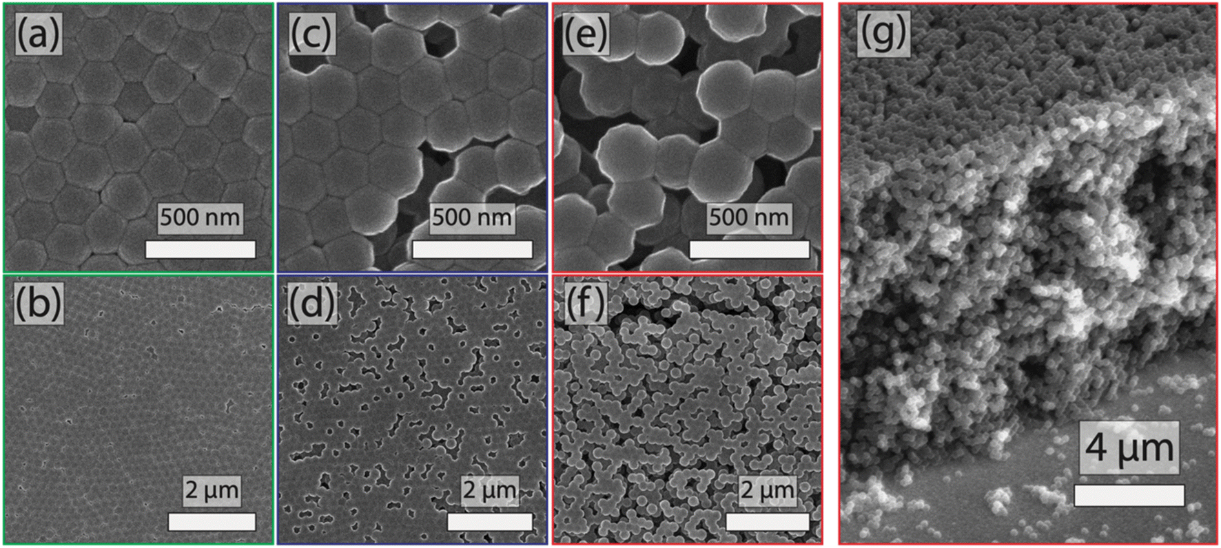 | ||
| Fig. 1 Scanning electron micrographs of a 0% (a and b), a 20% (c and d), and a 50% (e and f) omission glass photoelectrode composed of 200 nm SiO2 nanospheres and a 20 nm layer of TiO2. (g) A side-on image of the 50% omission glass photoelectrode, indicating that the structure was roughly 15 μm thick. | ||
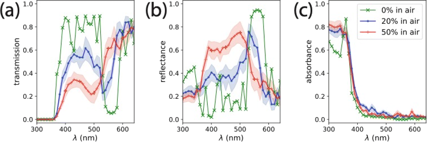
We characterized the absorption of the TiO2 omission glass photoelectrodes using UV-vis diffuse spectroscopy with an integrating sphere. X-ray diffraction measurements showed that the as prepared TiO2 layer was amorphous and formed the anatase phase after annealing at 500 °C (Fig. S1†). Parasitic absorption has been observed in TiO2 films grown by ALD at these temperatures and is attributed to the presence of incompletely decomposed ALD precursor.9,31 We observed this parasitic absorption in the as-prepared films as well (Fig. S2†). The absorption spectra for the annealed omission glass photoelectrodes are shown in Fig. 2. After annealing the photoanodes, the TiO2 coatings crystallized into the anatase phase, and the remaining organic material was removed. The 0%, 20%, and 50% omission electrodes showed negligible transmission and reflectance-limited absorption for wavelengths smaller than the absorption onset of TiO2 (λ < 400 nm). The difference in absorption for λ < 400 nm was increased slightly in the omission glasses (58%, 68%, and 78% at 365 nm in the 0%, 20%, and 50% omission glass electrodes, respectively). As the transmission for each omission glass was effectively zero at these wavelengths (Fig. 2a), the difference resulted from a shift in the reflectance resonance near the absorption onset. The resonance (Fig. 2b) is a maximum at λ = 370 nm for 0% omission (indicated by a green arrow), while the maximum shifts to λ = 400 nm for 50% omission (indicated by a red arrow). The shift in this resonance accounts for the observed increase in absorption near the absorption edge of TiO2 with increasing omission (Fig. 2c). The visible light absorption (λ > 390 nm) in the planar TiO2 layer was identical to the FTO substrate, as would be expected for a TiO2 film lacking chemical defects or dopants. However, the visible absorption in the omission glass electrodes was still higher than the FTO substrate baseline. It is not possible to determine whether this is an artifact of the UV-vis measurement (e.g., light leaking through the edges of the structure and not collected by the integrating sphere, with the measurement geometry shown in Fig. S7†) or some residual parasitic absorption in the anatase TiO2 or FTO layer. The ZnO deposition (50 ALD cycles) used to bind the SiO2 nanospheres together during the omission procedure gave a negligible contribution to the optical properties of the omission glass. Additionally, the ZnO is not in electrical series with the TiO2 except at the base of the structure and had negligible photoelectrochemical effect as well. Photoelectrochemical characterization of ZnO/TiO2 planar photoanodes are included in the ESI (Fig. S10).†
 | ||
| Fig. 2 UV-vis diffuse (a) transmission, (b) reflectance, and (c) absorption spectra of the annealed 0% (green), 20% (blue) and 50% (red) anatase TiO2 omission glass electrodes shown in Fig. 1. Absorption spectra of a planar, 20 nm anatase TiO2 layer (500 ALD cycles) on FTO (purple) and the FTO substrate alone (black) are included for comparison. The reflectance resonances that account for the absorption differences between the 0% and 50% omission glass electrodes are indicated by respectively by a green and red arrow. | ||
We tracked the emergence of the resonances in the 50% omission glass photoelectrode by measuring the diffuse reflectance spectrum at each step of the synthesis (Fig. 3). The substrate reflectance (Fig. 3a) showed the thin film oscillations corresponding to the FTO coating (roughly 330 nm thick, per supplier) on the flat glass substrate. We observed a peak in the reflectance spectra at λ = 460 nm in the as-assembled composite structure (Fig. 3b) and after 50 cycles of ZnO was deposited to bind the SiO2 network together (Fig. 3c). This peak is the stop band due to the crystallinity of the self-assembled composite and was visible by eye as a faint, blue opalescence. The periodic structure and the corresponding stop band reflectance feature were disrupted by removing the PS through a high-temperature annealing step (Fig. 3d). A 20 nm TiO2 layer was then deposited by ALD over the remaining SiO2 nanosphere network. Two new resonant features were observed in the reflectance spectra at λ = 385 nm and at λ = 500 nm (Fig. 3e). The reflectance increased after the TiO2 was annealed to the anatase phase (Fig. 3f) due to the elimination of the visible light absorption in the as-prepared TiO2. The emergent resonances observed after adding the TiO2 layer was distinct from the opalescence of the composite colloidal crystal. The observed resonances came from multiple scattering in the functionalized, disordered nanostructure and therefore can be referred to as resonant multiple scattering. Similar observations have been reported in transmission optical spectroscopy of films of disordered TiO2 nanoparticles.22 It has also been cited as a light trapping strategy in dye-sensitized solar cells, though with limited characterization of the optical properties of the resonant transport.28 The omission glass structure allows for tailorable control of the dielectric contrast through both the omission process and the precise coating properties facilitated by the ALD coating process.
 | ||
| Fig. 3 UV-vis diffuse reflectance spectra of a 50% omission glass photoelectrode at each step of the synthesis: (a) the fluorine-doped tin oxide (FTO)-coated substrate, (b) the self-assembled polystyrene (PS)–SiO2 nanosphere composite, (c) the same composite after ZnO was deposited on the SiO2 by ALD, (d) the composite after removal of the PS nanospheres, (e) after 500 cycles (20 nm) of TiO2 was deposited by ALD on the remaining SiO2 structure, and (f) after the TiO2 layer was annealed to form the anatase phase. | ||
We used finite difference time-domain (FDTD) simulations to characterize the distribution of absorption through an omission glass photoelectrode as a function of the omission percentage.32,33 While the experimental absorption spectra show an increase near the TiO2 absorption edge as the omission percentage increases from 0% to 50% (Fig. 2), there are factors which may impact the usefulness of this absorption for PEC applications. One is that the increase in observed absorption is related to increased light propagation in directions that are not captured in the integrating sphere measurements – transverse ‘leaking’ from the electrode sides, for example, would be uncounted in diffuse reflectance or transmission measurements. Another issue is that the optical density of the omission glass is decreasing with increasing omission percentage. This would suggest that the penetration of light, and hence the average absorption depth, also increases with increasing omission percentage. The steady-state carrier yield would then be affected by the characteristic absorption depth due to limited mass transport through the porous electrode structure. We used FDTD to characterize the macroscopic transmission and reflectance spectra and the microscopic distribution of light absorption. We simulated structures of identical composition for 0%, 20%, and 50% omission in 16-layer omission glass structures (∼2.6 μm thick) based on a 200 nm SiO2–PS omission glass coated with a 20 nm conformal layer of TiO2. Details of the simulations performed here are included in the ESI.† Index of refraction and extinction coefficients (Fig. S4†) for TiO2,34 a transparent conducting oxide,35 and glass/SiO2 (ref. 36) were taken from literature measurements collected in a publicly-available database.37
FDTD-derived transmission, reflection, and absorption spectra for relevant omission glass structures in air is shown in Fig. 4. The 0% omission glass structure is a definite structure, so only one simulation was required to characterize its optical properties. We observed significant reflectance (up to 0.42) in the near-UV, suggesting an absorption-damped stop band in this region. This demonstrates the significance for the choice of the 200 nm colloidal lattice for the TiO2 omission glass photoelectrode – the absorption edge of TiO2 is aligned with the stop band edge of the non-absorbing structure. The 0% omission glass has a second stop band between 530–590 nm, where the extinction coefficient, k(λ), is negligible for real TiO2. Simulated reflectance spectra of 0% omission glass structures showed that increasing the TiO2 thickness beyond 20 nm had little effect on the position of the observed stop band (Fig. S6†). The spectra averaged from the simulations of seven unique 20% omission glass structures show a similar stop band to the 0% omission electrode in that region of the spectrum, but decreased reflectance and lower transmission near the TiO2 absorption edge. The spectra averaged from seven simulations of unique 50% omission glass structures showed a shift in stop band in the visible region to lower λ (500–560 nm). Additionally, the reflectance increased near the TiO2 absorption edge, suggesting the emergence of a modified slow light mode in that structure. The position and intensity of the features in the FDTD simulations of the 50% omission glass structures are consistent with those observed in the reflectance spectrum of a 50% omission photoelectrode (Fig. 2c). When we performed FDTD simulations with the void space infiltrated by water (n = 1.33) rather than air, we observed a slight red shift in the positions of the reflectance features (Fig. S8†). However, the inclusion of water resulted in negligible differences in the absorption spectrum for each structure. For reference, the absorption at 365 nm in each simulation was between 65% and 80% of the incident intensity.
 | ||
| Fig. 4 (a) Transmission, (b) reflectance, and (c) absorption spectra for omission glass photoelectrodes infiltrated by air (n = 1.0) calculated from FDTD simulations. The 0% omission glass (green, ‘×’) is a structure with a definite unit cell, and required only one simulation. The 20% (blue, ‘●’) and 50% (red, ‘+’) omission glasses are disordered with spheres removed at random, each spectrum was averaged from seven different simulations with noted error bars calculated from the standard deviation of these simulations. For comparison, the spectra for infiltration with air versus water (n = 1.33) is shown in Fig. S8.† | ||
We also compared the depth distribution of absorption as a function of the degree of omission for 365 nm illumination (Fig. 5). The resonant transport would be ineffective for PEC photoelectrodes if light absorption occurred in depths of the structure where it was difficult to maintain sufficient reactant transport. For this comparison, we integrated the absorption profile of each simulation in 200 nm segments through the depth of the omission glass electrode. Water (n = 1.33) was used as the infiltrating phase here to simulate the relevant photoelectrochemical environment. The simulation set (λ = 365 nm incident wavelength) comprised one 0% omission, 67 unique 20% omission, and 101 unique 50% omission glass structures. We observed that the partial absorption profile was slightly higher in the first two layers of the 20% omission (0.115 ± 0.010) and 50% omission (0.104 ± 0.015) electrodes than for the 0% omission electrode (0.095). The cumulative absorption in the 0% omission electrode was lower on average than either of the other structures in the top 1.2 μm of each electrode. However, the cumulative absorption in the 0% omission electrode (80%) was higher than either the 20% omission (77%) or the 50% omission (66%) ones. While there was a decrease in the total semiconductor volume with increasing degree of omission for the values studied here, the depth profile of absorption was roughly the same for each degree of omission tested here. Hence, the profile of photocarrier generation should have the same depth dependence.
 | ||
| Fig. 5 (Top) A schematic of the FDTD simulation geometry. A more detailed schematic and an example of simulation data is shown in Fig. S3 and S5 in the ESI.† (Bottom) The integrated absorption of 365 nm illumination (left) in 200 nm slices through the layers of the omission glass photoelectrode structure as a function of omission. The cumulative absorption (dashed lines, right) shows the total percentage of integrated light absorption as a function of depth in the material. The 0% omission data was calculated from a single simulation because there is a single structure in that ensemble. The 20% omission and the 50% omission data were calculated from 67 and 101 unique simulations, respectively, of random structures in each ensemble. The profiles from each spectrum are included as transparent lines under the average profiles. The structures were infiltrated by water (n = 1.33) in these simulations. | ||
We then characterized resonant multiple scattering effects for water oxidation for TiO2-based omission glass photoanodes. Fig. 6a shows CV measurements of PEC water oxidation under LED illumination (λ = 365 nm, 1100 mW cm−2) in 0.1 M KOH for the series of omission glass photoelectrode structures shown in Fig. 1. We chose this high intensity illumination to generate current densities relevant to solar fuels applications (roughly 10 mA cm−2).38 This allows relevant electrochemical effects such as mass transport limitations to be represented in the experiments. For comparison, we included an identically prepared, 20 nm planar TiO2 photoanode on FTO to emphasize the effect of the omission glass structure. The photocurrent measured on the planar TiO2 was 0.27 mA cm−2 at 1.57 V vs. RHE, which can be explained by the combination of low absorption in the thin film (Fig. 2c) and the intrinsic low quantum yield of TiO2 for oxidation reactions without a cocatalyst.39 The absorption increased significantly for all omission glass photoelectrodes, and we observed a corresponding increase in the photocurrent. While the absorption increased by a small percentage with increasing omission percentage (Fig. 2c), the photocurrent increased by a larger factor: from 3.25 mA cm−2 at E = 1.57 V vs. RHE on the 0% omission photoelectrode to 7.47 mA cm−2 and 11.5 mA cm−2 at the same potential for the 20% and 50% omission photoelectrodes, respectively. This is summarized by calculating the external quantum yield (EQY) as a function of intensity from the most positive potentials measured (E = 1.57 V vs. RHE) on three identically prepared photoelectrodes (Fig. 6b). The EQY and its variance increased with increasing omission percentage, from a maximum of 1.3% ± 0.1% for the 0% omission photoelectrode to 5.8% ± 1.6% for the 50% omission photoelectrode at 500 mW cm−2. We observed that the EQY decreased slightly at the highest intensities measured on the 20% and 50% omission photoelectrodes compared to their maximum values. Chronoamperometry (CA) profiles averaged over three measurements on identically prepared photoelectrodes (Fig. 6c) showed that the photocurrents on the 0% omission and 20% omission electrodes reached a steady state value within a few seconds. The average photocurrent on the 50% omission electrode decayed to a steady state value over the course of roughly 200 s and lost nearly a quarter of the initial photocurrent, from an initial value of 11.5 mA cm−2 to roughly 9.0 mA cm−2. The initial photocurrent and decay time varied somewhat, but the qualitatively slow decay and magnitude of the decay was consistent for each set of identically prepared electrodes. Extended CA measurements of omission glass photoelectrodes showed steady, reproducible photocurrents for 60 minutes (Fig. S11†).
 | ||
| Fig. 6 (a) j–E curves for 0% (green), 20% (blue) and 50% (red) porous omission glass electrodes and a planar, annealed 20 nm ALD-TiO2 electrode (purple) in 0.1 M KOH. The solid line CV curves were measured under illumination from a 365 nm LED at 1100 mW cm−2. The dashed line CV curves were measured in the absence of this illumination. The photocurrents obtained in the dark are indistinguishable from zero at this scale (Fig. S9†). (b) External quantum yield of water oxidation on omission glass electrodes at varying 365 nm LED intensity. (c) CA measurements on a 0% (green), 20% (blue) and 50% (red) porous omission glass electrodes in 0.1 M KOH at 1.7 V vs. RHE under illumination from a 365 nm LED at 1100 mW cm−2. Each solid line and ribbon represent the average and standard deviation of CA measurements from three identically prepared electrodes. Current density was normalized to the projected geometric area of the photoelectrode. | ||
We compared the asymptotic behavior of the photocurrent of a 50% omission electrode under frontside and backside (through the transparent FTO substrate) illumination as a function of intensity. The results of the FDTD simulations (Fig. 5) suggested that a significant fraction of the absorption occurs within the first few microns of the omission glass, so backside illumination should generate most of the carriers near the FTO substrate. The omission glass structure between the region absorbing light and the bulk electrolyte would then to impede mass transport to the regions of high carrier generation. The results of this experiment on a single 50% omission glass electrode are shown in Fig. 7. The area of the front side of photoelectrode was defined by epoxy. The backside area was defined by matching the epoxied area with electroplaters tape, which was opaque to 365 nm illumination as confirmed by UV-vis spectroscopy. At the lowest intensity (100 mW cm−2), photocurrent from the front side and back side illumination was indistinguishable, with an asymptotic value of 1 mA cm−2. The asymptotic photocurrent values increased with increasing intensity and were the same for frontside and backside illumination (4.4 mA cm−2 for 500 mW cm−2 and 8.1 mA cm−2 for 1100 mW cm−2). However, the initial photocurrents were slightly lower. The decay time to reach the steady state was only a few seconds for the backside illumination, much shorter than for the frontside illumination on the same electrode at these intensities (40 s for 500 mW cm−2, 260 s for 1100 mW cm−2). This suggests that the reduction in photocurrent on the 50% omission photoelectrode over time is related to mass transport limitations within the interior of the electrode. The backside illumination reached the asymptotic limit more rapidly, but eventually even the electrode illuminated from the front side shows the same mass transport limited photocurrent.
 | ||
| Fig. 7 CA measurements of a 50% omission electrode in 0.1 M KOH at E = 1.7 V vs. RHE under various illumination intensities from a 365 nm LED. Lines with solid circles indicate illumination from the front side of the electrode, and lines with ‘×’ indicate illumination from the back side of the electrode. | ||
The results described here demonstrate that the RMS effect can be deliberately instigated in an omission glass photoelectrode to improve yield for photoelectrochemical reactions. While small light absorption improvements were observed by increasing the degree of omission, both simulations and experimental data establish that light absorption is insufficient to account for the observed increases in photocurrent. Most of the photocurrent enhancement results from allowing the electrolyte to access the internal surface area of the photoelectrode. This combination of improved light absorption and increased electrochemically active surface area result in the observed increases in photocurrents and EQY for the water oxidation reaction studied here. The results are likely generalizable to other photoelectrochemical reactions and semiconductors as well, where carrier generation, recombination, and mass transport of reactants and products are general issues for high-yield PEC energy conversion.
Given the complexity of the overall PEC reaction, it is somewhat surprising that the EQY metric was relatively consistent for the range of intensities studied here. EQY has several components that can be affected by the light intensity. The photovoltage generated in the photoelectrode increases with increasing photocurrent, which essentially increases the overpotential applied to drive the reaction.38 The temperature of the interface can also increase due to the dissipation of heat into the environment. There are also kinetic limitations for any interface, where the reaction mechanism (e.g., electron transfer or chemisorption of reactants) generates an intrinsic limit for current density at a given electrode potential. Explicit mass transport (in the case of a reversible redox reactant) or a pH dependence on the intermediate formation (in the case of water oxidation on TiO2 (ref. 40 and 41)) can limit the PEC reaction in a non-uniform way throughout the interior of a structured electrode. The portion of the electrode that is not absorbing light may act to buffer the kinetic or mass transport limitations of regions in the electrode where photocarriers are generated. The interconnected nature of the interface may facilitate the migration of photogenerated carriers to fresh, underilluminated surfaces with access to reactants. Further studies could investigate the effect that the dark portion of the electrode has on the overall PEC reaction.
The observed difference between the initial and the steady-state, asymptotic photocurrents suggests that mass transport into the interior volume of the electrode remains an issue for improving the photoelectrode performance. The specific omission glass structures studied here were not chosen to optimize the entire multistep transport processes of the full photoelectrochemical reaction. The nanosphere diameter (200 nm) used for developing the nanostructures in this work was chosen with the intention of trapping near-UV light into the TiO2 light absorber. Larger nanospheres would have been chosen to improve visible light trapping relevant to solar-driven applications. The discrete porosity generated by removing 200 nm spheres is likely the source of the mass transport limitations we observed in the 50% porous electrode, for example. The ability to tailor the RMS effect is an appealing strategy for instigating light trapping in a simple-to-fabricate photoelectrode design. Larger pores (e.g., larger polystyrene microspheres) or even hierarchical, multiscale composites may be useful for improving the mass transport through the electrode structure, though the effects on optical transport should be considered for further study. Additionally, the methods used to synthesize the photoelectrodes in this work (e.g., slow evaporation of colloidal suspensions, ALD for material synthesis) can potentially be exchanged for more scalable and tailorable approaches. The integration of semiconductors that can absorb visible light, the identification of scalable composite synthesis strategies, and Multiphysics characterization of the mass transport through the electrode are important next steps in the development of RMS as a light-trapping scheme for photoelectrode design.
Conclusion
In conclusion, we have demonstrated that resonant multiple scattering can be induced in the omission glass photoelectrode structure. The combined effect of light trapping and increased electrochemically active surface area generated by the omission process resulted in improved carrier collection yields in PEC water oxidation. The self-assembly method for synthesis combined with selective ALD processes allow for tailorable porosity, which can be used to tune light absorption, photoelectrochemically active surface area, and mass transport of bulk electrolyte. Increasing the porosity in omission glass photoelectrodes to the degree studied here showed enhancements of up to a 50-fold improvement over an otherwise identically prepared planar ultra-thin film electrode. Hence, resonant multiple scattering is a practicable light trapping strategy for PEC energy conversion. PEC characterization showed that this can be attributed mostly to enhanced activity from within the interior of the electrode structure, and mass transport losses were observed in the omission glass photoelectrodes under steady state operation. These results suggest that to improve the overall photoelectrode performance, the resonant multiple scattering effects should be coordinated with other strategies to optimize the light, chemical, and electronic transport characteristics simultaneously.Data availability
The data and methods that support the findings of this study are included in the ESI† of this article.Author contributions
Ashlyn G. DesCarpentrie: data curation; formal analysis; investigation; methodology; validation; visualization; writing – original draft; writing – review & editing. Robert H. Coridan: conceptualization; data curation; formal analysis; investigation; methodology; resources; software; supervision; validation; visualization; writing – original draft; writing – review & editing.Conflicts of interest
There are no conflicts of interest to declare.Acknowledgements
We acknowledge Dr Mya Norman and Dr Adam Nielander for helpful conversations on this work. This material is based upon work supported by the U.S. Department of Energy, Office of Science, Office of Basic Energy Sciences under award number DE-SC-0020301.References
- M. X. Tan, P. E. Laibinis, S. T. Nguyen, J. M. Kesselman, C. E. Stanton and N. S. Lewis, Principles and Applications of Semiconductor Photoelectrochemistry, in Progress in Inorganic Chemistry, ed. K. D. Karlin, John Wiley & Sons, Inc., 1994, vol. 41, pp. 21–144, DOI:10.1002/9780470166420.ch2.
- M. G. Walter, E. L. Warren, J. R. McKone, S. W. Boettcher, Q. Mi, E. A. Santori and N. S. Lewis, Solar Water Splitting Cells, Chem. Rev., 2010, 110(11), 6446–6473, DOI:10.1021/cr1002326.
- S. B. Mallick, M. Agrawal and P. Peumans, Optimal Light Trapping in Ultra-Thin Photonic Crystal Crystalline Silicon Solar Cells, Opt. Express, 2010, 18(6), 5691–5706, DOI:10.1364/OE.18.005691.
- V. E. Ferry, M. A. Verschuuren, M. C. van Lare, R. E. I. Schropp, H. A. Atwater and A. Polman, Optimized Spatial Correlations for Broadband Light Trapping Nanopatterns in High Efficiency Ultrathin Film a-Si:H Solar Cells, Nano Lett., 2011, 11(10), 4239–4245, DOI:10.1021/nl202226r.
- H. Dotan, O. Kfir, E. Sharlin, O. Blank, M. Gross, I. Dumchin, G. Ankonina and A. Rothschild, Resonant Light Trapping in Ultrathin Films for Water Splitting, Nat. Mater., 2013, 12(2), 158–164, DOI:10.1038/nmat3477.
- D. van der Woude, L. van der Krabben, G. Bauhuis, M. van Eerden, J. J. Kim, P. Mulder, J. Smits, E. Vlieg and J. Schermer, Ultrathin GaAs Solar Cells with a High Surface Roughness GaP Layer for Light-Trapping Application, Prog. Photovoltaics Res. Appl., 2022, 30(6), 622–631, DOI:10.1002/pip.3534.
- H. Liu, Y. Du, X. Yin, M. Bai and W. Liu, Micro/Nanostructures for Light Trapping in Monocrystalline Silicon Solar Cells, J. Nanomater., 2022, 2022(1), 8139174, DOI:10.1155/2022/8139174.
- J. Grandidier, D. M. Callahan, J. N. Munday and H. A. Atwater, Light Absorption Enhancement in Thin-Film Solar Cells Using Whispering Gallery Modes in Dielectric Nanospheres, Adv. Mater., 2011, 23(10), 1272–1276, DOI:10.1002/adma.201004393.
- R. Cherry, J. J. Muhanga, H. Mehrabi, S. K. Conlin and R. H. Coridan, Monolithic Light Concentration by Core–Shell TiO2 Nanostructures Templated by Monodisperse Polymer Colloidal Monolayers, Nanotechnology, 2023, 34(34), 345601, DOI:10.1088/1361-6528/acd787.
- M. Skorobogatiy and J. Yang, Fundamentals of Photonic Crystal Guiding, Cambridge University Press, 2009 Search PubMed.
- J. D. Joannopoulos, S. G. Johnson, J. N. Winn and R. D. Meade, Photonic Crystals: Molding the Flow of Light, Princeton University Press, 2nd edn, 2011 Search PubMed.
- B. M. Kayes, H. A. Atwater and N. S. Lewis, Comparison of the Device Physics Principles of Planar and Radial p-n Junction Nanorod Solar Cells, J. Appl. Phys., 2005, 97(11), 114302, DOI:10.1063/1.1901835.
- J. W. Galusha, C.-K. Tsung, G. D. Stucky and M. H. Bartl, Optimizing Sol–Gel Infiltration and Processing Methods for the Fabrication of High-Quality Planar Titania Inverse Opals, Chem. Mater., 2008, 20(15), 4925–4930, DOI:10.1021/cm800072j.
- F. Sordello, V. Maurino and C. Minero, Photoelectrochemical Study of TiO2 Inverse Opals, J. Mater. Chem., 2011, 21(47), 19144–19152, 10.1039/C1JM12674A.
- M. Wu, J. Jin, J. Liu, Z. Deng, Y. Li, O. Deparis and B.-L. Su, High Photocatalytic Activity Enhancement of Titania Inverse Opal Films by Slow Photon Effect Induced Strong Light Absorption, J. Mater. Chem. A, 2013, 1(48), 15491–15500, 10.1039/C3TA13574H.
- M. Ma, J. K. Kim, K. Zhang, X. Shi, S. J. Kim, J. H. Moon and J. H. Park, Double-Deck Inverse Opal Photoanodes: Efficient Light Absorption and Charge Separation in Heterojunction, Chem. Mater., 2014, 26(19), 5592–5597, DOI:10.1021/cm502073d.
- M. Curti, J. Schneider, D. W. Bahnemann and C. B. Mendive, Inverse Opal Photonic Crystals as a Strategy to Improve Photocatalysis: Underexplored Questions, J. Phys. Chem. Lett., 2015, 6(19), 3903–3910, DOI:10.1021/acs.jpclett.5b01353.
- E. Armstrong and C. O'Dwyer, Artificial Opal Photonic Crystals and Inverse Opal Structures – Fundamentals and Applications from Optics to Energy Storage, J. Mater. Chem. C, 2015, 3(24), 6109–6143, 10.1039/C5TC01083G.
- A. Maho, M. Lobet, N. Daem, P. Piron, G. Spronck, J. Loicq, R. Cloots, P. Colson, C. Henrist and J. Dewalque, Photonic Structuration of Hybrid Inverse-Opal TiO2—Perovskite Layers for Enhanced Light Absorption in Solar Cells, ACS Appl. Energy Mater., 2021, 4(2), 1108–1119, DOI:10.1021/acsaem.0c02124.
- M. T. Spitler, M. A. Modestino, T. G. Deutsch, C. X. Xiang, J. R. Durrant, D. V. Esposito, S. Haussener, S. Maldonado, I. D. Sharp, B. A. Parkinson, D. S. Ginley, F. A. Houle, T. Hannappel, N. R. Neale, D. G. Nocera and P. C. McIntyre, Practical Challenges in the Development of Photoelectrochemical Solar Fuels Production, Sustainable Energy Fuels, 2020, 4(3), 985–995, 10.1039/C9SE00869A.
- G. Segev, J. Kibsgaard, C. Hahn, Z. J. Xu, W.-H. Cheng, T. G. Deutsch, C. Xiang, J. Z. Zhang, L. Hammarström, D. G. Nocera, A. Z. Weber, P. Agbo, T. Hisatomi, F. E. Osterloh, K. Domen, F. F. Abdi, S. Haussener, D. J. Miller, S. Ardo, P. C. McIntyre, T. Hannappel, S. Hu, H. Atwater, J. M. Gregoire, M. Z. Ertem, I. D. Sharp, K.-S. Choi, J. S. Lee, O. Ishitani, J. W. Ager, R. R. Prabhakar, A. T. Bell, S. W. Boettcher, K. Vincent, K. Takanabe, V. Artero, R. Napier, B. R. Cuenya, M. T. M. Koper, R. Van De Krol and F. Houle, The 2022 Solar Fuels Roadmap, J. Phys. D: Appl. Phys., 2022, 55(32), 323003, DOI:10.1088/1361-6463/ac6f97.
- M. P. van Albada, B. A. van Tiggelen, A. Lagendijk and A. Tip, Speed of Propagation of Classical Waves in Strongly Scattering Media, Phys. Rev. Lett., 1991, 66(24), 3132–3135, DOI:10.1103/PhysRevLett.66.3132.
- D. S. Wiersma, Disordered Photonics, Nat. Photonics, 2013, 7(3), 188–196, DOI:10.1038/nphoton.2013.29.
- N. Granchi, R. Spalding, K. Stokkereit, M. Lodde, M. Petruzzella, F. V. Otten, R. Sapienza, A. Fiore, M. Florescu and F. Intonti, High Spatial Resolution Imaging of Light Localization in Hyperuniform Disordered Patterns of Circular Air Pores in a Dielectric Slab, Front. Photonics, 2023, 4, 1199411, DOI:10.3389/fphot.2023.1199411.
- G. J. Aubry, L. S. Froufe-Pérez, U. Kuhl, O. Legrand, F. Scheffold and F. Mortessagne, Experimental Tuning of Transport Regimes in Hyperuniform Disordered Photonic Materials, Phys. Rev. Lett., 2020, 125(12), 127402, DOI:10.1103/PhysRevLett.125.127402.
- D. Chen, H. Zhuang, M. Chen, P. Y. Huang, V. Vlcek and Y. Jiao, Disordered Hyperuniform Solid State Materials, Appl. Phys. Rev., 2023, 10(2), 021310, DOI:10.1063/5.0137187.
- A. Lagendijk and B. A. van Tiggelen, Resonant Multiple Scattering of Light, Phys. Rep., 1996, 270(3), 143–215, DOI:10.1016/0370-1573(95)00065-8.
- J. Kim, H. Lee, D. Y. Kim and Y. Seo, Resonant Multiple Light Scattering for Enhanced Photon Harvesting in Dye-Sensitized Solar Cells, Adv. Mater., 2014, 26(30), 5192–5197, DOI:10.1002/adma.201400124.
- M. A. Norman, W. L. Perez, C. C. Kline and R. H. Coridan, Enhanced Photoelectrochemical Energy Conversion in Ultrathin Film Photoanodes with Hierarchically Tailorable Mesoscale Structure, Adv. Funct. Mater., 2018, 28(29), 1800481, DOI:10.1002/adfm.201800481.
- P. J. Reed, H. Mehrabi, Z. G. Schichtl and R. H. Coridan, Enhanced Electrochemical Stability of TiO2-Protected, Al-Doped ZnO Transparent Conducting Oxide Synthesized by Atomic Layer Deposition, ACS Appl. Mater. Interfaces, 2018, 10(50), 43691–43698, DOI:10.1021/acsami.8b16531.
- M.-J. Kim, J.-S. Bae, M.-J. Jung, E. Jeon, Y. Park, H. Khan and S.-H. Kwon, Atomic Layer Deposition of Defective Amorphous TiOx Thin Films with Improved Photoelectrochemical Performance, ACS Appl. Mater. Interfaces, 2023, 15(39), 45732–45744, DOI:10.1021/acsami.3c06780.
- A. F. Oskooi, D. Roundy, M. Ibanescu, P. Bermel, J. D. Joannopoulos and S. G. Johnson, Meep: A Flexible Free-Software Package for Electromagnetic Simulations by the FDTD Method, Comput. Phys. Commun., 2010, 181(3), 687–702, DOI:10.1016/j.cpc.2009.11.008.
- A. Taflove and S. C. Hagness, Computational Electrodynamics, Artech House, Boston, MA, 3rd edn, 2005 Search PubMed.
- T. Siefke, S. Kroker, K. Pfeiffer, O. Puffky, K. Dietrich, D. Franta, I. Ohlídal, A. Szeghalmi, E.-B. Kley and A. Tünnermann, Materials Pushing the Application Limits of Wire Grid Polarizers Further into the Deep Ultraviolet Spectral Range, Adv. Opt. Mater., 2016, 4(11), 1780–1786, DOI:10.1002/adom.201600250.
- S. Goldsmith, E. Çetinörgü and R. L. Boxman, Modeling the Optical Properties of Tin Oxide Thin Films, Thin Solid Films, 2009, 517(17), 5146–5150, DOI:10.1016/j.tsf.2009.03.019.
- I. H. Malitson, Interspecimen Comparison of the Refractive Index of Fused Silica, J. Opt. Soc. Am., 1965, 55(10), 1205–1209, DOI:10.1364/JOSA.55.001205.
- M. N. Polyanskiy, Refractiveindex.Info Database of Optical Constants, Sci. Data, 2024, 11(1), 94, DOI:10.1038/s41597-023-02898-2.
- R. H. Coridan, A. C. Nielander, S. A. Francis, M. T. McDowell, V. Dix, S. M. Chatman and N. S. Lewis, Methods for Comparing the Performance of Energy-Conversion Systems for Use in Solar Fuels and Solar Electricity Generation, Energy Environ. Sci., 2015, 8(10), 2886–2901, 10.1039/C5EE00777A.
- K. Ishibashi, A. Fujishima, T. Watanabe and K. Hashimoto, Quantum Yields of Active Oxidative Species Formed on TiO2 Photocatalyst, J. Photochem. Photobiol., A, 2000, 134(1), 139–142, DOI:10.1016/S1010-6030(00)00264-1.
- A. Imanishi, T. Okamura, N. Ohashi, R. Nakamura and Y. Nakato, Mechanism of Water Photooxidation Reaction at Atomically Flat TiO2 (Rutile) (110) and (100) Surfaces: Dependence on Solution pH, J. Am. Chem. Soc., 2007, 129(37), 11569–11578, DOI:10.1021/ja073206+.
- Á. Valdés, Z.-W. Qu, G.-J. Kroes, J. Rossmeisl and J. K. Nørskov, Oxidation and Photo-Oxidation of Water on TiO2 Surface, J. Phys. Chem. C, 2008, 112(26), 9872–9879, DOI:10.1021/jp711929d.
Footnote |
| † Electronic supplementary information (ESI) available: Details of synthesis and characterization methods, simulation methods, materials structure and electrochemical characterization. See DOI: https://doi.org/10.1039/d5sc02916c |
| This journal is © The Royal Society of Chemistry 2025 |