
 Open Access Article
 This Open Access Article is licensed under a
 Creative Commons Attribution 3.0 Unported Licence
Challenges and opportunities for the characterization of electronic properties in halide perovskite solar cells
Thomas
Kirchartz
 ab
ab
aIMD-3 Photovoltaics, Forschungszentrum Jülich, 52425 Jülich, Germany
bFaculty of Engineering and CENIDE, University of Duisburg-Essen, Carl-Benz-Str. 199, 47057 Duisburg, Germany. E-mail: t.kirchartz@fz-juelich.de
First published on 29th April 2025
Abstract
Characterisation of the electronic properties of halide perovskites is often a dilemma for researchers. Many of the data analysis methods for the most common techniques in semiconductor device physics have a small validity window or are generally only applicable to classical doped semiconductors. As alternative data analysis approaches are often prohibitively complicated and require numerical simulations of electronic and often ionic charge carriers, the analysis of data is performed qualitatively and comparatively. The overarching idea is that even if data analysis methods do not apply to a given sample, the trend should still be maintained. However, even this last statement may not be correct in certain situations. Hence, the present review provides a summary of the canonical, frequently used methods to characterise electronic properties in halide perovskites and provides a short explanation of the pitfalls in applying the method, as well as the opportunities that arise from using these methods in ways that are not yet common in the current literature.
 Thomas Kirchartz | Thomas Kirchartz is a professor in the Department of Electrical Engineering and Information Technology at the University Duisburg-Essen (since 2013). In addition, he is the head of the Department of Analytics and Simulation and the group for Organic and Hybrid Solar Cells at the Research Centre Jülich (Institute of Energy Materials and Devices). Previously he was a junior research fellow at Imperial College London (2010–2013) and received a Dr-Ing. from RWTH Aachen (2009). His research interests include the fundamental understanding of photovoltaic devices, their characterization and simulation, and the development of solution-processable solar cells. |
1. Introduction
A significant fraction of the work on halide perovskite solar cells is dedicated to improving the performance and stability1–4 of the devices by changing processes,5–7 modifying interfaces,8–12 or choosing suitable transport layers.13–16 As shown in Fig. 1, the improvement in solar cell performance is typically followed by an analysis of the data aimed at correlating the chemistry and structure of the materials and interfaces of the improved solar cell with electronic properties and subsequently with device performance (typically one-sun efficiency). Concerning the characterisation of electronic properties, the research community working on device optimisation has arrived at a clear consensus on the methods used to characterise each of the critical parameters shown in Fig. 1. At the same time, the community working on developing these characterisation methods and associated data interpretation methods has arrived at an entirely different consensus: many of the methods shown in the green parts of Fig. 1 are used and analysed in a way that may lead to erroneous results. Thus, the halide perovskite community is currently in a situation where classical methods of scientific quality control (i.e. mostly peer review) fail, such that a significant fraction of papers, including those in the most reputable journals, include data interpretation that is well understood to be wrong by the subset of the community that works on the data interpretation aspects. This problem is made more severe by the fact that in many cases “wrong” does not mean unprecise but uncorrelated to the quantity in question. In other situations, “wrong” might mean that the data interpretation may or may not be correct; it is impossible to discern from the data. In other words, confidence in the data interpretation approach is low, implying that additional information is required. Given the weak coupling between the subsets of research communities, it might be necessary to discuss known issues with the set of canonical techniques that have been established as the unwritten standard for electronic property characterisation in halide perovskites. Furthermore, I highlight possible alternatives in terms of both the techniques and data analysis methods. | ||
| Fig. 1 Typical flow of a primarily experimental paper that aims at technological improvements within the field of halide perovskite solar cells. Technological innovations are presented, and it is subsequently shown which structural, chemical, optical, and electronic material properties change. Eventually, the full device is characterised, which provides information on its performance and stability. Furthermore, electrical characterisation at the device level may provide further insights into properties such as defect densities, lifetimes, and interface recombination velocities. Abbreviations used: SIMS: secondary ion mass spectroscopy, XPS: X-ray photoelectron spectroscopy, XRD: X-ray diffraction, FTIR: Fourier-transform infrared spectroscopy, SEM: scanning electron microscopy, DFT: density functional theory, UV-vis: transmission and reflection measurements from the ultraviolet to the visible and often near-infrared wavelength range, PDS: photothermal deflection spectroscopy, PLQY: photoluminescence quantum efficiency, tr-PL: transient photoluminescence, UPS: ultraviolet photoelectron spectroscopy, KPFM: Kelvin-probe force microscopy, JV: current–voltage curves, EQE: external quantum efficiency (of a solar cell), SCLC: space charge limited current measurements, TPC & TPV: transient photocurrent & photovoltage. Figures for step 1 & step 2. Reproduced from ref. 5 under the terms of the CC-BY 4.0 license. Copyright the authors of ref. 5 (2023). Figure for step 4: reproduced from ref. 17 under the terms of the CC-BY 4.0 license. Copyright the authors of ref. 17 (2023). | ||
1.1. The canonical techniques
An important question within the context of this article is how research communities arrive at a set of generally approved characterisation techniques that most researchers within the community understand and accept as both valid and useful. I will refer to these techniques within this article as canonical techniques, as they provide something akin to a research-project and paper-writing template for a significant fraction of the research community. For the religions of the book such as Judaism and Christianity, the canonical books are those that have been included in a certain edited volume of religious texts such as the bible. The selection of books that were included or excluded from a volume of religious texts was decided by a select group of people, for instance, by the Council of Rome (382 AD) for the case of the Catholic Bible. Research communities within the field of science and engineering may similarly arrive at a set of accepted wisdom, including accepted characterisation techniques that are considered both useful and sometimes mandatory for certain types of studies. Often, this set of accepted techniques that I refer to in this article as canonical techniques is not selected by groups of individuals but rather develops by interaction of researchers among each other as well as with editors and peer reviewers during the process of publishing a manuscript. Academic research can be thought of as an information network that has – in principle – excellent self-correcting mechanisms18 such as peer review and the possibility to write review articles, perspectives, commentaries on published papers, or discuss questions at conferences. These mechanisms should lead to continuous reassessment of the most suitable techniques for answering a given scientific question. As has been recently proven for certain techniques,19 these self-correcting mechanisms work relatively poorly (for the standards of academia) in the field of halide-perovskite solar cell research that is the subject of the present article.Fig. 1 and Table 1 list a range of methods routinely used to characterise the electronic properties of halide perovskites. These techniques include the use of the trap-filled limit in single-carrier devices (often called space-charge-limited current (SCLC) measurements) and capacitance-based techniques to study defect densities. The defect densities are then correlated with the charge-carrier lifetimes and PL quantum yields, which are typically assessed by transient and steady-state photoluminescence. Often, additional time- or frequency-domain techniques are employed to determine the charge-carrier lifetimes of complete devices. These include transient photovoltage, impedance, and intensity-modulated photocurrent or photovoltage. Occasionally, charge extraction or charge transport is further characterised using methods such as transient photocurrent, transient photoluminescence on bilayers, and recently, voltage-dependent photoluminescence on complete solar cells.
| Quantity | Method | Challenges & risks for misinterpretation |
|---|---|---|
| Defect density | Trap filled current in single carrier devices | Built-in voltage leads to exponential regime20 |
| Capacitance based methods | Electrode charge or injected charge dominates result21 | |
| Lifetime | Transient photoluminescence | Non-exponential decays interpreted with exponential model22 |
| Repetition rate affects result23–25 | ||
| Transient photovoltage | Capacitive effects interpreted as recombination lifetime26 | |
| Impedance | One Nyquist plot at one voltage shown. Insufficient for interpretation of time constant27,28 | |
| Doping | Capacitance, Mott–Schottky | Missing depletion capacitance29 |
| Transition from geometric to chemical capacitance interpreted as doping density21,29 | ||
| Energy levels | Photoelectron spectroscopy | Huge variation in values as a function of analysis method of the band edge30,31 |
| Mobility | SCLC, TPC | Difficult to disentangle the effect of perovskite absorber from that of contact layers30 |
| Photoluminescence | Out-of-plane vs. in-plane mobilities vary by orders of magnitude32 | |
| Charge transfer and extraction | Transient PL on bilayers | Discrimination between recombination and charge transfer difficult33,34 |
| Voltage dependent PL | Difficult to disentangle effects of electron and hole transport layers. Complete device needed |
Problems with the methods for determining defect densities are mostly based on the challenge of measuring the charge of the defects in a situation in which the charge density integrated over the thickness is much smaller than the charge density per area of the electrodes. This requirement leads to a situation in which defects can be measured via their charge only if their density exceeds a certain value that depends on the thickness d of the sample and permittivity ε of the material.
Challenges with determining charge-carrier lifetimes are usually associated with the difficulty in discriminating different transient effects from each other.33,35 Transients in films, layer stacks and devices are typically affected by many different phenomena that include charge trapping/detrapping, recombination, charge transfer and back transfer to other layers,34 capacitive charging/discharging of electrodes,26,36 and ion motion.37–39 Sometimes, the interpretation of the decay time as charge-carrier lifetime is possible while in other situations it is not possible or very difficult.26 Thus, in this context, strategies are necessary to identify confidence in the interpretation of time constants or decay times in terms of one of the previously mentioned physical phenomena.40,41
In this article, I will first discuss some important fundamental concepts underlying many data analysis methods for electrical and optoelectronic measurement techniques in Chapter 2. From Chapter 3 onwards, the article deals with different parameters of interest along the logic of Table 1, discusses the challenges in each chapter in more detail (last column in Table 1), and then highlights opportunities for improvement in the techniques and the respective data analysis approaches. These opportunities may be based on recent research or point towards possible directions for future innovations. The methods that I discuss will be primarily taken from the list of frequently used (i.e. canonical) methods. However, especially where canonical methods fall short of providing answers to the major scientific questions, I will also briefly discuss alternative techniques that may provide solutions for the problems of the more frequently used techniques. While these alternatives are not currently widely used, they may become important in the future if – as I hope – the canon of popular methods gradually shifts towards characterization and data analysis methods that maximize information gain for researchers working in the field.
2. Important concepts
Many concepts for the analysis of experimental data on any type of solar cell are based on the analytical approximations to the continuity equations for electrons and holes as well as the Poisson equation that will be introduced in Chapter 2.1. Analytical approximations are often possible only if one deals with a doped semiconductor, where only the continuity equation of the minority carriers is important. Thus, many of the analytical equations frequently found in the literature on halide perovskite solar cells originate from doped semiconductors, which are often inapplicable to many lead-halide perovskite compositions that frequently show a very low doping density42 and potentially a high density of mobile ions. The following sections allow interested readers to examine some of the concepts mentioned later in the chapters on different measurement techniques.2.1. Drift-diffusion model
The importance of what I will refer to as the electronic properties of semiconductors is their impact on the transport and recombination of charge carriers in semiconducting devices. Material properties, such as the crystallinity and stoichiometry of a chemical compound, can affect transport and recombination,43–45 but these material properties do not directly appear in the equations used to calculate e.g. current–voltage curves of semiconducting devices. Furthermore, processing parameters, such as the viscosity of a solution or the annealing temperature and time, can affect the properties of the resulting device; however, they are not directly featured in the typically used equations. Instead, the electronic properties discussed in this review are properties such as mobility, lifetime, and interface recombination velocity of charge carriers as well as the defect and doping densities, work functions, and energy levels of the semiconductors involved. All these parameters appear directly or indirectly in the three equations used to calculate the carrier and current densities as a function of the external light and voltage bias. This formalism is usually referred to as the drift-diffusion model. The three coupled differential equations46 that are typically solved are the Poisson equation | (1) |
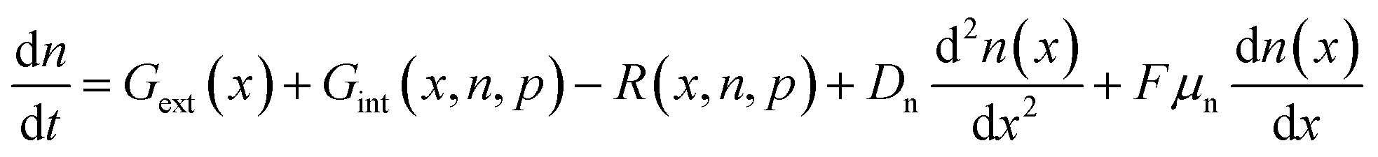 | (2) |
 | (3) |
Eqn (1)–(3) are often solved numerically using so-called drift diffusion solvers (see Table 2) and then provide a solution for n(x, t), p(x, t), and φ(x, t). From the carrier densities, the current densities for electrons and holes follow via
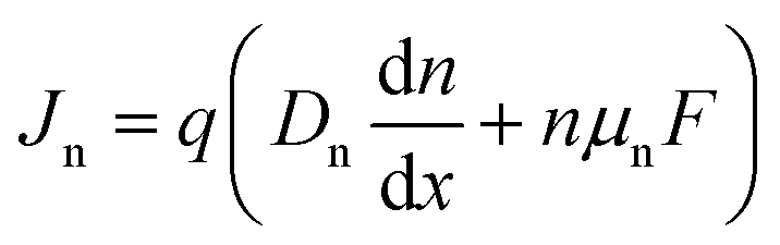 | (4) |
 | (5) |
| Name | URL | Ions included? | Transients | Frequency dependent | Free or commercial |
|---|---|---|---|---|---|
| SETFOS | https://www.fluxim.com/setfos-intro | Yes | Yes | Yes | Comm. |
| SIMsalabim47 | https://github.com/kostergroup/SIMsalabim | Yes | Yes | Yes | Free |
| BOAR & SiMsalabim | https://github.com/i-MEET/boar | Note: Bayesian optimization tool combined with drift-diffusion tool (for fitting and parameter estimation) | |||
| DriftFusion48 | https://github.com/barnesgroupICL/Driftfusion | Yes | Yes | Yes | Free (Matlab based) |
| IonMonger49 | https://github.com/PerovskiteSCModelling/IonMonger | Yes | Yes | Yes | Free (Matlab based) |
| OghmaNano50 | https://www.oghma-nano.com/contact.html | Yes | Yes | Yes | Free |
| SCAPS51,52 | https://scaps.elis.ugent.be/ | No | No | Yes | Free |
| ASA53,54 | https://asa.ewi.tudelft.nl/ | No | No | No | Commercial |
The total current density is then J = Jn + Jp. Alternatively, in any steady state situation, the current densities can also be calculated via integrating over the rates of recombination and generation. In the typical sign convention where the photocurrent is negative and the recombination current is positive, we can write55
 | (6) |
2.2. Ionic–electronic conduction
Halide perovskites have the peculiar property that several of the possible intrinsic defects have a significant diffusion coefficient implying that the material contains charged, mobile defects.62–65 These mobile defects are typically referred to as mobile ions and could be for instance, halide interstitials or halide vacancies. If they are charged, any movement of these intrinsic defects by drift or diffusion will create an ionic current and may change the electrostatics of the device.38,63,66 Thus, ions can have a direct effect on the transient currents measured that would be absent in a purely steady-state situation. However, even in steady state, the ions can change the band diagram as opposed to a situation without ions.67,68 For instance, the movement of negatively charged ions towards the cathode and positively charged ions towards the anode can lead to a screening of the electric field within the perovskite absorber layer. Thus, due to this combination of ionic and electronic conduction in halide perovskites, the drift-diffusion model can be extended to accommodate also the effect of ion movement.63,69 Usually, ions are implemented in such a way that their charge contributes to the charge density ρ in eqn (1) and their movement due to drift or diffusion is added to the electronic current densities in the same way as for electrons and holes. However, there is usually no term for the generation and recombination of ions included, but their overall density is fixed, and the codes then simulate how their density changes as a function of time after some change in condition (i.e. a voltage step during the simulation of a current–voltage curve).Table 2 provides a list of drift-diffusion solvers that are accessible either commercially or for free (via e.g. GitHub repositories) and that are either specifically designed for use with halide perovskites or have been applied to perovskite solar cells in specific situations. The table further provides information on whether the software allows one to simulate ion diffusion, transients, and frequency domain measurements. An exception is the entry for the python code BOAR which creates an interface between a Bayesian optimization algorithm and a drift-diffusion solver (in this case SIMsalabim47), which thereby allows finding parameters for use in a drift-diffusion code based on experimental observations (e.g. current–voltage curves). This implies fitting the output of a drift-diffusion solver to experimental data and thereby inferring unknown material parameters.
2.3. The depletion approximation
The depletion approximation is an important component in the analytical analysis of capacitance measurements and indicates that there is (a) a space-charge region (synonym: depletion region) with a certain width, such that (b) can be assumed to be depleted of free charge carriers. The charge density in the depletion region is then entirely determined by the charge of the ionised dopant atoms. Thus, if we had a p-type semiconductor that has a space-charge region towards a low-workfunction metal, the space charge in the space-charge region would be given by| ρ = q(p − n − NA + ND) ≈ −qNA | (7) |
2.4. The neutral zone
In doped semiconductors, the device can usually be split into a neutral zone and one or two space charge regions. In the neutral zone, the space charge (for example for a p-type semiconductor) is| ρ = q(p − n − NA + ND) ≈ q(p − NA) ≈ 0. | (8) |
Hence, there is no electric field, which allows us to simplify the continuity equation within the neutral zone to the diffusion equation (see Section 2.5) to study transport and recombination. The neutral zone is central to the way Si solar cell device physics is usually explained,71 as in Si solar cells; typically, the space-charge region width is on the order of hundreds of nanometers, while the neutral zone has a typical thickness of 99.9% of the total wafer thickness.
2.5. The Debye length
The Poisson equation (eqn (1)) states that the second spatial derivative of the electrostatic potential is proportional to the space-charge density. Thus, for a given constant space charge density ρ, a certain distance is required for the electrostatic potential to change by a given amount. If we assume this amount to be the thermal voltage kT/q, the distance required is named the Debye length wD and is given by (see p. 85 in ref. 70) | (9) |
The Debye length is closely related to the width of the space-charge region which is given for the example of a p-type semiconductor–metal junction by
 | (10) |
2.6. The charge-carrier lifetime
In physics, many decay processes can be approximated as following the solution to a first order differential equation of the form dn/dt = −n/τ, where n is the decaying species, t is the time and τ is a characteristic time constant. The solution to such an equation is an exponential decay of the form n(t) = n(0)exp(−t/τ). Usually, the parameter τ of these decays has important implications that may range from how well suited a semiconductor is for photovoltaics up to how long one must store radioactive waste. The parameter τ has many names that include decay time, characteristic time constant or lifetime of the species n. For processes that do indeed follow dn/dt = −n/τ to a good approximation, the lifetime is extremely important, useful, and straightforward to understand. Once processes do decay but may not exactly (or even not at all) follow dn/dt = −n/τ, the use and interpretation of the lifetime becomes a challenge of central relevance also to the field of halide perovskites.Within the field of semiconductors, the charge-carrier lifetime is a concept for quantifying the speed of recombination that makes sense in doped semiconductors and semiconductors with deep traps.73 In both cases, decay processes follow dn/dt = −n/τ quite well. Either of the two conditions being fulfilled (doping or deep traps) is a highly relevant scenario for all traditional semiconductors. Thus, the charge-carrier lifetime is nearly omnipresent in the literature on semiconductors. However, this is not an easy-to-use concept for intrinsic semiconductors with shallow traps or band tails, which is often relevant for both lead-halide perovskites and organic semiconductors. To understand the charge-carrier lifetime, we must distinguish between models and quantities derived from experimental data, both of which are often called lifetimes but are not necessarily the same.
2.7. The diffusion length
In the neutral zone of a solar cell based on doped absorber layers, we have a negligibly small electric field, and majority and minority carriers. Thus, in the example of a p-type semiconductor, in the neutral zone, electrons are minority carriers, and only the recombination and transport of electrons affect the open-circuit voltage Voc and short-circuit current density Jsc. The slow transport of majority carriers can cause resistive loss, reducing the fill factor, FF, but it cannot lead to recombination losses. In the neutral zone, eqn (2) simplifies to | (11) |
 | (12) |
 must hold to satisfy eqn (11). Parameters A and B must be determined using appropriate boundary conditions but are not important for the current discussion. The important aspect of eqn (12) is that only the square root of the product of the diffusion coefficient and lifetime controls the spatial dependence of the excess electron concentration and thereby the recombination rate R = Δn/τ. All other parameters that could affect recombination are part of the boundary conditions. Thus, it is a logical concept to use the diffusion length L as a figure of merit for the bulk electronic quality of a doped (!) semiconductor.
3. Defect characterization
Quantifying the densities and energetic or spatial positions of defects is a useful intermediate step in relating the effect of bulk or interface passivation strategies to recombination rates and, eventually, functionality. To measure defects, one requires an observable that serves as a proxy for the actual defect density. The most frequently used proxy for defect density is the bulk charge density72 which is unrelated to the charge of free carriers. If such a charge density can be unambiguously identified, values of defect densities can be inferred at least approximately. Alternatively, defects can be inferred from photoemission signals; that is, if a UV photon can create a free electron above the vacuum level from a certain energetic depth, then one can infer the presence of a near-surface state at a certain energy.16,31 As long as this occurs at an energy within the bandgap, defects near the surface can be identified in such a way.3.1. JV-Curves of single carrier devices
 | ||
| Fig. 2 (a) Current/voltage curves of a device with and without charged acceptor-like defects with a total concentration of NT = 1017 cm−3 and a Gaussian width of σ = 100 meV are compared to the Mott–Gurney law. Band diagrams of device (b) without charged defects and device (c) with charged defects. The acceptor-like defects in (c) create a barrier owing to their negative charge. The diffusion of electrons up the barrier causes a reduction in the current in (a). Figure reproduced from ref. 20 under the terms of the CC-BY 2.0 license. ©2013. The author of ref. 20. | ||
 | ||
| Fig. 3 (a) Current/voltage curves of a device with charged acceptor-like defects and a built-in voltage of Vbi = 0 V (as in Fig. 1a), and a device with no defects but a built-in voltage ofVbi = 1 V are compared to the Mott–Gurney law. Band diagram of device (b) without charged defects and Vbi = 1 V, and (c) with charged defects and Vbi = 0 V. Both band diagrams are depicted at short circuit. Figure reproduced from ref. 20 under the terms of the CC-BY 2.0 license. © 2013. The author of ref. 20. | ||
 | ||
| Fig. 4 Apparent defect densities vs. thickness for (a) single-carrier devices and (b) capacitance–voltage curves of perovskite solar cells (black symbols) and drive-level capacitance profiling data (blue symbols). The lines indicate the minimum volume defect density that should be measurable according to the equations in the figure. Reprinted with permission from ref. 72. © 2021. The authors of ref. 72. | ||
A second noteworthy insight83 was the investigation into the correct feature of the JV curve that should be used to assign the trap-filled voltage to, once the detection-threshold check is positive. Thus, for applications in single crystals, where the sample thickness is high enough for the trap detection method to fundamentally work, there is still the question of how to reliably and accurately determine the trap-filled voltage Vtfl. Often, the first kink (at the lowest voltages) is used in literature. This first kink separates the linear part of the JV curve to the exponentially increasing one that is a signature of the actual trap filling process. The second kink is then the transition from the trap-filled current to the space-charge limited current (J–V2), which is indeed the point that does correlate with the trap density. This, however, means that even for single crystals, the trap density determination requires three regimes to be clearly visible (linear, exponential and quadratic) as only the transition exponential to quadratic contains the information on the overall trap density. For a visual illustration of this message, see for instance the table of contents figure of ref. 19. Further, it is noteworthy that 3 years after the 2021 publication of ref. 83 still 80% of the papers citing (!) ref. 83 use the lower kink in the curve and only 20% use the correct upper kink.19 This means that even though the information is in the literature, and the papers are found and cited, they are still having a moderately low influence on the actual behaviour of the researchers performing and analysing the measurements.
Instead of measuring the defect density, it might be safer to use the measurement of single-carrier devices to map the energy levels and work functions of contacts by comparing forward and reverse bias measurements. In an ideal single-carrier device, both injection barriers are zero. However, the injection barriers are often slightly different, which leads to differences in the current–voltage curves for forward and reverse bias. Röhr recently developed an analytical approach to quantify the electrostatic potential difference between the two electrodes of a single carrier device from the current ratio between forward and reverse bias sweeps.80 As small differences in the injection barriers are visible in the current ratios, the method can be applied to measure the work function differences between different contact layers.30 While the absolute work function is not accessible, the differences are, and these are usually the relevant quantities needed for numerical simulations of devices.
Fig. 5 shows an example of how the choice of electron injection layer affects the JV curves of single-carrier devices. Fig. 5a shows the forward and reverse bias measurements of the glass/ITO/SnO2/perovskite/C60/BCP/Ag device. Fig. 5b shows the experimental ratio between the forward and reverse current densities for different fullerenes with slightly different electron affinities. As fullerenes with higher electron affinities and a larger conduction band offset to the perovskite show higher current ratios, we presume that there is Fermi level pinning at the BCP-fullerene interfaces that leads to higher built-in potential differences in those cases, where the electron affinity is high.
 | ||
| Fig. 5 (a) Dark JV-curves of the electron-only device with C60 as electron transport layer (spheres) and drift-diffusion simulations (solid lines). The lower branch with the arrow to the left is the measurement/simulation from −3 V to 0 V (reverse current Jr), and the upper branch with the arrow to the right represents the measurement/simulation from 0 V to 3 V (forward current Jf). (b) Logarithm of the ratio Jf/Jr calculated from measurements of electron-only devices with different fullerenes (spheres). Redrawn from ref. 30 under the terms of the CC-BY 4.0 license. © 2023. The authors of ref. 30. | ||
3.2. Capacitance-based techniques
 | ||
| Fig. 6 (a) Simulated Mott–Schottky plot of an intrinsic perovskite solar cell that shows a transition from a voltage-independent geometrical capacitance at reverse and low forward bias (red) to a higher capacitance at forward bias owing to charge injection (blue). The transition region (green) is frequently misinterpreted as a region indicative of the depletion capacitance, and hence, the doping density. (b) Apparent charge density resulting from the slope of the curve in (a) plotted as a function of voltage. (c) Apparent charge density resulting from the slope of the curve in (a) plotted as a function of x position. The figure was reproduced with permission from ref. 21. © The American Association for the Advancement of Science, 2021. | ||
A second challenge in understanding the shape of the capacitance–voltage curves is the debated origin of the forward bias capacitance, which leads to the inflection point in Fig. 6a and the U-shape in Fig. 6c. There are several reasons why the capacitance can increase at a forward bias. The implicitly assumed reason in the logic of the Mott–Schottky analysis is the change in the width of the space-charge region with voltage. This change should happen, however already at reverse bias and the absence of any significant slope until short circuit is a clear indicator that this is not the reason. The second option is the so-called chemical capacitance, which originates from charge-carrier injection into the absorber. A third and often overlooked reason is that perovskite solar cells consist of several layers, as shown in Fig. 7a and b, each containing a capacitance and differential resistance at every bias point. While the resistances of the contact and transport layers might be ohmic (or not), the differential resistance of the actual absorber layer, including its interfaces, must be exponential over a significant voltage range in forward bias in any good solar cell. Thus, even if we assume a constant (e.g. geometric) capacitance in any individual layer, by the simple fact that one of the resistances scales exponentially with voltage, the total measured capacitance also starts to have steps both in voltage and frequency (as shown in Fig. 7c). Thus, the simple idea of a series connection of several RC elements, as shown in Fig. 7b, is sufficient to lead to a capacitance step, such as that shown in Fig. 7c. The significance of the position of this step on the voltage axis is related to the dark JV curve and open-circuit voltage. As many researchers have correlated the position of the inflexion point with the built-in electrostatic potential difference Vbi of the solar cell and then, in turn, with Voc, one often observes correlations between the two parameters. Thus, this method is promoted by an unconscious confirmation bias. The method confirms what researchers intuitively expect and is, therefore, popular. From a conceptual point of view, the key problem is the mix of causality and correlation. The onset of the C(V) measurements correlates with parameters such as Voc, but they are not the cause but rather the effect. Instead of a change in Vbi causing a higher Voc, the data could also be explained by improved bulk or interface passivation leading to a higher Voc, thereby lowering the saturation current density J0 and the C(V) step at a higher forward voltage.
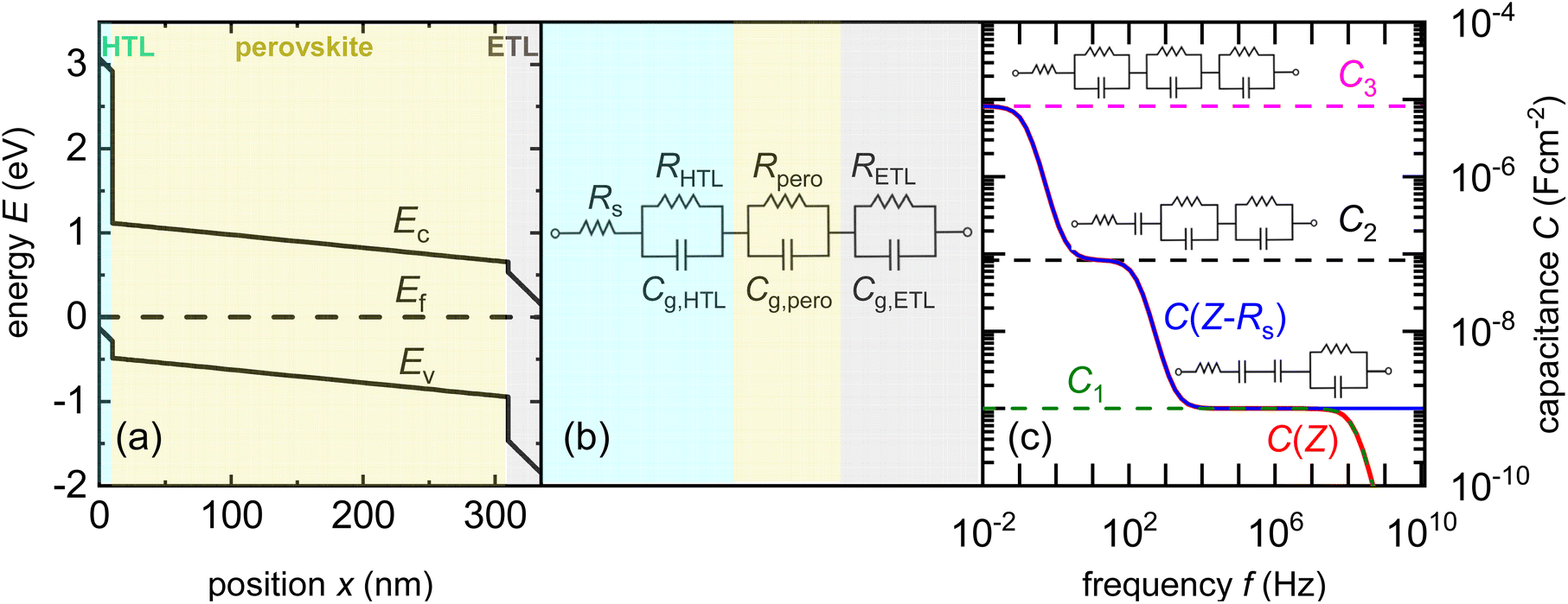 | ||
| Fig. 7 (a) Band diagram of a perovskite solar cell with the hole transport layer (HTL) and electron transport layer (ETL) highlighted. (b) AC equivalent circuit of the layer stack in (a), whereby each of the resistances except Rs must be understood as being inherently voltage dependent. (c) Frequency-dependent capacitance based on the equivalent circuit shown in (b), whereby each plateau shown corresponds to one of the resistances in the equivalent circuit being negligible relative to the value of 1/(jωC) of the respective R‖C element. Figure reproduced from ref. 88 under the terms of the CC-BY 4.0 license. © 2022. The authors of ref. 88. | ||
3.3. Pump-push photocurrent
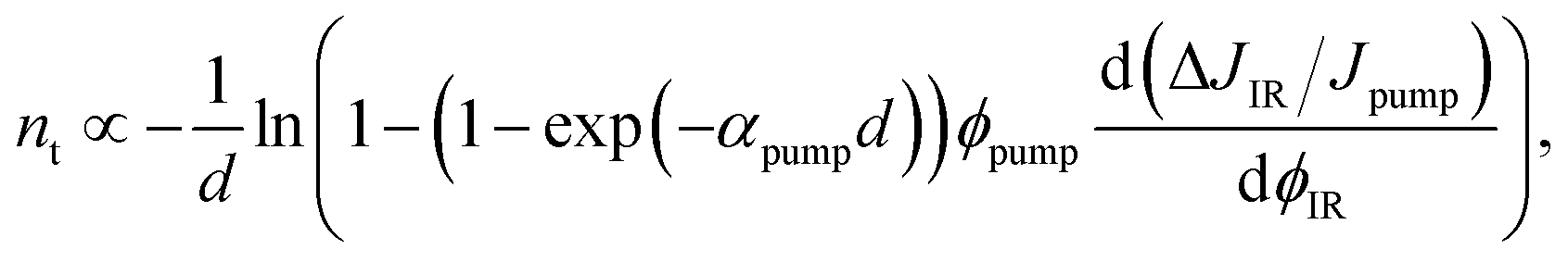 | (13) |
 | (14) |
 | ||
| Fig. 8 (a) Schematic of the pump-push photocurrent setup that involves a perovskite sample with contacts, a pump pulse creating electrons and holes, an IR push pulse to detrap trapped electrons or holes and an electrical detection system (lock-in amplifier) to measure the current flow. (b) Measurement of the additional current due to the IR push pulse as a function of excitation conditions showing that only if the pump pulse and the push pulse are on simultaneously, an excess current ΔJIR is flowing. (c) Schematic of the effect of pump and push pulse on charge carrier generation and charge detrapping. (d) Trapped carrier density as a function of time for samples with (“surface passivated”) and without (“pristine”) OAI passivation layer between absorber and Spiro-OMeTAD hole transport layer. Reproduced from ref. 93 under the terms of the CC-BY 4.0 license. © The authors of ref. 93 (2023). | ||
Fig. 8d shows an example of the application of eqn (14) to two different samples, whereby one (“pristine”) featured no passivation between the absorber and the hole transport layer (Spiro-OMeTAD) and the other sample (“surface passivated”) had an n-octylammonium iodide (OAI) passivation layer between absorber and HTL. We note the relative magnitude of the signals is considerably different as the data from the surface passivated sample is multiplied by 8 and therefore in absolute numbers much lower than that of the unpassivated sample. Thus, we can conclude that a significant effect of the trapping will come from the surface. A second observation is the time dependence of the initial rise of the signal, which may be due to different energetic or spatial distributions of trap states. For instance, it may take more time to fill surface states than bulk states as the filling of surface states would initially require diffusion of free electrons or holes to the surface.
4. Charge-carrier lifetimes and recombination coefficients
Recombination is a crucial loss process for solar cells because it reduces the flux of collected charge carriers, which leads to photocurrent but also reduces the energy per extracted electron, that is, the photovoltage. A typical method of quantifying recombination is to use a charge-carrier lifetime, as discussed in Section 2.4, or a recombination coefficient. Recombination coefficients are typically used for higher-order recombination mechanisms, such as radiative recombination, Auger recombination, or sometimes Shockley–Read–Hall recombination via shallow traps. Furthermore, recombination can be studied in semiconductor films, layer stacks, and complete devices (see Fig. 9). The key issue here is that interface recombination is often a rather important factor in understanding recombination in a device.60,94–96 Therefore, studying recombination on a film alone could be considered only moderately useful for understanding the final device. However, the more complex the sample structure is, the more complex the interpretation of the measurement methods will become.33 This is schematically shown in Fig. 9 which shows a range of different sample structures that could be analysed using optical methods that do not require contacts. The complexity of data analysis increases from left to right. In this chapter, we use the same approach, start with the least complex situation (films), and work our way up to the most complex (complete solar cells). | ||
| Fig. 9 Upper row: layer stacks from films on a glass substrate via films with transport and contact layers, such as ITO, towards complete cells. Bottom row: schematic band diagrams showing the processes that affect transient photoluminescence measurements. Figure reproduced from ref. 33 under the terms of the CC-BY 4.0 license. © The authors of ref. 33 (2021). | ||
4.1. Films
The key metric used for steady-state PL is the luminescence quantum efficiency Qlume, while the key metric for transient PL is the lifetime τ of the decay. There is no general or simple relationship between the two quantities. The luminescence quantum efficiency is given as the ratio of the radiative to total recombination rates while considering the efficiency pe = 1 − pr of light outcoupling, where pr is the probability of reabsorption. When neglecting Auger recombination, we then obtain
 | (15) |
![[thin space (1/6-em)]](https://www.rsc.org/images/entities/char_2009.gif) exp(−(EC − ET)/kT), p1 = NVexp((EV − ET)/kT), τn = (βnNT)−1, τp = (βpNT)−1. Furthermore, n0 and p0 are the equilibrium electron and hole concentrations, βn and βp are the capture coefficients of electrons and holes, EC is the conduction band edge, EV is the valence band edge, ET is the trap energy, NC and NV the effective density of states in the conduction and valence band, and NT is the trap density. In the simple case, where the defect is deep, and the semiconductor is intrinsic, eqn (15) simplifies to
exp(−(EC − ET)/kT), p1 = NVexp((EV − ET)/kT), τn = (βnNT)−1, τp = (βpNT)−1. Furthermore, n0 and p0 are the equilibrium electron and hole concentrations, βn and βp are the capture coefficients of electrons and holes, EC is the conduction band edge, EV is the valence band edge, ET is the trap energy, NC and NV the effective density of states in the conduction and valence band, and NT is the trap density. In the simple case, where the defect is deep, and the semiconductor is intrinsic, eqn (15) simplifies to | (16) |
In the logic of eqn (16) (deep defect and n = p), we can also determine an effective lifetime τeff that encompasses both recombination mechanisms (radiative and SRH) as
 | (17) |
An alternative quantification of recombination is possible using an effective recombination coefficient that includes both radiative and nonradiative processes. In the logic of eqn (16), the effective recombination coefficient is simply the denominator of the luminescence quantum efficiency, that is,
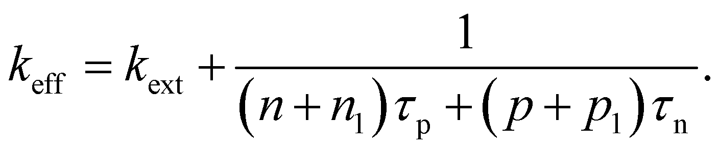 | (18) |
It is clear from the equations above that it is not, in general, possible to determine τeff from the luminescence quantum efficiency, except if the relation between n and p is known. For n = p for instance, we would obtain
| τeff = (kextn((Qlume)−1 − 1))−1. | (19) |
Thus, if kext and n can be determined separately, the lifetime can be directly determined from the luminescence quantum efficiency under these simplifying assumptions. Thus, the lifetime can only be deduced from steady-state experiments making strong assumptions.
In the case of transient photoluminescence, we observe the opposite situation. Now, the decay time can be deduced from the experimental data quite directly, while the comparison with, for example, a steady-state luminescence quantum efficiency, is much less straightforward. Again, we face the problem of making assumptions regarding the relation between n and p. If we assume the sample to be intrinsic as well as the absence of asymmetric trapping of one type of charge carrier (photodoping), the differential equation governing the decay would be given by
 | (20) |
A sensible definition of a decay time would be given by36
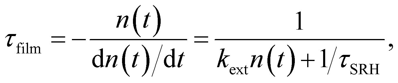 | (21) |
Note that there is no need to work out the solution for n(t) from eqn (20) to determine the decay time τfilm. The implicit solution of eqn (20), which gives the decay time, can be determined without knowing n(t). Eqn (21) is notably identical to eqn (17); that is, in the case of a deep defect and n = p, there is no difference in the information obtained from the steady-state or transient data.
Any steady-state or transient data on one of the three figures of merit should consider the carrier density or Fermi-level splitting. This is because all the equations discussed thus far show different regimes, that is, a constant decay time (or effective lifetime) for low carrier densities and a 1/n dependence for high carrier densities. Fig. 10 illustrates the effects of nonlinear recombination on the PL decay shape. The solid lines represent the calculated PL decays with different SRH lifetimes and the same fluence, that is, the same initial carrier density, n(t = 0). The dashed line has the same material parameters (kext, τeff) as the 2 μs SRH lifetime curve (blue). However, the fluence is lower. Hence, the decay appears different, and it is not immediately obvious that the two curves (blue and black dashed lines) originate from a sample with the same properties. However, if we plot the decay time according to eqn (21), the blue and black dashed curves lie perfectly above each other. The difference between the two is within this range. The black dashed curve starts at lower Fermi level splitting. Thus, plotting the decay time vs. Fermi level splitting allows us to create a representation of the data that is independent of fluence.
 | ||
| Fig. 10 (a) Calculated transient photoluminescence decays at the same fluence (solid lines), assuming different SRH lifetimes (100 ns, 500 ns, and 2 μs). The spheres represent the same material parameters as the solid blue line but with a lower laser fluence. (b) Decay time vs. Fermi level splitting derived from the data in (a). Notably, the blue solid line and the spheres overlap, indicating that the plot of decay time versus Fermi-level splitting is unaffected by the assumed laser fluence in this simple example. Therefore, the effects of laser fluence are usually a signature of effects such as diffusion or trapping. | ||
 | ||
| Fig. 11 (a) Double-logarithmic representation of the tr-PL decay of a triple-cation perovskite film (blue symbols) shows that the decay follows a power law from approximately 5 μs onwards. The green dotted lines indicate the shape of the exponential decays, and the red dashed line indicates the shape of the power law with a slope of −2. (b)–(d) Same data shown with a linear time axis. In these depictions, it is not clear whether the decay is a power law or multi-exponential decay. (e) Decay time vs. Fermi-level splitting data derived from the tr-PL decay shown in (a)–(d) (blue symbols). The lines show simulations assuming shallow defects plus one deep defect with a lifetime, as indicated in the legend. The parameters of the fit can be found in the ESI of ref. 22. | ||
The second obvious question triggered by power-law decays is what the meaning of the decay time is in the presence of higher-order recombination. The decay time continuously increases with time and thereby with decreasing Fermi-level splitting. In the example shown in Fig. 11, the decay time varies from tens of ns to >100 μs. As the PL quantum yield is approximately 2%, the origin of the power-law decay cannot be simply radiative recombination.22 It must be a non-radiative recombination mechanism that is quadratic in charge carrier density. A possible explanation is shallow defects that have the same recombination dynamics as radiative recombination without being radiative in nature.22
 | ||
| Fig. 12 (a) Photoluminescence transients of different lead-halide perovskite films on glass with the stoichiometry as indicated in the figure. For reference, a power law of type ϕ ∝ t−2 is shown. (b) Differential decay time τdiffversus Fermi-level splitting ΔEF and (c) versus time t. (d) Bimolecular recombination coefficient kdiffversus ΔEF for the same samples. Figure reproduced from ref. 25 under the terms of the CC-BY 4.0 license. © The authors of ref. 25 (2025). | ||
In addition to the conceptional aspects of analysing film data properly, there are also experimental considerations that become important especially in the context of the next chapters on comparison between film data and layer stacks. Here, the implicit or explicit assumption of many papers is that the addition of transport layers typically reduces the luminescence and the decay time relative to the surfaces to the glass substrate on one side and the N2 atmosphere of a sample holder on the other side. However, this assumption may not necessarily be true and thus, strategies have been developed to create better reference samples by passivating the two interfaces. Notable molecular passivation layers are 1,6-hexylenediphosphonic acid (HDPA)97 at the perovskite/glass interface and (3-aminopropyl)trimethoxysilane (APTMS)59,98 or n-trioctylphosphine oxide (TOPO).94,99
4.2. Layer stacks
Unfortunately, the problem seems to be difficult to treat analytically.33,34 The reason for this is shown in Fig. 13. After photoexcitation of the electron–hole pairs in the absorber layer of our layer stack, a current flows to equilibrate the quasi-Fermi levels. As initially, the layers that are not absorbing the light well (e.g. contact or transport layers) do not contain excess carriers, there will be charge transfer from the absorber to those layers. Fig. 13 shows a relevant case for halide perovskites, where both the perovskite and the electron transport layer (ETL) are intrinsic. In this situation, charge transfer to the ETL leads to the accumulation of electrons inside the ETL and the build-up of space charge. This space charge counteracts further charge transfer but also accelerates recombination by attracting holes in the perovskite to the interface. The space-charge effect seen in Fig. 13b depends on the laser fluence (how many charge carriers are there to begin with?) and the interfacial recombination rate (how long do they live?).
 | ||
| Fig. 13 Schematic of (a) charge transfer after photogeneration of charge carriers in the perovskite bulk, followed by (b) charge accumulation and recombination. Note that if recombination is sufficiently slow, electrons in the transport layer will have a sufficient density to accumulate close to the interface and attract holes to the other side of the interface, thereby accelerating recombination relative to the situation where space-charge effects are negligible. Modified after ref. 34. © The Royal Society of Chemistry (2018). | ||
The interfacial recombination rate depends on the recombination velocity, S, and the band offset. Fig. 14 illustrates how the lifetime depends on the Fermi level splitting for the case of a bilayer, as shown in Fig. 13 as a function of the band offset Δχ, defined as the difference in electron affinity between the absorber and the ETL. We note that the higher the band offset, the lower is the decay time in an intermediate range of injection conditions. At long times and low Fermi-level splittings, the effect of the offset disappears. Unfortunately, the physics contained in Fig. 13 and 14 could not be simulated using rate equation models that (only) consider charge transfer and recombination across the heterointerface. Instead, the Poisson equation (eqn (1)) must be solved to consider the Coulomb attraction between electrons and holes across the interface. The importance of the Poisson equation implies that a full drift-diffusion simulation is already the simplest conceivable type of simulation that would consider the relevant physics.34
 | ||
| Fig. 14 (a) Decay time derived from simulated tr-PL measurements of a perovskite-ETL bilayer as a function of band offset. The higher the offset at the interface (see (b)), the more pronounced the dip in the decay time at intermediate Fermi-level splittings (1.2 eV to 1.4 eV). Towards low Fermi-level splittings, the Coulomb attraction between electrons in the ETL and holes in the perovskites (see (b)) has become negligible and the effect of the offset disappears. Figure redrawn from ref. 33 under the terms of the CC-BY 4.0 license. © The authors of ref. 33 (2021). | ||
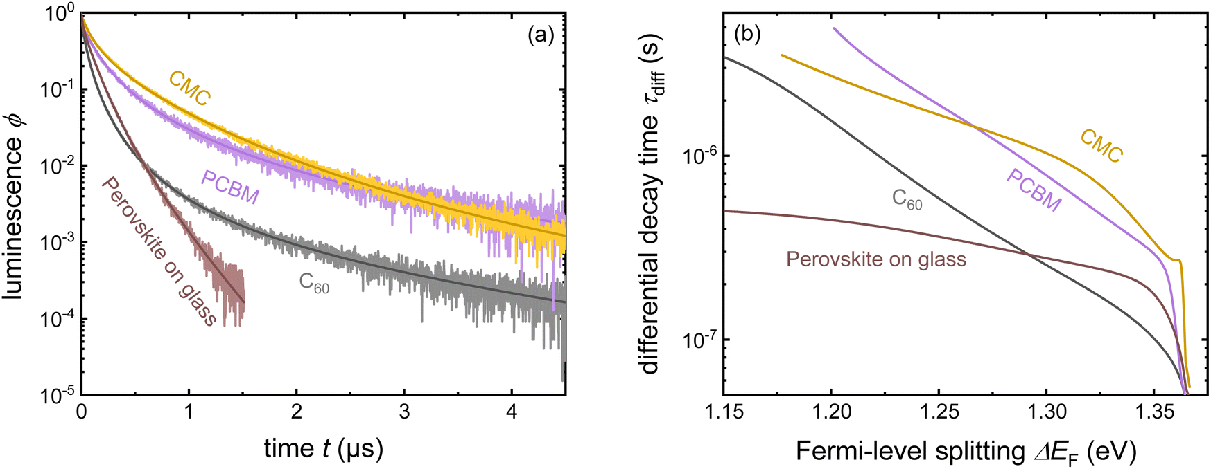 | ||
| Fig. 15 (a) Tr-PL measurements of three different samples with the layer stack Me-4PACz/triple-cation perovskite/ETL, where the ETL is PCBM, CMC, or C60. Furthermore, the tr-PL decay of the perovskite film on glass is presented as a reference. (b) Differential decay times were calculated from the fitted tr-PL data as a function of Fermi-level splitting. Figure reproduced from ref. 30 under the terms of the CC-BY 4.0 license. © The authors of ref. 30 (2023). | ||
Thus far, there are three types of models found in the literature. There are models that only consider one layer (the perovskite) and consider the ETL or HTL attached in one effective boundary condition.60,105–107 Here, the major disadvantage is that these models do not contain any band offset, so they would not be able to capture any of the physics contained in Fig. 14. Rate equation models108,109 could consider the ETL or HTL explicitly but would fail to account for Coulomb interactions. Finally, drift-diffusion simulations34,61,110 would account for all effects, but they are more time-consuming than the other two approaches and require learning a software tool (for instance from among the list found in Table 2).
Thus, future work will likely have to use time-dependent drift-diffusion simulations for data analysis, which is unfortunately the most complicated approach of the ones mentioned above. The challenge will then be to infer parameters from the decays. The decay depends on the energy level alignment as well as on the interface recombination dynamics and it is not entirely obvious how to disentangle the effects of both.61 In situations like that, Bayesian inference approaches such as the ones presented in ref. 40, 111 and 112 are likely to become highly useful. Bayesian inference means to fit simulations to experimental data and while doing so record the likelihood of material parameters (recombination velocity, band offset, etc…) being consistent with the experimental data. Bayesian inference thereby allows not only to identify the most likely material parameters explaining a certain experiment but also allows quantifying the confidence in the result and the need to add additional experimental data to improve the confidence.41
4.3. Devices
4.3.1.1 Introduction. Eventually, the spectroscopic results that are experimentally obtained on films or layer stack only matter if they have a predictive power on the performance of devices. In addition to e.g. correlating spectroscopic results on films with the performance of devices (see e.g. Fig. 14 in ref. 113) it is therefore logical to also extend the same forms of spectroscopy used on films to the complete devices. While the existence of metal contacts is a necessary condition for spectroscopy that involves electrical detection of signals (e.g. impedance, transient photovoltage), it is at least not an unsurmountable obstacle for purely optical spectroscopy such as transient or steady state photoluminescence.33 While steady-state PL going from films to complete devices was adapted quite early on and is reasonably straightforward as a method (see e.g. ref. 95 and 114), applying transient methods to devices adds an additional component, namely capacitive charging and discharging currents (J = C dV/dt) related to the capacitance C of the electrodes and the changes in external voltage V.
4.3.1.2 Challenge. In the case of devices, the complexity of all attempts to determine charge-carrier lifetimes is increased by the existence of the geometrical capacitance of the electrodes, which leads to various RC time constants that are not recombination lifetimes but may affect transient or frequency-domain measurements. It is often possible to distinguish between different types of time constants based on their dependence on the voltage or light intensity. Thus, the frequently observed habit in the literature on halide perovskites to show only one decay of transient photovoltage or only one arc of a Nyquist plot in impedance is unhelpful because it makes it impossible to attribute these time constants to different physical phenomena. Fig. 16 provides an example of a simulated tr-PL decay of a perovskite solar cell, where the electrode capacitance of the device was varied in the simulation.33 This leads to different decays at longer times that lead to a continuously rising differential decay time towards lower Fermi-level splittings. This behaviour is caused by the RC time constant of the electrode capacitance discharging via the recombination resistance of the solar cell, which can lead to extremely long decay times if the voltage is sufficiently low and the recombination resistance therefore sufficiently large.
 | ||
| Fig. 16 (a) Simulated transient PL decays as a function of time for three different values of the device capacitance. Differential decay times resulting from the three decays showing the effect of the capacitance, which makes the decay times become longer towards lower values of the Fermi-level splitting. Redrawn after ref. 33 under the terms of the CC-BY 4.0 license. © The authors of ref. 33 (2021). | ||
4.3.1.3 Opportunity. All small-signal transient and frequency-domain measurements of halide perovskites contain at least two features that can be analysed. For instance, in the case of transient photovoltage measurements, the rise and decay are visible in each transient. Traditionally, only the decay has been analysed, but the rise also contains information. Furthermore, the two time constants that can be determined at each light intensity and voltage can be compared with the voltage dependence of the different physical phenomena that can occur within a perovskite solar cell. These phenomena include different types of recombination, extraction, and discharge of the electrodes by reinjecting charge carriers through the charge-transport layers back into the absorber where they can recombine.
A possible mathematical approach to compare experimental data with a model is to create a linearised model of two coupled differential equations describing the time dependence of the external voltage, as well as quasi-Fermi level splitting. This is a sensible approach, as the quasi-Fermi level splitting inside the perovskite absorber layer at open circuit should be reasonably constant in good devices. Such a model with two linear differential equations can be written as a matrix equation, where the time constants are given by the negative inverse eigenvalues of the matrix.17 The major advantage of 2 × 2 matrices is that their eigenvalues are typically simple enough to connect them with a physical meaning. In the following, we describe the results for the case of transient photovoltage measured using a bias light that keeps the solar cell at open circuit. The cell is then perturbed by illumination with a pulsed laser, which creates a small additional open-circuit voltage. The ΔVoc first increases and then decreases again such that before the pulse and at long times after the pulse, the ΔVoc is zero and the open-circuit voltage is entirely given by the bias light intensity. There are two well-distinguishable time constants, one for the rise and one for the decay of the ΔVoc. The eigenvalues can be determined analytically and further Taylor-expanded to simplify the equations. The rise time then follows as17
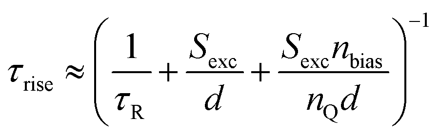 | (22) |
 | (23) |
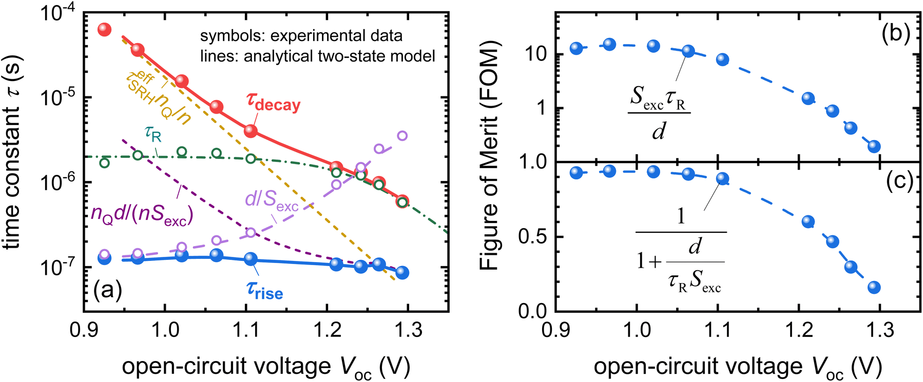 | ||
| Fig. 17 (a) Time constants extracted from the TPV rise and decay compared with the different terms in eqn (22) and (23) which are shown as dashed or dash-dotted lines. (b) and (c) Figures of merit that follow from the analysis of the rise and decay times shown in panel (a). Reproduced from ref. 17 under the terms of the CC-BY 4.0 license. © The authors of ref. 17 (2023). | ||
The advantage of an analysis that considers both the time constants is that information on both recombination and extraction can be obtained from the data. The likelihood of extracting charge carriers depends critically on the dimensionless ratio
 | (24) |
The efficiency of collecting charge carriers then follows from the ratio via
 | (25) |
Fig. 17b and c show the two figures of merit as a function of Voc, as determined from the data shown in Fig. 17a. The main advantage of the method presented above for an example of transient photovoltage is that a variant of this approach applies to all small-signal methods applied to full devices. Similar approaches have already been published for methods such as impedance, as well as intensity-modulated photocurrent and photovoltage spectroscopy (IMPS and IMVS).27
4.3.2.1 Introduction. In addition to time-domain methods, there are also small-signal frequency domain methods that can be applied to perovskite solar cells. The approach is usually to set a bias (DC) voltage and light intensity, then measure the AC response of the solar cell to some periodic excitation (e.g. a periodic voltage signal) and then study the behaviour of real and imaginary part of the transfer function (output/input) as a function of the different variables of the measurement which include primarily frequency, temperature and DC bias conditions. There are several conceivable types of excitation signals and therefore transfer functions. The most popular variants are impedance (Z = Ṽ(ω)/
![[J with combining tilde]](https://www.rsc.org/images/entities/i_char_004a_0303.gif) (ω)), where the ratio of complex voltage to complex current is studied, as well as intensity modulated photocurrent (IMPS) and photovoltage (IMVS) spectroscopy.115–117 Here, the excitation is a modulated light intensity, and the measured signal is either the photocurrent or photovoltage induced by the modulated light intensity
(ω)), where the ratio of complex voltage to complex current is studied, as well as intensity modulated photocurrent (IMPS) and photovoltage (IMVS) spectroscopy.115–117 Here, the excitation is a modulated light intensity, and the measured signal is either the photocurrent or photovoltage induced by the modulated light intensity ![[small phi, Greek, tilde]](https://www.rsc.org/images/entities/i_char_e0e2.gif) (ω). The transfer functions are therefore Q = (ω)/q(ω) for IMPS and W = Ṽ(ω)/q(ω) for IMVS. Given these definitions, we note that the impedance should be the ratio of the transfer functions of IMVS and IMPS, i.e. Z = W/Q.118 This implies that two out of the three measurements should contain all information that could be obtained by measuring all three.
(ω). The transfer functions are therefore Q = (ω)/q(ω) for IMPS and W = Ṽ(ω)/q(ω) for IMVS. Given these definitions, we note that the impedance should be the ratio of the transfer functions of IMVS and IMPS, i.e. Z = W/Q.118 This implies that two out of the three measurements should contain all information that could be obtained by measuring all three.
4.3.2.2 Challenge. The purpose of the measurements is to determine time constants that allow the researchers to quantify recombination, extraction or other physical processes happening inside the solar cell in a similar manner as explained for the example of TPV in Chapter 4.3.1.115,117,119,120 As was the case for TPV, the obvious challenge of this approach is not so much to actually determine the time constants but to assign meaning to these constants in such a way that a high confidence in the result is obtained. This is hampered by the frequent inability to distinguish between different processes without having additional information. There are essentially four competing approaches to analyse the data and extract meaningful information, namely equivalent circuits,117 diffusion recombination models,121 matrix models27,28 and full drift-diffusion simulations.27 The most traditional approach is to use equivalent circuit models that enable fitting the real vs. imaginary part of the transfer function as a function of frequency. The simplest conceivable equivalent circuit model would be a resistor R and capacitor C connected in parallel leading to an impedance
 | (26) |
This impedance Z leads to a semicircular Nyquist plot (see Fig. 18a), where real and the (negative) imaginary part of the impedance Z are plotted vs. each other as a function of angular frequency ω. The maximum of the imaginary part is reached exactly if ω = (RC)−1 and the RC product is then typically extracted as a time constant as shown in Fig. 18b.
 | ||
| Fig. 18 (a) Nyquist plot of an ideal parallel connection between a resistance R and a capacitance C for a constant capacitance of 100 nF cm−2 and three resistances. The higher the resistance, the larger the semicircle. The peak of the semicircle is reached at the maximum of the negative imaginary part (−Z′′) of the impedance. The higher x-axis intersect of the Nyquist plot corresponds in this simple case exactly to the value of R. (b) Plot of −Z′′ as a function of the angular frequency ω showing that the peak of −Z′′ always corresponds to 1/RC. | ||
To interpret the time constant, we need to consider the different contributions to the capacitance and resistance of a solar cell as a function of bias conditions. In many situations, the RC time constant may indeed correlate with recombination and the open-circuit voltage which may have been partly responsible for the popularity of the method also in technology-oriented publications. Let us briefly assume the resistance of the solar cell is indeed dominated by the recombination current flowing in the dark or under illumination. The recombination current density has the typical form J = J0exp(qV/nidkT), where J0 is the saturation current density and nid is the ideality factor. Then, the differential resistance at a bias voltage V is
 | (27) |
If two solar cells are primarily different in their recombination rate at a given carrier density, then they would have different values of the saturation current density J0 which contains all information on recombination except for the influence of voltage on carrier density. Thus, any variation of e.g. passivation quality would impact J0, thereby Voc = (nidkT/q)ln(Jsc/J0 + 1) and in consequence also the RC time constant if measured at a constant voltage. Note that measuring the samples at their respective open-circuit voltages would lead to a completely different trend. In this case, we would obtain
 | (28) |
As outlined in ref. 27, 88 and 119, even if R is dominated by recombination, the RC time constant may not necessarily be the same thing as a recombination lifetime. In many situations, the value of C is influenced or dominated by the capacitance of electrodes or transport layers rather than being the chemical capacitance of the absorber layer. In these situations, the RC time constant may still correlate with Voc (because of R) but being often much longer than the actual lifetime measured by e.g. photoluminescence measurements.36 This situation is completely analogous to the case previously discussed for transient photovoltage. In Chapter 4.3.1 we discussed that the decay time of a TPV measurement is approximately
 | (29) |
| τ ≈ RrecCg + RrecCμ. | (30) |
4.3.2.3 Opportunity. In essence, the strategy to make sense of frequency domain measurements is identical to the strategy for small signal transient measurements such as TPV.27,28,119,120 In isolation, i.e. measured at one bias condition, the time constants are largely meaningless as they do not allow the researcher to identify their origin. While being meaningless in absolute terms, they might still correlate with e.g. Voc as they might contain the recombination resistance. This may again lead to a confirmation bias of the type that the result correlates with my expectation so my interpretation of the data must be correct and likely meaningful. This can be completely wrong and further be a rather useless bit of additional evidence. Imagine the situation that you already know a trend in parameter A. If you now measure a parameter B that correlates with parameter A (say via a linear function), then knowing B does not help me except for confirming their correlation. Thus, the whole value of measuring a single Nyquist plot of a solar cell might provide negligible additional information if I want to understand a given trend in e.g. Voc. To infer meaning from frequency-domain measurements on perovskite solar cells, it is therefore necessary to measure over a range of bias conditions (voltages or light intensities) and then to apply a model that contains the parameters of interest. The level of complexity of the model depends on the situation. In many situations, an analytical approach via the eigenvalues of matrices as proposed in ref. 27 and 28 may be sufficiently complex to assign meaning to the data. Complementary measurements that are sensitive to recombination but for instance not to other terms in the equation such as the geometric capacitance are then useful to increase the confidence in the interpretation of the data. Such additional measurements could then be for instance tr-PL measurements on films or layer stacks that do not have a second electrode.
5. Charge transfer and extraction
5.1. Voltage dependent photoluminescence
If charge transfer and transport are supposed to be measured on a complete solar cell, it is often useful to study the photoluminescence of the solar cell and measure it as a function of the external voltage.124,126,127,130 The photoluminescence is proportional to the product of electron and hole densities in the perovskite absorber and thereby to exp(ΔEF/kT). This implies that the Fermi-level splitting ΔEF can be obtained from a suitably calibrated measurement of the voltage-dependent PL. As the overall recombination current scales with Fermi level splitting, it is possible to quantify the voltage-dependent recombination current from the PL(V) measurements.127 While these data do not directly quantify the transport through the ETL and HTL, they do quantify recombination losses that are due to insufficiently fast charge collection. As the speed of charge collection is often limited by transport through CTLs, the result shown in Fig. 19 is a viable strategy for quantifying the effect of insufficiently conductive CTLs. Whenever trends as a function of the type or processing of ETL or HTL become visible (as seen in Fig. 17 for the case of a variation of ETL type), the influence of the CTLs on slowing down charge extraction and increasing recombination can be quantified. This approach is useful in halide perovskites, as the fill factors might be reasonably good, although there are still significant charge collection losses. This is due to ion-induced screening of the electric field, which leads to voltage-independent collection losses that hardly appear in the fill factor.127
 | ||
| Fig. 19 Example of the application of the voltage-dependent PL method to quantify charge collection losses. (a) Fermi-level splitting versus external voltage obtained from the voltage-dependent PL. Data were obtained for three solar cells that differed in the ETL used: C60, PCBM, or CMC. (b) The recombination current density as a function of the external voltage was calculated from the PL(V). Figure reproduced from ref. 30 under the terms of the CC-BY 4.0 license. © The authors of ref. 30 (2023). | ||
5.2. Transient and steady-state surface photovoltage
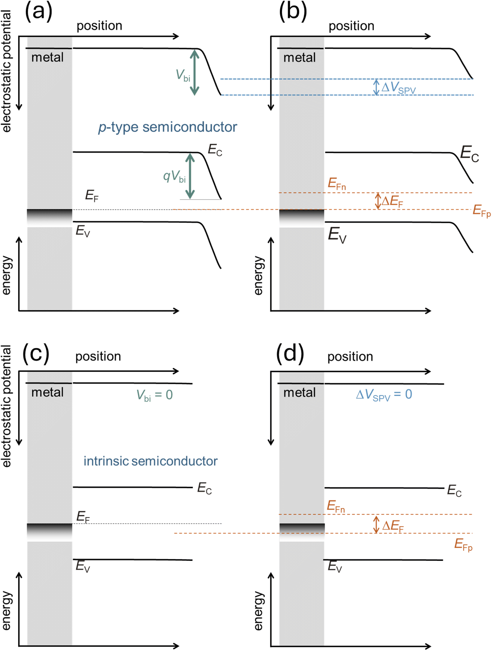 | ||
| Fig. 20 Schematic to explain the difference between surface photovoltage ΔVSPVvs. Fermi level splitting ΔEF in doped (a and b) and undoped semiconductors (c and d). In the case of a p-type semiconductor forming an ohmic contact to a metal substrate, there is an electrostatic potential difference Vbi in equilibrium (a). Under non-equilibrium, low level injection conditions, the semiconductor will show a Fermi level splitting ΔEF and an electrostatic potential difference Vbi − V, where qV = ΔEF. Thus, a PL measurement to determine ΔEF, would provide the same information as the surface photovoltage. In case of an intrinsic semiconductor with blocking contacts (c) Vbi = 0, and any illumination would still lead to zero electrostatic potential difference (d) as there is no symmetry breaking element in the system. Thus, in this case one could measure a PL but the SPV would be zero. Thus, the comparison of PL and SPV can be sensitive to the existence (or absence) of symmetry breaking elements that support charge separation. | ||
 | ||
| Fig. 21 Transient SPV measurement of an ITO/SAM/perovskite sample, whereby the different features are tentatively explained using schematics of the phenomena that likely contribute to the observations. These are from short times to long times, the trapping of electrons at the ITO/SAM interface, the hole transfer to the ITO, the released of trapped electrons from the ITO/SAM interface and the recombination of detrapped charge carriers that are reinjected into the perovskite absorber. Figure reproduced from ref. 132 under the terms of the CC-BY 4.0 license. © The authors of ref. 132 (2021). | ||
 | ||
| Fig. 22 (a) Transient SPV and (b) transient photoluminescence measurement of an ITO/SAM/perovskite/C60 sample with different interlayers (piperazinium iodide, PI, and LiF) between perovskite and C60. In this study, the PI led to a sharp rise and large amplitude of the SPV signal (suggesting fast charge separation) and to slow recombination at the same time (seen in the tr-PL). This is consistent with the improved solar cell performance (see ref. 16). Figure reproduced with permission from ref. 16. © The authors of ref. 16 (2023), some rights reserved; exclusive licensee American Association for the Advancement of Science. | ||
Meta-studies on mobilities in halide perovskites have previously found that the mobilities show a particularly strong method-specific variation133 as well as a strong variation between thin films and single crystals.134 An important reason for these variations is the sensitivity of different methods to the presence and orientation of grain boundaries. Let us assume that the grain sizes are on the order of typical thin film thicknesses (hundreds of nanometres), then grain boundaries are much more likely to affect in-plane transport as opposed to out-of-plane transport. Fig. 23 illustrates the different techniques discussed in Chapter 6 and the type of transport they are sensitive to or depending on (in the case of the JV curve). The spectrally resolved transient PL (Fig. 23a) measures the depth dependence of the carrier concentration profile, which homogenises as a function of time by diffusion. Homogenisation leads to larger self-absorption losses, which cause a redshift in the spectrum. Thus, this method measures out-of-plane mobilities that are particularly relevant for normal device operation (see Fig. 23d). The optical pump terahertz probe (OPTP) measures the change in THz probe transmission as a function of the time delay to an optical pump. The high frequency of THz radiation ensures that the mobility is measured on a length scale of nanometres, that is, within a single grain. Thus, OPTP often gives the highest values of mobility.133,134
 | ||
| Fig. 23 Schematic illustration of different measurement methods in the context of charge carrier mobilities applied to polycrystalline materials (inspired by Fig. 5c in ref. 135). The active layer is illustrated by transparent cubes, indicating the existence of grain boundaries that are primarily parallel to the surface normal of the film. This leads to different effects of the grain boundaries on the determined mobility or performance of the solar cell. (a) Transient and spectrally resolved PL, where the diffusion of charge carriers into the depth of the film after photoexcitation leads to a red-shift of the PL spectrum as a function of time and allows determination of the out-of-plane mobility which is relatively unaffected by the grain boundaries. (b) OPTP measurement that probes the intragrain motion of photogenerated charge carriers via the relative transmission change of a THz probe pulse. (c) Transient microwave photoconductivity measures the intra- or inter-grain motion of charge carriers via changes in the microwave reflectance. (d) Solar cell JV curves primarily require vertical (out-of-plane) transport within the active layer and lateral transport within the contacts (primarily the TCO) to achieve good performance. (e) The photo-Hall effect allows access to the transport properties of electrons and holes separately by measuring the Hall voltage VH for a given applied voltage and magnetic field as a function of steady-state illumination intensity. | ||
5.3. Vertical electrical measurements (out of plane)
In a solar cell, transport is mostly vertical through the absorber layer and lateral only within the highly conductive contact layers consisting of metals and transparent conductive oxides. Thus, the absorber mobility of interest is generally the out-of-plane mobility.While the approach discussed in ref. 32 and 138 requires somewhat costly equipment, the general idea is feasible with relatively minor alterations to a traditional time-correlated single photon counting setup as it is available in numerous laboratories working on halide perovskites. The setup discussed in ref. 32 and 138 used either a gated CCD camera to generate spectral resolution at every delay time, or they combined time-correlated single photon counting (TCSPC) detectors with wavelength-selective filters that allow detection of a different part of the PL spectrum. The latter method was implemented in ref. 32 using a beam splitter and two detectors (each with a different filter) measuring simultaneously. In principle, it could also be performed using a single detector and by measuring the sample, for example, first with one filter and then with another. This has the huge advantage of negligible additional costs for the setup relative to those available in many laboratories. However, it has a practical disadvantage that there is no built-in mechanism to detect any changes in the sample properties between the measurements. This could be overcome by several repeated measurements to check whether any difference in the decay dynamics is due to transport or changes in the sample properties.
Fig. 24 shows an example of the spectrally resolved tr-PL data measured at different fluences.144 The samples were triple-cation perovskites, similar to those used for Fig. 10. If we assume that the PL intensity ϕ ∝ np, we can then determine the geometric mean  of the charge carrier density as a function of time (see Fig. 24b). The data for the lower two fluences is offset in time such that the data fits to each other, except for a short initial part, where the carrier density decays rapidly to the its longer time trajectory. Fig. 24c shows the resulting differential decay time calculated using eqn (21). We note that the common trajectory shown in Fig. 19b leads to a common decay time where all three traces overlap. However, at the highest Fermi-level splitting for each of the three curves, the decay time was shorter than the predicted trajectory. This part of the decay time corresponds to the fast initial decay shown in Fig. 24b. Fig. 24d shows the condensed information resulting from the PL spectra, expressed as the ratio of the low-to high-energy parts of the PL spectra. At longer times and lower Fermi-level splitting, the carrier concentration becomes more homogeneous which increases the self-absorption effect and results in a redshift of the spectra. This redshift translates into an increase of the ratio R with time and decreasing Fermi-level splitting ΔEF. We note that the part of the data that shows a change in R is identical to the part of the decay time data in Fig. 24c, where each individual fluence diverges from the trajectory at longer times. Mathematically, we observe a transition from a partial to an ordinary differential equation governing the behaviour of tr-PL. At early times (highlighted in shades of green), the decay is governed by a combination of diffusion and recombination (or trapping) of charge carriers. Even in the complete absence of recombination, diffusion alone can lead to a reduction in the PL intensity as it moves carriers away from a region of high np to a situation where the electron and hole distributions are equally distributed throughout the depth. Even if
  does not change (no recombination or trapping), the term
  will change just by diffusion. As long as
  changes differently than
  , the spatial distribution of n(x) will matter and one would have to solve a partial differential equation for the variable n(x, t) to simulate the decay. Once diffusion leads to a homogeneous carrier distribution (n(x) = const), the depth dimension ceases to matter, and the mathematical problem reduces to the solution of an ordinary differential equation in time. The solution of the ordinary differential equation will then depend only on n (and p) and not separately on time t. Thus, measurements at different fluences will end up following the same trajectory at any given carrier density n (or Fermi-level splitting ΔEF). From the change in the ratio R with time, mobility can be inferred by fitting a diffusion-recombination model to the data. This model requires precise knowledge of the optical properties of the perovskite film, which creates a challenge for data analysis. However, a major advantage of the model is that it allows the determination of both the decay time and the (relevant) out-of-plane mobility of a film using contactless measurements.
 | ||
| Fig. 24 (a) Photoluminescence decays taken at different fluences on a double-logarithmic plot. (b) Same decays but now with the carrier concentration on the y-axis and with the time axis shifted such that the data overlays. (c) Differential decay time vs. Fermi-level splitting. (d) Spectral shift ratio vs. Fermi-level splitting. The regions highlighted in green represent regions of the decay where diffusion matters, while the regions highlighted in blue represent the part of the decay where all curves follow a common trajectory. Data for the figure and further information on the sample is found in ref. 144. | ||
5.4. Lateral measurements (in-plane)
 | (31) |
 | (32) |
 | (33) |
Let us assume a semiconductor with deep acceptor-like traps (negatively charged when full and neutral when empty), such that p ≥ n, as shown in Fig. 25a. With increasing illumination, the photogenerated free electron Δn and hole densities Δp will start to exceed the trapped electron density and due to charge neutrality Δn and Δp will approach each other as seen in Fig. 25b. If we assume that μn = μp, the Hall mobility approaches zero towards high light intensities, as shown in the upper panel of Fig. 25d. At low light intensities, the Hall mobility is determined by the hole mobility and scattering coefficient r. In this case, also parasitic conductances (called σS in ref. 145) can affect the result. If we assume the electron mobility to largely exceed the hole mobility, we will see the opposite trend of Hall mobility with light intensity. Now, the low illumination result will be the same, but the high illumination result will be significantly higher and will yield a difference in electron and hole mobilities.
 | ||
| Fig. 25 (a) Charge carrier generation, recombination, and transport in p-type semiconductor with acceptor-like defects. (b) Simulated dependence of electron, hole, and trapped electron density as a function of illumination. (c) Schematic of the Hall effect measurement under illumination, where (1) represents the current source, (2) represents the electrical contacts, (3) represents the magnet, (4) represents the induced Hall voltage, and (5) represents the illumination. (d) Simulation of Hall mobility in p-type material with identical (upper panel) electron and hole mobilities and electron mobilities that are a factor of 10 higher than the hole mobilities (bottom panel). The symbol σS indicates the value of the parasitic conductivity that affects the correct determination of the Hall mobility. Figure reproduced from ref. 145 under the terms of the CC-BY 4.0 license. © The authors of ref. 145 (2024). | ||
Fig. 26 shows the results of the application of the photo-Hall method to a triple-cation, lead-halide perovskite thin-film sample (∼500 nm thickness), where each parameter is plotted versus the light intensity or photogeneration rate G. The sample had acceptor-like defects, such that holes were the majority carriers in the dark. The photoconductivity increases with the generation rate (see Fig. 26a) while the Hall coefficient RH decreases (see Fig. 26b). This is a logical consequence of the conductivity σ = q(pμp + nμn) depending on the sum of electron and hole conductivities, while the Hall coefficient contains a difference in hole and electron transport properties (RH ∝ pμp2 − nμn2). The Hall mobility μH (see Fig. 26c) increases slightly (probably owing to parasitic conductance) but then drops to near zero for the highest measured illumination intensities, implying that the hole and electron mobilities are approximately equal. An important feature of the photo-Hall method is that the electron and hole densities can be determined independently from the Hall coefficient, the photoconductivity, and the knowledge of the electron and hole mobilities that can be derived from the Hall mobility. The electron density results from
 | (34) |
 | (35) |
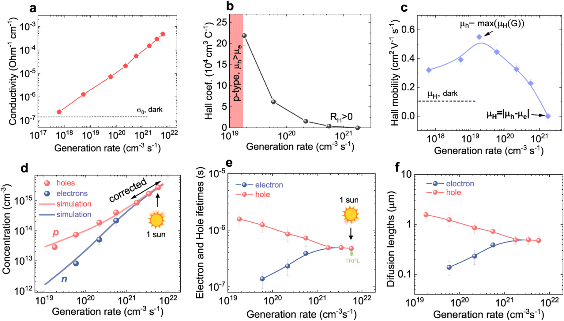 | ||
| Fig. 26 (a) Conductivity, (b) Hall coefficient, and (c) Hall mobility of a triple-cation lead-halide perovskite thin film measured as a function of light intensity and, thereby, generation rate. The decrease in the Hall coefficient RH indicates the increasing relevance of the minority-carrier term in the numerator of eqn (31). (d) Electron and hole concentrations as a function of the generation rate. (e) Electron and hole lifetimes as functions of the generation rate. (f) Diffusion lengths of electrons and holes as a function of generation rate. Figure reproduced from ref. 145 under the terms of the CC-BY 4.0 license. © The authors of ref. 145 (2024). | ||
The charge carrier densities are plotted as a function of light intensity in Fig. 26d showing that they approximate each other at high light intensities, whereas the hole density exceeds the electron density at low light intensities. This suggests the existence of acceptor-like traps with a density that is sufficiently high to lead to a difference in electron and hole densities at low injection due to charge neutrality n + nt = p, where nt is the density of the trapped electrons. At higher light intensities, nt cannot further increase but is limited by the total trap density Nt, whereas n and p continuously increase until n ≈ p.
A further advantage of this method is that the knowledge of carrier densities allows one to derive information on charge-carrier lifetimes. The approach proposed in ref. 145 is to define an electron
 | (36) |
 | (37) |
In contrast to the notation used in ref. 145, I introduced the tilde (∼) to indicate that these definitions are different from the SRH lifetimes for electrons and holes that we used previously, e.g. in eqn (17), (20), and (21).
It is worth briefly comparing the definitions in eqn (36) and (37) with the SRH lifetimes used previously. The data suggest a trap that is not too shallow and not too high in density, as its effect disappears towards higher light intensities. Thus, for simplicity, we assume that G = RSRH, and that RSRH is limited by a deep defect. Then we can write
 | (38) |
Thus, at low light intensities, where p ≫ n, we obtain the simple result ![[small tau, Greek, tilde]](https://www.rsc.org/images/entities/i_char_e0e5.gif) n = τn while towards higher light intensities, we obtain a higher value n = τn + τp. This mathematical result corresponds well to the observed effect of n increasing with generation rate (see Fig. 26e) and then saturating to a constant value. The intuitive explanation for this trend is that for low light intensities, electrons are the minority carriers and, for every recombination event, the capture of electrons will be rate limiting, while the capture of holes will be fast in comparison. Towards higher light intensities, this is no longer true, and the capture of electrons and holes will be similarly fast, implying that both the electron and hole SRH lifetimes contribute to the measured (Hall) lifetime n. The hole lifetime instead is given by
n = τn while towards higher light intensities, we obtain a higher value n = τn + τp. This mathematical result corresponds well to the observed effect of n increasing with generation rate (see Fig. 26e) and then saturating to a constant value. The intuitive explanation for this trend is that for low light intensities, electrons are the minority carriers and, for every recombination event, the capture of electrons will be rate limiting, while the capture of holes will be fast in comparison. Towards higher light intensities, this is no longer true, and the capture of electrons and holes will be similarly fast, implying that both the electron and hole SRH lifetimes contribute to the measured (Hall) lifetime n. The hole lifetime instead is given by
 | (39) |
p as compared to n. For low generation rates, we have  and thus (given p ≫ n) a higher value as compared to higher generation rates, where n = p = τn + τp. Thus, the data show a consistent behaviour for a sample with acceptor-like traps of medium density and offer strategies to connect the quantities with tilde that are directly derived from observables to the quantities without a tilde that are parameters of a model (here the SRH model) and that could be used as input parameters, for example, in numerical device simulations. Fig. 26f finally shows the electron and hole diffusion lengths based on the definitions
  and
and  . Given the similarity in electron and hole mobilities determined using the photo-Hall measurement, these diffusion lengths show the same trends as the lifetimes discussed previously.
Thus, to summarize, the photo-Hall effect measurement provides a rather unique combination of information as it is sensitive to both transport and recombination as well as to electron and hole properties independently. The challenges in going forward will be associated with a better understanding of the effects of possible parasitic conductivities (e.g. ionic motion) and the translation of the parameters obtained from experiments (particularly lifetimes and diffusion lengths) to the parameters of the relevant models for recombination and transport. Furthermore, it is important to achieve a better understanding of the effects of surface passivation on effective Hall lifetimes.
5.5. Microscopic measurements
In a round-robin study on OPTP and TRMC,135 the authors initially looked at published data and noted significant variations in the mobility values from these two methods. Of course, these variations in the literature could be partly due to variations between samples. These differences nearly disappeared when a series of similar samples were measured using the same setup. However, some variation was maintained when comparing measurements of the same samples using setups from different groups. Interestingly, the authors identified the cause “human error” as the biggest effect, which suggests that despite the significant variation in the obtained mobility values, there is no inherent issue with the methods that makes them less reliable or less comparable.
TRMC has already been extensively used to study recombination as a method with information content comparable to that of transient photoluminescence. An opportunity that has so far rarely been used (exception is e.g. ref. 111) is the combination of methods that are sensitive to np (such as tr-PL) and n + p (such as TRMC or transient absorption spectroscopy). This should lead to additional insights into trapping, as this would lead to imbalances between electron and hole densities (due to charge neutrality). One of the rare examples of comparing tr-PL with transient absorption spectroscopy lead to the conclusion that the effect of charged defects under illumination on recombination and recombination dynamics must be substantial in the studied multi-cation films but insignificant in MAPI.44
6. Band diagrams and band offsets
6.1. Band offsets and alignment
This method poses a range of challenges whenever absolute numbers of these energy levels are required. First, UPS measures energy levels in ultrahigh vacuum (UHV) using a method that is very surface-sensitive (a few monolayers), which implies that it accesses the surface of a film, but not the actual interface of a device. Furthermore, contamination of the sample surface might have affected the results. Second, the determination of the valence band edge is an attempt to assign a number to a continuously changing function. Depending on the exact shape of the data, different evaluation techniques might lead to drastically different results. Fig. 27 illustrates this problem by showing the same data on logarithmic (red) or linear scales (blue) originating from three different variants of photoelectron spectroscopy applied to the same sample.31 These are the most commonly seen UPS with a He source (He-UPS), a UPS variant using a near-UV light source (NUPS),31 and a variant called constant final state yield spectroscopy (CFSYS),158 which offers a particularly high dynamic range. The numbers indicated in the figure are the distance from the Fermi level to the valence band edge (i.e. −1.19 eV means that the valence band is 1.19 eV below the Fermi level). We note that for the logarithmic method, we observe variations from EF − EV = 0.68 eV to 1.19 eV distance, while for the linear method the differences are smaller, but the absolute values are higher, suggesting a strong n-type doping of the surface of the film. This strong surface doping is likely an artefact of the linear extrapolation method, which overestimates the distance EF − EV. Thus, different photoelectron spectroscopy methods and different ways of assigning a number (the valence band edge) to a measured spectrum can lead to a range of energy levels of nearly 1 eV, which could be (depending on the band gap of the semiconductor under investigation) the difference between highly n-type or highly p-type. Thus, the interpretation of the data can invert the conclusion by 180° thereby leading to a massive challenge for any quantitative data interpretation. I will therefore come back to this point in the “opportunity” section of this chapter.
 | ||
| Fig. 27 Comparison of different fitting approaches for determining the valence band edge for triple-cation lead-halide perovskite films on glass/ITO substrates. The data are plotted as a function of the binding energy with the Fermi level of the ITO substrate, defining the zero of the energy scale. (a) Satellite-corrected He-UPS, (b) NUPS (using a UV source with 6.5 eV photon energy), and (c) CFSYS measurements. The assignment of the valence band edge was achieved in all cases by obtaining the intersection of a fit to the linear or logarithmic band edge data with the background. Especially in the case of the logarithmic method, the intercept critically depends on the dynamic range of the measurement, which sets the level of the background and, consequently, the position of the intercept. Note the large method-induced differences in the logarithmic determination of the valence band edge, as well as the generally much higher distance EF − EV obtained for the linear method. Reprinted with permission from ref. 31. © American Chemical Society (2021). | ||
In addition to the challenge of quantifying the band edge positions via photoelectron spectroscopy, there are also conceptional problems in how to interpret the band edges. If we had a device geometry consisting entirely of crystalline inorganic semiconductors, we could argue that the band edge is well defined as the onset of the square-root-like density of states that we expect to have in 3D crystals. In the case of halide perovskites, however, we often have interfaces between inorganic and organic materials, where the meaning of the offset becomes more difficult to define. Let us take for instance, the interface between an inorganic material with a square-root-like density of states and a molecular semiconductor with a Gaussian density of states, the concept of an offset will critically depend on the characteristic energy that we use for the Gaussian density of states. Here, the onset will be impossible to use as a Gaussian continually decreases towards zero. The only characteristic and well-defined point is the peak.
Furthermore, in addition to the conceptual definition of the offset, also the absolute value of the density of states will have an impact on the quantitative effects seen in the devices. If for instance, the density of states is very high inside the ETL, then the density of electrons will be higher there for a flat Fermi level as if the density was lower. Thus, a higher density of states will effectively function like a lower lying (in the case of electrons) or higher lying (in the case of holes) band edge. Koopmans and Koster have discussed this topic in ref. 128 and propose an effective figure of merit (see eqn (1) in ref. 128) that combines the effects of energetics and density of states into one parameter.
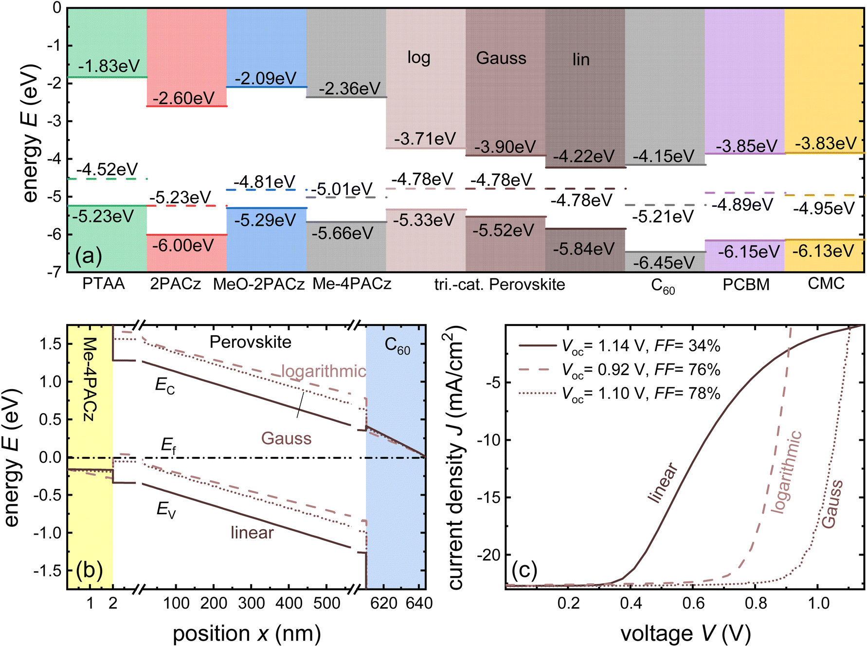 | ||
| Fig. 28 (a) Energy levels (EC, EF, EV relative to the vacuum level) for different HTLs, perovskite layers deposited on Me-4PACz, and ETLs deposited on perovskite. For all transport layers, the linear method was used to determine the EV, whereas for the perovskite, we used three methods (linear, logarithmic, and Gaussian fitting). (b) Resulting band diagrams for the stack Me-4PACz/perovskite/C60 and three fitting methods. (c) Simulated current–voltage curves showing S-shapes for the linear method (extraction barrier towards C60) and strong losses in open-circuit voltage for the logarithmic method (large band offset towards C60). Figure reproduced from ref. 30 under the terms of the CC-BY 4.0 license. © The authors of ref. 30 (2023). | ||
6.2. Electrostatics and ion movement
Fig. 29 shows an example of such a measurement,162 whereby panels (a) to (d) show the photovoltaic parameters ((a) efficiency, (b) Jsc, (c) Voc, and (d) FF) as a function of scan rate (in V s−1) and as a function of aging time (see color of the lines and the legend in panel (b)). We note that at typical scan rates of 100 mV s−1 that are used for traditional JV-curve measurements, the difference between forward and reverse scan is minimal (left edge of the figures). The same is true for the fastest shown measurements. In an intermediate range of scan rates, however, the difference between forward and reverse scan has a maximum that is primarily caused by a huge discrepancy in FF (see panel (d)). This result is logical if we assume that for very slow scan speeds, the ions can follow the voltage, while for very fast scan speeds they will be fixed at the condition set before the scan started. These are the two situations labelled “steady state” and “ion freeze” in Fig. 29a. At an intermediate scan rate, the ions will move during the scan but will not have found a steady-state configuration, thereby leading to an efficiency that depends strongly on the scan direction (labelled as “peak hysteresis” in panel (a)).
 | ||
| Fig. 29 (a) Efficiency (b) Jsc, (c) Voc, and (d) FF as a function of scan rate and degradation time for a triple-cation perovskite solar cell. (e) Efficiency loss as a function of ageing time, whereby the losses are split up in ionic losses (see panel (a)) and fast losses, i.e. the losses at the high scan rate condition. (f) Current–voltage curves after 480 min of ageing as a function of scan rate. Figure reproduced from ref. 162 under the terms of the CC-BY 4.0 license. © The authors of ref. 162 (2024). | ||
The second observation is about long-term degradation and is summarized in panel (e) which shows that degradation primarily affects the steady state efficiency but less so the efficiency at the ion-freeze condition of fast scan rates. Thus, these results suggest that the major contribution to the degradation is at least related to the mobile ions as it shows up as a growing difference between the high and low scan rate efficiencies (labelled ionic loss in panel (a) and (e)).
The fast hysteresis measurement provides a remarkably simple approach to quantifying the effect of mobile ions on performance and degradation. Challenges associated with this type of measurement are primarily relevant for researchers who aim for more quantitative information on the ions themselves such as their diffusion coefficient and absolute densities. These properties will affect the fast hysteresis measurements, but they may not do so in a sufficiently unique way to be able to infer these parameters with certainty. For instance, Le Corre et al.167 show how the ion density and the ion diffusion coefficients affect the position and extent of the region of peak hysteresis (see Fig. 1d and e in ref. 167). Thus, additional measurements are likely beneficial to quantify e.g. ion densities. Conceivable approaches are to use variants of charge extraction methods such as BACE (bias-assisted charge extraction) or CELIV (charge extraction with linearly increasing voltage)42,90,167 that allow quantifying the ion density from the current extracted from the sample at longer times after the voltage step that triggers the charge extraction process. The frequency domain equivalent of these techniques is to quantify ion densities via the low frequency capacitance response as shown for instance by Diekmann et al.90 or by Diethelm et al.91
On the bright side, the topic of metastability is a thankful and popular topic for specialized papers that focus on the phenomena rather than technology development. There are a couple of recent findings that I would like to highlight as an outlook to show possible future developments. The paper by Thiesbrummel et al.162 already featured before, is significant as it applies a reasonably simple method to relevant samples and shows that the ions are strongly affecting degradation. A somewhat related finding was recently reported by Jiang et al.168 showing how ions and their interaction with electron and hole transport layers affect degradation under reverse bias stress. A related work by Li et al.169 showed that the detrimental effects of reverse bias can be mitigated by ion diffusion barriers consisting (in this case) of SnO2 layers. Especially, the combination SnO2/ITO that is commonly used in tandem solar cells yields significant stability advantages that are consistent with the high reverse bias stability seen in silicon-perovskite tandem solar cells.170
In addition to obtaining further insights into the degradation mechanism, there are also methodological innovations within the field. In addition to the example of the fast hysteresis measurement, a somewhat complementary technique recently developed by Hill et al.171 is the stabilize and pulse experiment. Rather than going through all different scan rates, the focus in this experiment is to put a larger emphasis on the prebias condition (stabilizing phase) and then measure the JV curve using a series of fast voltage pulses. To better explain the influence of ions, the combination of these experimental methods with drift-diffusion simulations that explicitly consider ion movement is highly beneficial.172
7. Outlook and conclusions
The state of the research community working on the device physics of halide perovskites can be best understood by comparison with crystalline silicon. In the case of silicon, many material properties have been determined over the years, which implies that sophisticated parameterisations such as mobility173 or Auger coefficients as functions of doping density174 or (in the latter case) excess carrier density exist and can be used in simulation software.173 In the world of crystalline Si, relevant variations can include the type of wafer (for example, Czochralski vs. floatzone), the doping type and density, and the surface texture and passivation. Often, surface passivation has the most significant influence on the charge carrier lifetimes, while the mobilities are largely known. There wouldn't even be a need to experimentally determine them anymore if the doping density is known. Wafer characterization for the purpose of solar cell development can therefore focus on the measurement of minority carrier lifetimes using e.g. the quasi-steady-state photoconductivity method175 possibly combined with optical characterization of the passivation and transport layers to quantify possible parasitic absorption losses.176In the world of halide perovskite research, it is often not even clear what kind of model one would have to use for a given simulation or attempt to data extraction.23 Furthermore, the huge variety of different compositions, different surface passivations and treatments as well as different characterisation methods lead to the unfortunate situation that even for a given sample, there is rarely such a thing as a well-defined parameter such as lifetime or mobility. However, it is possible to measure samples using different techniques, extract parameters from the observables, and then compare parameters obtained from different measurements to approach a consistent model and a consistent set of parameters that can describe the behaviour of the solar cell and can help in designing better solar cells.33,177,178 The development of measurements or variants of measurements that provide additional degrees of freedom is therefore important, as they will provide more measurement data to quantify the many unknowns that exist.179 Examples of additional degrees of freedom that have recently been explored are the different implementations of photo-Hall measurements,145,146 as well as variants of transient photoluminescence employing variations of repetition rate23 or the use of pulse bursts180,181 which are not commonly employed in the literature.
The article argues that one of the major obstacles towards this goal of determining a consistent set of parameters and using a consistent model is the step from the experimental observables (PL intensity, current, impedance, etc…) to the parameters (mobility, lifetime, surface recombination velocity, etc…).179 This step requires either an analytical or numerical approach. As most analytical equations are valid only within a limited parameter range,29,89,182 the sensible choice is often the numerical approach to data analysis.40,111,183 However, this approach has the decisive disadvantage that data analysis might become a chicken- and egg-type problem as one parameter will depend on another. Eventually, the problem will boil down to the determination of several unknowns using several experimental datasets and a global model that should describe all experimental datasets simultaneously. Such approaches have been applied to halide perovskite research in the past,33,177,178 but examples are rather scarce, given the relatively large effort associated with such global fits. Thus, future research should focus on data analysis methods that significantly speed up the analysis of several experimental datasets using a global model with several unknowns. Approaches employing the tool set of Bayesian statistics and Bayesian parameter inference exist,41,184 and first approaches to apply them to halide perovskites have been published.40,111,179 However, this field is currently still in its infancy. The rapid developments in the general field of machine learning methods provide some hope that data analysis methods based on sensible numerical models will become more usable and more widely applied within the community and may be able to overcome the current tendency to use overly simplified analytical models.
Beyond the prospect of better data analysis methods to be implemented in the future, this article provides a summary of the major challenges that researchers face when applying different methods and possibilities to overcome or mitigate the challenges that can be implemented without the need for additional developments. Table 3 goes back to the discussion in the introduction and provides a new column as compared to Table 1 that summarises the opportunities and safeguards that are recommended to either verify the validity of certain data analysis approaches (e.g. the case of SCLC or capacitance measurements), provide alternative analytical equations (e.g. the case of transient photovoltage or photoluminescence), suggest less common variants of measurements to obtain additional information (see the use of the peak shift in transient photoluminescence), or suggest specific combinations of measurements that are not commonly used in the literature to verify or falsify certain conclusions (see, e.g. the chapter on photoelectron spectroscopy). Many, but certainly not all, of the methods discussed here tend to be on the less expensive end of equipment costs such that their application is or could be rather widespread.
| Quantity | Method | Opportunities and safeguards |
|---|---|---|
| Defect density | Trap filled current in single carrier devices | Measure built-in voltage using all four branches of the JV-curve (up, down, forward, reverse)30,80 |
| Capacitance based methods | Consider detection threshold,72 study lateral devices121 or thick devices86 | |
| Lifetime | Transient photoluminescence | Determine recombination coefficient from power law shaped decays25 |
| Use low repetition rates. Vary repetition rates or use complex pulse sequences23,180 | ||
| Transient photovoltage | Combine rise and decay of photovoltage17 | |
| Impedance | Vary voltage or light intensity. Use matrix model27 for data analysis | |
| Doping | Capacitance, Mott–Schottky | Consider detection threshold.72 Include ionic contributions in numerical simulations91 |
| Energy levels | Photoelectron spectroscopy | Complement with device simulation as well as with complementary methods such as SCLC30 |
| Mobility | SCLC, TPC | Remove contact layer or account for contact layers in data analysis30 |
| Photoluminescence | Exploit peak shift to determine out-of-plane mobilities32 | |
| Charge transfer and extraction | Transient PL on bilayers | Vary laser fluence. Use numerical methods for data analysis34 |
| Voltage dependent PL | Vary properties of ETL or HTL to isolate the extraction-limiting interface104,126,127 |
Finally, Fig. 30 aims to summarize the main message of the study in a more abstract manner. Meaningful characterization of samples within any research field requires a good match between the sample, the experiment and the data analysis method. The experiment and the data analysis approach must consider the properties of the sample. In the case of halide perovskites, parameters and properties are so difficult to classical semiconductors such as silicon that often either the experiment or the data analysis method are inapplicable to the sample. Thus, solutions as presented in this article will always provide either more adequate experimental methods or variants of existing methods or analysis methods that are better adapted to the expected sample properties.
 | ||
| Fig. 30 A good experiment requires a match between the sample and its properties (e.g. thickness, presence of ions, low doping density), the experiment, and the data analysis (analytical, numerical). Many problems within the field of halide perovskites can be summarized by a mismatch between these three, whereby the typical problems are that an inadequate data analysis is used that does not consider the specific properties of halide perovskites or that an altogether inadequate experiment is used that is not sensitive to the desired material parameters. The solutions and opportunities discussed in this perspective therefore aim to provide solutions to either of these challenges. | ||
Data availability
No new data is associated with this work.Author contributions
TK wrote the article.Conflicts of interest
The author declares no competing financial or non-financial interests.Acknowledgements
TK acknowledges funding from the Helmholtz Association via the POF IV and from the DFG for the project CREATIVE within the SPP “Perovskite Semiconductors: From Fundamental Properties to Devices” (SPP 2196). Open-access publication was funded by the German Research Foundation (DFG) 491111487.References
- H. Zhu, S. Teale, M. N. Lintangpradipto, S. Mahesh, B. Chen, M. D. McGehee, E. H. Sargent and O. M. Bakr, Nat. Rev. Mater., 2023, 8, 569–586 CrossRef.
- L. Duan, D. Walter, N. Chang, J. Bullock, D. Kang, S. P. Phang, K. Weber, T. White, D. Macdonald, K. Catchpole and H. Shen, Nat. Rev. Mater., 2023, 8, 261–281 CrossRef CAS.
- K. J. Prince, H. M. Mirletz, E. A. Gaulding, L. M. Wheeler, R. A. Kerner, X. Zheng, L. T. Schelhas, P. Tracy, C. A. Wolden, J. J. Berry, S. Ovaitt, T. M. Barnes and J. M. Luther, Nat. Mater., 2024, 24, 22–33 CrossRef PubMed.
- P. V. Kamat, ACS Energy Lett., 2025, 10, 896–897 CrossRef CAS.
- Z. Liang, Y. Zhang, H. Xu, W. Chen, B. Liu, J. Zhang, H. Zhang, Z. Wang, D.-H. Kang, J. Zeng, X. Gao, Q. Wang, H. Hu, H. Zhou, X. Cai, X. Tian, P. Reiss, B. Xu, T. Kirchartz, Z. Xiao, S. Dai, N.-G. Park, J. Ye and X. Pan, Nature, 2023, 624, 557–563 CrossRef CAS PubMed.
- G. Li, Z. Su, L. Canil, D. Hughes, M. H. Aldamasy, J. Dagar, S. Trofimov, L. Wang, W. Zuo, J. J. Jerónimo-Rendon, M. M. Byranvand, C. Wang, R. Zhu, Z. Zhang, F. Yang, G. Nasti, B. Naydenov, W. C. Tsoi, Z. Li, X. Gao, Z. Wang, Y. Jia, E. Unger, M. Saliba, M. Li and A. Abate, Science, 2023, 379, 399–403 CrossRef CAS PubMed.
- S. Tan, T. Huang, I. Yavuz, R. Wang, T. W. Yoon, M. Xu, Q. Xing, K. Park, D.-K. Lee, C.-H. Chen, R. Zheng, T. Yoon, Y. Zhao, H.-C. Wang, D. Meng, J. Xue, Y. J. Song, X. Pan, N.-G. Park, J.-W. Lee and Y. Yang, Nature, 2022, 605, 268–273 CrossRef CAS PubMed.
- H. Chen, A. Maxwell, C. Li, S. Teale, B. Chen, T. Zhu, E. Ugur, G. Harrison, L. Grater, J. Wang, Z. Wang, L. Zeng, S. M. Park, L. Chen, P. Serles, R. A. Awni, B. Subedi, X. Zheng, C. Xiao, N. J. Podraza, T. Filleter, C. Liu, Y. Yang, J. M. Luther, S. De Wolf, M. G. Kanatzidis, Y. Yan and E. H. Sargent, Nature, 2023, 613, 676–681 CrossRef CAS.
- R. Lin, J. Xu, M. Wei, Y. Wang, Z. Qin, Z. Liu, J. Wu, K. Xiao, B. Chen, S. M. Park, G. Chen, H. R. Atapattu, K. R. Graham, J. Xu, J. Zhu, L. Li, C. Zhang, E. H. Sargent and H. Tan, Nature, 2022, 603, 73–78 CrossRef CAS PubMed.
- T. Li, J. Xu, R. Lin, S. Teale, H. Li, Z. Liu, C. Duan, Q. Zhao, K. Xiao, P. Wu, B. Chen, S. Jiang, S. Xiong, H. Luo, S. Wan, L. Li, Q. Bao, Y. Tian, X. Gao, J. Xie, E. H. Sargent and H. Tan, Nat. Energy, 2023, 8, 610–620 CrossRef CAS.
- S. Teale, M. Degani, B. Chen, E. H. Sargent and G. Grancini, Nat. Energy, 2024, 9, 779–792 CrossRef CAS.
- R. He, W. Wang, Z. Yi, F. Lang, C. Chen, J. Luo, J. Zhu, J. Thiesbrummel, S. Shah, K. Wei, Y. Luo, C. Wang, H. Lai, H. Huang, J. Zhou, B. Zou, X. Yin, S. Ren, X. Hao, L. Wu, J. Zhang, J. Zhang, M. Stolterfoht, F. Fu, W. Tang and D. Zhao, Nature, 2023, 618, 80–86 CrossRef CAS PubMed.
- Z. Liu, J. Siekmann, B. Klingebiel, U. Rau and T. Kirchartz, Adv. Energy Mater., 2021, 11, 2003386 CrossRef CAS.
- J. Li, H. Liang, C. Xiao, X. Jia, R. Guo, J. Chen, X. Guo, R. Luo, X. Wang, M. Li, M. Rossier, A. Hauser, F. Linardi, E. Alvianto, S. Liu, J. Feng and Y. Hou, Nat. Energy, 2024, 9, 308–315 CrossRef CAS.
- A. Al-Ashouri, A. Magomedov, M. Roß, M. Jošt, M. Talaikis, G. Chistiakova, T. Bertram, J. A. Márquez, E. Köhnen, E. Kasparavičius, S. Levcenco, L. Gil-Escrig, C. J. Hages, R. Schlatmann, B. Rech, T. Malinauskas, T. Unold, C. A. Kaufmann, L. Korte, G. Niaura, V. Getautis and S. Albrecht, Energy Environ. Sci., 2019, 12, 3356–3369 RSC.
- S. Mariotti, E. Köhnen, F. Scheler, K. Sveinbjörnsson, L. Zimmermann, M. Piot, F. Yang, B. Li, J. Warby, A. Musiienko, D. Menzel, F. Lang, S. Keßler, I. Levine, D. Mantione, A. Al-Ashouri, M. S. Härtel, K. Xu, A. Cruz, J. Kurpiers, P. Wagner, H. Köbler, J. Li, A. Magomedov, D. Mecerreyes, E. Unger, A. Abate, M. Stolterfoht, B. Stannowski, R. Schlatmann, L. Korte and S. Albrecht, Science, 2023, 381, 63–69 CrossRef CAS PubMed.
- L. Krückemeier, Z. Liu, T. Kirchartz and U. Rau, Adv. Mater., 2023, 35, 2300872 CrossRef PubMed.
- Y. N. Harari, Nexus: A Brief History of Information Networks from the Stone Age to AI, Random House, New York, 2024 Search PubMed.
- V. M. Le Corre, J. Phys. Chem. Lett., 2024, 15, 10001–10008 CrossRef CAS PubMed.
- T. Kirchartz, Beilstein J. Nanotechnol., 2013, 4, 180–188 CrossRef CAS PubMed.
- S. Ravishankar, T. Unold and T. Kirchartz, Science, 2021, 371, eabd8014 CrossRef CAS PubMed.
- Y. Yuan, G. Yan, C. Dreessen, T. Rudolph, M. Hülsbeck, B. Klingebiel, J. Ye, U. Rau and T. Kirchartz, Nat. Mater., 2024, 23, 391–397 CrossRef CAS PubMed.
- A. Kiligaridis, P. A. Frantsuzov, A. Yangui, S. Seth, J. Li, Q. An, Y. Vaynzof and I. G. Scheblykin, Nat. Commun., 2021, 12, 3329 CrossRef CAS PubMed.
- M. J. Trimpl, A. D. Wright, K. Schutt, L. R. V. Buizza, Z. Wang, M. B. Johnston, H. J. Snaith, P. Müller-Buschbaum and L. M. Herz, Adv. Funct. Mater., 2020, 30, 2004312 CrossRef CAS.
- Y. Yuan, G. Yan, C. Dreessen and T. Kirchartz, Adv. Energy Mater., 2025, 15, 2403279 CrossRef CAS.
- D. Kiermasch, A. Baumann, M. Fischer, V. Dyakonov and K. Tvingstedt, Energy Environ. Sci., 2018, 11, 629–640 RSC.
- S. Ravishankar, Z. Liu, Y. Wang, T. Kirchartz and U. Rau, PRX Energy, 2023, 2, 033006 CrossRef.
- S. Ravishankar, L. Kruppa, S. Jenatsch, G. Yan and Y. Wang, Energy Environ. Sci., 2024, 17, 1229–1243 RSC.
- T. Kirchartz, W. Gong, S. A. Hawks, T. Agostinelli, R. C. I. MacKenzie, Y. Yang and J. Nelson, J. Phys. Chem. C, 2012, 116, 7672–7680 CrossRef CAS.
- J. Siekmann, A. Kulkarni, S. Akel, B. Klingebiel, M. Saliba, U. Rau and T. Kirchartz, Adv. Energy Mater., 2023, 13, 2300448 CrossRef CAS.
- D. Menzel, A. Tejada, A. Al-Ashouri, I. Levine, J. A. Guerra, B. Rech, S. Albrecht and L. Korte, ACS Appl. Mater. Interfaces, 2021, 13, 43540–43553 CrossRef CAS.
- C. Cho, S. Feldmann, K. M. Yeom, Y.-W. Jang, S. Kahmann, J.-Y. Huang, T. C. J. Yang, M. N. T. Khayyat, Y.-R. Wu, M. Choi, J. H. Noh, S. D. Stranks and N. C. Greenham, Nat. Mater., 2022, 21, 1388–1395 CrossRef CAS PubMed.
- L. Krückemeier, B. Krogmeier, Z. Liu, U. Rau and T. Kirchartz, Adv. Energy Mater., 2021, 11, 2003489 CrossRef.
- B. Krogmeier, F. Staub, D. Grabowski, U. Rau and T. Kirchartz, Sustainable Energy Fuels, 2018, 2, 1027–1034 RSC.
- W. Tress, Adv. Energy Mater., 2017, 7, 1602358 CrossRef.
- L. Krückemeier, Z. Liu, B. Krogmeier, U. Rau and T. Kirchartz, Adv. Energy Mater., 2021, 11, 2102290 CrossRef.
- P. Calado, D. Burkitt, J. Yao, J. Troughton, T. M. Watson, M. J. Carnie, A. M. Telford, B. C. O'Regan, J. Nelson and P. R. F. Barnes, Phys. Rev. Appl., 2019, 11, 044005 CrossRef CAS.
- R. A. Belisle, W. H. Nguyen, A. R. Bowring, P. Calado, X. Li, S. J. C. Irvine, M. D. McGehee, P. R. F. Barnes and B. C. O'Regan, Energy Environ. Sci., 2017, 10, 192–204 RSC.
- M. H. Futscher and C. Deibel, ACS Energy Lett., 2022, 7, 140–144 CrossRef CAS.
- C. Fai, A. J. C. Ladd and C. J. Hages, Joule, 2022, 6, 2585–2610 CrossRef CAS.
- R. E. Brandt, R. C. Kurchin, V. Steinmann, D. Kitchaev, C. Roat, S. Levcenco, G. Ceder, T. Unold and T. Buonassisi, Joule, 2017, 1, 843–856 CrossRef.
- F. Peña-Camargo, J. Thiesbrummel, H. Hempel, A. Musiienko, V. M. L. Corre, J. Diekmann, J. Warby, T. Unold, F. Lang, D. Neher and M. Stolterfoht, Appl. Phys. Rev., 2022, 9, 021409 Search PubMed.
- K. Frohna, M. Anaya, S. Macpherson, J. Sung, T. A. S. Doherty, Y.-H. Chiang, A. J. Winchester, K. W. P. Orr, J. E. Parker, P. D. Quinn, K. M. Dani, A. Rao and S. D. Stranks, Nat. Nanotechnol., 2022, 17, 190–196 CrossRef CAS.
- S. Feldmann, S. Macpherson, S. P. Senanayak, M. Abdi-Jalebi, J. P. H. Rivett, G. Nan, G. D. Tainter, T. A. S. Doherty, K. Frohna, E. Ringe, R. H. Friend, H. Sirringhaus, M. Saliba, D. Beljonne, S. D. Stranks and F. Deschler, Nat. Photonics, 2020, 14, 123–128 CrossRef CAS.
- K. Frohna, C. Chosy, A. Al-Ashouri, F. Scheler, Y.-H. Chiang, M. Dubajic, J. E. Parker, J. M. Walker, L. Zimmermann, T. A. Selby, Y. Lu, B. Roose, S. Albrecht, M. Anaya and S. D. Stranks, Nat. Energy, 2025, 10, 66–76 CrossRef CAS PubMed.
- T. Kirchartz and U. Rau, Adv. Energy Mater., 2018, 8, 1703385 CrossRef.
- V. M. Le Corre, M. L. C. Koopmans and L. J. A. Koster, J. Open Source Softw., 2022, 7, 3727 CrossRef.
- P. Calado, I. Gelmetti, B. Hilton, M. Azzouzi, J. Nelson and P. R. F. Barnes, J. Comput. Electron., 2022, 21, 960–991 CrossRef CAS.
- W. Clarke, L. J. Bennett, Y. Grudeva, J. M. Foster, G. Richardson and N. E. Courtier, J. Comput. Electron., 2023, 22, 364–382 CAS.
- R. C. I. MacKenzie, T. Kirchartz, G. F. A. Dibb and J. Nelson, J. Phys. Chem. C, 2011, 115, 9806–9813 CrossRef CAS.
- M. Burgelman, J. Verschraegen, S. Degrave and P. Nollet, Prog. Photovoltaics, 2004, 12, 143–153 CAS.
- M. Burgelman, P. Nollet and S. Degrave, Thin Solid Films, 2000, 361, 527–532 CrossRef.
- R. E. I. Schropp and M. Zeman, Amorphous and Microcrystalline Silicon Solar Cells: Modeling, Materials and Device Technology, Springer, 1998 Search PubMed.
- B. E. Pieters, J. Krc and M. Zeman, Conference Record of the 2006 IEEE 4th World Conference on Photovoltaic Energy Conversion, Waikoloa, Hawaii Search PubMed.
- T. Kirchartz, B. E. Pieters, J. Kirkpatrick, U. Rau and J. Nelson, Phys. Rev. B: Condens. Matter Mater. Phys., 2011, 83, 115209 CrossRef.
- B. E. Pieters, K. Decock, M. Burgelman, R. Stangl and T. Kirchartz, in Advanced Characterization Techniques for Thin Film Solar Cells, ed. D. Abou-Ras, T. Kirchartz and U. Rau, Wiley-VCH Verlag GmbH & Co. KGaA, 2011, pp. 501–527, DOI:10.1002/9783527636280.ch19.
- T. Kirchartz, L. Krückemeier and E. L. Unger, APL Mater., 2018, 6, 100702 CrossRef.
- S. C. Gillespie, J. Gautier, J. S. van der Burgt, J. Anker, B. L. J. Geerligs, G. Coletti and E. C. Garnett, Adv. Energy Mater., 2024, 14, 2400965 CrossRef CAS.
- S. Jariwala, S. Burke, S. Dunfield, R. C. Shallcross, M. Taddei, J. Wang, G. E. Eperon, N. R. Armstrong, J. J. Berry and D. S. Ginger, Chem. Mater., 2021, 33, 5035–5044 CrossRef CAS.
- J. Wang, W. Fu, S. Jariwala, I. Sinha, A. K.-Y. Jen and D. S. Ginger, ACS Energy Lett., 2018, 4, 222–227 CrossRef.
- J. Haddad, B. Krogmeier, B. Klingebiel, L. Krückemeier, S. Melhem, Z. Liu, J. Hüpkes, S. Mathur and T. Kirchartz, Adv. Mater. Interfaces, 2020, 7, 2000366 CrossRef CAS.
- C. Eames, J. M. Frost, P. R. F. Barnes, B. C. OGÇÖRegan, A. Walsh and M. S. Islam, Nat. Commun., 2015, 6, 7497 CrossRef CAS PubMed.
- P. Calado, A. M. Telford, D. Bryant, X. Li, J. Nelson, B. C. O'Regan and P. R. F. Barnes, Nat. Commun., 2016, 7, 13831 CrossRef CAS PubMed.
- D. Moia and J. Maier, ACS Energy Lett., 2021, 6, 1566–1576 CrossRef CAS.
- G. Y. Kim, A. Senocrate, T.-Y. Yang, G. Gregori, M. Grätzel and J. Maier, Nat. Mater., 2018, 17, 445–449 CrossRef CAS PubMed.
- D. Moia, I. Gelmetti, P. Calado, W. Fisher, M. Stringer, O. Game, Y. Hu, P. Docampo, D. Lidzey, E. Palomares, J. Nelson and P. R. F. Barnes, Energy Environ. Sci., 2019, 12, 1296–1308 RSC.
- N. Tessler and Y. Vaynzof, ACS Energy Lett., 2020, 5, 1260–1270 CrossRef CAS.
- P. Lopez-Varo, J. A. Jiménez-Tejada, M. García-Rosell, S. Ravishankar, G. Garcia-Belmonte, J. Bisquert and O. Almora, Adv. Energy Mater., 2018, 8, 1702772 CrossRef.
- N. E. Courtier, J. M. Cave, J. M. Foster, A. B. Walker and G. Richardson, Energy Environ. Sci., 2019, 12, 396–409 RSC.
- S. M. Sze, Physics of Semiconductor Devices, John Wiley & Sons, New York, 2nd edn, 1981 Search PubMed.
- T. Kirchartz, A. Helbig and U. Rau, Sol. Energy Mater. Sol. Cells, 2008, 92, 1621–1627 CrossRef CAS.
- J. Siekmann, S. Ravishankar and T. Kirchartz, ACS Energy Lett., 2021, 6, 3244–3251 CrossRef CAS.
- T. Kirchartz, Philos. Trans. R. Soc., A, 2019, 377, 20180286 CrossRef.
- M. A. Lampert, Rep. Prog. Phys., 1964, 27, 329 CrossRef CAS.
- M. A. Faist, S. Shoaee, S. M. Tuladhar, G. F. A. Dibb, S. Foster, W. Gong, T. Kirchartz, D. D. C. Bradley, J. R. Durrant and J. Nelson, Adv. Energy Mater., 2013, 3, 744–752 CrossRef CAS.
- H. K. H. Lee, A. M. Telford, J. A. Rohr, M. F. Wyatt, B. Rice, J. Wu, A. de Castro Maciel, S. M. Tuladhar, E. Speller, J. McGettrick, J. R. Searle, S. Pont, T. Watson, T. Kirchartz, J. R. Durrant, W. C. Tsoi, J. Nelson and Z. Li, Energy Environ. Sci., 2018, 11, 417–428 RSC.
- J. A. Röhr, T. Kirchartz and J. Nelson, J. Phys.: Condens. Matter, 2017, 29, 205901 CrossRef PubMed.
- J. A. Röhr, D. Moia, S. A. Haque, T. Kirchartz and J. Nelson, J. Phys.: Condens. Matter, 2018, 30, 105901 CrossRef PubMed.
- V. Bruevich, H. H. Choi and V. Podzorov, Adv. Funct. Mater., 2021, 31, 2006178 CrossRef CAS.
- J. A. Röhr, Phys. Rev. Appl., 2019, 11, 054079 CrossRef.
- M. A. Lampert, Phys. Rev., 1956, 103, 1648–1656 CrossRef CAS.
- E. A. Duijnstee, J. M. Ball, V. M. Le Corre, L. J. A. Koster, H. J. Snaith and J. Lim, ACS Energy Lett., 2020, 5, 376–384 CrossRef CAS.
- V. M. Le Corre, E. A. Duijnstee, O. El Tambouli, J. M. Ball, H. J. Snaith, J. Lim and L. J. A. Koster, ACS Energy Lett., 2021, 6, 1087–1094 CrossRef CAS.
- J. Heath and P. Zabierowski, in Advanced Characterization Techniques for Thin Film Solar Cells, ed. D. Abou-Ras, T. Kirchartz and U. Rau, Wiley-Vch, Weinheim, 2011, ch. 4, pp. 81–105 Search PubMed.
- T. Walter, R. Herberholz, C. Müller and H. W. Schock, J. Appl. Phys., 1996, 80, 4411–4420 CrossRef CAS.
- Z. Ni, C. Bao, Y. Liu, Q. Jiang, W.-Q. Wu, S. Chen, X. Dai, B. Chen, B. Hartweg, Z. Yu, Z. Holman and J. Huang, Science, 2020, 367, 1352–1358 CrossRef CAS PubMed.
- Y. Dou, S. Luo, P. Zhu, L. Zhu, G. Zhang, C. Bao, H. Yan, J. Zhu and S. Chen, Joule, 2025, 9, 101774 CrossRef CAS.
- S. Ravishankar, Z. Liu, U. Rau and T. Kirchartz, PRX Energy, 2022, 1, 013003 CrossRef.
- M. Fischer, K. Tvingstedt, A. Baumann and V. Dyakonov, ACS Appl. Energy Mater., 2018, 1, 5129–5134 CAS.
- J. Diekmann, F. Peña-Camargo, N. Tokmoldin, J. Thiesbrummel, J. Warby, E. Gutierrez-Partida, S. Shah, D. Neher and M. Stolterfoht, J. Phys. Chem. Lett., 2023, 14, 4200–4210 CrossRef CAS PubMed.
- M. Diethelm, T. Lukas, J. Smith, A. Dasgupta, P. Caprioglio, M. Futscher, R. Hany and H. J. Snaith, Energy Environ. Sci., 2025, 18, 1385–1397 RSC.
- A. A. Bakulin, A. Rao, V. G. Pavelyev, P. H. M. van Loosdrecht, M. S. Pshenichnikov, D. Niedzialek, J. Cornil, D. Beljonne and R. H. Friend, Science, 2012, 335, 1340–1344 CrossRef CAS.
- J. Pan, Z. Chen, T. Zhang, B. Hu, H. Ning, Z. Meng, Z. Su, D. Nodari, W. Xu, G. Min, M. Chen, X. Liu, N. Gasparini, S. A. Haque, P. R. F. Barnes, F. Gao and A. A. Bakulin, Nat. Commun., 2023, 14, 8000 CrossRef CAS PubMed.
- I. L. Braly, D. W. deQuilettes, L. M. Pazos-Outon, S. Burke, M. E. Ziffer, D. S. Ginger and H. W. Hillhouse, Nat. Photonics, 2018, 12, 355–361 CrossRef CAS.
- M. Stolterfoht, M. Grischek, P. Caprioglio, C. M. Wolff, E. Gutierrez-Partida, F. Peña-Camargo, D. Rothhardt, S. Zhang, M. Raoufi, J. Wolansky, M. Abdi-Jalebi, S. D. Stranks, S. Albrecht, T. Kirchartz and D. Neher, Adv. Mater., 2020, 32, 2000080 CrossRef CAS PubMed.
- M. Stolterfoht, P. Caprioglio, C. M. Wolff, J. A. Marquez, J. Nordmann, S. Zhang, D. Rothhardt, U. Hörmann, Y. Amir, A. Redinger, L. Kegelmann, F. Zu, S. Albrecht, N. Koch, T. Kirchartz, M. Saliba, T. Unold and D. Neher, Energy Environ. Sci., 2019, 12, 2778–2788 RSC.
- G. J. W. Aalbers, W. H. M. Remmerswaal, R. H. C. van den Heuvel, L. Bellini, L. M. Kessels, C. H. L. Weijtens, N. R. M. Schipper, M. M. Wienk and R. A. J. Janssen, J. Phys. Chem. Lett., 2025, 16, 372–377 CrossRef CAS PubMed.
- Y. Shi, E. Rojas-Gatjens, J. Wang, J. Pothoof, R. Giridharagopal, K. Ho, F. Jiang, M. Taddei, Z. Yang, E. M. Sanehira, M. D. Irwin, C. Silva-Acuña and D. S. Ginger, ACS Energy Lett., 2022, 7, 4081–4088 CrossRef CAS.
- D. W. deQuilettes, S. Koch, S. Burke, R. K. Paranji, A. J. Shropshire, M. E. Ziffer and D. S. Ginger, ACS Energy Lett., 2016, 1, 438–444 CrossRef CAS.
- K. Suchan, T. J. Jacobsson, C. Rehermann, E. L. Unger, T. Kirchartz and C. M. Wolff, Adv. Energy Mater., 2024, 14, 2303420 CrossRef CAS.
- E. M. Y. Lee and W. A. Tisdale, J. Phys. Chem. C, 2015, 119, 9005–9015 CrossRef CAS.
- F. C. Jamieson, E. B. Domingo, T. McCarthy-Ward, M. Heeney, N. Stingelin and J. R. Durrant, Chem. Sci., 2012, 3, 485–492 RSC.
- E. M. Hutter, T. Kirchartz, B. Ehrler, D. Cahen and E. v. Hauff, Appl. Phys. Lett., 2020, 116, 100501 CrossRef CAS.
- S. Akel, Y. Wang, G. Yan, U. Rau and T. Kirchartz, Adv. Energy Mater., 2024, 14, 2401800 CrossRef CAS.
- S. D. Stranks, G. E. Eperon, G. Grancini, C. Menelaou, M. J. P. Alcocer, T. Leijtens, L. M. Herz, A. Petrozza and H. J. Snaith, Science, 2013, 342, 341–344 CrossRef CAS.
- P. Zeng, G. Feng, X. Cui and M. Liu, J. Phys. Chem. C, 2020, 124, 6290–6296 CrossRef CAS.
- Y. Wang, S. Akel, B. Klingebiel and T. Kirchartz, Adv. Energy Mater., 2024, 14, 2302614 CrossRef CAS.
- E. M. Hutter, J. J. Hofman, M. L. Petrus, M. Moes, R. D. Abellón, P. Docampo and T. J. Savenije, Adv. Energy Mater., 2017, 7, 1602349 CrossRef.
- J. E. Lee, S. G. Motti, R. D. J. Oliver, S. Yan, H. J. Snaith, M. B. Johnston and L. M. Herz, Adv. Funct. Mater., 2024, 34, 2401052 CrossRef CAS.
- E. Butler-Caddle, K. D. G. I. Jayawardena, A. Wijesekara, R. L. Milot and J. Lloyd-Hughes, Phys. Rev. Appl., 2024, 22, 024013 CrossRef CAS.
- C. Kupfer, V. M. Le Corre, C. Li, L. Lüer, K. Forberich, M. Kato, A. Osvet and C. J. Brabec, J. Mater. Chem. C, 2024, 12, 95–102 RSC.
- M. Kober-Czerny, A. Dasgupta, S. Seo, F. M. Rombach, D. P. McMeekin, H. Jin and H. J. Snaith, PRX Energy, 2025, 4, 013001 CrossRef.
- T. Kirchartz, J. A. Márquez, M. Stolterfoht and T. Unold, Adv. Energy Mater., 2020, 10, 1904134 CrossRef CAS.
- M. Stolterfoht, C. M. Wolff, J. A. Marquez, S. Zhang, C. J. Hages, D. Rothhardt, S. Albrecht, P. L. Burn, P. Meredith, T. Unold and D. Neher, Nat. Energy, 2018, 3, 847–854 CrossRef CAS.
- S. Ravishankar, A. Riquelme, S. K. Sarkar, M. Garcia-Batlle, G. Garcia-Belmonte and J. Bisquert, J. Phys. Chem. C, 2019, 123, 24995–25014 CrossRef CAS.
- S. Ravishankar, C. Aranda, S. Sanchez, J. Bisquert, M. Saliba and G. Garcia-Belmonte, J. Phys. Chem. C, 2019, 123, 6444–6449 CrossRef CAS.
- A. Guerrero, J. Bisquert and G. Garcia-Belmonte, Chem. Rev., 2021, 121, 14430–14484 CrossRef CAS PubMed.
- A. O. Alvarez, S. Ravishankar and F. Fabregat-Santiago, Small Methods, 2021, 5, 2100661 CrossRef CAS PubMed.
- J. Bisquert, J. Phys. Chem. Lett., 2022, 13, 7320–7335 CrossRef CAS PubMed.
- J. Bisquert and M. Janssen, J. Phys. Chem. Lett., 2021, 12, 7964–7971 CrossRef CAS PubMed.
- A. Bou, H. Āboliņš, A. Ashoka, H. Cruanyes, A. Guerrero, F. Deschler and J. Bisquert, ACS Energy Lett., 2021, 6, 2248–2255 CrossRef CAS PubMed.
- R. Brenes, D. Guo, A. Osherov, N. K. Noel, C. Eames, E. M. Hutter, S. K. Pathak, F. Niroui, R. H. Friend, M. S. Islam, H. J. Snaith, V. Buloviç, T. J. Savenije and S. D. Stranks, Joule, 2017, 1, 155–167 CrossRef CAS.
- F. Staub, H. Hempel, J.-C. Hebig, J. Mock, U. W. Paetzold, U. Rau, T. Unold and T. Kirchartz, Phys. Rev. Appl., 2016, 6, 044017 CrossRef.
- M. Stolterfoht, V. M. Le Corre, M. Feuerstein, P. Caprioglio, L. J. A. Koster and D. Neher, ACS Energy Lett., 2019, 2887–2892, DOI:10.1021/acsenergylett.9b02262.
- M. Stolterfoht, C. M. Wolff, Y. Amir, A. Paulke, L. Perdigon-Toro, P. Caprioglio and D. Neher, Energy Environ. Sci., 2017, 10, 1530–1539 RSC.
- S. Akel, A. Kulkarni, U. Rau and T. Kirchartz, PRX Energy, 2023, 2, 013004 CrossRef.
- D. Grabowski, Z. Liu, G. Schöpe, U. Rau and T. Kirchartz, Sol. RRL, 2022, 6, 2200507 CrossRef CAS.
- M. Koopmans and L. J. A. Koster, Sol. RRL, 2022, 6, 2200560 CrossRef CAS.
- J. Diekmann, P. Caprioglio, M. H. Futscher, V. M. Le Corre, S. Reichert, F. Jaiser, M. Arvind, L. P. Toro, E. Gutierrez-Partida, F. Peña-Camargo, C. Deibel, B. Ehrler, T. Unold, T. Kirchartz, D. Neher and M. Stolterfoht, Sol. RRL, 2021, 5, 2100219 CrossRef CAS.
- W. Xu, L. J. F. Hart, B. Moss, P. Caprioglio, T. J. Macdonald, F. Furlan, J. Panidi, R. D. J. Oliver, R. A. Pacalaj, M. Heeney, N. Gasparini, H. J. Snaith, P. R. F. Barnes and J. R. Durrant, Adv. Energy Mater., 2023, 13, 2301102 CrossRef CAS.
- E. Gutierrez-Partida, M. Rusu, F. Zu, M. Raoufi, J. Diekmann, N. Tokmoldin, J. Warby, D. Menzel, F. Lang, S. Shah, S. Shoaee, L. Korte, T. Unold, N. Koch, T. Kirchartz, D. Neher and M. Stolterfoht, ACS Appl. Mater. Interfaces, 2025, 17, 11176–11186 CrossRef CAS PubMed.
- I. Levine, A. Al-Ashouri, A. Musiienko, H. Hempel, A. Magomedov, A. Drevilkauskaite, V. Getautis, D. Menzel, K. Hinrichs, T. Unold, S. Albrecht and T. Dittrich, Joule, 2021, 5, 2915–2933 CrossRef CAS.
- Y. Yuan, G. Yan, R. Hong, Z. Liang and T. Kirchartz, Adv. Mater., 2022, 34, 2108132 CrossRef CAS PubMed.
- L. M. Herz, ACS Energy Lett., 2017, 2, 1539–1548 CrossRef CAS.
- H. Hempel, T. J. Savenjie, M. Stolterfoht, J. Neu, M. Failla, V. C. Paingad, P. Kužel, E. J. Heilweil, J. A. Spies, M. Schleuning, J. Zhao, D. Friedrich, K. Schwarzburg, L. D. A. Siebbeles, P. Dörflinger, V. Dyakonov, R. Katoh, M. J. Hong, J. G. Labram, M. Monti, E. Butler-Caddle, J. Lloyd-Hughes, M. M. Taheri, J. B. Baxter, T. J. Magnanelli, S. Luo, J. M. Cardon, S. Ardo and T. Unold, Adv. Energy Mater., 2022, 12, 2102776 CrossRef CAS.
- M. I. Saidaminov, K. Williams, M. Wei, A. Johnston, R. Quintero-Bermudez, M. Vafaie, J. M. Pina, A. H. Proppe, Y. Hou, G. Walters, S. O. Kelley, W. A. Tisdale and E. H. Sargent, Nat. Mater., 2020, 19, 412–418 CrossRef CAS PubMed.
- L. M. Pazos-Outon, M. Szumilo, R. Lamboll, J. M. Richter, M. Crespo-Quesada, M. Abdi-Jalebi, H. J. Beeson, M. Vrucinic, M. Alsari, H. J. Snaith, B. Ehrler, R. H. Friend and F. Deschler, Science, 2016, 351, 1430–1433 CrossRef CAS PubMed.
- F. Staub, I. Anusca, D. C. Lupascu, U. Rau and T. Kirchartz, J. Phys. Mater., 2020, 3, 025003 CrossRef CAS.
- N. D. Arora, S. G. Chamberlain and D. J. Roulston, Appl. Phys. Lett., 1980, 37, 325–327 CrossRef CAS.
- R. Brendel and U. Rau, Solid State Phenom., 1999, 67–8, 81–86 Search PubMed.
- P. Würfel, T. Trupke, T. Puzzer, E. Schaffer, W. Warta and S. W. Glunz, J. Appl. Phys., 2007, 101, 123110 CrossRef.
- D. Hinken, K. Bothe, K. Ramspeck, S. Herlufsen and R. Brendel, J. Appl. Phys., 2009, 105, 104516 CrossRef.
- T. Kirchartz, A. Helbig, W. Reetz, M. Reuter, J. H. Werner and U. Rau, Prog. Photovoltaics, 2009, 17, 394–402 CAS.
- Y. Yuan, G. Yan, S. Akel, U. Rau and T. Kirchartz, Sci. Adv., 2025, 11, eadt1171 CrossRef CAS.
- A. Musiienko, F. Yang, T. W. Gries, C. Frasca, D. Friedrich, A. Al-Ashouri, E. Sağlamkaya, F. Lang, D. Kojda, Y.-T. Huang, V. Stacchini, R. L. Z. Hoye, M. Ahmadi, A. Kanak and A. Abate, Nat. Commun., 2024, 15, 316 CrossRef CAS PubMed.
- O. Gunawan, S. R. Pae, D. M. Bishop, Y. Virgus, J. H. Noh, N. J. Jeon, Y. S. Lee, X. Shao, T. Todorov, D. B. Mitzi and B. Shin, Nature, 2019, 575, 151–155 CrossRef CAS PubMed.
- V. Bruevich and V. Podzorov, Nat. Electron., 2024, 7, 510–512 CrossRef.
- R. Brüggemann, in Advanced Characterization Techniques for Thin Film Solar Cells, 2016, pp. 163–188, DOI:10.1002/9783527699025.ch7.
- I. Levine, S. Gupta, T. M. Brenner, D. Azulay, O. Millo, G. Hodes, D. Cahen and I. Balberg, J. Phys. Chem. Lett., 2016, 7, 5219–5226 CrossRef CAS PubMed.
- C. Longeaud, F. J. Ramos, A. Rebai and J. Rousset, Sol. RRL, 2018, 2, 1800192 CrossRef.
- R. Brenes, D. W. deQuilettes, R. Swartwout, A. Y. Alsalloum, O. M. Bakr and V. Bulović, ACS Nano, 2025, 19, 4213–4221 CrossRef CAS PubMed.
- D. K. Schroder, in Semiconductor Material and Device Characterization, John Wiley & Sons, Hoboken, New Jersey, 2005, ch. 8, pp. 465–522, DOI:10.1002/0471749095.ch8.
- T. J. Savenije, D. Guo, V. M. Caselli and E. M. Hutter, Adv. Energy Mater., 2020, 10, 1903788 CrossRef CAS.
- E. Butler-Caddle, N. E. Grant, S. L. Pain, J. D. Murphy, K. D. G. I. Jayawardena and J. Lloyd-Hughes, Appl. Phys. Lett., 2023, 122, 012101 CrossRef CAS.
- D. H. K. Murthy, A. Melianas, Z. Tang, G. Juska, K. Arlauskas, F. L. Zhang, L. D. A. Siebbeles, O. Inganas and T. J. Savenije, Adv. Funct. Mater., 2013, 23, 4262–4268 CrossRef CAS.
- Y. Hu, E. M. Hutter, P. Rieder, I. Grill, J. Hanisch, M. F. Aygüler, A. G. Hufnagel, M. Handloser, T. Bein, A. Hartschuh, K. Tvingstedt, V. Dyakonov, A. Baumann, T. J. Savenije, M. L. Petrus and P. Docampo, Adv. Energy Mater., 2018, 8(16), 1703057 CrossRef.
- H. Hempel, C. J. Hages, R. Eichberger, I. Repins and T. Unold, Sci. Rep., 2018, 8, 14476 CrossRef PubMed.
- M. Sebastiani, L. Di Gaspare, G. Capellini, C. Bittencourt and F. Evangelisti, Phys. Rev. Lett., 1995, 75, 3352–3355 CrossRef CAS PubMed.
- S. Tao, I. Schmidt, G. Brocks, J. Jiang, I. Tranca, K. Meerholz and S. Olthof, Nat. Commun., 2019, 10, 2560 CrossRef PubMed.
- J. Liu, M. De Bastiani, E. Aydin, G. T. Harrison, Y. Gao, R. R. Pradhan, M. K. Eswaran, M. Mandal, W. Yan, A. Seitkhan, M. Babics, A. S. Subbiah, E. Ugur, F. Xu, L. Xu, M. Wang, A. u. Rehman, A. Razzaq, J. Kang, R. Azmi, A. A. Said, F. H. Isikgor, T. G. Allen, D. Andrienko, U. Schwingenschlögl, F. Laquai and S. De Wolf, Science, 2022, 377, 302–306 CrossRef CAS PubMed.
- C. Gehrmann and D. A. Egger, Nat. Commun., 2019, 10, 3141 CrossRef PubMed.
- J. Thiesbrummel, S. Shah, E. Gutierrez-Partida, F. Zu, F. Peña-Camargo, S. Zeiske, J. Diekmann, F. Ye, K. P. Peters, K. O. Brinkmann, P. Caprioglio, A. Dasgupta, S. Seo, F. A. Adeleye, J. Warby, Q. Jeangros, F. Lang, S. Zhang, S. Albrecht, T. Riedl, A. Armin, D. Neher, N. Koch, Y. Wu, V. M. Le Corre, H. Snaith and M. Stolterfoht, Nat. Energy, 2024, 9, 664–676 CrossRef CAS.
- S. N. Habisreutinger, N. K. Noel and H. J. Snaith, ACS Energy Lett., 2018, 3, 2472–2476 CrossRef CAS.
- J. J. de Boer and B. Ehrler, ACS Energy Lett., 2024, 9, 5787–5794 CrossRef CAS PubMed.
- J. Bisquert, Adv. Energy Mater., 2024, 14, 2400442 CrossRef CAS.
- J. Thiesbrummel, V. M. Le Corre, F. Peña-Camargo, L. Perdigón-Toro, F. Lang, F. Yang, M. Grischek, E. Gutierrez-Partida, J. Warby, M. D. Farrar, S. Mahesh, P. Caprioglio, S. Albrecht, D. Neher, H. J. Snaith and M. Stolterfoht, Adv. Energy Mater., 2021, 11, 2101447 CrossRef CAS.
- V. M. Le Corre, J. Diekmann, F. Peña-Camargo, J. Thiesbrummel, N. Tokmoldin, E. Gutierrez-Partida, K. P. Peters, L. Perdigón-Toro, M. H. Futscher, F. Lang, J. Warby, H. J. Snaith, D. Neher and M. Stolterfoht, Sol. RRL, 2022, 6, 2100772 CrossRef CAS.
- F. Jiang, Y. Shi, T. R. Rana, D. Morales, I. E. Gould, D. P. McCarthy, J. A. Smith, M. G. Christoforo, M. Y. Yaman, F. Mandani, T. Terlier, H. Contreras, S. Barlow, A. D. Mohite, H. J. Snaith, S. R. Marder, J. D. MacKenzie, M. D. McGehee and D. S. Ginger, Nat. Energy, 2024, 9, 1275–1284 CrossRef CAS.
- N. Li, Z. Shi, C. Fei, H. Jiao, M. Li, H. Gu, S. P. Harvey, Y. Dong, M. C. Beard and J. Huang, Nat. Energy, 2024, 9, 1264–1274 CrossRef CAS.
- Z. Xu, H. Bristow, M. Babics, B. Vishal, E. Aydin, R. Azmi, E. Ugur, B. K. Yildirim, J. Liu, R. A. Kerner, S. De Wolf and B. P. Rand, Joule, 2023, 7, 1992–2002 CrossRef CAS.
- N. S. Hill, M. V. Cowley, N. Gluck, M. H. Fsadni, W. Clarke, Y. Hu, M. J. Wolf, N. Healy, M. Freitag, T. J. Penfold, G. Richardson, A. B. Walker, P. J. Cameron and P. Docampo, Adv. Mater., 2023, 35, 2302146 CrossRef CAS PubMed.
- L. J. F. Hart, F. J. Angus, Y. Li, A. Khaleed, P. Calado, J. R. Durrant, A. B. Djurišić, P. Docampo and P. R. F. Barnes, Energy Environ. Sci., 2024, 17, 7107–7118 RSC.
- P. P. Altermatt, J. Comput. Electron., 2011, 10, 314–330 CrossRef.
- A. Richter, S. W. Glunz, F. Werner, J. Schmidt and A. Cuevas, Phys. Rev. B:Condens. Matter Mater. Phys., 2012, 86, 165202 CrossRef.
- R. A. Sinton and A. Cuevas, Appl. Phys. Lett., 1996, 69, 2510–2512 CrossRef CAS.
- M. Köhler, M. Pomaska, P. Procel, R. Santbergen, A. Zamchiy, B. Macco, A. Lambertz, W. Duan, P. Cao, B. Klingebiel, S. Li, A. Eberst, M. Luysberg, K. Qiu, O. Isabella, F. Finger, T. Kirchartz, U. Rau and K. Ding, Nat. Energy, 2021, 6, 529–537 CrossRef.
- T. S. Sherkar, C. Momblona, L. Gil-Escrig, H. J. Bolink and L. J. A. Koster, Adv. Energy Mater., 2017, 7, 1602432 CrossRef.
- M. T. Neukom, A. Schiller, S. Züfle, E. Knapp, J. Ávila, D. Pérez-del-Rey, C. Dreessen, K. P. S. Zanoni, M. Sessolo, H. J. Bolink and B. Ruhstaller, ACS Appl. Mater. Interfaces, 2019, 11, 23320–23328 CrossRef CAS.
- T. Kirchartz and B. Das, J. Phys.: Energy, 2023, 5, 031001 CAS.
- A. Marunchenko, J. Kumar, A. Kiligaridis, S. M. Rao, D. Tatarinov, I. Matchenya, E. Sapozhnikova, R. Ji, O. Telschow, J. Brunner, A. Yulin, A. Pushkarev, Y. Vaynzof and I. G. Scheblykin, J. Phys. Chem. Lett., 2024, 15, 6256–6265 CrossRef CAS PubMed.
- A. Marunchenko, J. Kumar, A. Kiligaridis, D. Tatarinov, A. Pushkarev, Y. Vaynzof and I. G. Scheblykin, ACS Energy Lett., 2024, 9, 2075–2082 CrossRef CAS.
- O. Almora, C. Aranda, E. Mas-Marzá and G. Garcia-Belmonte, Appl. Phys. Lett., 2016, 109, 173903 CrossRef.
- V. M. Le Corre, T. S. Sherkar, M. Koopmans and L. J. A. Koster, Cell Rep. Phys. Sci., 2021, 2, 100346 CrossRef CAS.
- Z. Ren, F. Oviedo, M. Thway, S. I. P. Tian, Y. Wang, H. Xue, J. Dario Perea, M. Layurova, T. Heumueller, E. Birgersson, A. G. Aberle, C. J. Brabec, R. Stangl, Q. Li, S. Sun, F. Lin, I. M. Peters and T. Buonassisi, npj Comput. Mater., 2020, 6, 9 CrossRef CAS.
| This journal is © The Royal Society of Chemistry 2025 |