
 Open Access Article
 This Open Access Article is licensed under a Creative Commons Attribution-Non Commercial 3.0 Unported Licence
Highly stable bismuth-chloride perovskite X-ray direct detectors with an ultralow detection limit†
Haoyu
Chen
ad,
Qingyun
Han
ad,
Haoming
Qin
b,
Yueqi
Shen
ad,
Huijun
Lv
ad,
Yan
Liu
ad,
Liping
Du
ad,
Yong
Wang
c,
Yihui
He
*b and
Weihua
Ning
 *ad
*ad
aJiangsu Key Laboratory for Carbon-Based Functional Materials & Devices, Institute of Functional Nano & Soft Materials (FUNSOM), Soochow University, Suzhou, 215123, P. R. China. E-mail: whning@suda.edu.cn
bState Key Laboratory of Radiation Medicine and Protection, Collaborative Innovation Center of Radiological Medicine of Jiangsu Higher Education Institutions, School for Radiological and Interdisciplinary Sciences (RAD-X), Soochow University, Suzhou 215123, P. R. China. E-mail: yhhe@suda.edu.cn
cState Key Laboratory of Silicon and Advanced Semiconductor Materials, School of Materials Science and Engineering, Hangzhou Global Scientific and Technological Innovation Center, Zhejiang University, Hangzhou 310027, P. R. China
dJiangsu Key Laboratory of Advanced Negative Carbon Technologies, Soochow University, Suzhou, 215123, P. R. China
First published on 13th February 2025
Abstract
The quest for highly sensitive and stable X-ray detectors has intensified, driven by diverse applications such as medical diagnostics and industrial inspection. Recent strides have been made in harnessing the potential of lead halide perovskites for radiation detection, thanks to their remarkable optoelectronic properties. However, the toxicity of Pb and intrinsic material instability restrict their practical applications as next-generation efficient detectors. Here, we have developed environment-friendly three-dimensional (3D) bismuth-chloride perovskites designed for highly sensitive and stable X-ray direct detection. By the introduction of monovalent Na+, one-dimensional (1D) Cs3Bi2Cl9 can be converted into high-quality 3D double perovskite Cs2NaBiCl6 characterized by excellent photophysical properties. Our investigation, combining X-ray photoelectron spectroscopy and temperature-dependent photoluminescence, reveals a modulated electronic dimension and a mitigated electron–phonon coupling effect in Cs2NaBiCl6. As such, the 3D Cs2NaBiCl6-based direct detectors achieve a high sensitivity of 354.5 μC Gy−1 cm−2 and an ultralow detection limit of 59.4 nGy s−1, with continuous on–off switching for 4500 s. Overall, our work provides a new direction for designing and developing lead-free perovskites to achieve highly sensitive X-ray detection with exceptional stability.
Introduction
X-ray detectors have attracted considerable attention for their wide range of applications in medical diagnostics, industrial non-destructive inspection, aerospace, high-energy physics, and scientific research.1–4 Compared to indirect methods involving the conversion of X-ray into photons through scintillation, followed by detection via photodiodes, direct conversion of X-rays into an electrical signal offers superior spatial resolution and a more streamlined system configuration.5–9 Currently, extensive research has focused on α-Se10,11 and CdZnTe12,13 semiconductors for their superior detection performance in the past few decades. However, these materials suffer from many limitations such as the poor X-ray absorption in α-Se11,14 and the high synthesis cost of CdZnTe.15 Recently, solution-processed Pb-based perovskites16–19 with low defect density, high carrier mobility, and long carrier diffusion lengths20 have been anticipated as the next generation of high-efficiency X-ray detectors. In particular, the reported radiation detectors based on three dimensional (3D) perovskites, such as MAPbBr3,21,22 MAPbI3 (ref. 23 and 24) and CsPbBr3 (ref. 25–28) have demonstrated encouraging and promising performance.Despite their enormous success, the toxic lead content20 and poor stability29 are major obstacles to future commercialization. To remedy both issues, the community has now made increasing efforts on lead-free perovskites. Among these,30–33 bismuth-based perovskites stand out for their substantial X-ray attenuation coefficient and stability. Recent reports on sensitive X-ray detectors employing either Cs2AgBiBr6 (ref. 34–36) or (NH4)3Bi2I9 (ref. 37) single crystals (SCs) have demonstrated sensitivity exceeding 103 μC Gy−1 cm−2, outperforming commercial X-ray detectors. However, these detectors based on bismuth-bromide/iodide perovskite suffer from baseline drift and significant noise. Furthermore, the inherent chemical properties of bismuth make it challenging to form high-dimensional structures, resulting in poor charge carrier transport.38–41 These offer significant potential to improve the performance of bismuth-based perovskites. Chlorides emerge as an ideal solution, offering high stability and a wide bandgap.42 Our previous work confirms that replacing two Pb atoms with a combination of B(I) and Bi(III) can also lead to the formation of a 3D double perovskite structure.34,43
Herein, we have developed environment-friendly 3D inorganic bismuth-chloride perovskite SCs designed for highly sensitive and stable X-ray detection. The introduction of monovalent metal cations Ag+ and Na+ convert 1D Cs3Bi2Cl9 into a 3D double perovskite structure, optimizing the carrier transport in the low-dimensional bismuth-based perovskite. Our results demonstrate that the Na–Bi combination is advantageous compared to Ag–Bi due to the increased resistivity and weaker electron–phonon coupling, therefore leading to suppressed non-radiative recombination. The 3D Cs2NaBiCl6 SC direct detectors yield a high sensitivity of 354.5 μC Gy−1 cm−2 and an ultralow detection limit of 59.4 nGy s−1, with continuous operation for up to 4500 seconds of radiation. Our work not only enriches the applications of bismuth-chloride perovskites for X-ray detection but also provides new insights for the design of efficient and stable detection materials through crystal structure design.
Results and discussion
The SCs of Cs3Bi2Cl9, Cs2AgBiCl6 and Cs2NaBiCl6 were synthesized via the hydrothermal method (see details in the Experimental section). The crystal structures of A3B2X9 perovskite have been extensively studied and characterized using zero-dimensional (0D), one-dimensional (1D), and two-dimensional (2D) clusters.44 The Cs3Bi2I9 crystal shows a 0D isolated cluster structure, while Cs3Bi2Br9 exhibits a 2D layer structure (Fig. S1†). In contrast, the crystal structure of Cs3Bi2Cl9 exhibits a perovskite-like arrangement, featuring 1D zigzag chains of cis-corner-shared [BiCl6]3− octahedra separated by Cs+ cations (Fig. 1). The centered bismuth atoms in [BiCl6]3− octahedra are coordinated by four terminal and two neighboring bridging chloride atoms. Simultaneously, the configuration of [BiCl6]3− octahedra is distorted, as evidenced by the inhomogeneity of Cl–Bi–Cl angles and Bi–Cl bond lengths (Fig. S2†). The Cs+ cations reside in the cubo-octahedral cavities. When Na+/Ag+ is introduced into the 1D Cs3Bi2Cl9 crystal structure, we observe a significant structural evolution, forming 3D double perovskite structure Cs2AgBiCl6 and Cs2NaBiCl6. For the double perovskite Cs2AgBiCl6, each Bi and Ag atom coordinates with six Cl− ions to form [BiCl6]3− and [AgCl6]5− units. These units, in turn, stack alternatively as [BiCl6]3− and [AgCl6]5− octahedra, with Cs+ atoms occupying the cavities in the 3D structure (Fig. 1). Cs2AgBiCl6 belongs to the cubic Fm![[3 with combining macron]](https://www.rsc.org/images/entities/char_0033_0304.gif) m space group, with cell parameters a = b = c = 10.7505(17) Å. Cs2NaBiCl6 exhibits the same crystal structure with cell parameters determined to be a = b = c = 10.8360(3) Å (Fig. S3†). Surprisingly, the parameter decreased upon the substitution of silver ions, despite Ag+ having a larger effective ionic radius (115 pm) compared to Na+ (102 pm), attributed to the covalent nature of Ag–Cl bonds in contrast to the ionic bonds of Na–Cl. The strength of Ag–Cl coordination bonds surpasses that of Na–Cl coordination bonds, as indicated by a comparison of bond lengths (Fig. S2†). A series of high-quality Cs3Bi2Cl9, Cs2AgBiCl6 and Cs2NaBiCl6 crystals are successfully synthesized, as confirmed by Powder X-ray Diffraction (PXRD) (Fig. S4†). No impurity phase is detected in their patterns, with all diffraction peaks of the products closely matching those in the standard XRD pattern. Besides, we quantified the element content by Inductively Coupled Plasma (ICP) in Table S2.† The atomic percentage ratio of Cs2NaBiCl6 is around Cs/Na/Bi = 2
m space group, with cell parameters a = b = c = 10.7505(17) Å. Cs2NaBiCl6 exhibits the same crystal structure with cell parameters determined to be a = b = c = 10.8360(3) Å (Fig. S3†). Surprisingly, the parameter decreased upon the substitution of silver ions, despite Ag+ having a larger effective ionic radius (115 pm) compared to Na+ (102 pm), attributed to the covalent nature of Ag–Cl bonds in contrast to the ionic bonds of Na–Cl. The strength of Ag–Cl coordination bonds surpasses that of Na–Cl coordination bonds, as indicated by a comparison of bond lengths (Fig. S2†). A series of high-quality Cs3Bi2Cl9, Cs2AgBiCl6 and Cs2NaBiCl6 crystals are successfully synthesized, as confirmed by Powder X-ray Diffraction (PXRD) (Fig. S4†). No impurity phase is detected in their patterns, with all diffraction peaks of the products closely matching those in the standard XRD pattern. Besides, we quantified the element content by Inductively Coupled Plasma (ICP) in Table S2.† The atomic percentage ratio of Cs2NaBiCl6 is around Cs/Na/Bi = 2![[thin space (1/6-em)]](https://www.rsc.org/images/entities/char_2009.gif) :1:1, which indicates the expected composition.
:1:1, which indicates the expected composition.
 | ||
| Fig. 1 The structural evolution of bismuth-chloride perovskites Cs3Bi2Cl9, Cs2AgBiCl6 and Cs2NaBiCl6. With the introduction of monovalent cations to Cs3Bi2Cl9, the dimension increases from 1D to 3D. Crystal photographs are included as insets to visually depict the structural changes. | ||
To evaluate the optical properties of Cs3Bi2Cl9, Cs2AgBiCl6 and Cs2NaBiCl6, ultraviolet-visible and photoluminescence spectroscopy are conducted (Fig. 2a). Cs3Bi2Cl9 displays absorption before 425 nm. The introduction of monovalent metal ions induces significant changes in the absorption characteristics. Cs2NaBiCl6 reduces the absorption range to below 400 nm, while Cs2AgBiCl6 extends absorption considerably, reaching 475 nm. Similar to other double perovskites, Cs2AgBiCl6 and Cs2NaBiCl6 exhibit distinct, sharp absorption peaks, attributed to exciton absorption or to direct bismuth s–p transitions.30,43,44 By fitting in a Tauc plot (Fig. S5†), the indirect bandgaps45,46 for Cs3Bi2Cl9, Cs2AgBiCl6, and Cs2NaBiCl6 are determined to be 3.0 eV, 2.6 eV, and 3.4 eV, respectively. The bandgap of Cs2NaBiCl6 is 3.4 eV with an absorption band edge at 400 nm, but appeared to be off yellow (in Fig. 1), which is attributed to the severe band-edge dragging characteristic of double perovskite, analogous to Cs2AgBiBr6.34–36 Larger band gaps in radiation detection are expected to effectively reduce dark current and noise current.47 In addition, the photoluminescence (PL) spectra reveal emission bands with peaks at approximately 650 nm for Cs2NaBiCl6 and 620 nm for Cs2AgBiCl6 under 365 nm excitation (Fig. 2a). Both exhibit broad PL spectra and significant Stokes shifts, characteristic of Self-Trapped Exciton (STE) formation, a common feature in other perovskites.48,49
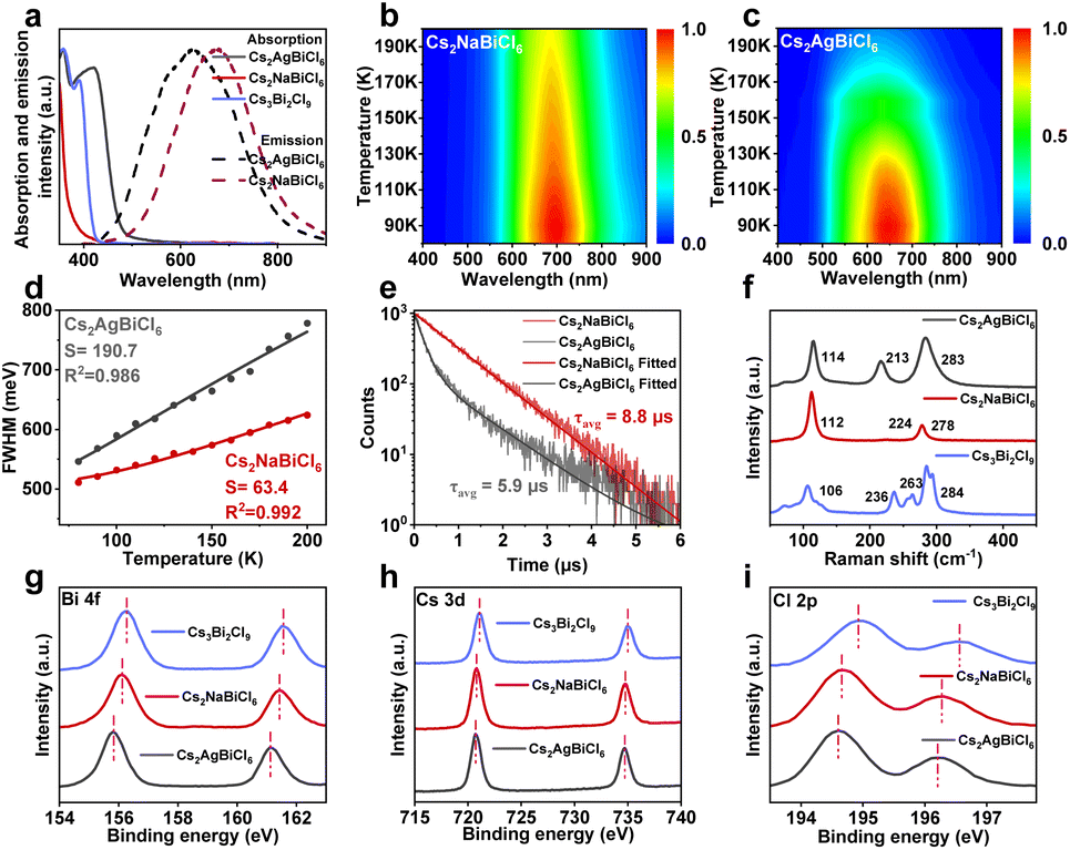 | ||
| Fig. 2 (a) Absorption and PL spectra of three bismuth-chloride perovskites. (b and c) Normalized PL spectra at varying temperatures of Cs2NaBiCl6 and Cs2AgBiCl6. (d) The FWHM as a function of temperature for Cs2NaBiCl6 and Cs2AgBiCl6. (e) PL decay curves of Cs2NaBiCl6 and Cs2AgBiCl6. (f) Raman spectra. (g–i) The X-ray photoelectron spectroscopy (XPS) spectra of Bi 4f, Cs 3d and Cl 2p (observation: the experiments described above are conducted utilizing powdered specimens). | ||
To gain more insight into the photophysical mechanisms of bismuth-chloride perovskite, temperature-dependent PL is further investigated (Fig. 2b and c). At room temperature, the emission of Cs2NaBiCl6 is barely visible. However, upon decreasing the temperature to 80 K, an emission band emerges with a peak at around 690 nm. The PL intensity continues to increase with further temperature reduction, suggesting the suppression of nonradiative recombination at lower temperatures. A similar temperature-dependent emission trend is observed for Cs2AgBiCl6. According to the characteristic PL spectra, both double perovskites exhibit STE emissions. The formation of STEs is closely associated with electron–phonon coupling effects.50 The electron–phonon coupling effect can intensively constrain the excitons and thereby restrain charge transport. Here, we investigate the effect of different monovalent ions (Ag versus Na) on the electron–phonon coupling effect. The electron–phonon coupling can be quantitatively evaluated using the Huang–Rhys factor (S), derived from the Full Width at Half Maximum (FWHM) of photoluminescence, as expressed in the following equation:51
 | (1) |
To further study the effect of lattice vibration on carrier transport, Raman spectroscopy is conducted at room temperature, using a 532 nm laser beam (Fig. 2f). Phases are observed in the range of 50 to 400 cm−1. In the orthorhombic phase of Cs3Bi2Cl9, there are two types of [BiCl6]3− polyhedra with low symmetry (Fig. S2†). The lower symmetry of the [BiCl6]3− polyhedron in the orthorhombic phase may contribute to a higher number of Raman bands, indicating more open scattering channels to enhance carrier-phonon scattering.55 Following the assignment of analogues in previous studies of Cs2AgBiCl6.56 the band at 115 cm−1 is attributed to the breathing vibration of the Ag–Cl bonds with T2g symmetry. The two bands at 212 and 284 cm−1 correspond to the stretching vibrations of the [AgCl6]5− octahedron with different vibrational symmetries of Eg and A1g, respectively. Notably, due to the stronger bonding strength of Bi–Cl compared to Na–Cl, [BiCl6]3− lattice vibrations in Cs2NaBiCl6 dominate the Raman spectra (Fig. S2†). The decreased intensity of the Eg vibration from Cs2AgBiCl6 to Cs2NaBiCl6 can be associated with the asymmetric stretching of the [BiCl6]3− octahedron. This implies that the replacement of Na ions reduces electron–phonon interaction, weakening non-radiative transitions.
To study the difference in the electronic interaction before and after monovalent ion introduction, XPS is carried out. In the XPS spectra of Cl 2p, Bi 4f, and Cs 3d (Fig. 2g–i), the binding energy for Cl 2p shifts to a lower value after the introduction of monovalent ions, indicating an increase in electron density around Cl and a feasible electron transfer from monovalent ions to Cl. The decrease in Cl 2p electron binding energy in Cs2B(I)BiCl6 is associated with the shorter B(I)–Cl bond length compared to the Bi–Cl bond in Cs3Bi2Cl9, resulting in a stronger interaction between B(I) and Cl (Fig. S2†). Additionally, a slight decrease in the binding energy of Bi 4f is observed for Cs2B(I)BiCl6 compared with Cs3Bi2Cl9, ascribed to the elimination of [BiCl6]3− octahedral distortion and an increase in the Cl–Bi–Cl bond angle (Fig. S2†), weakening the interaction between Bi and Cl. Compared with Cs3Bi2Cl9, the negative shift of Cs 3d peaks in Cs2B(I)BiCl6 is indicative of increased electron density around Cs. Overall, due to structural transformations, especially the elimination of [BiCl6]3− octahedral distortion, the binding energy of electrons around Cl, Bi, and Cs in Cs2B(I)BiCl6 is reduced to varying degrees, indicating more dispersed electronic distributions.53 Moreover, the degree of negative shift is larger in Cs2AgBiCl6 than in Cs2NaBiCl6, suggesting that the conductivity of Cs2AgBiCl6 is more outstanding than that of Cs2NaBiCl6.
To evaluate the potential in X-ray detectors, we calculate the absorption coefficient of the Cs3Bi2Cl9, Cs2AgBiCl6 and Cs2NaBiCl6 SCs as a function of photon energy utilizing the photon cross-section database. Fig. 3a illustrates that the absorption coefficient of the three bismuth-chloride perovskite SCs is significantly higher than that of Si across the entire photon energy range, and comparable to that of the inorganic semiconductors CdTe and Cs2AgBiBr6. The X-ray attenuation formula is employed to predict the X-ray stopping ability, as follows:57,58
| I = I0exp(−μmd) = I0exp(−αρd) | (2) |
 | ||
| Fig. 3 (a) Absorption coefficients of semiconductors as a function of photon energy. (b) Attenuation efficiency of 50 keV X-ray photons versus thickness. (c) Device structure of Cs2AgBiCl6 and Cs2NaBiCl6 SC detectors. (d–f) The variations among resistance, the carrier mobility-lifetime product (μτ) and the on/off ratio. (g) The sensitivity at different bias values. (h) Comparison of sensitivity among 3D, 2D and 1D bismuth-based perovskite X-ray detectors. (i) X-ray dose rate-dependent signal-to-noise ratio (SNR) at 10 V bias. (Six single crystal devices are prepared for each single crystal shown in Tables S3–S5.† The resistivity of a single crystal can be used to assess its quality. Higher resistivity is indicative of superior crystal quality, and thus, we selected the single crystal with the highest resistivity for subsequent experiments.) | ||
To achieve high sensitivity and a low detection limit in X-ray detection materials, certain prerequisites must be met, including a high μτ product, large bulk resistivity, and a high on/off ratio. To determine the bulk resistivity, I–V measurements are conducted in the dark (Fig. 3d). Cs3Bi2Cl9 has the highest resistivity, followed by Cs2NaBiCl6, and Cs2AgBiCl6. However, these values exceed that of the pristine Cs2AgBiBr6 SC (2.59 × 10⁹ Ω cm),34 indicating that chloride has a higher resistivity than bromide. Simultaneously, Cs2NaBiCl6 is not as conductive as Cs2AgBiCl6. [NaX6]5− with high ionic bonding properties in Cs2NaBiCl6 acts as an electronic barrier, increasing the resistivity of the perovskite. Additionally, the Ag+ with d10 orbitals significantly contributes to the construction of the valence band maximum (VBM), thereby improving the carrier transport. Furthermore, photoconductivity measurements were conducted, and the μτ product is determined by fitting the photoconductivity curve with the modified Hecht equation:59
 | (3) |
Sensitivity is a critical parameter of the detector and requires considerable attention. To study the sensitivity of bismuth-chloride perovskites, the data of the X-ray response are evaluated. The formula for sensitivity is expressed as the difference between photocurrent and dark current per unit dose rate and unit cross-sectional area:60
 | (4) |
To achieve high-performance X-ray detection, sensitivity is not the only crucial factor. The minimum detectable dose rate, also known as the detection limit, is equally important. To determine the detection limit, we calculated the signal-to-noise ratio (SNR) of the response current at different dose rates. The SNR as a function of dose rate is shown in Fig. 3i. According to the International Union of Pure and Applied Chemistry (IUPAC) definition, the detection limit is equal to the dose rate that can generate an average response signal larger than 3 times the signal noise. To obtain the X-ray response at lower dose rates, we use aluminum foil to block the radiation and accurately calibrated the corresponding dose rates as shown in Fig. S18.† In this work, we extended the fitting line of the dose-rate-dependent SNR to 3, determining the detection limit of the Cs2NaBiCl6 SC detector to be 59.4 nGy s−1 at a 10 V bias. This result showcases the lowest detection limit in 3D double bismuth-based perovskite.
The X-ray response of Cs2NaBiCl6 SC detectors is excellent due to their exceptional crystal quality and optoelectronic properties. Their dose-rate dependent net photocurrent densities at different bias voltages are shown in Fig. S12,† illustrating the signal current density of Cs3Bi2Cl9, Cs2AgBiCl6 and Cs2NaBiCl6 devices at different biases and dose rates.
To study the stability of the bismuth-chloride perovskites, thermogravimetric analysis (TGA) and XRD are performed. Fig. 4a shows the TGA results for the decomposition of Cs3Bi2Cl9, Cs2AgBiCl6, and Cs2NaBiCl6 SCs. Notably, Cs2NaBiCl6 exhibits a high decomposition initiation temperature of 505 °C. In comparison, Cs2AgBiBr6 and Cs3Bi2Br9 SCs begin to decompose at 430 °C and 350 °C, respectively.61 Furthermore, after 1 year under atmospheric conditions and at a temperature of 25 °C, Cs2NaBiCl6 demonstrates exceptional environmental stability, as evidenced by the consistent FWHM of the peak (220) compared to that one year ago shown in Fig. 4b. In addition, to trace the changes in the oxidation state, environment and halogen migration, fitted XPS parameters of the central metal ion and halogen have been provided before and after X-ray detection in Fig. S19.† It is established that the binding energies of the elements of bismuth chloride-based perovskite are not significantly changed before and after X-ray irradiation, suggesting that consistent chemical and physical properties were maintained after irradiation. Besides, we evaluated the trap-state density of the Cs2NaBiCl6 SCs using a space-charge-limited current (SCLC) method. It shows a ntrap of 1.20 × 1010 cm−3, which is only a 13% improvement over that of the newly made device. And μ is found to be 1.24 × 10⁻⁴ cm2 V−1 s−1, which is reduced by 23% compared to that of freshly made devices in Fig. S20.† This demonstrates that Cs2NaBiCl6 SC devices have good stability.
 | ||
| Fig. 4 (a) TGA comparison of Cs3Bi2Cl9, Cs2AgBiCl6 and Cs2NaBiCl6. (b) XRD patterns before and after ambient storage (1 year) of Cs2NaBiCl6. (c) Dark current tracking of the detector and photo response of the Cs2NaBiCl6 SC device under continuous X-ray irradiation. (d) On–off stability to X-rays at room temperature. | ||
To study the device stability, the long-term operation and a series of on–off switches are investigated. The dark current drift (Idrift) is another vital parameter of X-ray detectors, obtained by using:62
 | (5) |
Conclusions
In conclusion, we have demonstrated novel bismuth-chloride perovskites for highly sensitive and stable X-ray detection. By the introduction of monovalent metal cations, silver, and sodium, 1D Cs3Bi2Cl9 can be converted to 3D double perovskite with alternating [B(I)Cl6]5− (B = Ag, Na) and [BiCl6]3− octahedra, optimizing the optoelectronic properties and increasing the electronic dimensions. The compositional substitution strategy (Ag versus Na) allows for versatile tuning of high resistivity and high μτ, which are typically contradictory parameters for radiation detection. Besides, temperature-dependent PL as well as Raman spectroscopy robustly confirm that 3D Cs2NaBiCl6 can significantly reduce the giant electron–phonon coupling effect, which is widely present in double perovskites. The optimized 3D Cs2NaBiCl6 devices exhibit a high sensitivity of 354.5 μC Gy−1 cm−2 and a low detection limit of 59.4 nGy s−1 at an external bias of 10 V, demonstrating long-term operational stability. Our results also suggest a new direction for the design of a lead-free perovskite to realize highly sensitive X-ray detection with extreme stability, potentially stimulating further exploration of lead-free perovskites for diverse applications.Data availability
The data that support the findings of this study are available in the ESI† of this article.Author contributions
H. Chen and W. Ning conceived the idea for the manuscript and designed the experiments; H. Chen and Q. Han developed the synthesis procedures and performed the basic chemical and physical characterization; Y. Shen participated in the SC-XRD characterization; H. Qin assisted in the data analysis; W. Ning and Y. He guided the experiments, discussed the data, and led the project; H. Chen wrote the original draft and W. Ning, Y. He, Y. Wang, Y. Liu, and H. Lv reviewed and edited the draft.Conflicts of interest
There are no conflicts to declare.Acknowledgements
The authors thank Feng Gao (Linköping University, Sweden) for insightful discussions. This work was supported by the Suzhou Key Laboratory of Functional Nano & Soft Materials, the Collaborative Innovation Center of Suzhou Nano Science & Technology, the 111 Project, the Joint International Research Laboratory of Carbon-Based Functional Materials and Devices, the National Natural Science Foundation of China (22103054 and 22161132026), the Gusu Innovation and Entrepreneurship Leading Talent Program (ZXL2023188), and the Jiangsu Key Laboratory for Carbon-Based Functional Materials and Devices (Z221311). Y. H. thanks the National Key R&D Program of China (2021YFF0502600 and 2021YFB3201000), the National Natural Science Foundation of China (U2267211), the Jiangsu Natural Science Foundation (BK20210711) and the Suzhou Innovation and Entrepreneurship Leading Talent Plan Project. Y. W. thanks the National Natural Science Foundation of China (No. 52302315) and the talent project of the ZJU-Hangzhou Global Scientific and Technological Innovation Center (No. 02170000-K02013017).Notes and references
- C. Szeles, Phys. Status Solidi B, 2004, 241, 783–790 CrossRef CAS.
- H. Wei and J. Huang, Nat. Commun., 2019, 10, 1066 CrossRef PubMed.
- W. H. a. C. Brabec, Nat. Photonics, 2016, 10, 288–289 CrossRef.
- L. B. Martin Hoheisel, J. Non-Cryst. Solids, 2001, 266, 1152–1157 Search PubMed.
- V. V. Nagarkar, S. R. Miller, S. V. Tipnis, A. Lempicki, C. Brecher and H. Lingertat, Nucl. Instrum. Methods Phys. Res., Sect. B, 2004, 213, 250–254 CrossRef CAS.
- D. Pacella, Rep. Med. Imaging, 2015, 8, 1–13 Search PubMed.
- F. Cao, D. Yu, W. Ma, X. Xu, B. Cai, Y. M. Yang, S. Liu, L. He, Y. Ke, S. Lan, K.-L. Choy and H. Zeng, ACS Nano, 2020, 14, 5183–5193 CrossRef CAS PubMed.
- Y. Huang, L. Qiao, Y. Jiang, T. He, R. Long, F. Yang, L. Wang, X. Lei, M. Yuan and J. Chen, Angew. Chem., Int. Ed., 2019, 58, 17834–17842 CrossRef CAS PubMed.
- F. Yao, K. Dong, W. Ke and G. Fang, ACS Nano, 2024, 18, 6095–6110 CrossRef CAS PubMed.
- H. Huang and S. Abbaszadeh, IEEE Sens. J., 2020, 20, 1694–1704 CAS.
- S. O. Kasap, J. Phys. D: Appl. Phys., 2000, 33, 2853–2865 CrossRef CAS.
- Z. Chen, Y. Zhu and Z. He, Nucl. Instrum. Methods Phys. Res., Sect. A, 2020, 980, 164501 CrossRef CAS.
- S. Del Sordo, L. Abbene, E. Caroli, A. M. Mancini, A. Zappettini and P. Ubertini, Sensors, 2009, 9, 3491–3526 CrossRef CAS PubMed.
- S. Kasap, J. B. Frey, G. Belev, O. Tousignant, H. Mani, J. Greenspan, L. Laperriere, O. Bubon, A. Reznik, G. DeCrescenzo, K. S. Karim and J. A. Rowlands, Sensors, 2011, 11, 5112–5157 CrossRef CAS PubMed.
- S. K. Chaudhuri, K. Nguyen, R. O. Pak, L. Matei, V. Buliga, M. Groza, A. Burger and K. C. Mandal, IEEE Trans. Nucl. Sci., 2014, 61, 793–798 CAS.
- J. Zhang, G. Hodes, Z. Jin and S. F. Liu, Angew. Chem., Int. Ed., 2019, 58, 15596–15618 CrossRef CAS PubMed.
- C. H. Kang, I. Dursun, G. Liu, L. Sinatra, X. Sun, M. Kong, J. Pan, P. Maity, E.-N. Ooi, T. K. Ng, O. F. Mohammed, O. M. Bakr and B. S. Ooi, Light: Sci. Appl., 2019, 8, 94 CrossRef PubMed.
- M. Liu, M. B. Johnston and H. J. Snaith, Nature, 2013, 501, 395–398 CrossRef CAS PubMed.
- H. Yi, Science, 2017, 358, 1192–1197 CrossRef PubMed.
- H. Wei, Science, 2021, 371, 1359–1364 CrossRef PubMed.
- H. Wei, Y. Fang, P. Mulligan, W. Chuirazzi, H.-H. Fang, C. Wang, B. R. Ecker, Y. Gao, M. A. Loi, L. Cao and J. Huang, Nat. Photonics, 2016, 10, 333–339 CrossRef CAS.
- W. Wei, Z. Yang, X. Qiang, W. Haotong, F. Yanjun, W. Qi, D. Yehao, L. Tao, G. Alexei, C. Lei and H. Jinsong, Nat. Photonics, 2017, 11, 315–321 CrossRef CAS.
- Y. Song, L. Li, M. Hao, W. Bi, A. Wang, Y. Kang, H. Li, X. Li, Y. Fang, D. Yang and Q. Dong, Adv. Mater., 2021, 33, 2103078 CrossRef CAS PubMed.
- W. Wang, H. Meng, H. Qi, H. Xu, W. Du, Y. Yang, Y. Yi, S. Jing, S. Xu, F. Hong, J. Qin, J. Huang, Z. Xu, Y. Zhu, R. Xu, J. Lai, F. Xu, L. Wang and J. Zhu, Adv. Mater., 2020, 32, 2001540 CrossRef CAS PubMed.
- Y. He, W. Ke, G. C. B. Alexander, K. M. McCall, D. G. Chica, Z. Liu, I. Hadar, C. C. Stoumpos, B. W. Wessels and M. G. Kanatzidis, ACS Photonics, 2018, 5, 4132–4138 CrossRef CAS.
- Y. He, Z. Liu, K. M. McCall, W. Lin, D. Y. Chung, B. W. Wessels and M. G. Kanatzidis, Nucl. Instrum. Methods Phys. Res., Sect. A, 2019, 922, 217–221 CrossRef CAS.
- Y. He, L. Matei, H. J. Jung, K. M. McCall, M. Chen, C. C. Stoumpos, Z. Liu, J. A. Peters, D. Y. Chung, B. W. Wessels, M. R. Wasielewski, V. P. Dravid, A. Burger and M. G. Kanatzidis, Nat. Commun., 2018, 9, 1609 CrossRef PubMed.
- Y. He, M. Petryk, Z. Liu, D. G. Chica, I. Hadar, C. Leak, W. Ke, I. Spanopoulos, W. Lin, D. Y. Chung, B. W. Wessels, Z. He and M. G. Kanatzidis, Nat. Photonics, 2020, 15, 36–42 CrossRef.
- W. Ke and M. G. Kanatzidis, Nat. Commun., 2019, 10, 965 CrossRef PubMed.
- W. Ning and F. Gao, Adv. Mater., 2019, 31, e1900326 CrossRef PubMed.
- W. Ning, F. Wang, B. Wu, J. Lu, Z. Yan, X. Liu, Y. Tao, J.-M. Liu, W. Huang, M. Fahlman, L. Hultman, T. C. Sum and F. Gao, Adv. Mater., 2018, 30, 1706246 CrossRef PubMed.
- J. Yang, C. Bao, W. Ning, B. Wu, F. Ji, Z. Yan, Y. Tao, J. M. Liu, T. C. Sum, S. Bai, J. Wang, W. Huang, W. Zhang and F. Gao, Adv. Opt. Mater., 2019, 7, 1801732 CrossRef.
- K. Dong, H. Zhou, W. Shao, Z. Gao, F. Yao, M. Xiao, J. Li, Y. Liu, S. Wang, S. Zhou, H. Cui, M. Qin, X. Lu, C. Tao, W. Ke and G. Fang, ACS Nano, 2023, 17, 1495–1504 CrossRef CAS PubMed.
- W. Pan, H. Wu, J. Luo, Z. Deng, C. Ge, C. Chen, X. Jiang, W.-J. Yin, G. Niu, L. Zhu, L. Yin, Y. Zhou, Q. Xie, X. Ke, M. Sui and J. Tang, Nat. Photonics, 2017, 11, 726–732 CrossRef CAS.
- W. Yuan, G. Niu, Y. Xian, H. Wu, H. Wang, H. Yin, P. Liu, W. Li and J. Fan, Adv. Funct. Mater., 2019, 29, 1900234 CrossRef.
- X. Zhang, T. Zhu, C. Ji, Y. Yao and J. Luo, J. Am. Chem. Soc., 2021, 143, 20802–20810 CrossRef CAS PubMed.
- R. Zhuang, X. Wang, W. Ma, Y. Wu, X. Chen, L. Tang, H. Zhu, J. Liu, L. Wu, W. Zhou, X. Liu and Y. Yang, Nat. Photonics, 2019, 13, 602–608 CrossRef CAS.
- Y. Zhang, Y. Liu, Z. Xu, H. Ye, Z. Yang, J. You, M. Liu, Y. He, M. G. Kanatzidis and S. F. Liu, Nat. Commun., 2020, 11, 2304–2315 CrossRef CAS PubMed.
- C. Ma, H. Li, M. Chen, Y. Liu, K. Zhao and S. Liu, Adv. Funct. Mater., 2022, 32, 2202160 CrossRef CAS.
- Y. He, I. Hadar and M. G. Kanatzidis, Nat. Photonics, 2021, 16, 14–26 CrossRef.
- M. Xia, J. H. Yuan, G. Niu, X. Du, L. Yin, W. Pan, J. Luo, Z. Li, H. Zhao, K. H. Xue, X. Miao and J. Tang, Adv. Funct. Mater., 2020, 30, 1910648 CrossRef CAS.
- Y. He, C. C. Stoumpos, I. Hadar, Z. Luo, K. M. McCall, Z. Liu, D. Y. Chung, B. W. Wessels and M. G. Kanatzidis, J. Am. Chem. Soc., 2021, 143, 2068–2077 CrossRef CAS PubMed.
- A. H. Slavney, T. Hu, A. M. Lindenberg and H. I. Karunadasa, J. Am. Chem. Soc., 2016, 138, 2138–2141 CrossRef CAS PubMed.
- S. Attique, N. Ali, S. Ali, R. Khatoon, N. Li, A. Khesro, S. Rauf, S. Yang and H. Wu, Adv. Sci., 2020, 7, 1903143 CrossRef CAS PubMed.
- S. Dan, A. Maiti, S. Chatterjee and A. J. Pal, J. Phys.: Condens. Matter, 2021, 33, 485701 CrossRef CAS PubMed.
- T. Luo and J. Wei, Mater. Chem. Phys., 2020, 253, 123374 CrossRef CAS.
- S. Yirong, M. Wenbo and Y. Yang, J. Semicond., 2020, 41, 051204 CrossRef.
- K. M. McCall, C. C. Stoumpos, S. S. Kostina, M. G. Kanatzidis and B. W. Wessels, Chem. Mater., 2017, 29, 4129–4145 CrossRef CAS.
- F. Jiang, Z. Wu, M. Lu, Y. Gao, X. Li, X. Bai, Y. Ji and Y. Zhang, Adv. Mater., 2023, 35, 2211088 CrossRef CAS PubMed.
- C. Zhu, J. Jin, Z. Wang, Z. Xu, M. C. Folgueras, Y. Jiang, C. B. Uzundal, H. K. D. Le, F. Wang, X. Zheng and P. Yang, Science, 2024, 383, 86–93 CrossRef CAS PubMed.
- S. Li, J. Luo, J. Liu and J. Tang, J. Phys. Chem. Lett., 2019, 10, 1999–2007 CrossRef CAS PubMed.
- J. A. Steele, P. Puech, M. Keshavarz, R. Yang, S. Banerjee, E. Debroye, C. W. Kim, H. Yuan, N. H. Heo, J. Vanacken, A. Walsh, J. Hofkens and M. B. J. Roeffaers, ACS Nano, 2018, 12, 8081–8090 CrossRef CAS PubMed.
- L. Wan, R. Zhang, E. Cho, H. Li, V. Coropceanu, J.-L. Brédas and F. Gao, Nat. Photonics, 2023, 17, 649–655 CrossRef CAS.
- M. Shi, G. Li, W. Tian, S. Jin, X. Tao, Y. Jiang, E. A. Pidko, R. Li and C. Li, Adv. Mater., 2020, 32, 2002137 CrossRef CAS PubMed.
- J. Jiang, G. Niu, L. Sui, X. Wang, Y. Zhang, L. Che, G. Wu, K. Yuan and X. Yang, J. Phys. Chem. Lett., 2021, 12, 7285–7292 CrossRef CAS PubMed.
- Y. Pei, D. Tu, C. Li, S. Han, Z. Xie, F. Wen, L. Wang and X. Chen, Angew. Chem., Int. Ed., 2022, 61, e202205276 CrossRef CAS PubMed.
- J. Liu, B. Shabbir, C. Wang, T. Wan, Q. Ou, P. Yu, A. Tadich, X. Jiao, D. Chu, D. Qi, D. Li, R. Kan, Y. Huang, Y. Dong, J. Jasieniak, Y. Zhang and Q. Bao, Adv. Mater., 2019, 31, 1901644 CrossRef PubMed.
- F. Maddalena, L. Tjahjana, A. Xie, Arramel, S. Zeng, H. Wang, P. Coquet, W. Drozdowski, C. Dujardin, C. Dang and M. Birowosuto, Crystals, 2019, 9, 88 CrossRef.
- C. C. Stoumpos, C. D. Malliakas, J. A. Peters, Z. Liu, M. Sebastian, J. Im, T. C. Chasapis, A. C. Wibowo, D. Y. Chung, A. J. Freeman, B. W. Wessels and M. G. Kanatzidis, Cryst. Growth Des., 2013, 13, 2722–2727 CrossRef CAS.
- Y. Liu, Y. Zhang, X. Zhu, J. Feng, I. Spanopoulos, W. Ke, Y. He, X. Ren, Z. Yang, F. Xiao, K. Zhao, M. Kanatzidis and S. F. Liu, Adv. Mater., 2021, 33, e2006010 CrossRef PubMed.
- X. Li, P. Zhang, Y. Hua, F. Cui, X. Sun, L. Liu, Y. Bi, Z. Yue, G. Zhang and X. Tao, ACS Appl. Mater. Interfaces, 2022, 14, 9340–9351 CrossRef CAS PubMed.
- S. You, Z. K. Zhu, S. Dai, J. Wu, Q. Guan, T. Zhu, P. Yu, C. Chen, Q. Chen and J. Luo, Adv. Funct. Mater., 2023, 33, 2303523 CrossRef CAS.
Footnote |
| † Electronic supplementary information (ESI) available. See DOI: https://doi.org/10.1039/d5sc00061k |
| This journal is © The Royal Society of Chemistry 2025 |