DOI:
10.1039/D5RA04190B
(Paper)
RSC Adv., 2025,
15, 25187-25201
NO2 and SO2 adsorption and sensing on Janus B2SeTe: unveiling its electronic, optical, and magnetic properties through DFT and COMSOL†
Received
13th June 2025
, Accepted 2nd July 2025
First published on 16th July 2025
Abstract
In this study, the electronic, optical, and magnetic characteristics of a two-dimensional Janus B2SeTe monolayer, along with its potential for gas sensing applications, were examined using DFT and COMSOL simulations. The interaction and sensing capabilities of various gas molecules, including CO, CO2, NH3, SO2, H2S, HCN, CH4, and NO2, on the B2SeTe surface were systematically analyzed. Upon geometric optimization, a substantial enhancement in conductivity was observed, increasing by factors of 3.44 × 10¹³ and 2.44 × 10⁷ upon NO2 and SO2 adsorption, respectively. The pristine B2SeTe monolayer demonstrated remarkable sensitivity and selectivity toward NO2 and SO2, with NO2 showing a notably longer recovery time of 7.2798 × 10⁻⁴ s, indicating strong and stable adsorption. The sensor device exhibited an increased response across a concentration range of 25 ppm to 300 ppm, with higher sensitivity to NO2 (0.02068 ppm−1) compared to SO2 (0.00953 ppm−1). Furthermore, B2SeTe displayed optical sensitivity to NO2, and the observed spin splitting under NO2 adsorption revealed its magnetic sensing capability. These findings suggest that the Janus B2SeTe monolayer holds significant promise for future gas sensing applications and environmental monitoring systems.
1. Introduction
Carbon monoxide (CO), sulfur dioxide (SO2), methane (CH4), ammonia (NH3), hydrogen sulfide (H2S), carbon dioxide (CO2), hydrogen cyanide (HCN), and nitrogen dioxide (NO2) are examples of anthropogenic noxious gaseous chemicals that represent significant environmental pollution and health hazards.1 These gases are primarily released by industrial processes, the burning of fossil fuels, waste decomposition, automobile exhausts, and agricultural activities. Many of them can cause neurological, cardiovascular, and pulmonary issues, even at low doses. Moreover, being strong greenhouse gases, CH4, CO2, and NO2 all contribute to global warming.2,3 Furthermore, the ever-increasing emissions caused by the exponential growth of industry pose a threat to all forms of life on Earth.4 Worldwide, 4.2 million people die early each year as a result of outdoor air pollution, which frequently contains harmful chemicals, according to the World Health Organization (WHO). As a result, there is a need for substantial action to identify and separate these dangerous gases.5,6 Thus, accidents, occupational sickness, and environmental damage can be prevented with superior, sensitive, and cost-effective toxic-gas-sensing devices.7 In the last 10 years, many very sensitive, low-power 2D (two-dimensional) sensors have been developed.8 In addition, the unique mechanical, optical, electrical, and magnetic properties of 2D nanomaterials make them stand out among gas sensor materials.9,10 Since the discovery of graphene, the field of 2D nanomaterials has advanced tremendously.11 In the process of materials going from three-dimensional to two-dimensional, numerous scientists have studied a wide range of intriguing physical phenomena.12 Gas sensing comprises identifying and quantifying specific gases in the environment; 2D materials are well-suited for this task because of their unique properties and huge surface area.13 However, graphene's inherent metallic properties reduce the gas sensor's response sensitivity.1 For superior performance in gas sensors, 2D layered materials with semiconducting properties are required.14,15 The transport characteristics of semiconductor 2D layers with tunable electronic properties can be altered by light or gate bias, which makes them very attractive for enhancing sensing capabilities.16 Transition metal dichalcogenides (TMDs) have excellent properties, such as large band gaps, high carrier mobility, and high surface-to-volume ratios, as well as a hexagonal honeycomb structure, which make them an attractive alternative to graphene.6,17
Recently, TMDs have garnered a lot of interest and are regarded as suitable alternative materials to graphene owing to their fascinating physical and chemical properties, including topological superconductivity, high surface area, abundant active sites, layer-dependent tunable bandgap, chemical stability, indirect-to-direct bandgap crossover, valley-selective optical stimulation, out-of-plane piezoelectric polarization, and a significant Rashba effect because of their out-of-plane asymmetry.15,17,18 In particular, the 2D Janus TMDs, such as MoSSe, WSSe, FeClF, MnSSe, PtSSe, In2SSe, Ga2SSe, WSTe, HfSeTe, PdSSe, are promising for gas sensing devices.19–23 Kumar et al.24 utilized a first-principles approach based on density functional theory (DFT) to examine the structural, electronic, and mechanical properties of two-dimensional Janus group III ternary chalcogenide monolayers, including B2XY, Al2XY, and BAlX2, where X and Y represent S, Se, or Te. Among the various Janus TMDs, MoSSe has been successfully synthesized through the chemical vapor deposition (CVD) method.25,26 Jin et al. reported that Janus MoSSe exhibits significantly enhanced sensitivity to NH3 and NO2 gases, attributing this improvement to the built-in electric field and tunable selectivity enabled by its asymmetric Janus structure, making it a promising candidate for ultra-high-sensitivity nanoscale gas sensors.27 Similarly, Kaur et al. demonstrated the use of Substituted 2D Janus WSSe monolayers as an efficient nanosensor for CO, NO, and HF gas sensing without imposing external strain.28 More recently, a novel 2D Janus boron selenium telluride monolayer, B2SeTe, featuring asymmetric Se/Te surfaces, was introduced with superior structural, electronic, photocatalytic, and intrinsic dipole properties.29 Qiu et al. investigated the piezoelectric properties of the Janus B2SeTe monolayer and found that its pronounced out-of-plane piezoelectric response makes it a promising material for applications in top/bottom piezoelectric device technologies.30 However, gas adsorption on B2SeTe monolayers remains unexplored.
This work investigates the adsorption behaviour and sensing capabilities of various gases on a Janus B2SeTe monolayer. Using DFT, the study explores the electronic, optical, and magnetic properties of Janus B2SeTe, including adsorption distances, energies, structural stability, charge transfer, bandgap modulation, electrical conductivity, absorption coefficient, refractive index, and magnetic moment in the presence of different gas molecules. Additionally, NO2 and SO2 gas sensors based on Janus B2SeTe were designed and simulated using COMSOL Multiphysics, incorporating an interdigitated electrode (IDE) configuration. The simulation results demonstrate the high sensitivity and selectivity of the sensors toward NO2 and SO2 compared to other gases. These findings highlight the potential of Janus B2SeTe as a promising material for advanced gas sensing applications.
2. Methodology
2.1 Computational methods based on DFT
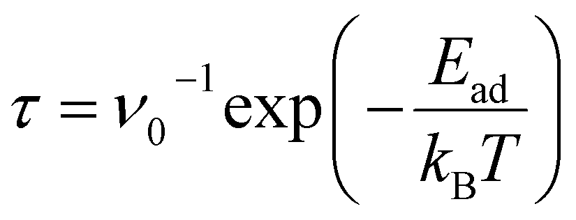
First-principles calculations based on DFT were used to compute the electrical and structural relaxations using the CASTEP tool.31 To understand the interplay of exchange correlations, the generalized gradient approximation (GGA) with the Perdew–Burke–Ernzerhof (PBE) functional and GGA-PBE + SOC were employed.10 At Grimme's suggestion, the DFT-D3 approach was used to characterize the van der Waals interaction between the gas molecules and the group III dichalcogenide monolayers.32 A 3 × 3 × 1 supercell of the monolayer B2SeTe was used in the computational model, which included gas molecules adsorbed on every surface.33 A kinetic energy threshold of 520 eV was set, and the total energy that converged was required to meet a tolerance of 10−6 eV. The electrical characteristics are computed using the 4 × 4 × 1 Monkhorst–Pack k-point mesh.34 To determine the optical characteristics and projected density of state (PDOS), the formula 8 × 8 × 1 is utilized. The geometric optimization was carried out using the Broyden–Fletcher–Goldfarb–Shanno (BFGS) algorithm.35 The following variables were initialized: the energy convergence criterion is 1.0 × 10⁻⁶ eV per atom, the force maximum is 0.01 eV Å, the stress maximum is 0.02 GPa, the displacement maximum is 5.0 × 10⁻⁴ Å, and the frequency of iterations is 100.36 To ensure optimal performance for both hard compressibility and variable cell parameters, the cell was optimized with a fixed basis quality. The Koelling–Harmon relativistic method was used for computing the electronic properties, whereas the norm-conserving method was employed for pseudopotentials. Using the GGA and GGA + SOC methods, the electronic properties of NO2 and NH3 were calculated, revealing that the splitting of energy bands is caused by the interplay of angular momentum and orbital angular momentum.37 The adsorption energy was calculated using eqn (1).25| | |
Ead = E(B2SeTe+gas) − E(B2SeTe) − E(gas)
| (1) |
The energy of the B2SeTe monolayer following gas adsorption is denoted by E(B2SeTe+gas), the energy of the B2SeTe monolayer itself is denoted by E(B2SeTe), and the total energy of the sole gas layer is denoted by E(gas). Eqn (2) was used to determine the amount of charge transfer during the adsorption phase, where ρtotal, ρm, and ρgas represent the total charge density of the adsorbed structure, the charge density of the pristine molecule, and the charge density of the gas molecule, respectively.
| | |
Δρ = ρ(total) − ρm − ρgas
| (2) |
The charge transfer amount in the adsorption process was calculated using eqn (3):
where
Qiso and
Qads indicate the total charge of the gas molecule before and after adsorption, respectively. The conductivity from the band gap of a material can be found in the following equation:
10| |
 | (4) |
Here,
A is the proportionality constant,
Eg is the band gap,
KB is the Boltzmann constant, and
T is the temperature. The relationship between chemiresistive sensitivity and conductivity is defined by
eqn (5):
13| |
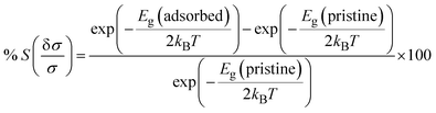 | (5) |
where
Eg(adsorbed) represents the band gap after gas adsorption on B
2SeTe, and
Eg(pristine) represents the band gap of pristine B
2SeTe. The duration necessary for gas molecules to naturally desorb from the surface of the sensing material is referred to as the recovery period. The recovery duration was determined with the Van't Hoff–Arrhenius equation, as presented below:
10,38,39| |
 | (6) |
Here, the attempt frequency is denoted as
ν0. Previous studies have found that 10
12 s
−1 is the attempt frequency for SO
2. For all other gases, the same value can be applied.
13
Gas molecules were subsequently added to the initial adsorption sites to determine the most stable adsorption site. The five chosen adsorption sites: B (top of B atom), Se (top of Se atom), Te (top of the centre of the hexagon), bridge (top of B–Se bonds), and bridge (top of B–Te bonds), are shown in Fig. 1(a). The bond length and angle of the 2D layered Janus structure of B2SeTe can be seen in Fig. 1(b). The sandwich structure best describes these structures, which exhibit P3m1(C3V) symmetry. Within the B2SeTe monolayer, the unit cell's lattice constants are a = b = 4.075 Å. These lattice parameters match the earlier research on this substance. An example of a unit cell in Fig. 1(a) is marked by the red rhombus box. This cell contains a four-atom basis lattice, with one selenium (Se) atom, two metallic boron atoms, and one tellurium (Te) atom. Fig. 1(b), in its side view, shows the Z-axis order of covalently bound atomic layers as Se–B–B–S, suggesting that boron is sandwiched between selenium (Se) and tellurium (Te) atoms.
 |
| | Fig. 1 The optimized structure of the B2SeTe monolayer showing the (a) five adsorption sites and (b) optimized parameters. | |
2.2 Computational methods on COMSOL
The sensor is built on a 1 × 2 × 0.1 mm3 alumina (Al2O3) substrate and comprises four main components: the sensing layers, the IDE, the heater, and the substrate itself, as shown in Fig. S1(a).†40,41 The B2SeTe monolayer on top of IDEs acts as a sensing layer, and the bottom electrodes serve as heaters.42,43 The thickness of the B2SeTe layer was set to 0.5 μm, with a surface area of 950 × 1700 μm2 to represent a realistic device-scale geometry. On the rear face of the Al2O3 substrate, an 800 × 500 μm2 patch of RuO2 acts as a resistive heater, allowing the sensor's temperature to be modulated (including operation at room temperature) by adjusting the bottom-electrode voltage within COMSOL Multiphysics.44 The entire assembly sits inside a sealed, cylindrical test chamber (4 mm in diameter and height) equipped with one inlet and two 0.35 mm radius outlets, as shown in Fig. S1(b).† During the gas sensing experiments, the target gas is introduced through the inlet and exits via the outlets; flow-induced pressure causes the thin sensor membrane to flex slightly. As the gas travels from the inlet to the outlet, its concentration decreases progressively.40,45 Various amounts of gas were injected into the chamber through the inlet and exposed to the sensor surface during the simulation.46 The chamber was emptied of any remaining gas before each measurement. The researchers in this work utilized COMSOL Multiphysics to resolve PDEs and the physical interactions that go along with them. With COMSOL Multiphysics, you can access several modules.47
The Navier–Stokes equation is employed to describe the gas flow within the chamber.48
where
P,
ρ,
η,
U, and
g represent gas pressure, gas flux, viscosity, velocity field, and gravity, respectively. To determine the gas's velocity and field, the Navier–Stokes equations must be solved with the equation of continuity:
48,49
Given the incompressibility of gas flow, where ρ remains constant, the equation can be written as:
The gas chamber walls are in a no-relative-motion situation, with UT standing for the peripheral velocity.
According to Fourier's rule, a material's heat transfer rate is proportional to the negative gradient of its temperature.
Here,
T,
q′′, and
k represent the temperature, flux density, and thermal conductivity, respectively. The conductivity,
σ, can be expressed as:
Where the charge, carrier concentration, and mobility are represented by
e,
n, and
μ, respectively. The sensor conductivity upon the exposure of a target gas at concentration
C can be expressed as:
50,51where
α is the adsorption coefficient, and
t represents the per unit surface area of the active layer. This equation can be modified to:
| | |
Sensor response = Ra/Rg
| (15) |
where
Rg and
Ra stand for the sensing layer's resistance in the presence of gas and air, respectively.
3. Results and discussion
3.1 The electronic and structural properties of Janus B2SeTe monolayer
The pristine B2SeTe Janus structure was first developed and examined for structural stability. Fig. 1 shows that for the pristine B2SeTe structure, the bond lengths of B–Se (d1), B–B (d2), and B–Te (d3) are 2.153 Å, 1.683 Å, and 2.129 Å, respectively, and the angles of B–B–Se (θ1), B–B–Te (θ2), B–Se–B(θ3) and B–Te–B (θ4) are 114.329°, 117.871°,104.215°, and 99.914°, respectively, and the effective thickness of the B2SeTe structure (t) is 4.9 Å.
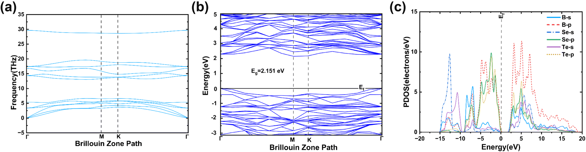
Fig. 2 shows the phonon dispersion, electronic band structures, and PDOS of the B2SeTe monolayer. The phonon dispersion shows no imaginary frequencies, indicating that the structure is dynamically stable (Fig. 2(a)). The phonon band dispersion of the B2SeTe structure shows a total of 12 phonon branches. Three of these branches are acoustic, while the other nine are optical, consistent with theoretical conclusions.35 Even at the high-symmetry locations close to the zone boundary, the gap in the phonon dispersion separates the degenerate and non-degenerate branches. In addition, the acoustic branches are scattered linearly close to the Gamma point, which is consistent with the typical characteristics of two-dimensional monolayers, matching previous research.24 Fig. 2(b) shows the electrical band structure of the pristine B2SeTe monolayer. The calculated GGA-PBE bandgap is 2.151 eV, consistent with previous research.29,30 The band gap formation occurs between the Γ-high-symmetry point in the valence band maximum (VBM) and the M-high point in the conduction band minimum (CBM). Fig. 2(c) demonstrates that the Se-p and B-p orbitals contribute most to the VBM while the B-p orbital contributes most to the CBM, based on the PDOS. Table S I† integrates all structural property data for the Janus monolayer, including the work function, bandgap value, and associated positions of the VBM and CBM.
 |
| | Fig. 2 (a) The phonon dispersion, (b) band structure, and (c) PDOS of the pristine B2SeTe monolayer with a band gap of 2.151 eV. | |
3.2 Gas adsorption behaviour on Janus B2SeTe monolayer
Fig. 3 shows the top view and side view of the most energetically favourable adsorption configurations for (a) NH3, (b) HCN, (c) CO, (d) NO2, (e) CH4, (f) SO2, (g) H2S, and (h) CO2 gas molecules on the B2SeTe monolayer. Additionally, the orientations of the gas molecules are also different. The charge transfer and adsorption energy are assessed to determine the adsorption properties. A chemisorption process generally requires an adsorption energy of −0.5 eV or less (higher in absolute value).10,35 The subsequent section addresses the adsorption configurations and the characteristics of gas molecule adsorption.
 |
| | Fig. 3 Top and side view of the most energetically favourable adsorption configuration of (a) NH3, (b) HCN, (c) CO, (d) NO2, (e) CH4, (f) SO2, (g) H2S, and (h) CO2 gas molecules on the B2SeTe monolayer. | |
3.2.1 NH3. The B2SeTe monolayer showed inefficient NH3 adsorption with an energy of −0.218 eV. According to Fig. 3(a), the optimal location for adsorption was on top of the Te atom. The adsorption distance between the B2SeTe monolayer and the NH3 gas molecule was determined to be 3.11 Å. There was no impact on the conductivity as a chemiresistive gas sensor for NH3 detection due to the insignificant change in band gap of about 0.002 eV. With a charge transfer of −0.053e, charge was transferred from the B2SeTe monolayer to NH3, indicating that NH3 served a charge acceptor due to the negative sign. As shown by the significant charge depletion on the Se and B atoms in Fig. 4(a), charge was depleted on the H atoms and accumulated on the Se atoms, with a modest buildup on the N atom. Because of the long distance, low adsorption energy, and charge transfer, NH3 was physisorbed on the B2SeTe monolayer.
 |
| | Fig. 4 Charge density difference (CDD) plots for (a) NH3, (b) HCN, (c) CO, (d) NO2, (e) CH4, (f) SO2, (g) H2S, and (h) CO2 adsorbed on the B2SeTe monolayer. The blue (yellow) signifies electron accumulation (depletion). The isovalue is 0.001 electrons per unit Å3. | |
3.2.2 NO2. The B2SeTe monolayer's predicted adsorption energy for NO2 is −0.528 eV, indicating a highly energetically favourable adsorption mechanism. The apex of the B–Se bond was found to be the ideal adsorption location, as shown in Fig. 3(d). With a surface-to-molecule distance of 2.51 Å, the measured adsorption distances for N–Se and N–B bonds were roughly 2.805 Å and 4.078 Å, respectively. Out of all the gas molecules, NO2 had the shortest adsorption distance. After NO2 gas adsorption, a notable band gap change of −0.163 eV was produced, suggesting that the B2SeTe monolayer is extremely sensitive and selective for NO2 gas molecules. From the B2SeTe to the NO2 gas molecule, the Hirshfeld charge transfer is −0.087e. The large charge deposited on the N atom, as seen in Fig. 4(d), and the significant charge depletion on the Se and B atoms further supports the negative sign, which indicates that NO2 acts as a charge acceptor. The NO2 molecule appears to be chemisorbed on the B2SeTe monolayer based on the substantial adsorption energy, low adsorption distance, and charge transfer.
3.2.3 SO2. Adsorption of SO2 onto the B2SeTe monolayer was found to have an energetically unfavourable adsorption energy of −0.13 eV. Fig. 3(f) shows that the best place for adsorption was at the very top of the B–Se bond. The effective longitudinal adsorption distance was 3.273 Å, and the distances for S–Se and S–B bonds were around 3.37 Å and 4.701 Å, respectively. According to the calculations, the Hirshfeld charge transfer from B2SeTe to SO2 gas is −0.099e, which was the largest among all gas molecules. The negative sign and the substantial charge depletion on the Se and B atoms and a considerable accumulation on the S atom (Fig. 4(f)) show that SO2 is a charge acceptor. The substantial charge transfer, low adsorption energy, and medium adsorption distance support the physisorption of SO2 on the B2SeTe monolayer.
3.2.4 HCN. The adsorption energy of HCN on the B2SeTe monolayer is notably low at −0.1 eV. Fig. 3(b) indicates that the top of the Se atom functioned as the optimal adsorption site, with a total adsorption distance of 3.35 Å. The B2SeTe and HCN gas molecules exhibit a Hirshfeld charge transfer of −0.057e. A negative sign signifies that HCN acts as a charge acceptor, and Fig. 4(b) illustrates considerable charge depletion in the Se and B atoms. Some charge is also accumulated on the H atoms and Se atoms indicated in blue. The low adsorption energy, considerable adsorption distance, and charge transfer suggest that the HCN gas molecule is physically adsorbed onto the B2SeTe monolayer.
3.2.5 H2S. The adsorption energy calculated for H2S was about −0.1 eV. As shown in Fig. 3(g), the B atom's top surface was the most favourable location for adsorption. The adsorption distance between the upper surface and the gas molecule was 3.05 Å. The estimated Hirshfeld charge transfer from a B2SeTe molecule to a H2S gas molecule is −0.06e, which can be identified in Fig. 4(g). There was considerable charge accumulation on S atoms with charge depletion on the Se atoms. However, according to the results in Fig. 5(d), a notable shift of 0.015 eV in the band gap was seen upon H2S adsorption on the B2SeTe monolayer. The presence of charge transfer, low adsorption energy, and high adsorption distance suggests that the H2S molecule is physisorbed onto the B2SeTe monolayer.
 |
| | Fig. 5 The band structures of (a) the pristine B2SeTe monolayer and the B2SeTe monolayer with (b) CH4, (c) CO2, (d) H2S, (e) SO2, (f) NO2, (g) CO, (h) HCN, and (i) NH3 adsorbed. The blue (red) color indicates up (down) spin. | |
3.2.6 CO2. A very weak and steady adsorption of CO2 was determined to occur on the B2SeTe monolayer, with an adsorption energy of −0.015 eV. As seen in Fig. 3(h), the preferred adsorption site was the top of the B atom. CO2 adsorbs on the monolayer surface with an effective adsorption distance of 3.07 Å. Between the B2SeTe and CO2 gas molecules, the estimated Hirshfeld charge transfer is −0.049e. The charge transfer is evident from the charge depletion observed on the B2SeTe monolayer surface and the charge accumulation on the CO2 molecule, as illustrated in Fig. 4(h). The negative sign denotes that CO2 functions as a charge acceptor. The CO2 molecule appears to be physically adsorbed on the B2SeTe monolayer, as evidenced by the low adsorption energy, high adsorption distance, and charge transfer.
3.2.7 CO. Adsorption of CO onto the B2SeTe monolayer was found to have an energy of −0.017 eV, suggesting very weak and persistent adsorption. As seen in Fig. 3(c), the preferred adsorption site was the top of the Te atom. CO adsorbs with the largest adsorption distance of 3.98 Å on the B2SeTe monolayer. According to the calculations, the Hirshfeld charge transfer from B2SeTe to CO gas is −0.009e, which was the lowest among all the gas molecules. No charge piling between the CO molecule and the B2SeTe monolayer was observed, as shown in Fig. 4(c). When CO comes close to the surface, not enough interaction takes place between the CO and the B2SeTe monolayer. Characteristics such as limited charge transfer, long adsorption distance, and low adsorption energy suggest that the CO molecule is physically adsorbed onto the B2SeTe monolayer.
3.2.8 CH4. The adsorption energy of CH4 on the B2SeTe monolayer was −0.002 eV, signifying poor and stable adsorption. Fig. 3(e) illustrates that the higher Se atom was the favoured adsorption site, with the adsorption distance measured at 3.04 Å. Nevertheless, upon the adsorption of CH4 onto the B2SeTe monolayer, the band gap exhibited a notable alteration of 0.003 eV, as illustrated in Fig. 5(b). The predicted Hirshfeld transfer involves transferring −0.023e of charge from B2SeTe to CH4 gas. The charge transfer is manifested in the charge depletion noted on the B2SeTe monolayer surface and the charge accumulation on the CH4 molecule, as depicted in Fig. 4(e). The charge is predominantly concentrated on the carbon atom and the lower hydrogen atom. The low adsorption energy, significant adsorption distance, and charge transfer indicate that CH4 is physisorbed on the B2SeTe monolayer.
3.3 Electronic structures and atomic contributions after gas adsorption
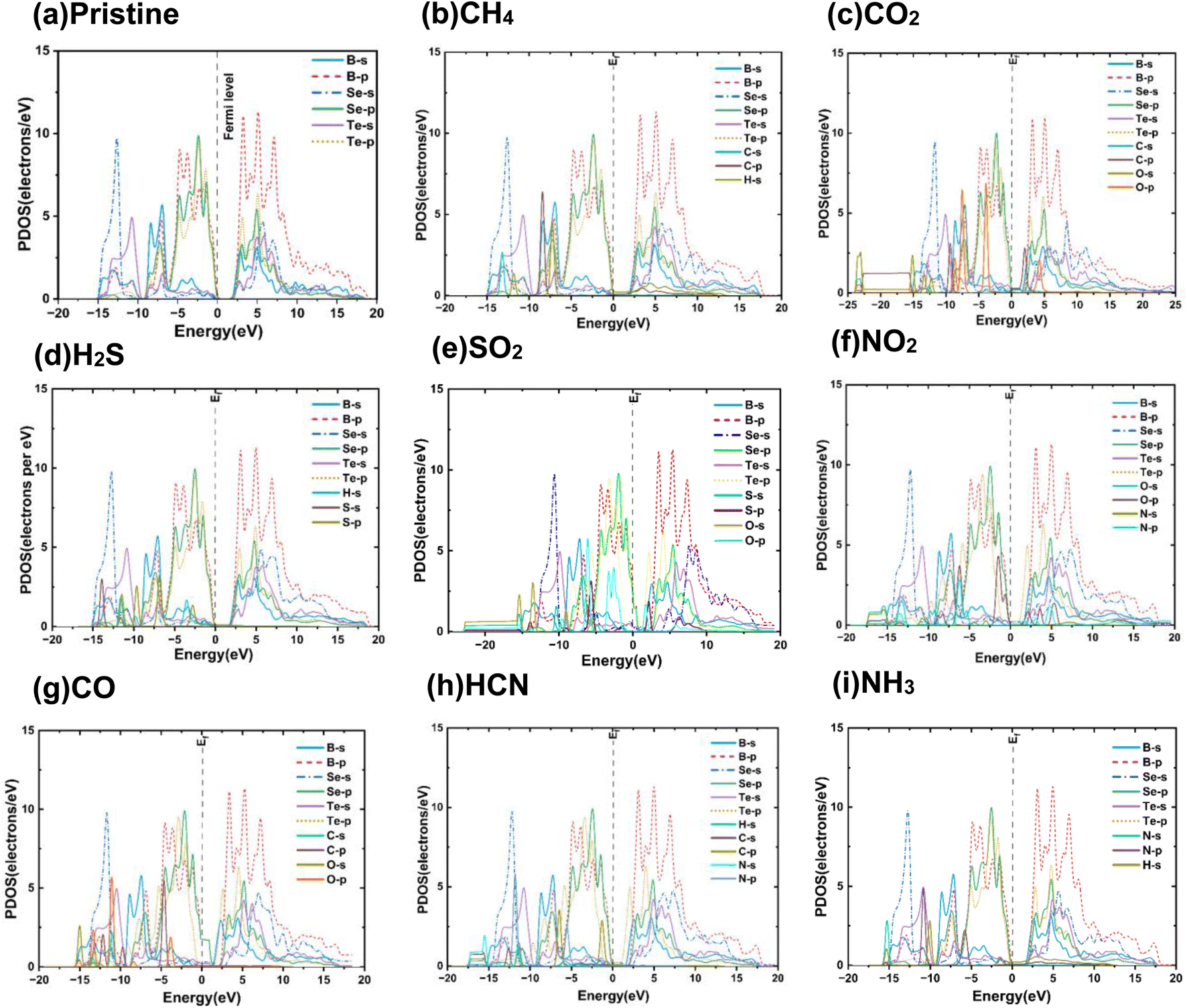
The presence of gas molecules is anticipated to modify the electronic structures of the B2SeTe monolayer. Consequently, the orbital PDOSs and band structures were computed. Fig. 5 shows the band structures of all gas-adsorbed systems. Fig. 5(b) and (i) demonstrates that the impact of CH4 and NH3 on the electronic properties of the B2SeTe monolayer is negligible. The observed change in the band gap was insignificant. The nitrogen and hydrogen atoms in NH3 and CH4 molecules contribute negligibly to the DOS, as depicted in Fig. 6(b) and (i). B-p and Se-p orbitals contribute most to the conduction band (CB) and valence band (VB), respectively, the same as for the pristine B2SeTe. The adsorption of SO2 altered the electronic structure of the B2SeTe monolayer, leading to a decreased band gap of 1.295 eV, as depicted in Fig. 5(e). A significant hybridization among the p orbitals of Se, O, and S atoms was observed in the CB in the range of 1 eV to 2 eV, as shown in Fig. 6(e). This hybridization may have caused a shift in the CB, perhaps altering the band gap. A new state occurs, mainly due to the contribution of O-p orbitals both in CB and VB. The substantial hybridization also occurred when NO2 was adsorbed onto B2SeTe. In this case, hybridization occurred between the p orbitals of nitrogen and selenium atoms. The adsorption of NO2 led to the formation of new states, as depicted in Fig. 6(f). Incorporating extra states within the 0.5 to 1.5 eV range led to a notable decrease in the band gap to 0.538 eV following NO2 adsorption, as depicted in Fig. 5(f). Furthermore, substantial hybridization between the orbitals of NO2 and B2SeTe was observed. Fig. 6(f) demonstrates that the p orbitals of N atom hybridize with the s and p orbitals of boron and selenium in the 0.5 to 2 eV range. The p orbitals of O atoms hybridize with the p orbitals of Se atoms, exhibiting energy levels between −0.5 and −1.5 eV in the VB. The changes in the band gap were primarily caused by the O-p orbitals. Additionally, a large band gap change leads to a change in conductivity. A significant amount of variation in the conductivity of the B2SeTe monolayer is responsible for the sensitivity of the material. This makes it suitable for application as a chemiresistive gas sensor. In contrast, H2S adsorption did not alter the electronic structure of the B2SeTe monolayer. However, weak hybridization between the sulfur and boron atoms is observed in the 2 to 4 eV range within the VB, as depicted in Fig. 6(d). The change in the band gap was negligible (0.09 eV), as depicted in Fig. 5(d). The HCN adsorption modified the electronic structure of the B2SeTe monolayer. Fig. 6(h) demonstrates that the p orbitals of the carbon atom in the HCN molecule undergo substantial hybridization with the p orbitals of the boron atom throughout the 1.8 eV to 2.2 eV range of the CB. S-p orbitals contribute most near the Fermi level in the VB and B-p orbitals in the CB, as in the pristine structure. The adsorption of HCN resulted in a variation of 0.097 eV, as depicted in Fig. 5(h). The adsorption of CO2 and CO had a negligible impact on the electronic structure of the B2SeTe monolayer, leading to minimal alterations in the band gap of merely 0.013 eV and 0.003 eV, respectively, as depicted in Fig. 5(c) and (g). The contributions of carbon and oxygen atoms in CO or CO2 molecules to the density of states are minimal, as demonstrated in Fig. 6(c) and (g). Owing to these insufficient contributions, the conductivity of the material did not change after CO2 and CO gas adsorption, nor did the sensitivity. In the PDOS, developing a novel state is linked to modifying the band gap. A significant fluctuation in the band gap will result in the introduction of a new state inside the PDOS. Thus, the change in conductivity of B2SeTe could be used for selective gas detection. Table 1 summarizes the adsorption energy (Ead), bandgap (Eg), bandgap change (ΔEg), adsorption distance (D), Hirshfeld charge transfer (ΔQ), and charge carrier types of the most energetically favourable adsorbed gas structures. From Table 1 and it can be clearly seen that among all the gas molecules, NO2 is adsorbed with the maximum adsorption energy, shortest adsorption distance, and largest band gap change. A distinguishing feature can also be noticed for SO2 due to having the second-highest adsorption energy. The other gases did not exhibit any such unique properties. Table 1 shows the selective nature of B2SeTe toward NO2 (SO2).
 |
| | Fig. 6 The orbital projected density of states of (a) the pristine B2SeTe monolayer and B2SeTe monolayer with (b) CH4, (c) CO2, (d) H2S, (e) SO2, (f) NO2, (g) CO, (h) HCN, and (i) NH3 adsorbed. NO2 adsorption substantially decreases the band gap to 0.538 eV, while other gas-adsorbed structures have a band gap reasonably similar to the pristine band gap of 2.151 eV. | |
Table 1 Adsorption energy (Ead), bandgap (Eg), bandgap change(ΔEg), adsorption distance (D), and Hirshfeld charge transfer (ΔQ) of the most energetically favourable gas adsorption structures
| Gas molecules |
NH3 |
HCN |
CO |
NO2 |
SO2 |
CO2 |
H2S |
CH4 |
| Suitable sites |
Top of Te |
Top of Se |
Top of Te |
Between B–Se bond |
Between B–Se bond |
Top of Se |
Top of B |
Top of Se |
| Adsorption distance D (Å) |
3.11 |
3.35 |
3.98 |
2.51 |
3.173 |
3.08 |
3.05 |
3.04 |
| Bandgap (Eg) |
2.153 |
2.156 |
2.154 |
0.538 |
1.275 |
2.164 |
2.166 |
2.154 |
| Change in bandgap (ΔEg) |
0.002 |
0.005 |
0.003 |
−1.613 |
−0.876 |
0.013 |
0.015 |
0.003 |
| Adsorption energy (Ead) |
−0.218 |
−0.1 |
−0.017 |
−0.528 |
−0.13 |
−0.015 |
−0.01 |
−0.002 |
| Charge transfer (ΔQ) |
−0.053 |
−0.057 |
−0.009 |
−0.087 |
−0.099 |
−0.49 |
−0.06 |
−0.023 |
| Charge carrier type |
Acceptor |
Acceptor |
Acceptor |
Acceptor |
Acceptor |
Acceptor |
Acceptor |
Acceptor |
Table 2 presents a detailed evaluation of B2SeTe alongside eight representative 2D materials, comparing key performance metrics such as sensitivity, recovery time, adsorption energy, and charge transfer. The results showed that the B2SeTe sensor exhibits sensitivity of 3.4401 × 10¹⁵% for NO2 and 2.2466 × 10⁹% for SO2, which is significantly higher than that of typical materials such as GaAs, In2SSe, Ga2SSe, MoS2, NbSeTe, and Janus material-based sensors under similar conditions. The charge transfer and adsorption energy revealed a significant interaction between NO2 and SO2 gases and the gas sensing B2SeTe monolayer, especially when compared to other gas sensors. Furthermore, pristine B2SeTe monolayer demonstrated remarkable sensitivity and selectivity toward NO2 and SO2, with NO2 showing a notably longer recovery time of 7.2798 × 10⁻⁴ s, indicating strong and stable adsorption. The recovery time of B2SeTe remains within a practically acceptable range, supporting its applicability in real-time sensing scenarios. For instance, in the case of GaAs, the sensing of NO2 gas is unfeasible due to an excessively long recovery time (4.45 × 10¹² s), which prevents the sensor from being reused after gas adsorption, and the SO2 gas detection by NbSeTe was also very difficult as SO2 molecules will be reabsorbed from the NbSeTe monolayer before detection due to having a recovery time in the picosecond range (251.9 × 10⁻¹² s), which makes these gases unsuitable for sensing. This comparative analysis underscores the superior sensing capabilities of B2SeTe, particularly for NO2 and SO2 detection, and reinforces its potential as a promising next-generation 2D gas sensing material.
Table 2 Comparison of the sensitivity, recovery time, adsorption energy, and charge transfer of the Janus B2SeTe monolayer with other traditional gas sensors for detecting NO2 and SO2
| Materials |
Sensitivity (%) |
Recovery time |
Adsorption energy (eV) |
Charge transfer (e) |
| NO2 |
SO2 |
NO2 |
SO2 |
NO2 |
SO2 |
NO2 |
SO2 |
| B2SeTe |
3.4401 × 10¹⁵ |
2.2466 × 10⁹ |
7.2798 × 10⁻⁴ |
1.5204 × 10⁻¹⁰ |
−0.528 |
−0.13 |
−0.087 |
−0.099 |
| GaAs33 |
99 |
99 |
4.45 × 10¹² |
15.93 |
−1.48 |
−0.81 |
0.280 |
−0.26 |
| In2SSe35 |
3.48 × 10³ |
21 |
9.62 × 10⁻⁸ |
2.5 × 10⁻⁶ |
−0.118 |
−0.202 |
−0.665 |
−0.66 |
| Ga2SSe35 |
1.13 × 10¹¹ |
2.018 × 10³ |
6.41 × 10⁻⁷ |
1.65 × 10⁻⁵ |
−0.167 |
−0.251 |
−1.05 |
−0.989 |
| MoS2 (ref. 52) |
20 |
7.4 |
4.32 × 10⁴ |
56 |
NA |
NA |
NA |
NA |
| NbSeTe53 |
45 |
94 |
75.74 × 10⁻⁶ |
251.9 × 10⁻¹² |
−0.59 |
−0.26 |
−0.16 |
−0.284 |
| Pt-doped HfSSe54 |
NA |
70.1 |
NA |
2.23 × 10³ |
NA |
−0.908 |
NA |
−0.069 |
| MoSSe25 |
98 |
89 |
2.22 × 10² |
1.30 |
−0.854 |
−0.623 |
0.034 |
0.056 |
| WSSe55 |
NA |
NA |
4.3 × 10⁻² |
NA |
−0.276 |
NA |
−0.057 |
NA |
3.4 Gas sensing properties of B2SeTe monolayer: DFT and COMSOL study
A gas sensor is considered highly selective for a particular gas when it only reacts to specific gas molecules and does not react to other gas molecules that are also present. An experiment was conducted to assess how selective the B2SeTe gas sensor is when it comes to detecting NO2 gas. Fig. S2† displays the adsorption configurations for different combinations of gases on B2SeTe. The electronic bandgap only changes in the presence of NO2 gas mixed with other gases such as CO2, CO, NH3, CH4, H2S, and HCN, as depicted in Fig. S3(a–d).† However, in the absence of NO2, the band gap did not alter significantly. As shown in Fig. S3(d–f),† various gas combinations without NO2 were tested, but the band gap did not change noticeably, which confirms the selective nature of B2SeTe toward NO2. As shown in Fig. S2(g),† a gas combination including SO2 was tested, and a moderate bandgap change of −0.551 eV was generated, which also depicts the selective nature toward SO2. Fig. S4† displays the PDOS for the gas mixture in a state diagram. The PDOS diagram in Fig. S4(a–d)† shows that when only NO2 gas is present, the bandgap becomes very low compared to the pristine value due to a new state being generated in each case in the 0.5 eV to 1.5 eV region. Incorporating extra states within the 0.5 to 1.5 eV range led to a notable decrease in the band gap following gas adsorption, which includes NO2. Furthermore, substantial hybridization between the orbitals of NO2 and B2SeTe was observed. Fig. S4(a–d)† demonstrates that the s and p orbitals of N and O atoms hybridize with the s and p orbitals of boron and selenium in the 0.5 to 2 eV range. Table S II† represents the different gas combinations for detecting the highly selective nature of B2SeTe, the band gap and band gap change, and the reasons behind this for different gas combinations. It can be seen that the band gap changes are −1.518 eV, −1.468 eV, −1.519 eV, and −1.459 eV for NO2-containing gas mixtures of (NO2 + CO2), (NO2 + CO), (NO2 + CO2 + NH3), and (NO2 + CO + CH4), respectively. This is because of the magnetic (spin-unrestricted) nature of NO2. Additionally, the band gap changes negligibly to 0.002 eV, 0.009 eV, −0.005 eV, and −0.001 eV for (CO2 + HCN + H2S), (H2S + HCN + NH3), (CO + CH4 + NH3),(NH3 + CO + CH4 + H2S), respectively, owing to the non-magnetic (spin-restricted) nature of the gas mixtures without NO2.12 Thus, B2SeTe is highly selective for NO2 in the presence of other gases.
The conductivity can be calculated from the band gap using eqn (4), and thus, the sensitivity was calculated from eqn (5). The calculated sensitivity of B2SeTe monolayer for different gas molecules is shown in Table S II.† The Janus 2D B2SeTe monolayer demonstrated the most significant bandgap shift of −1.613 and −0.876 eV under the adsorption of NO2 and SO2. Owing to the substantial band gap shift, the chemiresistive sensitivity for NO2 was highest with a value of 3.4401 × 10¹⁵% (Table S II†), while it was 2.2466 × 10⁹% for SO2. The histogram plot for change in bandgap and logarithmic sensitivity is shown in Fig. 7(a) and (b). The NO2-containing gas mixtures produce a significant band gap shift. Consequently, the B2SeTe monolayer shows enhanced logarithmic sensitivity to NO2 and NO2-containing gases in the range of 13.53–14.74. However, a negligible band gap shift as well as low sensitivity were observed for gases other than NO2-containing gases. Additionally, the B2SeTe monolayer shows a logarithmic sensitivity of 7.35% toward SO2, which also points to the highly sensitive and selective nature of B2SeTe toward SO2. Therefore, the buckled B2SeTe monolayer can be utilized as a chemiresistive gas sensor for selective detection of NO2 and SO2 gases against a variety of interfering gases.
 |
| | Fig. 7 (a) Change in bandgap (ΔEg) and (b) bandgap-based logarithmic sensitivity for different gases after adsorption on the B2SeTe monolayer (c) the dynamic response characteristics of the B2SeTe sensor under exposure to 100 ppm NO2 and SO2 (d) the linear fit of the response vs. concentration curve for the sensor when exposed to NO2 and SO2. | |
To guarantee a sensing material's structural integrity under working conditions, it is essential to evaluate its dynamic stability after gas adsorption. In order to achieve this, we determined the phonon dispersion relations following the adsorption of SO2 and NO2, which were found to have the most selective and sensitive interactions. Both gas-adsorbed structures are free of imaginary (negative) phonon frequencies, as shown in Fig. S5,† indicating that they maintain their dynamic stability after adsorption. The total lack of soft modes across the Brillouin zone suggests that the adsorbates do not cause any phase transitions or lattice instabilities. Additionally, the distinct separation of the acoustic and optical branches shows that vibrational energy does not localize at the adsorption sites, maintaining the material's inherent mechanical and thermal durability. The sensor's dependable gas sensing capability is supported by its verified dynamic stability, which ensures consistent surface contacts and repeatable electronic responses.
The dynamic response characteristics (i.e., sensor response as a function of time) cannot be effectively analyzed using DFT. However, COMSOL Multiphysics allows for the simulation of the sensor response (Ra/Rg) under specific gas concentrations. Using this platform, it is possible to model the time-dependent behaviour of the sensor for various gas exposures. Fig. 7(c) represents the dynamic characteristics of the developed sensor to 100 ppm of NO2 and SO2 with a response of 8.96 and 7.13, indicating effective detection of these gases. The B2SeTe sensor showed an increasing response toward NO2 and SO2 in the range of 25 ppm to 300 ppm (Fig. 7(d)). In particular, both sensors exhibited a linear response in the range of 25 ppm to 200 ppm. The linear correlation between response vs. concentration is described by the equations y = 6.82339 + 0.02068x, and y = 6.15931 + 0.00953x for NO2 and SO2, where x is the target gas concentration and y is the response. Consequently, the sensor detected NO2 (0.02068 ppm−1) with greater sensitivity than SO2 (0.00953 ppm−1). Hence, the exceptional sensitivity and selectivity of the B2SeTe Janus material toward NO2 (SO2) may open new applications for these materials in detecting other hazardous gases.
The recovery time at temperatures between 300 K and 600 K is provided in Table 3, with 300 K serving as the room temperature for the computations. A longer recovery time is always desired for practical gas sensing applications. Table 3 shows the recovery time for different gases between 300 K and 600 K. The recovery time rapidly decreases with increasing temperatures. A longer recovery of 7.2798 × 10⁻⁴ s was observed for NO2 at 300 K, which is suitable for room temperature detection due to sufficient interaction between the NO2 and B2SeTe. In contrast, the recovery time for other gases lies in the picosecond range. Therefore, these gases will be reabsorbed from the B2SeTe monolayer before detection, which makes these gases unsuitable for sensing. A longer recovery time provides accurate sensing performance. Furthermore, at 600 K, the recovery time increases tremendously for all the gases. Practically, sensing is impossible at high temperatures. Therefore, B2SeTe is suitable for room temperature detection of NO2. Although the recovery time of SO2 lies in the nanosecond region, SO2 can be detected with less selectivity and accuracy than NO2.
Table 3 Recovery times for different gases between 300 K and 600 K
| Gas molecule |
Recovery time (s) at 300 K |
Recovery time (s) at 400 K |
Recovery time (s) at 500 K |
Recovery time (s) at 600 K |
| NH3 |
4.5601 × 10⁻⁹ |
5.5492 × 10⁻¹⁰ |
1.5681 × 10⁻¹⁰ |
6.7529 × 10⁻¹¹ |
| HCN |
4.7690 × 10⁻¹¹ |
1.8147 × 10⁻¹¹ |
1.0163 × 10⁻¹¹ |
6.9058 × 10⁻¹² |
| CO |
1.9301 × 10⁻¹² |
1.6415 × 10⁻¹² |
1.4832 × 10⁻¹² |
1.3888 × 10⁻¹² |
| NO2 |
7.2798 × 10⁻⁴ |
4.4319 × 10⁻⁶ |
2.0762 × 10⁻⁷ |
2.6981 × 10⁻⁸ |
| CO2 |
1.7855 × 10⁻¹² |
1.5446 × 10⁻¹² |
1.4159 × 10⁻¹² |
1.3362 × 10⁻¹² |
| SO2 |
1.5204 × 10⁻¹⁰ |
4.3298 × 10⁻¹¹ |
2.0378 × 10⁻¹¹ |
1.23305 × 10⁻¹¹ |
| H2S |
1.4717 × 10⁻¹² |
1.3362 × 10⁻¹² |
1.2609 × 10⁻¹² |
1.2131 × 10⁻¹² |
| CH4 |
1.0803 × 10⁻¹² |
1.0596 × 10⁻¹² |
1.0474 × 10⁻¹² |
1.0394 × 10⁻¹² |
3.5 Optical and magnetic properties of B2SeTe monolayer for gas sensing
The optical properties of B2SeTe monolayer, including the absorption coefficient (AC) and refractive index, were investigated for various gas sensing applications and are shown in Fig. 8. The adsorption coefficient for B2SeTe increased for the adsorption of CO2 and H2S gases, and decreased for other gases, as shown in Fig. 8(a). The magnified image in Fig. 8(a) shows that the peak values of the absorption coefficients shifted under different gases. It is possible to determine the presence of gases such as NO2 and H2S by watching the degree to which the absorption peak shifts. It can be seen that the adsorption peak has a redshift of 13 nm and 9 nm for NO2 and H2S, respectively. Furthermore, the redshift of the AC peak for all other gases was negligible. Thus, the optical absorption behaviour of B2SeTe monolayer can distinguish NO2 and H2S among different gases. When considering B2SeTe, it is observed that the absorption coefficient (AC) of the H2S(CO2)-adsorbed structure exhibits a noteworthy increase of 0.51 × 10⁴ (0.812 × 10⁴) cm−1. Additionally, except for CO2 and H2S, the AC value decreases for all the gases. With a visible-spectrum refractive index (η = 2.4–2.6), pristine B2SeTe is an exceptional material for high refractive index polymer (HRIP) and optoelectronic research, as shown in Fig. 8(b), which depicts its numerical value. A discernible improvement of 0.5 and 0.6 results after the adsorption of H2S and CO2 on the B2SeTe monolayer, respectively. Based on the data presented here, it appears that the B2SeTe monolayer can perform the functions of a gas sensor that is selective and sensitive in the visible range.
 |
| | Fig. 8 (a) Adsorption coefficient and (b) refractive index of various gases adsorbed on B2SeTe; and (c) spin-resolved density of states in the B2SeTe monolayer with NO2 adsorbed. The colors red, blue, green, and black stand for the p orbital's up-spin, the s orbital's up-spin, and the s orbital's down-spin, respectively. | |
In recent years, there has been a rise in the use of magnetic gas sensors because of their safety and the absence of electrical connections.13 Here, adsorption of the NO2 molecule on the B2SeTe monolayer was found to induce a magnetic moment. Under NO2 adsorption, the separation of up-spin and down-spin conduction bands in the band structure of B2SeTe was observed (Fig. 5(f)), revealing the magnetization of B2SeTe. In contrast, B2SeTe is non-magnetic for other gases. However, the induced magnetism for NO2 adsorption was substantiated by the asymmetry in the up-spin and down-spin density of states shown in Fig. 8(c). Therefore, B2SeTe monolayer could be useful as a magnetic gas sensor to selectively detect NO2.
4. Conclusions
In conclusion, the electronic, optical, and magnetic properties of the two-dimensional Janus B2SeTe monolayer were thoroughly investigated and leveraged for the detection of various gas molecules, demonstrating high sensitivity and selectivity. DFT was employed to optimize the geometry and analyze key parameters such as band structure, bandgap energy, adsorption distance, charge transfer, lattice constants, PDOS, and CDD for the adsorption of NH3, NO2, SO2, CO2, H2S, CO, HCN, and CH4 on the B2SeTe surface—confirming its viability as a gas sensing material. The phonon dispersion analysis confirmed that B2SeTe exhibits all positive frequencies, indicating dynamic stability suitable for gas adsorption. Among the studied gases, only NO2 was found to chemisorb onto the surface, while the others exhibited physisorption behaviour. NO2 showed the highest adsorption energy and the shortest adsorption distance, signifying a strong interaction with the monolayer. The adsorption of NO2 and SO2 caused significant bandgap reductions to 1.613 eV and 0.876 eV, respectively, from the pristine value of 2.151 eV. These changes correspond to conductivity enhancements by factors of approximately 3.44 × 10¹³ (NO2) and 2.44 × 10⁷ (SO2). The charge transfer analysis indicated that NO2 and SO2 act as electron acceptors, with transferred charge densities of 0.087 e Å−3 and 0.099 e Å−3, respectively. The COMSOL Multiphysics simulations further confirmed the practical sensing capability, showing that both gases are detectable at concentrations as low as 25 ppm, with sensitivity increasing linearly up to 300 ppm. The sensor exhibited a higher sensitivity to NO2 (0.02068 ppm−1) compared to SO2 (0.00953 ppm−1). Additionally, the sensor demonstrated a longer recovery time of 7.2798 × 10⁻⁴ s toward NO2 at room temperature, suggesting a more stable interaction and efficient detection. The optical sensing capability was also indicated by a redshift in the AC of pristine B2SeTe by 13 nm and 9 nm upon exposure to NO2 and H2S, respectively. Furthermore, magnetic sensing potential was revealed by the spin splitting in the conduction bands under NO2 adsorption, indicating spin polarization. Overall, the exceptional selectivity, sensitivity, and multifunctional response of Janus B2SeTe monolayer to NO2 and SO2 make it a highly promising candidate for next-generation toxic gas detection technologies.
Data availability
The data supporting this article have been included as part of the ESI.†
Conflicts of interest
All authors declare that they have no conflict of interest.
Acknowledgements
We would like to express our sincere gratitude to the Department of Electrical and Electronic Engineering, Khulna University of Engineering & Technology (KUET), Khulna-9203, Bangladesh, for their continuous support and encouragement throughout this research. This work was supported by the UGC Funded Research Project 2024–2025. We also acknowledge the valuable software and technical support provided by the Central Computer Centre, Khulna University of Engineering & Technology (KUET), Khulna-9203, Bangladesh.
References
- R. Chaurasiya and A. Dixit, Defect engineered MoSSe Janus monolayer as a promising two-dimensional material for NO2 and NO gas sensing, Appl. Surf. Sci., 2019, 490, 204–219, DOI:10.1016/j.apsusc.2019.06.049.
- D. Ma, et al., Interaction between H2O, N2, CO, NO, NO2, and N2O molecules and a defective WSe2 monolayer, Phys. Chem. Chem. Phys., 2017, 19(38), 26022–26033, 10.1039/c7cp04351a.
- L. Wan, D. Chen, W. Zeng, J. Li and S. Xiao, Hazardous gas adsorption of Janus HfSeTe monolayer adjusted by surface vacancy defect: a DFT study, Surf. Interfaces, 2022, 34, 102316, DOI:10.1016/j.surfin.2022.102316.
- L. Li, et al., First-Principles Study of Ti-Deficient Ti3C2 MXene Nanosheets as NH3 Gas Sensors, ACS Appl. Nano Mater., 2022, 5(2), 2470–2475, DOI:10.1021/acsanm.1c04158.
- D. Lu, L. Huang, J. Zhang, W. Zeng and Q. Zhou, Pt decorated Janus WSSe monolayer: a gas-sensitive material candidate for SF6 decomposition gases based on the first-principles, J. Environ. Chem. Eng., 2024, 12(2), 112388, DOI:10.1016/j.jece.2024.112388.
- Q. Wu, L. Cao, Y. S. Ang and L. K. Ang, Superior and tunable gas sensing properties of Janus PtSSe monolayer, Nano Express, 2020, 1(1), 010042, DOI:10.1088/2632-959X/ab95e6.
- H. Cui, M. Ran, X. Peng and G. Zhang, First-principles design of noble metal (Rh and Pd) dispersed Janus WSTe monolayer for toxic gas sensing applications, J. Environ. Chem. Eng., 2024, 12(2), 112047, DOI:10.1016/j.jece.2024.112047.
- J. X. Guo, S. Y. Wu, S. Y. Zhong, G. J. Zhang, G. Q. Shen and X. Y. Yu, Janus WSSe monolayer adsorbed with transition-metal atoms (Fe, Co and Ni): excellent performance for gas sensing and CO catalytic oxidation, Appl. Surf. Sci., 2021, 565 DOI:10.1016/j.apsusc.2021.150558.
- C. Wang, C. Gao, J. Hou and Q. Duan, First-principle investigation of CO, CH4 and CO2 adsorption on Cr-doped graphene-like hexagonal borophene, J. Mol. Model., 2022, 28, 196, DOI:10.21203/rs.3.rs-1456018/v1.
- S. Saha, D. I. Sajib and M. K. Alam, Interaction of the III-As monolayer with SARS-CoV-2 biomarkers: implications for biosensor development, Phys. Chem. Chem. Phys., 2024, 26(7), 6242–6255, 10.1039/d3cp05215j.
- M. G. Stanford, P. D. Rack and D. Jariwala, Emerging Nanofabrication and Quantum Confinement Techniques for 2D Materials beyond Graphene, Nature Publishing Group, 2018, DOI:10.1038/s41699-018-0065-3.
- B. Zhu, et al., Monolayer Janus Te2Se-based gas sensor to detect SO2 and NOx: a first-principles study, Phys. Chem. Chem. Phys., 2021, 23(2), 1675–1683, 10.1039/d0cp05750a.
- R. Shahriar, O. Hassan and M. K. Alam, Adsorption of gas molecules on buckled GaAs monolayer: a first-principles study, RSC Adv., 2022, 12(26), 16732–16744, 10.1039/d2ra02030k.
- L. Wan, D. Chen, W. Zeng, J. Li and S. Xiao, Hazardous gas adsorption of Janus HfSeTe monolayer adjusted by surface vacancy defect: a DFT study, Surf. Interfaces, 2022, 34, 102316, DOI:10.1016/j.surfin.2022.102316.
- Y. Guo, S. Zhou, Y. Bai and J. Zhao, Defects and oxidation of group-III monochalcogenide monolayers, J. Chem. Phys., 2017, 147(10) DOI:10.1063/1.4993639.
- H. Cui, Q. Zhang, H. Liu and X. Peng, Janus PtSSe monolayer: a novel strain-modulated buddy for SOF2 sensing, Vacuum, 2022, 198, 110887, DOI:10.1016/j.vacuum.2022.110887.
- A. Y. Lu, et al., Janus monolayers of transition metal dichalcogenides, Nat. Nanotechnol., 2017, 12(8), 744–749, DOI:10.1038/nnano.2017.100.
- L. Zhang, et al., Recent advances in emerging Janus two-dimensional materials: from fundamental physics to device applications, J. Mater. Chem. A, 2020, 8(18), 8813–8830, 10.1039/d0ta01999b.
- T. V. Vu, V. T. T. Vi, C. V. Nguyen, H. V. Phuc and N. N. Hieu, Computational prediction of electronic and optical properties of Janus Ga2SeTe monolayer, J. Phys. D Appl. Phys., 2020, 53(45) DOI:10.1088/1361-6463/aba38d.
- D. Wang, et al., Janus MoSSe monolayer: a highly strain-sensitive gas sensing material to detect SF6 decompositions, Sens. Actuators, A, 2020, 311 DOI:10.1016/j.sna.2020.112049.
- H. D. Bui, H. R. Jappor and N. N. Hieu, Tunable optical and electronic properties of Janus monolayers Ga2SSe, Ga2STe, and Ga2SeTe as promising candidates for ultraviolet photodetectors applications, Superlatt. Microstruct., 2019, 125, 1–7, DOI:10.1016/j.spmi.2018.10.020.
- L. Zhang, Y. Liu, M. Wu and G. Gao, Electric-Field- and Stacking-Tuned Antiferromagnetic FeClF Bilayer: The Coexistence of Bipolar Magnetic Semiconductor and Anomalous Valley Hall Effect, Adv. Funct. Mater., 2025, 35(17) DOI:10.1002/adfm.202417857.
- L. Zhang, Y. Zhao, Y. Liu and G. Gao, High spin polarization, large perpendicular magnetic anisotropy and room-temperature ferromagnetism by biaxial strain and carrier doping in Janus MnSeTe and MnSTe, Nanoscale, 2023, 15(46), 18910–18919, 10.1039/d3nr04627c.
- V. Kumar and J. Jung, Two-dimensional Janus group-III ternary chalcogenide monolayer compounds B2XY, Al2XY, and BAlX2 (X, Y = S, Se, Te) with high carrier mobilities, Bull. Korean Chem. Soc., 2022, 43(1), 138–146, DOI:10.1002/bkcs.12440.
- B. Babariya, D. Raval, S. K. Gupta and P. N. Gajjar, Selective and sensitive toxic gas-sensing mechanism in a 2D Janus MoSSe monolayer, Phys. Chem. Chem. Phys., 2022, 24(25), 15292–15304, 10.1039/d2cp01648f.
- H. Chen, et al., Exploring monolayer Janus MoSSe as potential gas sensor for Cl2, H2S and SO2, Comput. Theor. Chem., 2022, 1211, 113665, DOI:10.1016/j.comptc.2022.113665.
- C. Jin, X. Tang, X. Tan, S. C. Smith, Y. Dai and L. Kou, A Janus MoSSe monolayer: a superior and strain-sensitive gas sensing material, J. Mater. Chem. A, 2019, 7(3), 1099–1106, 10.1039/C8TA08407F.
- S. Pal Kaur, T. Hussain and T. J. Dhilip Kumar, Substituted 2D Janus WSSe monolayers as efficient nanosensor toward toxic gases, J. Appl. Phys., 2021, 130(1) DOI:10.1063/5.0054319.
- X. J. Yan, et al., Comparative study of Janus B2XY (X, Y = S, Se, Te) and F-BNBN-H monolayers for water splitting: revealing the positive and negative roles of the intrinsic dipole, Phys. Chem. Chem. Phys., 2022, 24(35), 20980–20987, 10.1039/d2cp03069a.
- Z. Qiu, et al., Thermal transport properties of two-dimensional boron dichalcogenides from a first-principles and machine learning approach, Chin. Phys. B, 2023, 32(5) DOI:10.1088/1674-1056/acb9e6.
- N. H. Song, Y. S. Wang, L. Y. Zhang, Y. Y. Yang and Y. Jia, Density functional theory study of tunable electronic and magnetic properties of monolayer BeO with intrinsic vacancy and transition metal substitutional doping, J. Magn. Mater., 2018, 468, 252–258, DOI:10.1016/j.jmmm.2018.08.019.
- Y. Zhou, X. Yang and J. He, PdSSe: Two-dimensional pentagonal Janus structures with strong visible light absorption for photovoltaic and photocatalytic applications, Vacuum, 2020, 181 DOI:10.1016/j.vacuum.2020.109649.
- R. Shahriar, O. Hassan and M. K. Alam, Adsorption of gas molecules on buckled GaAs monolayer: a first-principles study, RSC Adv., 2022, 12(26), 16732–16744, 10.1039/d2ra02030k.
- P. Panigrahi, D. Jini, H. Bae, H. Lee, R. Ahuja and T. Hussain, Two-dimensional Janus monolayers of MoSSe as promising sensor towards selected adulterants compounds, Appl. Surf. Sci., 2021, 542, 148590, DOI:10.1016/j.apsusc.2020.148590.
- K. A. Abdur Nur, M. S. Hasan Khan and M. R. Islam, Superior selectivity for NH3 (NO2) gas molecules in In2SSe (Ga2SSe) Janus materials: a first-principles study, Phys. Scr., 2024, 99(9) DOI:10.1088/1402-4896/ad69d2.
- H. D. Bui, H. R. Jappor and N. N. Hieu, Tunable optical and electronic properties of Janus monolayers Ga2SSe, Ga2STe, and Ga2SeTe as promising candidates for ultraviolet photodetectors applications, Superlatt. Microstruct., 2019, 125, 1–7, DOI:10.1016/j.spmi.2018.10.020.
- H. T. T. Nguyen, et al., Spin-orbit coupling effect on electronic, optical, and thermoelectric properties of Janus Ga2SSe, RSC Adv., 2020, 10(73), 44785–44792, 10.1039/d0ra08279a.
- T. M. Ngoc, et al., Ultralow power consumption gas sensor based on a self-heated nanojunction of SnO2 nanowires, RSC Adv., 2018, 8(63), 36323–36330, 10.1039/C8RA06061D.
- M. Mittal and A. Kumar, Carbon nanotube (CNT) gas sensors for emissions from fossil fuel burning, Sens. Actuators, B, 2014, 203, 349–362, DOI:10.1016/j.snb.2014.05.080.
- M. S. A. B. Shakin, M. T. Rahman, S. N. Shanto and M. M. Rana, Au-Loaded WS2/SnO2Heterostructure for Room Temperature Detection of CO at ppb-Level, IEEE Sens. J., 2024 DOI:10.1109/JSEN.2024.3467052.
- Y. Su, Modeling and characteristic study of thin film based biosensor based on COMSOL, Math. Probl Eng., 2014, 2014, 581063, DOI:10.1155/2014/581063.
- F. Yaghouti Niyat and M. H. Shahrokh Abadi, COMSOL-Based Modeling and Simulation of SnO2/rGO Gas Sensor for Detection of NO2, Sci. Rep., 2018, 8(1) DOI:10.1038/s41598-018-20501-2.
- A. Kaffash, K. Rostami and H. R. Zare, Modeling of an electrochemical nanobiosensor in COMSOL Multiphysics to determine phenol in the presence of horseradish peroxidase enzyme, Enzyme Microb. Technol., 2019, 121, 23–28, DOI:10.1016/j.enzmictec.2018.11.001.
- 2020 7th International Conference on Signal Processing and Integrated Networks (SPIN), Institute of Electrical and Electronics Engineers, 2020 Search PubMed.
- J. Malavika, R. Parameshwari, D. Kalyani and P. Lakshmi Prabha, MEMS Biosensor Design and Simulation for Diagnostic Purposes, J. Phys. Conf., 2022 DOI:10.1088/1742-6596/2318/1/012018.
- M. Moustafa, G. Laouini, M. ElNaggar and T. AlZoubi, Investigation into surface acoustic wave sensor for DCM gas detection using COMSOL multiphysics, Ferroelectrics, 2021, 572(1), 94–105, DOI:10.1080/00150193.2020.1868875.
- S. Akshya and A. V. Juliet, “A COMSOL approach to analysis cantilever displacement for gas sensing,” in AIP Conference Proceedings, American Institute of Physics Inc., 2020, DOI:10.1063/5.0003925.
- D. Rani Alli, A. Nagamalli and D. RaniAlli, Multi Layered Bio Gas Sensor for External Breathe-A Comsol Multiphysics Based Analysis, available: https://www.solidstatetechnology.us Search PubMed.
- G. Lo Sciuto, P. Kałużyński and S. Coco, 3D finite element simulation model of a chemiresistor gas sensor based on ZnO and graft comb copolymer integrated in a gas chamber, J. Mater. Sci.: Mater. Electron., 2022, 33(8), 5037–5048, DOI:10.1007/s10854-022-07692-1.
- Y. Su, Modeling and characteristic study of thin film based biosensor based on COMSOL, Math. Probl. Eng., 2014, 2014, 581063, DOI:10.1155/2014/581063.
- M. Rananavare, R. Shah, M. Makwana and S. Singh Rathod, Design and Simulation of Microfluidic Based Carbon Monoxide Gas Sensor Using COMSOL Multiphysics®, in 2021 7th IEEE International Conference on Advances in Computing, Communication and Control, ICAC3 2021, Institute of Electrical and Electronics Engineers Inc., 2021, DOI:10.1109/ICAC353642.2021.9697247.
- X. Tian, et al., Recent advances in MoS2-based nanomaterial sensors for room-temperature gas detection: a review, Sens. Diagn., 2023, 2(2), 361–381, 10.1039/d2sd00208f.
- D. Singh and R. Ahuja, Highly sensitive gas sensing material for environmentally toxic gases based on Janus NbSeTe monolayer, Nanomaterials, 2020, 10(12), 1–17, DOI:10.3390/nano10122554.
- J. Hu, Q. Zhang, Q. Zhang and H. Cui, Favorable sensing property of Pt-doped Janus HfSSe monolayer upon H2S and SO2: a first-principles theory, J. Mater. Res. Technol., 2022, 20, 763–771, DOI:10.1016/j.jmrt.2022.07.080.
- R. Chaurasiya and A. Dixit, Ultrahigh sensitivity with excellent recovery time for NH3 and NO2 in pristine and defect-mediated Janus WSSe monolayers, Phys. Chem. Chem. Phys., 2020, 22(25), 13903–13922, 10.1039/d0cp02063j.
|
| This journal is © The Royal Society of Chemistry 2025 |
Click here to see how this site uses Cookies. View our privacy policy here. 
 Open Access Article
 This Open Access Article is licensed under a Creative Commons Attribution-Non Commercial 3.0 Unported Licence
 *,
Raiyan Al Nahean and
Md Sakib Hasan Khan
*,
Raiyan Al Nahean and
Md Sakib Hasan Khan