
 Open Access Article
 This Open Access Article is licensed under a Creative Commons Attribution-Non Commercial 3.0 Unported Licence
Enhancing perovskite solar cell efficiency: ZnO–WO3 as an electron transport layer to minimize recombination losses
Ali Mujtaba a,
M. I. Khan*a,
Mongi Amamib and
Dhafer O. Alshahranic
a,
M. I. Khan*a,
Mongi Amamib and
Dhafer O. Alshahranic
aDepartment of Physics, The University of Lahore, Lahore 54000, Pakistan. E-mail: muhammad.iftikhar@phys.uol.edu.pk
bDepartment of Chemistry, College of Science, King Khalid University, P.O. Box 9004, Abha, 61413, Saudi Arabia
cDepartment of Physics, College of Science, University of Bisha, P.O. Box 551, Bisha 61922, Saudi Arabia
First published on 15th July 2025
Abstract
Tungsten trioxide (WO3), with strong electron affinity and recombination suppression, serves as an effective electron transport layer (ETL). Incorporating zinc oxide (ZnO) enhances its conductivity, forming a ZnO–WO3 composite with improved charge extraction and energy level alignment. The novelty of this study is to introduce ZnO–WO3 as an interlayer ETL in CsPbIBr2-based perovskite solar cells, enabling superior device performance and stability. Both WO3 and ZnO–WO3 films were synthesized via sol–gel spin coating. X-ray diffraction (XRD) confirmed the monoclinic phase for both films, with ZnO–WO3 exhibiting a larger crystallite size (67.7 nm) and lower dislocation density (2.18 × 10¹⁴ lines per m). Raman spectroscopy revealed additional ZnO vibrational modes, indicating lattice reinforcement and enhanced structural integrity. Scanning electron microscopy (SEM) shows that ZnO–WO3 films have larger, more uniform grains and smoother morphology than WO3, indicating improved film quality. UV-vis analysis showed a redshift and reduced bandgap (2.74 eV), while PL spectra indicated lower defect-related recombination. Time-resolved photoluminescence (TRPL) shows reduced average decay time for ZnO–WO3, indicating faster carrier dynamics. Devices with ZnO–WO3 achieved a power conversion efficiency of 12.87% due to reduced charge transfer resistance (21 Ω) and higher recombination resistance (4605 Ω), as confirmed by electrochemical Impedance Spectroscopy (EIS). External Quantum Efficiency (EQE) of 95% further demonstrated enhanced charge collection, establishing ZnO–WO3 as a promising ETL for high-efficiency PSCs.
1. Introduction
One of the most important issues of the modern era is the global energy crisis, which is being fueled by environmental concerns, growing energy demands, and the depletion of fossil fuel supplies.1 Carbon emissions have surged as a result of the dependence on non-renewable energy sources, causing climate change and environmental deterioration.2 The development of renewable and sustainable energy technology is essential to addressing these issues. Because of its abundance, sustainability, and potential for high energy conversion efficiency, solar energy has become an attractive option.3 Perovskite solar cells (PSCs) in particular have drawn a lot of attention because of their customizable optoelectronic characteristics, inexpensive fabrication costs, and high power conversion efficiency.4,5 The Russian mineralogist Lev A. Perovski identified several minerals, which included the CaTiO3, PbTiO3, SrTiO3, and BiFeO3, by suggested the name of perovskite.6 In this particular perovskite family, the structure that is most often seen is ABX3, where X is an anion (for example, oxygen, halogens, or alkali metals), A is a monovalent cation, and B is a divalent cation. During the formation of the perovskite crystal structure, the B cation is arranged in an octahedral coordination, and the [BX6]n− octahedra come together to create a network that shares corners with the A cation. The face centers of this structure are occupied by X anion, the body centers are occupied by B, and the cube corners are occupied by A cations and arranged in a cubic structure.6,7PSCs depend on the electron transport layer (ETL) for efficient electron extraction and transport as well as for suppressing charge recombination at the interface. TiO2, SnO2, ZnO, and WO3 are among the many inorganic materials that have been studied as ETLs in PSCs due to their excellent electron mobility, stability, and appropriate band alignment with the perovskite absorber layer, respectively.8 TiO2 has been employed extensively among these materials, but additional efficiency gains are hampered by its drawbacks, which include poor electrical conductivity and photocatalytic instability under UV irradiation.9,10 Although ZnO and SnO2 have better electron mobility, they frequently have interface flaws that impair device performance. Although WO3 has gained attention as a possible ETL candidate due to its high stability and adjustable band structure, its undesirable band alignment and comparatively low conductivity require adjustments for the best PSC performance.11,12
The inorganic PSCs CsPbI3, CsPbBr3, and CsPbIBr2 can be classified based on their perovskite composition.13,14 In contrast to CsPbI3, which has phase instability, and CsPbBr3, which has a greater bandgap restricting its light absorption, CsPbIBr2 has demonstrated superior stability under ambient circumstances.15 With a balanced bandgap (∼2.0 eV), CsPbIBr2 provides reasonable light absorption capacity together with improved thermal and environmental stability.15 However, charge recombination and inadequate energy band alignment remain problems for CsPbIBr2-based PSCs, preventing further PCE advancements despite these benefits. These restrictions can be successfully overcome by an optimized ETL through increased electron extraction efficiency, less interfacial defects, and improved charge transfer.16
The high electron affinity, broad bandgap, and exceptional chemical stability of WO3 material, suggested the studied as an ETL.17 However, its performance in PSCs is limited by its poorer electrical conductivity and less-than-ideal band alignment with CsPbIBr2.18 To get around these limitations, doping techniques like ZnO inclusion have been investigated. Because of its favorable conduction band alignment and strong electron mobility, ZnO can improve WO3 charge transport characteristics.19 A clear and homogeneous electron transport layer with fewer trap states is produced using low-temperature sol–gel processed ZnO ETLs, improving charge transport and achieving a PCE of 8.77% reported by Mahmud et al.20 Similar to this, ZnO ETLs manufactured in aqueous solution have a low work function and great transparency. Zhou et al. modified them with urea to promote perovskite crystal development, and they achieved a PCE of 14.6%.21 According to Song et al., low-temperature metal oxide ETLs, such as WO3, have outstanding optoelectronic qualities and adaptability for effective planar PSCs.22 You et al. found that a TiO2/WO3 bilayer ETL surpasses 20% efficiency in planar PSCs by efficiently minimizing energy loss and carrier recombination at interfaces.23 The composite ZnO–WO3 ETL enhances conductivity, lowers defect density, and guarantees improved energy level alignment with the perovskite absorber by integrating ZnO into WO3. By boosting charge extraction and transport, this improvement lowers recombination losses and boosts PSC performance as a whole.24
This study presents a novel approach to the synthesis of ZnO–WO3 film that is utilized as an ETL with improved charge extraction and energy level alignment at the TiO2/CsPbIBr2 interface. Both WO3 and ZnO–WO3 films were synthesized via sol–gel spin coating. The prepared ETL film was analyzed through characterization such as XRD, Raman analysis, UV-vis spectroscopy, and PL. However, the produced PSCs were assessed by JV, EIS and EQE characterisation. It was found that ZnO–WO3-based devices significantly outperformed pure WO3 in terms of PCE. EIS confirms the higher recombination resistance and decreased charge transfer resistance, which further validates ZnO–WO3's improved performance. Measurements of EQE show enhanced charge collection, highlighting the designed ETL's efficacy. These results open the door for more developments in inorganic perovskite photovoltaics by demonstrating ZnO–WO3's promise as a strong ETL material for stable, high-efficiency PSCs.
2. Experimental details
2.1. Materials required
Every chemical employed in this investigation was analytical grade and didn't need any further purification. Sigma-Aldrich was the supplier of tungsten(VI) chloride (WCl6, 99.9%), zinc acetate dihydrate (Zn(CH3COO)2·2H2O, 99.99%), ethanol (≥99.8%), acetic acid (glacial, 99.7%), cesium iodide (CsI, 99.999%), lead bromide (PbBr2, 99.999%), N, N-dimethylformamide (DMF, anhydrous, 99.8%), dimethyl sulfoxide (DMSO, anhydrous, 99.9%), 4-tert-butylpyridine (tBP, 96%), lithium bis(trifluoromethanesulfonyl)imide (Li-TFSI, 99.95%), Spiro-OMeTAD (≥99%), and chlorobenzene (anhydrous, 99.8%). Glass substrates doped with fluorine (FTO) and having a sheet resistance of around 14 Ω per sq were acquired from Xinyan Technology Co. in China. Deionized (DI) water and anhydrous solvents were used to make each solution.2.2. Synthesis of pure WO3 and ZnO–WO3 films
Sol–gel spin-coating was used,25,26 to create WO3 and ZnO–WO3 thin films. 198.7 mg of WCl6 (0.5 mmol) was mixed in 10 mL of ethanol and continuously agitated for an hour at room temperature to create the WO3 precursor solution. 200 μL of glacial acetic acid was added dropwise while stirring in order to stabilize the sol and regulate the hydrolysis.25 To create a 10 mol% ZnO in WO3 precursor (Zn![[thin space (1/6-em)]](https://www.rsc.org/images/entities/char_2009.gif) :W = 1:9), 27.5 mg of zinc acetate dihydrate (0.125 mmol) was first dissolved in 2 mL of ethanol and then combined with the WO3 solution for the ZnO–WO3 composite.27 To guarantee homogeneity, the resultant solution was agitated for an extra hour. Prior to deposition, both solutions were passed through a 0.45 μm PTFE syringe filter. Glass substrates coated with FTO were cleaned, sonicated for 15 minutes each in detergent, deionized water, acetone, and isopropanol, and then dried under nitrogen. The cleaned substrates were spin-coated with the filtered precursor solutions for 40 seconds at 3000 rpm. To guarantee phase formation and excellent crystallinity, the films were annealed at 500 °C for two hours in ambient air after being dried for ten minutes at 100 °C.25,27
:W = 1:9), 27.5 mg of zinc acetate dihydrate (0.125 mmol) was first dissolved in 2 mL of ethanol and then combined with the WO3 solution for the ZnO–WO3 composite.27 To guarantee homogeneity, the resultant solution was agitated for an extra hour. Prior to deposition, both solutions were passed through a 0.45 μm PTFE syringe filter. Glass substrates coated with FTO were cleaned, sonicated for 15 minutes each in detergent, deionized water, acetone, and isopropanol, and then dried under nitrogen. The cleaned substrates were spin-coated with the filtered precursor solutions for 40 seconds at 3000 rpm. To guarantee phase formation and excellent crystallinity, the films were annealed at 500 °C for two hours in ambient air after being dried for ten minutes at 100 °C.25,27
2.3. Devices fabrication
Three planar PSCs architectures were fabricated with the following device structures: FTO\TiO2\CsPbIBr2\Spiro-OMeTAD\Au, FTO\TiO2\WO3\CsPbIBr2\Spiro-OMeTAD\Au, and FTO\TiO2\ZnO–WO3\CsPbIBr2\Spiro-OMeTAD\Au. To produce a compact TiO2 coating, a 0.15 M solution of titanium diisopropoxide bis(acetylacetonate) in 1-butanol was first spin-coated for 30 seconds at 2000 rpm and then annealed for 30 minutes at 500 °C.28 Using the previously mentioned spin settings, an extra WO3 or ZnO–WO3 layer was deposited on top of TiO2 for the modified devices. 0.3 M CsI and 0.3 M PbBr2 were dissolved in a 1:1 v/v mixture of DMF and DMSO to create the perovskite layer CsPbIBr2. The solution was spin-coated in two stages: 10 seconds at 1000 rpm and 30 seconds at 4000 rpm. As an anti-solvent, 200 μL of chlorobenzene was dripped in the last 10 seconds of the second phase.28 To guarantee phase purity, the resultant perovskite film was annealed for ten minutes at 280 °C. By spin-coating a Spiro-OMeTAD solution, which was made by dissolving 72.3 mg of Spiro-OMeTAD in 1 mL of chlorobenzene and adding 17.5 μL of Li-TFSI solution (520 mg mL−1 in acetonitrile) and 28.8 μL of 4-tert-butylpyridine, the hole transport layer was created. For 30 seconds, this HTL solution was spin-coated at 4000 rpm. Then, using a shadow mask and a high vacuum (∼1 × 10⁻⁶ Torr), a gold electrode (∼80 nm thick) was thermally evaporated with a controlled deposition rate of 0.2 Å s−1 for the first 30 nm and 1 Å s−1 for the remaining thickness.28
2.4. Characterizations
Using X-ray diffraction (XRD) recorded on a Bruker D8 Advance diffractometer equipped with Cu Kα radiation (λ = 1.5406 Å) and operating at 40 kV and 40 mA with a step size of 0.02° in the 2θ range of 10° to 60°, the structural characteristics of WO3 and ZnO–WO3 films were described. Using a 532 nm excitation laser and a resolution of 1 cm−1, Raman spectroscopy was performed using a Renishaw InVia Raman microscope. Field-emission scanning electron microscopy (FE-SEM) was used to examine the surface morphology using an FEI Nova NanoSEM 450 running at 5 kV. A Shimadzu UV-2600 spectrophotometer was used to record UV-visible absorption spectra in the 300–800 nm wavelength range. An Edinburgh Instruments FLS1000 spectrometer was used to gather steady-state photoluminescence (PL) and time-resolved PL (TRPL) spectra. A triple-exponential decay model was used to fit TRPL. A Keithley 2400 source meter and a Newport Oriel Sol3A solar simulator were used to test photovoltaic performance (J–V curves) under simulated AM 1.5 G light (100 mW cm−2). A Zahner Zennium electrochemical workstation was used to conduct electrochemical impedance spectroscopy (EIS) in the dark, operating in the frequency range of 1 MHz to 0.1 Hz. A PV Measurements QEX10 setup with a lock-in amplifier for signal augmentation was used to get external quantum efficiency (EQE) spectra.3. Results discussion
3.1. Structural analysis
Materials crystalline structure, phase composition, and crystallite size can all be ascertained using XRD.29 The XRD patterns of pure WO3 and ZnO–WO3 films are shown in Fig. 1a, with discrete peaks that correspond to their crystal planes. The monoclinic structure of the pure WO3 film with space group P21/a (14), as well as its distinctive diffraction peaks at the (011), (![[1 with combining macron]](https://www.rsc.org/images/entities/char_0031_0304.gif) 11), (111), (020), (002), (
11), (111), (020), (002), (![[2 with combining macron]](https://www.rsc.org/images/entities/char_0032_0304.gif) 11), (120), (112), (022), (03), and (013) planes, are confirmed according to the PDF#54-0508.30,31 The ZnO–WO3 film retains the same monoclinic phase, but extra peaks that belong to ZnO show up at the (200) planes according to PDF#65-2880.32,33 These ZnO peaks show that ZnO was successfully incorporated into the WO3 matrix, creating a composite structure.34 By decreasing recombination losses and enhancing electron transport, ZnO can improve the electrical characteristics of WO3, which is advantageous for its function as an ETL in PSCs. The sharper and more intense diffraction peaks show that the ZnO–WO3 film has significantly higher crystallinity than pure WO3.35 This implies greater structural ordering, which may result in PSCs with superior charge transport characteristics. The dislocation line density (ρ), crystallite size (D), and d-spacing was calculated with the help of the expressions given below:36–39
11), (120), (112), (022), (03), and (013) planes, are confirmed according to the PDF#54-0508.30,31 The ZnO–WO3 film retains the same monoclinic phase, but extra peaks that belong to ZnO show up at the (200) planes according to PDF#65-2880.32,33 These ZnO peaks show that ZnO was successfully incorporated into the WO3 matrix, creating a composite structure.34 By decreasing recombination losses and enhancing electron transport, ZnO can improve the electrical characteristics of WO3, which is advantageous for its function as an ETL in PSCs. The sharper and more intense diffraction peaks show that the ZnO–WO3 film has significantly higher crystallinity than pure WO3.35 This implies greater structural ordering, which may result in PSCs with superior charge transport characteristics. The dislocation line density (ρ), crystallite size (D), and d-spacing was calculated with the help of the expressions given below:36–39
 | (1) |
 | (2) |
 | (3) |
 | ||
| Fig. 1 (a) XRD patterns, (b) calculated values of crystallite size, dislocation line density, and d-spacing of WO3 and ZnO–WO3. | ||
The Miller indices (hkl), the diffraction order parameter (n), the angle of diffraction (θ), the wavelength (λ, 1.542 Å), and the FWHM (β) were all included in the above formulas. The Scherrer formula is used to determine the crystallite size, which comes out to be 43.1 nm for pure WO3 and 67.7 nm for ZnO–WO3.40 Because ZnO–WO3 has bigger crystallites, there are fewer grain borders, which reduces charge trapping and increases carrier mobility. Crystal defects are represented by the dislocation density (DLD), which drops from 5.38 × 10¹⁴ lines per m in WO3 to 2.18 × 10¹⁴ lines per m in ZnO–WO3. By lowering charge carrier scattering sites, this defect reduction enhances charge transport even further.40 According to Bragg's law, the d-spacing values for WO3 and ZnO–WO3 are 3.52 Å and 3.51 Å, respectively, and show slight structural alterations upon ZnO insertion.41 ZnO–WO3's marginally smaller d-spacing indicates better atomic packing, which may result in more effective charge transport. ZnO–WO3 is a more effective ETL material due to its increased crystallite size and decreased defect density, which speeds up electron extraction and transport in PSCs and eventually improves photovoltaic efficiency.41
An essential technique for examining vibrational modes and material structural integrity is Raman spectroscopy. As seen in the image, the Raman spectra of ZnO–WO3 and pure WO3 films exhibit unique peaks that correlate to their distinctive vibrational modes (Fig. 2).42 The monoclinic phase of the pure WO3 film is confirmed by the presence of two main peaks: one at 800 cm−1, which corresponds to the O–W–O stretching mode, and another at 715 cm−1, which is linked to W–O bending vibrations.42 Additional peaks at 432 cm−1, 493 cm−1, and 604 cm−1 that are ascribed to Zn–O vibrational modes appear upon ZnO integration, indicating ZnO existence in the composite structure.43 Strong contact between the Zn and W atoms is indicated by these ZnO-related peaks, which results in lattice distortions that improve structural stability. Better crystallinity is suggested by the amplified peak at 806 cm−1, which is advantageous for charge transport.42 ZnO is essential for electron transport layer (ETL) applications because it reduces defects and suppresses charge recombination, strengthening the lattice overall. ZnO–WO3 is a good ETL candidate for perovskite solar cells (PSCs) because of the combined effect of WO3 and ZnO, which guarantees greater stability, enhanced charge extraction, and superior structural integrity.44
 | ||
| Fig. 2 Raman spectra of WO3 and ZnO–WO3. | ||
3.2. Optical analysis
The optical absorption properties of pure WO3 and ZnO–WO3 films are shown by their UV-vis absorption spectra (Fig. 3a). The ZnO–WO3 film has a redshifted absorption edge at 403 nm, while the pure WO3 film displays a crisp absorption edge at 383 nm.45 The inclusion of ZnO, which alters the electronic structure of WO3 by adding more energy levels close to the conduction and valence bands, is responsible for this redshift.46 For ETL applications, the redshift is advantageous because it increases light absorption, which boosts charge carrier production and transport efficiency in PSCs.47 To determine the optical bandgap (Eg), the Tau'c relation was employed,48,49 as illustrated in Fig. 3b. The calculated bandgap values are 2.89 eV for pure WO3 and 2.74 eV for ZnO–WO3. Pure WO3 has a larger bandgap because of the dominance of O 2p orbitals in the valence band and W6+ 5d orbitals in the conduction band.50 Additional electronic interactions brought about by Zn2+ 4s and 3d orbitals in ZnO–WO3 result in band hybridization and a little bandgap decrease.51 The addition of ZnO results in orbital hybridization and defect states, which marginally lowers the energy needed for electron excitation. ETLs in PSCs benefit from a lower Eg because it makes better charge injection and transfer possible, which increases device efficiency.52 Additionally, the film's extinction coefficient (K) and refractive index (n) (Fig. 3c) were examined.53 WO3 and ZnO–WO3 have refractive index values of 2.38 and 2.43, respectively, and extinction coefficient values of 2.198 and 2.207. ZnO–WO3 higher refractive index indicates greater light–matter interaction and photon confinement, which can improve optical absorption and charge transport characteristics. A higher absorption coefficient is shown by an increase in K, which lowers parasitic losses and enhances device performance overall.54 Moreover, as illustrated in Fig. 3d, the imaginary dielectric constant (εi) and real dielectric constant (εr) were assessed.53 WO3 and ZnO–WO3 have εr values of 0.83 and 1.03, respectively, and εi values of 10.46 and 10.72. The ZnO–WO3 film's increased εr and εi show improved polarization and decreased electron scattering, which raises charge carrier mobility. More optical absorption is reflected by a greater εi, which promotes effective charge production. By increasing electron extraction, decreasing recombination losses, and boosting the general stability and effectiveness of PSCs, these characteristics make ZnO–WO3 an excellent ETL choice.55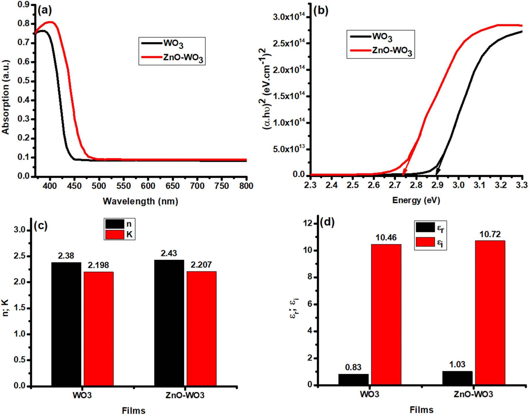 | ||
| Fig. 3 (a) UV-vis absorption, (b) Tau'c plots, (c) calculated values of refractive index and extinction coefficient, (d) calculated values of real and imaginary dielectric constant for WO3 and ZnO–WO3. | ||
The photoluminescence (PL) spectra of WO3 and ZnO–WO3 films were showed the excitation wavelength of 402 nm for ZnO–WO3 and 382 nm for WO3. The observed optical transitions are confirmed by the good alignment of these excitation wavelengths with the UV-vis absorption measurements.56 A redshift in the PL emission from the ZnO–WO3 film indicates that the ZnO inclusion has changed the band structure.57 This change results from Zn2+ doping-induced defect states that modify the kinetics of charge carrier recombination. Specifically in the higher-wavelength region, the ZnO–WO3 film exhibits a notable decrease in defect-related emission intensity, indicating enhanced crystallinity and fewer non-radiative recombination sites. Defect peak suppression points to improved charge carrier transit and decreased trap-assisted recombination, both of which are essential for a successful ETL in PSCs.57 By facilitating better electron extraction and transport, the redshift and decreased defect intensity minimize energy losses and raise the overall efficiency of perovskite solar cells.57,58 Average carrier lifetimes for WO3 and ZnO–WO3 ETLs were extracted by fitting the time-resolved photoluminescence (TRPL) data with a triple-exponential decay model (Fig. 4b). A remarkable average decay duration of around 119 ns was observed for WO3, suggesting considerable carrier trapping or defect-related recombination suppression that might restrict effective charge extraction.59 The ZnO–WO3 composite, on the other hand, had a lower average decay time of 13.5 ns, indicating decreased trap-assisted recombination and quicker carrier dynamics.59 The ZnO incorporation to WO3 improved the ETL's capacity for charge transfer and extraction, which made it more appropriate for high-performance PSC applications. Superior device efficiency may result from this enhanced dynamic behavior, which may make it easier to pump electrons into the ETL from the perovskite absorber layer.59
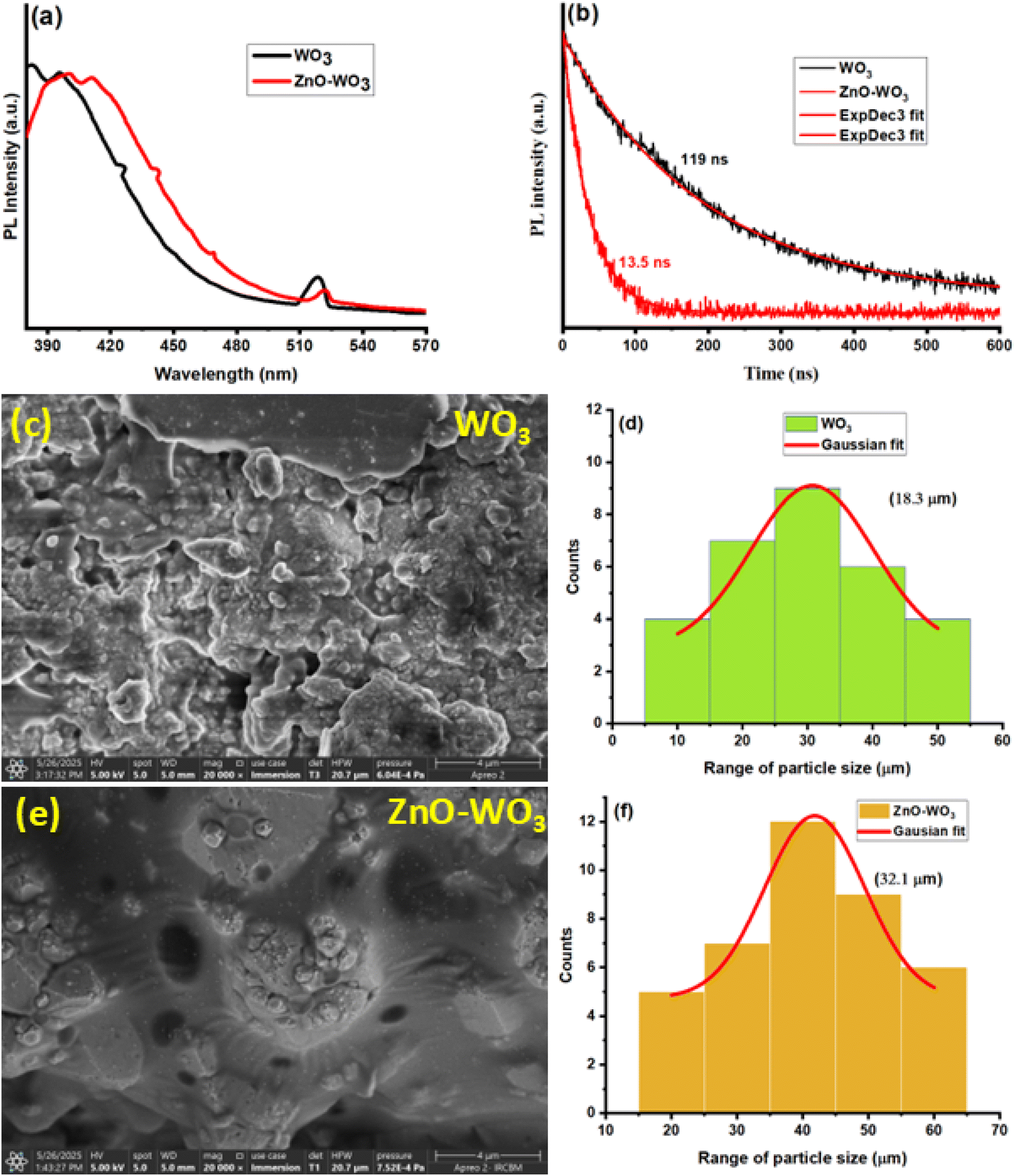 | ||
| Fig. 4 (a) PL, (b) time resolved PL, (c–f) SEM images with corresponding particle size distributions of WO3 and ZnO–WO3. | ||
The surface morphology and grain size distribution of WO3 and ZnO–WO3 films, as determined by SEM and particle size analysis, are shown in Fig. 4c–f. The WO3 film in Fig. 4c has smaller, agglomerated grains and a compact but irregular morphology, while Fig. 4d shows the matching particle size distribution with an average grain size of 18.3 μm.60 On the other hand, the ZnO–WO3 film in Fig. 4e exhibits bigger, clearly defined spherical aggregates together with a more consistent and smoother surface shape.61 Fig. 4f's size distribution shows a noticeably higher average particle size of 32.1 μm. For ETLs in PSCs, the addition of ZnO to WO3 improves film uniformity and encourages grain development.62 Smoother carrier paths and less charge trapping and recombination are made possible by larger grain sizes and better morphology, which also lowers grain boundary density. According to these structural enhancements, the ZnO–WO3 composite is a better ETL option than virgin WO3 for improving PSC performance.62,63
3.3. Photovoltaic performance
Three PSCs devices were constructed with the configurations (FTO\TiO2\CsPbIBr2\Spiro-OMeTAD\Au), (FTO\TiO2\WO3\CsPbIBr2\Spiro-OMeTAD\Au), and (FTO\TiO2\ZnO–WO3\CsPbIBr2\Spiro-OMeTAD\Au) as shown in Fig. 5a to assess the efficiency of the produced films as electron transport layers (ETLs). To modulate the conduction band offset (CBO) between TiO2 and CsPbIBr2 and enable effective charge transfer, ZnO–WO3 between TiO2 and the perovskite layer is essential.64 Electron–hole pairs are created when the perovskite absorber absorbs light. To promote a cascade-like electron transport process, electrons from the perovskite's conduction band (CB) are injected into ZnO–WO3 CB and then into TiO3. The perovskite layer's electron–hole recombination is greatly decreased by this structured energy alignment, improving the efficiency of charge collecting.64 The J–V curves and derived photovoltaic characteristics for three perovskite solar cells with various ETL setups are shown in Fig. 5b–c: Device-1 (FTO\TiO2\CsPbIBr2\Spiro-OMeTAD\Au), Device-2 (FTO\TiO2\WO3\CsPbIBr2\Spiro-OMeTAD\Au), and Device-3 (FTO\TiO2\ZnO–WO3\CsPbIBr2\Spiro-OMeTAD\Au). The following formulae are used to compute the efficiency (η) and fill factor (FF):65
 | (4) |
 | (5) |
 | ||
| Fig. 5 (a) TiO2\ZnO–WO3 ETLs-based device (b) J–V measurement (c) calculated values of open-circuit voltage and short-circuit current density (d) calculated values of fill factor and power conversion efficiency for TiO2, TiO2\WO3 and TiO2\ZnO–WO3 ETLs-based PSCs devices. | ||
Device-1 displays a power conversion efficiency (PCE) of 9.35%, a fill factor (FF) of 0.831, a JSC of 9.97 mA cm−2, and a VOC of 1.129 V. The addition of WO3 between the perovskite and TiO2 in Device-2 raises the PCE to 10.26%, the FF to 0.841, the JSC to 10.65 mA cm−2, and the VOC to 1.146 V. This enhancement results from WO3 advantageous conduction band edge alignment, which lowers energy losses and facilitates effective electron extraction from the perovskite layer to the ETL.66 With a VOC of 1.164 V, JSC of 12.95 mA cm−2, FF of 0.854, and PCE of 12.87%, Device-3 performs the best. As shown by longer carrier lifetimes in TR-PL measurements, the improvement in Device-3 results from the addition of ZnO to the WO3 layer, which inhibits trap-assisted recombination and enhances carrier transport. The TiO2\ZnO–WO3-based device performs noticeably better due to the combined effects of optimized energy level alignment by WO3, less recombination losses, and quicker carrier dynamics by ZnO.23,66
Electrochemical Impedance Spectroscopy (EIS) was conducted to analyze the charge transport and recombination processes within the fabricated perovskite solar cells (PSCs) employing WO3 and ZnO–WO3 as the electron transport layers (ETLs). The Nyquist plots for both devices are shown in Fig. 6a, where the charge transfer resistance (Rct) is represented by the semicircle diameter. It is clear that the ZnO–WO3-based device has a much smaller semicircle than the WO3-based device, which suggests a lower resistance to charge transfer.67 The retrieved parameters from EIS experiments are quantitatively shown in Fig. 6b, where the Rct values for TiO2/WO3 and TiO2/ZnO–WO3 ETL-based devices are 79 Ω and 21 Ω, respectively. The ZnO–WO3-based device's significant Rct decrease points to improved electron injection and transport at the ETL/perovskite interface.68 Furthermore, the WO3-based device's recombination resistance (Rrec), which measures the device's capacity to inhibit charge carrier recombination, is found to be 4342 Ω, whereas the ZnO–WO3-based device's Rrec rises to 4605 Ω.The ZnO–WO3-based device's higher Rrec value validates the suppression of charge recombination, which enhances photovoltaic performance overall.68
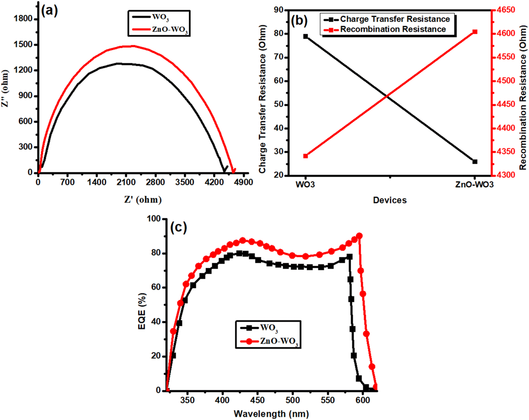 | ||
| Fig. 6 (a) EIS spectra (b) calculated values of charge transfer and recombination resistances (c) EQE for TiO2\WO3 and TiO2\ZnO–WO3 ETLs based devices. | ||
Fig. 6c shows the External Quantum Efficiency (EQE) spectra for both devices, which further confirms the ZnO–WO3-based ETL's better charge-collecting efficiency. In the wavelength range of 350 to 600 nm, the ZnO–WO3-based device's EQE response shows an overall improvement, with a peak efficiency of about 95%, as opposed to the WO3-based device's roughly 85%.64 In line with the lower Rct and higher Rrec seen in the EIS study, this improvement suggests a more effective extraction and transport of photogenerated charge carriers. By facilitating higher electron mobility, reducing energy barrier mismatches, and minimizing recombination losses, ZnO–WO3 improves the power conversion efficiency (PCE) of PSCs, as confirmed by the increased EQE.69
4. Conclusions
The incorporation of ZnO–WO3 as an ETL between TiO2 and the perovskite absorber effectively reduces recombination losses, leading to improved charge extraction and transport in PSCs. The sol–gel spin coating method was employed to synthesize both WO3 and ZnO–WO3 films. XRD analysis confirms the monoclinic phase of WO3. Raman spectroscopy revealed additional ZnO vibrational modes, indicating lattice reinforcement and enhanced structural integrity. Optical studies reveal a redshifted absorption edge and reduced bandgap, promoting efficient light absorption. SEM shows that ZnO–WO3 films have larger, more uniform grains and smoother morphology than WO3, indicating improved film quality. Time-resolved photoluminescence shows reduced average decay time for ZnO–WO3, indicating faster carrier dynamics. PSCs were fabricated with both ETLs, and devices with ZnO–WO3 demonstrated superior performance, achieving a PCE of 12.87%. EIS analysis confirms reduced charge transfer resistance and improved recombination resistance, while EQE measurements show enhanced charge collection. These results highlight ZnO–WO3 as a promising ETL for advancing high-efficiency PSCs in future photovoltaic applications.Data availability
Data supporting this study are available from the corresponding author upon reasonable request.Conflicts of interest
The authors have no conflict of interest.Acknowledgements
The authors are thankful to the Deanship of Graduate Studies and Scientific Research at University of Bisha for supporting this work through the Fast-Track Research Support Program. Moreover, the authors extend their appreciation to the Deanship of Scientific Research and Graduate Studies at King Khalid University for funding this work through large research project under grant number RGP2/474/45.References
- K. Matschoss, S. Laakso and J. Rinkinen, Disruptions and energy demand: How Finnish households responded to the energy crisis of 2022, Energy Res. Soc. Sci., 2025, 121, 103977 CrossRef.
- G. Paul and M. Prakash, The Rise of Energy Independence in Solving the Global Energy Crisis: Breaking the Chains, in Digital Innovations for Renewable Energy and Conservation, IGI Global, 2025, pp. 351–368 Search PubMed.
- E. Lucchi, Active solar design principles for natural and architectural heritage, in Solar Energy Technologies in Cultural Heritage, Elsevier, 2025, pp. 215–259 Search PubMed.
- J. Suo, et al., The dual use of SAM molecules for efficient and stable perovskite solar cells, Adv. Energy Mater., 2025, 15(2), 2400205 CrossRef CAS.
- D. Koo, et al., Mesoporous structured MoS2 as an electron transport layer for efficient and stable perovskite solar cells, Nat. Nanotechnol., 2025, 20(1), 75–82 CrossRef CAS PubMed.
- P. Priyadarshini, S. Senapati and R. Naik, Lead-free organic inorganic hybrid halide perovskites: an emerging candidate for bifunctional applications, Renewable Sustainable Energy Rev., 2023, 186, 113649 CrossRef CAS.
- K. Sahoo, et al., Highly stable and luminescent formamidinium-based perovskite nanocrystal probe for temperature and mercury sensors and in vitro imaging in live cells, J. Mater. Chem. C, 2024, 12(42), 17315–17327 RSC.
- S.-Y. Zhang, et al., Optimizing ETL/CsPbBr3 buried interface contact for enhanced efficiency and stability of inorganic perovskite solar cells, Rare Met., 2025, 1–11 Search PubMed.
- M. S. Uddin, et al., Achieving Over 28% Efficiency in Inorganic Halide Perovskite Ca3AsI3: Optimization of Electron Transport Layers via DFT, SCAPS-1D, and Machine Learning, J. Phys. Chem. Solids, 2025, 112622 CrossRef CAS.
- M. I. Khan, et al., Enhancing efficiency in double perovskite solar cells through bandgap reduction via organic polymer doping, Results Chem., 2025, 13, 101999 CrossRef.
- E. Danladi, E. E. Oguzie and F. I. Ezema, Challenges and outlooks on stability of inverted perovskite solar cells: a review insight, Multiscale Multidiscip. Model. Exp. Des., 2025, 8(1), 119 CrossRef.
- N. Pai and D. Angmo, Powering the Future: Opportunities and Obstacles in Lead-Halide Inorganic Perovskite Solar Cells, Advanced Science, 2025, 2412666 CrossRef CAS PubMed.
- R. Basu, et al., Comprehensive Numerical Simulation and Optimization of Lead-free Graded 2D-3D Perovskite Solar Cells, Sol. Energy, 2025, 287, 113204 CrossRef.
- A. Mujtaba, et al., Improved the Performance of Mixed Halide Perovskite Solar Cells through Crystal Engineering and by the Alignment of Energy Band Edges, New J. Chem., 2025, 49, 9233–9242 RSC.
- T. Du and L. Jin, Solvent engineering of SnO2 ETL for enhanced performance of carbon-based CsPbIBr2 PSCs, J. Sol-Gel Sci. Technol., 2025, 1–10 Search PubMed.
- J. Bi, et al., Modifying buried interface via 6-aminonicotinic acid molecule dipolar layer for efficient and stable inorganic perovskite solar cells, J. Power Sources, 2025, 628, 235943 CrossRef CAS.
- M. Islam, M. Shaikh and A. Kumar, Dual-and triple-absorber solar cell architecture achieves significant efficiency improvements, J. Comput. Electron., 2025, 24(1), 27 CrossRef CAS.
- M. S. Hasan, O. A. A. Ali, D. I. Saleh, M. Awais, M. Iqbal, M. Aslam and M. I. Irfan, Enhanced the efficiency and current density by structural modifications and conduction band shifting in lead-based mixed halide perovskite solar cells, Solid State Commun., 2025, 399, 115885 CrossRef CAS.
- R. Holfeuer, et al., Printed CsMg–ZnO ETLs achieve over 9% efficiency in PbS quantum dot solar cells, Mater. Today Energy, 2025, 48, 101813 CrossRef CAS.
- M. A. Mahmud, et al., Low temperature processed ZnO thin film as electron transport layer for efficient perovskite solar cells, Sol. Energy Mater. Sol. Cells, 2017, 159, 251–264 CrossRef CAS.
- J. Zhou, et al., Low-temperature aqueous solution processed ZnO as an electron transporting layer for efficient perovskite solar cells, Mater. Chem. Front., 2017, 1(5), 802–806 RSC.
- J.-X. Song, et al., Low-temperature-processed metal oxide electron transport layers for efficient planar perovskite solar cells, Rare Met., 2021, 40, 2730–2746 CrossRef CAS.
- Y. You, et al., TiO2/WO3 bilayer as electron transport layer for efficient planar perovskite solar cell with efficiency exceeding 20, Adv. Mater. Interfaces, 2020, 7(1), 1901406 CrossRef CAS.
- S. Moeini, M. Noori and A. Abbasiyan, Efficiency enhancement in 4T perovskite/Si tandem solar cell by charge extraction management, Sol. Energy Mater. Sol. Cells, 2025, 285, 113510 CrossRef CAS.
- H. Mahdhi, et al., Impact of Calcium Doping on the Properties of ZnO Thin Films: A Structural and Optical Analysis, J. Alloys Compd., 2025, 179291 CrossRef CAS.
- A. Mujtaba, et al., Impact of CsPbI3 incorporation on the structural, optical, and electrical properties of mixed-halide perovskite solar cells, J. Sol-Gel Sci. Technol., 2025, 1–11 Search PubMed.
- R. Biswas and S. Chatterjee, Effect of surface modification via sol-gel spin coating of ZnO nanoparticles on the performance of WO3 photoanode based dye sensitized solar cells, Optik, 2020, 212, 164142 CrossRef CAS.
- Y. Guo, et al., Highly efficient CsPbIBr 2 perovskite solar cells with efficiency over 9.8% fabricated using a preheating-assisted spin-coating method, J. Mater. Chem. A, 2019, 7(32), 19008–19016 RSC.
- J. Wang, W. Yu and S. Xu, Simultaneous regulation of grain size and interface of single-crystal ultrahigh-nickel LiNi0. 9Co0. 055Mn0. 045O2 via one-step Li2ZrO3 coating, J. Colloid Interface Sci., 2025, 685, 427–436 CrossRef CAS PubMed.
- X. Su, et al., In situ etching WO3 nanoplates: hydrothermal synthesis, photoluminescence and gas sensor properties, Mater. Res. Bull., 2010, 45(12), 1960–1963 CrossRef CAS.
- J. Han, et al., Enhanced NOx gas sensing properties of ordered mesoporous WO3/ZnO prepared by electroless plating, Adv. Mater. Interfaces, 2018, 5(9), 1701167 CrossRef.
- M. Khan, et al., Characterizations of multilayer ZnO thin films deposited by sol–gel spin coating technique, Results Phys., 2017, 7, 651–655 CrossRef.
- H. Abdullah, et al., Effect of Zn (O, S) Synthesis Temperature to Photocatalytic Hydrogen Evolution Performance, in Journal of Physics: Conference Series, IOP Publishing, 2019 Search PubMed.
- B. Subash and R. Sasikala, High-performance photocatalytic and antibacterial properties of WO3/ZnO honeycomb structures: synthesis and mechanistic insights, J. Iran. Chem. Soc., 2025, 1–21 Search PubMed.
- M.-S. Wong, et al., Influence of crystallinity and carbon content on visible light photocatalysis of carbon doped titania thin films, J. Mol. Catal. A: Chem., 2008, 279(1), 20–26 CrossRef CAS.
- S. Das, et al., A facile microwave-assisted nanoflower-to-nanosphere morphology tuning of CuSe1–xTe1+x for optoelectronic and dielectric applications, ACS Appl. Nano Mater., 2023, 6(7), 5298–5312 CrossRef CAS.
- P. Priyadarshini, et al., Zn doping induced optimization of optical and dielectric characteristics of CuInSe2 nanosheets for optoelectronic device applications, J. Alloys Compd., 2023, 945, 169222 CrossRef CAS.
- A. Mujtaba, et al., Enhanced the efficiency of TMs (Co and Ag) doped lead based mixed halides perovskite solar cells through the conduction band gap engineering, J. Indian Chem. Soc., 2025, 102(4), 101618 CrossRef CAS.
- A. Mujtaba, et al., Green hydrothermal synthesis of Mg-doped transition metal dichalcogenides using Camellia sinensis extract for enhanced energy storage, J. Sol-Gel Sci. Technol., 2025, 1–14 Search PubMed.
- A. Bokuniaeva and A. Vorokh, Estimation of particle size using the Debye equation and the Scherrer formula for polyphasic TiO2 powder, in Journal of Physics: Conference Series, IOP Publishing, 2019 Search PubMed.
- F. Motazedian, et al., Determining intrinsic stress and strain state of fibre-textured thin films by X-ray diffraction measurements using combined asymmetrical and Bragg-Brentano configurations, Mater. Des., 2019, 181, 108063 CrossRef CAS.
- R. F. Garcia-Sanchez, et al., Thermal effects associated with the Raman spectroscopy of WO3 gas-sensor materials, J. Phys. Chem. A, 2013, 117(50), 13825–13831 CrossRef CAS PubMed.
- M. Šćepanović, et al., Raman study of structural disorder in ZnO nanopowders, J. Raman Spectrosc., 2010, 41(9), 914–921 CrossRef.
- M. Alzaid, Recent progress in the role of two-dimensional materials as an efficient charge transport layer in perovskite solar cells, Int. J. Energy Res., 2021, 45(9), 12598–12613 CrossRef CAS.
- Q. Deng, et al., Remarkable optical red shift and extremely high optical absorption coefficient of V-Ga co-doped TiO2, J. Appl. Phys., 2012, 112(1), 013523 CrossRef.
- A. Karamat, et al., Revolutionizing photocatalysis: synergistic enhancement of structural, optical, and photodegradation properties in Be-doped V2O5 nanoparticles for efficient methylene blue removal, Results Chem., 2024, 8, 101600 CrossRef CAS.
- W.-J. Ho, et al., Improving photovoltaic performance of silicon solar cells using a combination of plasmonic and luminescent downshifting effects, Appl. Surf. Sci., 2018, 439, 868–875 CrossRef CAS.
- A. Dolgonos, T. O. Mason and K. R. Poeppelmeier, Direct optical band gap measurement in polycrystalline semiconductors: A critical look at the Tauc method, J. Solid State Chem., 2016, 240, 43–48 CrossRef CAS.
- A. Mujtaba, et al., Tailoring the structural, optical, photoluminescence, dielectric and electrical properties of Zn0·6Ni0·2Mg0·2Fe2–xLaxO4 (x = 0.00, 0.0125, 0.0250, 0.0375), J. Mater. Res. Technol., 2023, 23, 4538–4550 CrossRef CAS.
- E. Eren, et al., Enhanced electrochromic performance of WO3 hybrids using polymer plasma hybridization process, Synth. Met., 2018, 235, 115–124 CrossRef CAS.
- T. Xu, et al., Significantly enhanced photocatalytic performance of ZnO via graphene hybridization and the mechanism study, Appl. Catal., B, 2011, 101(3–4), 382–387 CrossRef CAS.
- H. Pan, et al., Advances in design engineering and merits of electron transporting layers in perovskite solar cells, Mater. Horiz., 2020, 7(9), 2276–2291 RSC.
- Ihtisham-ul-haq, et al., Enhancing efficiency of Cs2AgBiBr6 double perovskite solar cells through bandgap reduction by molybdenum doping, J. Korean Ceram. Soc., 2025, 62, 1–11 CrossRef.
- M. Sajjad, et al., Dual solutions of magnetohydrodynamics Al2O3+ Cu hybrid nanofluid over a vertical exponentially shrinking sheet by presences of joule heating and thermal slip condition, CFD Lett., 2022, 14(8), 100–115 CrossRef.
- A. Z. Muaawia, et al., Enhanced medicinal applications of Co-doped Zn0. 5Ni0. 5Fe2-xO4 for (X = 0.00 and 0.0250) soft ferrites: a structural analysis, J. Appl. Math., 2023, 1(2), 237 CrossRef.
- Y. Zou, et al., Structural and optical properties of WO3 films deposited by pulsed laser deposition, J. Alloys Compd., 2014, 583, 465–470 CrossRef CAS.
- P. Sharma, S. K. Tiwari and P. B. Barman, Abnormal red shift in photoluminescence emission of ZnO nanowires, J. Lumin., 2022, 251, 119231 CrossRef CAS.
- M. I. Khan, et al., Enhanced efficiency of CsPbIBr2 perovskite solar cells through dual-layer ETL engineering, J. Sol-Gel Sci. Technol., 2024, 111(3), 754–765 CrossRef CAS.
- X. Yu, et al., Fullerene modification of WO3 electron transport layer toward high-efficiency MA-free perovskite solar cells with eliminated light-soaking effect, Interdiscip. Mater., 2023, 2(3), 459–469 CAS.
- Z. Gu, et al., Controllable assembly of WO3 nanorods/nanowires into hierarchical nanostructures, J. Phys. Chem. B, 2006, 110(47), 23829–23836 CrossRef CAS PubMed.
- D. O. Alshahrani, et al., Tailoring the tungsten sulfide nanoparticles by nickel doping for high-performance energy storage application, J. Indian Chem. Soc., 2025, 102(6), 101709 CrossRef CAS.
- J. Huang, et al., Flower-like and hollow sphere-like WO3 porous nanostructures: Selective synthesis and their photocatalysis property, Mater. Res. Bull., 2012, 47(11), 3224–3232 CrossRef CAS.
- K. Mahmood, et al., Highly efficient perovskite solar cells based on a nanostructured WO3–TiO2 core–shell electron transporting material, J. Mater. Chem. A, 2015, 3(17), 9051–9057 RSC.
- B. S. Almutairi, et al., Impact of La doping on the optoelectronic and structural properties of CsPbIBr2 perovskite solar cell, Opt. Mater., 2024, 152, 115415 CrossRef CAS.
- M. Khan, et al., Effect of silver (Ag) ions irradiation on the structural, optical and photovoltaic properties of Mn doped TiO2 thin films based dye sensitized solar cells, Ceram. Int., 2021, 47(11), 15801–15806 CrossRef CAS.
- F. Zhao, et al., Effect of Li-doped TiO2 layer on the photoelectric performance of carbon-based CsPbIBr2 perovskite solar cell, J. Alloys Compd., 2023, 930, 167377 CrossRef CAS.
- M. Liberatore, et al., Using EIS for diagnosis of dye-sensitized solar cells performance, J. Appl. Electrochem., 2009, 39, 2291–2295 CrossRef CAS.
- Z. Zhang, et al., Toward high-performance electron/hole-transporting-layer-free, self-powered CsPbIBr2 photodetectors via interfacial engineering, ACS Appl. Mater. Interfaces, 2020, 12(5), 6607–6614 CrossRef CAS PubMed.
- D. Wang, et al., High-Efficiency Carbon-Based CsPbIBr2 Solar Cells with Interfacial Energy Loss Suppressed by a Thin Bulk-Heterojunction Layer, Sol. RRL, 2021, 5(9), 2100375 CrossRef CAS.
| This journal is © The Royal Society of Chemistry 2025 |