
 Open Access Article
 This Open Access Article is licensed under a Creative Commons Attribution-Non Commercial 3.0 Unported Licence
Investigation of C and Si-doped 2D germanene quantum dots for potential nanotechnology applications
Hoang Van Ngoc *ab and
Trieu Quynh Trangc
*ab and
Trieu Quynh Trangc
aAtomic Molecular and Optical Physics Research Group, Institute for Advanced Study in Technology, Ton Duc Thang University, Ho Chi Minh City, Vietnam. E-mail: hoangvanngoc@tdtu.edu.vn
bFaculty of Electrical and Electronics Engineering, Ton Duc Thang University, Ho Chi Minh City, Vietnam
cNam Dinh Teacher Training's College, Nam Dinh City, Nam Dinh Province, Vietnam
First published on 6th June 2025
Abstract
In this study, the structural, electronic, and optical properties of pristine and doped two-dimensional germanene quantum dots (GeQDs) were systematically investigated using first-principles calculations based on density functional theory (DFT). The model systems consist of monolayer GeQDs comprising 37 Ge atoms with hydrogen-passivated edges, including pristine, carbon-doped, and silicon-doped configurations. All structures are found to be dynamically stable, exhibit non-magnetic metallic behavior, and show distinctive structural modifications upon doping. Notably, carbon doping significantly reduces the buckling height of the quantum dots due to its smaller atomic radius and higher electronegativity. Multi-orbital hybridization analysis reveals substantial changes in electronic orbital interactions, particularly in the Si-doped structure. Charge density difference analysis indicates that carbon atoms act as charge acceptors, while silicon atoms donate charge to the surrounding Ge lattice. Optical property calculations show strong anisotropic absorption behavior, with all configurations demonstrating pronounced absorption in the ultraviolet region and moderate absorption in the visible range. These findings suggest that pristine and doped GeQDs hold promise for applications in nanoscale electronic and optoelectronic devices, including ultraviolet photodetectors, plasmonic components, and next-generation integrated circuits.
1. Introduction
In recent decades, the advancement of science and technology has become increasingly intertwined with the progress of nanotechnology, a field that has enabled significant breakthroughs in device miniaturization and performance enhancement. Nanomaterials often exhibit distinct physical and chemical properties compared to their bulk counterparts, primarily due to quantum confinement effects and the substantial increase in surface-to-volume ratio. When a material's dimensions are restricted in one, two, or all three spatial directions, the motion of electrons becomes confined, resulting in the quantization of energy levels. This confinement leads to discrete electronic states and pronounced quantum effects that are significantly more evident than in bulk, three-dimensional systems.Among the emerging materials at the nanoscale, two-dimensional (2D) systems have garnered considerable attention due to their remarkable potential in electronic, optoelectronic, sensing, and energy-related applications. Materials such as silicene,1–4 germanene,5–8 borophene,9–12 and phosphorene13–16 have emerged as promising candidates, each possessing unique structural and electronic characteristics. These 2D materials often adopt a honeycomb lattice configuration analogous to that of graphene-the first isolated two-dimensional material-exhibiting exceptional properties such as high mechanical strength, excellent electrical conductivity, and efficient thermal transport.
Nevertheless, despite its exceptional attributes, graphene suffers from critical limitations, notably its zero band gap and the high cost associated with its synthesis.17–20 These drawbacks have spurred extensive research into alternative 2D materials that offer tunable band gaps and more practical pathways for large-scale production and integration into next-generation nanoelectronic systems.
The continuous pursuit of novel materials remains a cornerstone in advancing industrial revolutions, particularly within the high-technology sector. These materials not only enhance the performance of existing systems but also pave the way for the emergence of entirely new technologies. In the semiconductor industry, the growing demand for increasingly compact and high-speed devices has driven the rapid evolution of microchip fabrication, with state-of-the-art integrated circuits now operating at feature sizes of only a few nanometers.
Within this technological landscape, germanene-a monolayer of germanium atoms arranged in a honeycomb lattice – has emerged as a subject of significant scientific interest. While pristine germanene is a semimetal with a nearly zero band gap, its electronic structure can be effectively modulated through various approaches such as atomic doping,21–23 surface functionalization,8,24,25 and the application of external electric or strain fields.26–28 These modifications have demonstrated the potential to open a finite band gap, thereby expanding germanene's applicability in semiconductor and optoelectronic devices.
Structurally, germanene features a Ge–Ge bond length of approximately 2.48 Å, and its electronic configuration is governed by partially hybridized orbitals that form weak π bonds. This incomplete hybridization induces a characteristic buckling of the atomic plane, with a buckling height of roughly 0.69 Å.29 Such buckling not only distinguishes germanene from its planar analogue, graphene, but also plays a crucial role in determining its electronic and optical behavior. Adjusting the buckling and bonding configuration-via doping, strain engineering, or surface modification-can significantly tailor germanene's material properties, making it a flexible platform for integration into diverse nanoelectronic and photonic technologies.30–32
Experimental efforts have demonstrated the in situ growth of germanene monolayers on Au(111) substrates using molecular beam epitaxy, revealing ordered domains with nearly flat honeycomb patterns.33 First-principles calculations further verify that germanene is dynamically stable and hosts linear band crossings at the Fermi level, where charge carriers behave as massless Dirac fermions.34 In contrast to graphene, the buckled structure of germanene results in a larger spin–orbit gap (∼24 meV), making it a promising candidate for quantum spin Hall devices and enabling bandgap tunability through external electric fields or surface functionalization.7 These distinct structural and electronic characteristics position germanene as a highly versatile material for applications in next-generation nanoelectronics and spintronics.
Beyond monolayer germanene, considerable research attention has also been directed toward lower-dimensional derivatives such as germanene nanoribbons,35–38 germanene nanotubes,39,40 and germanene quantum dots (GeQDs).41–43 Germanene nanoribbons, as quasi-one-dimensional (1D) systems, allow electron delocalization primarily along a single axis, whereas GeQDs represent zero-dimensional (0D) structures in which electronic motion is confined in all three spatial dimensions. This complete quantum confinement leads to pronounced discretization of energy levels and induces novel quantum phenomena that are absent in 1D and 2D systems.
Previous investigations of GeQDs with varying shapes and sizes have revealed a strong dependence of their electronic and optical characteristics on geometrical and structural parameters. For instance, edge functionalization using elements such as hydrogen (H), fluorine (F), or chlorine (Cl) has been shown to modulate the band gap within the range of 0.72 eV to 0.89 eV, concurrently altering the electronic band structure and the density of states.43 Moreover, the size of the quantum dot plays a crucial role: as the number of constituent atoms increases, the density of localized electronic states also rises, thereby affecting the system's overall electronic response.41 Importantly, a simultaneous increase in quantum dot size and the application of an external electric field can induce a redshift in the optical absorption spectrum, offering a viable route for tuning the optical response to meet specific application requirements. In the context of renewable energy, GeQDs have also shown promise in solar energy conversion technologies, particularly due to their strong light absorption in the visible spectral region.44 These findings underscore the significance of structural morphology-specifically shape, size, and edge passivation-in governing the fundamental electronic and optical behavior of GeQDs, and highlight their potential in a wide range of nanoscale device applications.
Hydrogen-passivated two-dimensional germanene quantum dots (2D GeQDs) represent a promising research direction due to their quantum confinement effects and tunable properties, particularly in the context of nanoscale device engineering. This study aims to provide a comprehensive investigation of this material system, exploring both its electromagnetic and optical characteristics as a foundation for future studies and as a reference point for potential applications in next-generation electronic and optoelectronic technologies. The introduction of dopants not only enhances the tunability of GeQDs' intrinsic properties but also broadens their applicability across various domains of advanced nanotechnology, including nanoscale transistors, photodetectors, and energy-harvesting devices.
Carbon and silicon were selected as dopants for GeQDs due to their group IV chemical similarity to germanium, which allows for substitutional doping with minimal lattice disruption. This facilitates the formation of stable doped structures without introducing significant structural defects or strain. Despite belonging to the same group, carbon and silicon exhibit contrasting atomic sizes and electronegativities, which enables the systematic investigation of how these parameters affect the structural, electronic, and optical properties of GeQDs. Carbon, being smaller and more electronegative than Ge, induces strong charge localization and planarization effects, leading to significant changes in the buckling height and local electronic environment. Silicon, with a similar size to Ge but lower electronegativity, acts as a charge donor and modifies the orbital hybridization in a distinct way, particularly influencing the high-energy electronic states and optical response. This complementary behavior provides a controlled comparative framework to understand how dopants with different physical and chemical properties impact quantum dot behavior.
Other dopants, such as group III elements (e.g., B, Al) or group V elements (e.g., N, P, As), could offer alternative or improved functionalities: group III dopants may introduce p-type characteristics, useful for designing heterojunctions or diode-like behaviors. Group V dopants may act as n-type donors and alter the electronic density of states in a way that enhances charge transport or photoresponse. Transition metals (e.g., Ti, Mn) could introduce magnetic or spintronic functionalities, opening paths for quantum spintronic applications. Future work could explore such dopants to further tailor the optoelectronic properties of GeQDs for specialized device applications.
2. Methods
In this work, the structural, electronic, and optical properties of pristine and doped two-dimensional germanene quantum dots (GeQDs) were investigated using first-principles calculations based on density functional theory (DFT), as implemented in the Vienna Ab initio Simulation Package (VASP). The quantum dot model comprises 37 germanium (Ge) atoms arranged in a monolayer honeycomb-like lattice, with hydrogen (H) atoms passivating the edge Ge atoms to simulate chemically stable boundaries. Doping was introduced by substituting selected central Ge atoms with carbon (C) or silicon (Si) atoms to examine the influence of atomic substitution on the physical properties of the system.The calculations employed the Generalized Gradient Approximation (GGA) with the Perdew–Burke–Ernzerhof (PBE) exchange–correlation functional. The interaction between core and valence electrons was treated using the Projector Augmented-Wave (PAW) method. Geometry optimizations were performed until the residual forces on all atoms were less than 0.01 eV Å−1 and the total energy convergence criterion was set to 10−7 eV. To ensure the reliability and accuracy of the DFT calculations, systematic convergence tests were conducted for both the plane-wave energy cutoff and k-point sampling. A plane-wave energy cutoff of 500 eV was adopted, which provided total energy convergence within 1 meV per atom. For Brillouin zone integration, a Monkhorst–Pack grid of 5 × 5 × 1 was employed and tested to ensure the accuracy of total energy and electronic structure calculations. This k-point mesh was found to be sufficient for the finite-sized two-dimensional quantum dot systems studied here, where a large vacuum spacing (20 Å) was also applied to eliminate spurious interactions between periodic images.
Limitations of the DFT method and the GGA-PBE functional: while the generalized gradient approximation with the Perdew–Burke–Ernzerhof (GGA-PBE) functional provides a good balance between computational efficiency and accuracy for structural and electronic property calculations, it has known limitations. In particular, GGA-PBE tends to underestimate band gaps in semiconductors and insulators due to its approximate treatment of exchange-correlation interactions. This may lead to inaccuracies in the predicted optical transition energies, especially in the visible and ultraviolet regions. Additionally, van der Waals (vdW) interactions are not adequately captured by standard GGA-PBE, although in this study, such long-range interactions are less critical due to the quantum dot system being finite and passivated. Finally, many-body effects, excitonic interactions, and temperature effects are not included in the DFT-GGA framework, which can further impact the accuracy of optical property predictions. Despite these limitations, GGA-PBE remains a reliable tool for qualitative and comparative analyses, particularly when the focus is on trends and relative changes induced by doping.
3. Electromagnetic properties
Fig. 1 presents the atomic structures of the pristine and doped configurations of the 2D germanene quantum dots (GeQDs), with single-atom substitution by carbon (C) and silicon (Si). A clear buckled geometry characteristic of the germanene framework is evident in all three configurations. As summarized in Table 1, the buckling height of the pristine 2D GeQDs is calculated to be 0.647 Å, which is in good agreement with previously reported values for monolayer germanene, such as 0.635 Å (ref. 45) and 0.676 Å.46 This indicates that the transition from an extended germanene sheet to a quantum-confined 2D GeQD structure does not significantly alter the vertical displacement within the atomic plane, preserving the intrinsic buckled configuration. | ||
| Fig. 1 (a) Side view and (b) top view of pristine configuration; (c) C-doped 2D GeQDs; (d) Si-doped 2D GeQDs. | ||
| Configurations | d1 (Å) | d2 (Å) | α (°) | Ef (eV) | Δ (Å) | μ (μB) |
|---|---|---|---|---|---|---|
| Pristine | 2.439 | x | 112.34 | x | 0.647 | 0 |
| C-doped GeQDs | 2.445 | 1.958 | 114.77 | −1.35 | 0.232 ÷ 0.462 | 0 |
| Si-doped GeQDs | 2.436 | 2.373 | 112.92 | −0.98 | 0.610 ÷ 0.619 | 0 |
In terms of bond length, the average Ge–Ge distance in pristine GeQDs was found to be 2.439 Å, which is slightly shorter than the 2.56 Å observed in germanene structures7 and close to the value of 2.443 Å reported in ref. 47. Upon substitutional doping with either C or Si atoms, the Ge–Ge bond lengths remain largely unaffected, suggesting that the overall lattice retains good structural integrity. However, the introduction of dopant atoms leads to notable differences in local bonding. Specifically, the Ge–C bond length is calculated to be 1.958 Å, considerably shorter than the Ge–Si bond length of 2.373 Å. This shortening of the Ge–C bond implies a stronger local bonding interaction, consistent with higher bond strength.
This observation is further supported by the calculated formation energy of system:48
| Ef = Et − Epris + nEGe − nESi/C | (1) |
When calculating the formation energy per atom for the C- and Si-doped systems, we employed the following expression:
 | (2) |
The calculated formation energies per atom (Ef/a) for the C-doped and Ge-doped GeQD structures are −2.89 eV per atom and −2.65 eV per atom, respectively, both of which are less negative than that of monolayer germanene (−3.31 eV per atom49). This reduction in formation energy indicates that the doped GeQDs are thermodynamically less stable than the extended two-dimensional germanene sheet. The difference in stability can be primarily attributed to pronounced edge effects and the increased surface-to-volume ratio characteristic of the quantum dot morphology. Furthermore, the lack of long-range crystalline periodicity in the QDs gives rise to local structural distortions and undercoordinated atoms, which elevate the total energy and thus reduce the thermodynamic stability. Nevertheless, the negative values of formation energy confirm that both doped GeQDs remain thermodynamically stable.
The bond angle (α) formed between two adjacent Ge–Ge bonds remains nearly unchanged across all three configurations—pristine, C-doped, and Si-doped—and consistently falls below 120°, which is the ideal angle for a planar hexagonal lattice such as that of graphene. This deviation from ideal planarity reflects the intrinsic buckling present in the germanene framework and highlights the difference in orbital hybridization from the ideal sp2 configuration, suggesting partial sp3 character in the bonding environment of Ge atoms.
A notable structural response to doping is observed in the variation of buckling height. In the C-doped system, the buckling height is significantly reduced, ranging between 0.232 Å and 0.462 Å, in contrast to the 0.647 Å observed in the pristine structure. This flattening effect is likely attributed to the smaller covalent radius and higher electronegativity of the carbon atom, which promotes stronger in-plane bonding and reduces out-of-plane distortion. In comparison, the Si-doped structure exhibits only a slight reduction in buckling height, suggesting a comparatively weaker perturbation to the lattice geometry due to the similar atomic size and bonding characteristics of Si relative to Ge.
An additional and important observation is that all configurations—pristine, C-doped, and Si-doped—exhibit zero net magnetic moment. This indicates an absence of spontaneous magnetization and implies that the systems remain non-magnetic regardless of dopant type. This conclusion is corroborated by the spin-resolved density of states (DOS) shown in Fig. 2, where the spin-up and spin-down components are fully symmetric about the Fermi level. The preservation of spin symmetry confirms that neither C nor Si doping induces spin polarization in the GeQD system. Fig. 2 displays the calculated electronic band structures and total density of states (DOS) for the pristine, C-doped, and Si-doped 2D GeQD systems. All three configurations exhibit metallic characteristics. However, despite the absence of a band gap, the density of states at the Fermi level remains relatively low for all cases, indicating that these systems, while metallic, may exhibit limited electrical conductivity due to the modest availability of electronic states for conduction.
 | ||
| Fig. 2 Band structure and density of states of configuration: (a) pristine, (b) C-doped GeQDs, (c) Si-doped GeQDs. | ||
A comparative analysis reveals substantial differences between the pristine and doped systems, while the C- and Si-doped configurations exhibit notably similar band structures. This similarity suggests that both dopants exert a comparable influence on the local electronic environment within the GeQD lattice. In the energy range of −3 eV to 3 eV, which is critical for electronic transport and optical transitions, the peak DOS of the pristine system reaches approximately 40 states per eV. By contrast, the corresponding peak in both doped systems is reduced to about 30 states per eV, indicating a suppression of available electronic states in the vicinity of the Fermi level as a result of doping. This reduction could potentially influence carrier mobility and dynamic response under external perturbations such as applied electric fields or photoexcitation.
Furthermore, a shift in the dominant DOS peaks is observed: in the pristine configuration, the highest DOS peak is located in the conduction band, whereas in the doped structures, the most prominent peaks are concentrated within the valence band region. This redistribution of state density suggests that doping not only modifies the electronic density near the Fermi level but also alters the character and occupation of dominant electronic states, possibly due to changes in orbital hybridization or charge transfer mechanisms introduced by the dopant atoms.
The partial density of states (PDOS) for the Ge and dopant atoms in the pristine, C-doped, and Si-doped 2D GeQD configurations are shown in Fig. 3. In all three configurations, the Ge(4s) states are predominantly located in the lower energy region below −4 eV, suggesting that they are associated with stronger bonding levels and have minimal influence on the electronic structure near the Fermi level. Conversely, the Ge(px, py, pz) (p orbitals) states are concentrated around the Fermi level, highlighting their pivotal role in the formation of π and σ bonds within the crystal lattice. This distribution underscores the importance of p orbital hybridization in determining the electronic properties of the system.
 | ||
| Fig. 3 PDOS of (a) pristine GeQDs, (b) C-doped GeQDs, (c) Si-doped GeQDs. | ||
In the doped configurations, the introduction of C or Si atoms leads to the emergence of new localized states near the Fermi level, indicative of the interaction between the dopant atoms and the surrounding Ge lattice. This interaction results in multi-orbital hybridization, where the Ge orbitals overlap with those of the dopant atoms, forming stable Ge–C or Ge–Si bonds. The pronounced hybridization between the Ge and dopant orbitals is evident in the PDOS plots, reinforcing the findings from bond length and formation energy calculations, which highlighted the stable nature of the bonds formed upon doping.
In Fig. 3a, the partial density of states (PDOS) for the pristine configuration reveals that the largest peak is located at the Ge(4s) state, with a value of approximately 18 states per eV. In comparison, the corresponding peak in the C-doped configuration (Fig. 3b) is notably reduced to 10 states per eV, indicating a significant decrease in the contribution of the Ge(4s) orbital to the deep energy bands upon doping with carbon atoms. On the other hand, in the Si-doped configuration (Fig. 3c), the Ge(4s) peak increases slightly to 19 states per eV, closely resembling the value observed in the pristine system. The evident difference between the pristine and C-doped configurations suggests that carbon doping induces more pronounced charge redistribution and restructuring of the energy bands, thereby having a deeper impact on the electronic structure compared to silicon doping.
Focusing on the Ge(4pz) states, the pristine system shows a peak of 12 states/eV, whereas in the C-doped configuration, this peak sharply drops to 5.8 states per eV, further confirming that carbon doping significantly weakens the contribution of the p-orbitals oriented perpendicular to the plane. In contrast, the Si-doped configuration exhibits Ge(4pz) peaks and other p-state components that closely mirror those of the pristine system, reflecting the better orbital compatibility between silicon and germanium.
Another significant difference is observed in the positive energy region, where the unoccupied states in the conduction band reside. While both the pristine and C-doped configurations display a density of states extending from 0 to 5 eV, the Si-doped configuration shows conduction band states confined to the range from 0 to 3 eV. This narrowing of the conduction band suggests that silicon doping could influence the system's optical excitation properties at higher energies, potentially affecting its absorption spectrum and impacting future applications in optoelectronic devices.
In terms of multi-orbital hybridization, the pristine structure exhibits Ge(4s)–Ge(4px) hybridization in the energy ranges of −6 to −5.5 eV and −5 to −4.5 eV, which corresponds to the combination of s and p orbitals of Ge atoms, forming σ bonds within the crystal lattice. Additionally, in the energy region of 3 to 5 eV, hybridization between Ge(4s) and both Ge(4px) and Ge(4pz) orbitals is observed, indicative of weakly bound states and unoccupied states that are available for optical excitation. For the C-doped configuration, the hybridization becomes more intricate. In the energy range of −5 to −4 eV, three-dimensional hybridization involving Ge(4s), Ge(4px), and C(2py) orbitals is evident. The introduction of the C atom—being more electronegative and smaller than Ge—modifies the orbital orientations and generates new hybridization states, which may significantly influence the bond strength and electronic properties of the system.
In the Si-doped configuration, hybridization between Ge(4s), Ge(4px), and Si(3py) orbitals is also observed in the energy range from −5 to −4 eV. However, it is noteworthy that in the 3 to 5 eV region, there is a complete absence of significant electronic states, which sharply contrasts with the pristine and C-doped configurations. This lack of states may stem from a reduction in the density of unoccupied states, likely due to the weaker interaction between Ge and Si compared to the Ge–C bond, potentially leading to diminished optical absorption in this energy range.
Fig. 4 illustrates the charge density difference in 2D GeQDs upon doping with C (Fig. 4a) and Si (Fig. 4b) atoms. In Fig. 4a, the positively charged region (yellow) is clearly concentrated around the doped C atom, indicating that the C atom accumulates additional charge from the surrounding environment, particularly from neighboring Ge atoms. In contrast, Fig. 4b shows a negatively charged region (blue) surrounding the Si atom, signifying that Si loses charge and thus behaves as a charge donor within the system. This disparity can be attributed to the differing electronegativities of the atoms: the carbon atom (C) possesses a higher electronegativity than germanium (C = 2.55 > Ge = 2.01), which facilitates its tendency to attract electrons. Conversely, silicon (Si) has an electronegativity similar to or lower than that of Ge (Si = 1.90 < Ge = 2.01), which results in its tendency to donate charge. The charge redistribution phenomenon is not limited to the local doping site but also extends to neighboring Ge atoms, highlighting the influence of doping on the overall electronic structure of the system. Such changes in charge distribution may lead to significant modifications in the electrical, optical, and chemical properties of 2D GeQDs.
 | ||
| Fig. 4 Charge density difference in 2D GeQDs doped with C (a) and Si (b) (blue and yellow regions correspond to charge depleted and charge enhanced regions, respectively). | ||
4. Optical properties
Fig. 5 presents the dielectric function of pristine GeQDs as well as GeQDs doped with C and Si atoms. A notable observation is that the x and y components of both the real (Re) and imaginary (Im) parts of the dielectric function are in complete agreement across all configurations. This behavior reflects the symmetric and uniform atomic distribution within the xy plane, which is characteristic of a two-dimensional quantum dot structure. The coinciding components also serve as evidence for in-plane optical isotropy, suggesting that optical anisotropy predominantly occurs in the direction perpendicular to the plane, i.e., along the z-axis. For all configurations, the largest absorption peaks in the imaginary part of the dielectric function in the x/y direction appear in the low-energy region, below 1 eV, corresponding to the microwave spectral range. As the energy increases into the visible and ultraviolet regions, the absorption begins to decrease, indicating a reduction in optical absorption at higher energies. This trend suggests that GeQDs could be potential candidates for applications in microwave absorption or low-frequency sensing technologies. | ||
| Fig. 5 Dielectric function components of the pristine GeQDs configuration (a), C-doped GeQDs configuration (b), Si-doped GeQDs configuration (c). | ||
The plot of the real part of the dielectric function in the z-direction (Re(z)) exhibits distinctly different behavior from that observed in the x/y directions. In the energy range from 0 to 7 eV, the real part of the dielectric function remains nearly constant and parallel to the energy axis, indicating a weak dielectric response in the direction perpendicular to the plane. A clear peak emerges only around 8 eV, after which the plot declines rapidly, approaching a stable value at energies exceeding 9 eV. In this high-energy region, the dielectric function components in the x, y, and z directions converge, suggesting a significant reduction in optical anisotropy. This behavior implies that, at elevated energies, electromagnetic waves propagate through the material with similar interaction strengths in all directions.
Another important observation arises in the Si-doped configuration, where a minimum in the real part of the dielectric function in the x/y direction appears at approximately 5.2 eV, within the ultraviolet region. At this energy, Re(x/y) takes on a small negative value, signifying that the system can support electromagnetic wave propagation with minimal energy loss, characteristic of materials exhibiting plasmonic or low-loss optical transmission in the ultraviolet range. This phenomenon may open promising avenues for applications in optical transmission, plasmonic optical sensors, or small-scale nano-waveguide devices.
Fig. 6 presents the optical absorption coefficients of pristine GeQDs and those doped with C and Si atoms. As observed, the absorption coefficients in the x and y directions are identical across all configurations, reaffirming the in-plane optical isotropy of the two-dimensional GeQDs. This isotropy reflects the high structural symmetry and uniform electron distribution within the x0y plane, which is characteristic of two-dimensional materials with hexagonal or graphene-like geometries.
 | ||
| Fig. 6 Absorption coefficient components of pristine GeQDs configuration (a), C-doped GeQDs configuration (b), Si-doped GeQDs configuration (c). | ||
In the pristine and C-doped systems, the strongest absorption peak occurs along the z direction, corresponding to a wavelength of approximately 150 nm—within the near-ultraviolet (UV-C) spectral region. This suggests that these configurations exhibit pronounced ultraviolet absorption when the incident radiation is perpendicular to the atomic plane, indicating their potential utility in UV-sensitive devices such as photodetectors or protective coatings.
By contrast, in the Si-doped configuration, the most prominent absorption peak shifts to the in-plane x/y direction and occurs at a wavelength near 250 nm, also within the ultraviolet range. The variation in both the directionality and position of the peak absorption between the C- and Si-doped systems highlights the critical role of dopant species in modulating the spatial distribution of electronic states and optical transitions. These effects can be attributed to differences in electronegativity and atomic radius between the dopants (C and Si) and the host Ge atoms, which alter the local electronic structure and the density of states at excitation-relevant energy levels.
Notably, in the visible spectral range (approximately 450 nm and 600 nm) and the near-infrared region (around 1000 nm), the absorption coefficients in the x/y directions still exhibit distinct peaks—particularly in the Si-doped configuration. In contrast, the z components of the absorption coefficients in all configurations drop sharply to nearly zero for photon wavelengths exceeding 400 nm, indicating that the structures exhibit negligible absorption in the visible and infrared regions when the light is incident perpendicular to the material plane.
These findings demonstrate that the optical absorption characteristics of GeQDs are not only governed by their geometric and compositional structure but are also highly sensitive to the polarization direction of incident electromagnetic radiation. Specifically, the pristine and C-doped structures show strong ultraviolet absorption when the electric field is aligned along the z-axis, while the Si-doped structure exhibits enhanced absorption in the x0y-plane across a broader spectral range, including visible and near-infrared wavelengths. This polarization-dependent optical response underscores the tunable nature of GeQDs and highlights their potential for use in polarization-selective photodetectors, photovoltaic devices, and directional optical communication systems.
Fig. 7 shows the Joint Density of States (JDOS) for pristine, C-doped, and Si-doped GeQDs. The JDOS provides insight into the number of available electron–hole pairs that can be excited by incident photons of specific energies, thereby determining the likelihood of interband optical transitions. In the low-energy regime, for photon energies below 25 eV, the JDOS profiles for all three configurations are nearly identical, suggesting that in this energy range, the fundamental optical transition mechanisms remain largely unaffected by doping. This result indicates that while dopants significantly alter local electronic distributions and optical anisotropy, they exert minimal influence on the overall density of optically active states at lower excitation energies.
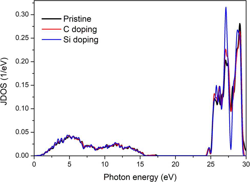 | ||
| Fig. 7 Joint density of states (JDOS) of pristine GeQDs and C, Si doped configurations. | ||
However, within the photon energy range below 1.3 eV, the JDOS remains nearly zero across all configurations, indicating the absence of available electron–hole transitions at these low energies. This implies that photons in the far-infrared and microwave spectral regions do not possess sufficient energy to induce optical transitions in the GeQDs systems under investigation. Consequently, these structures exhibit negligible optical activity in the low-energy regime, thereby limiting their potential use in infrared absorption or emission technologies.
As the photon energy increases beyond 25 eV, the JDOS profiles exhibit pronounced peaks, indicating a sharp rise in the number of electronic states capable of participating in optical transitions. In this high-energy regime, differences between the pristine and doped configurations become more distinct. Notably, the Si-doped structure displays the highest JDOS peak, suggesting that Si incorporation leads to a significant enhancement in the density of optically active states in the deep ultraviolet (DUV) region. This increase supports the conclusion that Si doping improves the material's optical transition efficiency at high photon energies, making it a promising candidate for applications in DUV optoelectronic devices.
Overall, the JDOS analysis confirms that the ultraviolet range is the most favorable for strong optical transitions in GeQDs-based systems, corresponding to the highest electron–hole generation density. While the visible region also supports optical transitions, the associated JDOS values are significantly lower, implying a reduced transition probability. Nonetheless, this moderate activity in the visible spectrum may still be advantageous for applications in photodetectors, light-emitting devices, and solar energy harvesting that operate within the visible light range.
The tunable electronic and optical properties of doped GeQDs suggest several promising applications in next-generation nanoscale devices. Specifically, the strong and anisotropic absorption in the ultraviolet (UV) region, especially prominent in the z-direction for pristine and C-doped systems, and in the in-plane directions for Si-doped systems, highlights their suitability for UV photodetector technologies.
Carbon doping leads to reduced buckling height and enhanced planarity, which improves carrier mobility and optical transition probability, crucial for efficient photodetection. Furthermore, the non-magnetic metallic behavior combined with dopant-induced charge redistribution creates built-in electric fields at the dopant sites, which can facilitate fast charge separation, improving photoresponsivity. The C-doped GeQDs, acting as strong electron acceptors, may function as efficient photoactive layers in UV photodetectors, where their high UV absorption enables strong photocurrent generation under low-intensity UV light. The Si-doped GeQDs, with enhanced charge donation and distinctive orbital hybridization, could serve in plasmonic nanodevices or UV filters, where fine-tuning the optical response is essential.
Beyond photodetection, the tunable band structure and strong direction-dependent absorption suggest potential use in: nanoscale field-effect transistors (FETs), where dopant-controlled conduction properties can be exploited for switching behavior. Quantum optoelectronic devices, where the zero-dimensional confinement and discrete energy levels of QDs benefit from the dopant-induced modulation of energy states. Thus, the ability to engineer optical anisotropy and electronic behavior through selective doping provides a versatile platform for customizing GeQDs for specific optoelectronic applications.
5. Conclusions
This study has systematically investigated the structural, electronic, and optical properties of two-dimensional germanene quantum dots (GeQDs) in their pristine form as well as when doped with carbon (C) and silicon (Si) atoms. All considered configurations exhibit non-magnetic metallic behavior, with the doping process inducing notable structural and electronic modifications. In particular, the introduction of C atoms significantly reduces the buckling height, indicating a stronger planarization effect compared to Si doping. Partial density of states (PDOS) and multi-orbital hybridization analyses revealed that while all systems share fundamental characteristics, the Si-doped configuration exhibits distinct orbital interactions, particularly in the high-energy regime. Charge density difference analysis further confirms the contrasting electronic roles of the dopant atoms: C atoms tend to attract electronic charge from surrounding Ge atoms, consistent with their higher electronegativity, whereas Si atoms act as charge donors. The optical response analysis shows that all systems exhibit low absorption in the far-infrared and microwave regions, with optical absorption increasing at higher photon energies. Anisotropic optical behavior is evident at photon energies below 9 eV, where isotropy is confined to the in-plane (x0y) directions. Above 9 eV, isotropy emerges in all spatial directions, indicating uniform electromagnetic interaction at high energies. Strong ultraviolet absorption was observed across all configurations, particularly in the z-direction for pristine and C-doped systems and in the x0y plane for the Si-doped configuration. Furthermore, although absorption in the visible region is relatively moderate, it remains sufficient to support optoelectronic applications. These findings highlight the potential of pristine and doped GeQDs for integration into nanoscale electronic and optoelectronic devices, such as high-performance transistors, ultraviolet photodetectors, and components for next-generation integrated circuits. The tunable electronic and optical properties via dopant selection provide a promising route for material engineering in quantum-scale systems.Data availability
Data supporting the findings of this study are available within the article.Author contributions
Hoang Van Ngoc surveyed, researched, studied, and set up the input files. Trieu Quynh Trang prepared the tables and drew the figures. Hoang Van Ngoc and Trieu Quynh Trang wrote the main manuscript. All authors reviewed the manuscript.Conflicts of interest
The authors declare that they have no conflicts of interest.Acknowledgements
The authors gratefully acknowledge the support of the High-Performance Computing system at the Institute for Advanced Study in Technology (IAST), Ton Duc Thang University.References
- A. Kara, et al., A review on silicene—new candidate for electronics, Surf. Sci. Rep., 2012, 67(1), 1–18 CrossRef CAS.
- G. Le Lay, Silicene transistors, Nat. Nanotechnol., 2015, 10(3), 202–203 CrossRef PubMed.
- A. Molle, et al., Silicene, silicene derivatives, and their device applications, Chem. Soc. Rev., 2018, 47(16), 6370–6387 RSC.
- D. Jose and A. Datta, Structures and chemical properties of silicene: unlike graphene, Acc. Chem. Res., 2014, 47(2), 593–602 CrossRef CAS PubMed.
- M. Derivaz, et al., Continuous germanene layer on Al(111), Nano Lett., 2015, 15(4), 2510–2516 CrossRef CAS PubMed.
- W. Xia, et al., A first-principles study of gas adsorption on germanene, Phys. Chem. Chem. Phys., 2014, 16(41), 22495–22498 RSC.
- A. Acun, et al., Germanene: the germanium analogue of graphene, J. Phys.:Condens. Matter, 2015, 27(44), 443002 CrossRef CAS PubMed.
- N. Liu, et al., Recent progress on germanene and functionalized germanene: preparation, characterizations, applications, and challenges, Small, 2019, 15(32), 1805147 CrossRef PubMed.
- B. Kiraly, et al., Borophene synthesis on Au (111), ACS Nano, 2019, 13(4), 3816–3822 CrossRef CAS PubMed.
- P. Ranjan, et al., Borophene: New sensation in flatland, Adv. Mater., 2020, 32(34), 2000531 CrossRef CAS PubMed.
- M. Ou, et al., The emergence and evolution of borophene, Advanced Science, 2021, 8(12), 2001801 CrossRef CAS PubMed.
- Z.-Q. Wang, et al., Review of borophene and its potential applications, Frontiers of Physics, 2019, 14, 1–20 Search PubMed.
- W. Hu and J. Yang, Defects in phosphorene, J. Phys. Chem. C, 2015, 119(35), 20474–20480 CrossRef CAS.
- M. Batmunkh, M. Bat-Erdene and J. G. Shapter, Phosphorene and phosphorene-based materials–prospects for future applications, Adv. Mater., 2016, 28(39), 8586–8617 CrossRef CAS PubMed.
- A. Carvalho, A. Rodin and A. C. Neto, Phosphorene nanoribbons, Europhys. Lett., 2014, 108(4), 47005 CrossRef.
- A. Carvalho, et al., Phosphorene: from theory to applications, Nat. Rev. Mater., 2016, 1(11), 1–16 Search PubMed.
- C. Chung, et al., Biomedical applications of graphene and graphene oxide, Acc. Chem. Res., 2013, 46(10), 2211–2224 CrossRef CAS PubMed.
- J. Bai, et al., Graphene nanomesh, Nat. Nanotechnol., 2010, 5(3), 190–194 CrossRef CAS PubMed.
- M. Bacon, S. J. Bradley and T. Nann, Graphene quantum dots, Part. Part. Syst. Charact., 2014, 31(4), 415–428 CrossRef CAS.
- A. B. Seabra, et al., Nanotoxicity of graphene and graphene oxide, Chem. Res. Toxicol., 2014, 27(2), 159–168 Search PubMed.
- A. N. Sosa, et al., A DFT investigation: high-capacity hydrogen storage in metal-decorated doped germanene, J. Energy Storage, 2023, 73, 108913 Search PubMed.
- Q. Zhou, et al., Quantum capacitance of supercapacitor electrodes based on germanene influenced by vacancy and co-doping: a first-principles study, Comput. Mater. Sci., 2021, 188, 110131 CrossRef CAS.
- A. K. Shiraz, A. Y. Goharrizi and S. M. Hamidi, Structural stability and electron density analysis of doped germanene: a first-principles study, Mater. Res. Express, 2019, 6(10), 1050c2 CrossRef CAS.
- B. van den Broek, et al., First-principles electronic functionalization of silicene and germanene by adatom chemisorption, Appl. Surf. Sci., 2014, 291, 104–108 CrossRef CAS.
- H. L. Chia, et al., Functionalized 2D germanene and silicene enzymatic system, Adv. Funct. Mater., 2021, 31(16), 2011125 CrossRef CAS.
- F. Zaabar, et al., Effects of an external electric field on the electronic properties and optical excitations of germanane and silicane monolayers, J. Phys.: Condens. Matter, 2023, 35(17), 175502 CrossRef CAS PubMed.
- L. Matthes and F. Bechstedt, Influence of edge and field effects on topological states of germanene nanoribbons from self-consistent calculations, Phys. Rev. B, 2014, 90(16), 165431 CrossRef.
- G. Liu, et al., Tuning the electronic properties of germanene by molecular adsorption and under an external electric field, J. Mater. Chem. C, 2018, 6(22), 5937–5948 RSC.
- C.-C. Liu, W. Feng and Y. Yao, Quantum spin Hall effect in silicene and two-dimensional germanium, Phys. Rev. Lett., 2011, 107(7), 076802 CrossRef PubMed.
- P. Aghdasi, S. Yousefi and R. Ansari, Doping-induced changes in the structural and mechanical properties of germanene monolayers: a DFT-based study, Mater. Sci. Semicond. Process., 2024, 174, 108246 CrossRef CAS.
- P. A. Denis, J. A. Laranjeira and J. R. Sambrano, Theoretical characterization of germanene doped with main group elements, ChemPhysChem, 2024, 25(12), e202400139 CrossRef CAS PubMed.
- M. Sun, et al., Magnetism in transition-metal-doped germanene: a first-principles study, Comput. Mater. Sci., 2016, 118, 112–116 CrossRef CAS.
- M. Dávila, et al., Germanene: a novel two-dimensional germanium allotrope akin to graphene and silicene, New J. Phys., 2014, 16(9), 095002 CrossRef.
- S. Cahangirov, et al., Two-and one-dimensional honeycomb structures of silicon and germanium, Phys. Rev. Lett., 2009, 102(23), 236804 CrossRef CAS PubMed.
- M. H. Rahman, et al., Computational characterization of thermal and mechanical properties of single and bilayer germanene nanoribbon, Comput. Mater. Sci., 2021, 190, 110272 CrossRef CAS.
- A. K. Shiraz, A. Y. Goharrizi and S. M. Hamidi, The electronic and optical properties of armchair germanene nanoribbons, Phys. E Low-dimens. Syst. Nanostruct., 2019, 107, 150–153 CrossRef.
- V. Van On, et al., Feature-rich structural and electronic properties of halogen-functionalized germanene nanoribbons: a DFT study, Mater. Today Commun., 2022, 33, 104193 CrossRef CAS.
- H. Van Ngoc, H. T. P. Thuy and V. Van On, Potential Optoelectronic Applications of C and Si-Doped Germanene Nanoribbons, Mater. Today Commun., 2023, 106538 CrossRef CAS.
- R. Chegel, Linear and third-order nonlinear optical properties of Germanene nanotubes, Phys. E Low-dimens. Syst. Nanostruct., 2025, 167, 116171 CrossRef CAS.
- J. A. Laranjeira, P. A. Denis and J. R. Sambrano, Structural, mechanical, and electronic properties of armchair and zigzag germanene nanotubes, Phys. E Low-dimens. Syst. Nanostruct., 2024, 158, 115896 CrossRef CAS.
- T. M. Herath and V. Apalkov, Energy spectra and optical transitions in germanene quantum dots, J. Phys.: Condens. Matter, 2016, 28(16), 165301 CrossRef PubMed.
- A. Vadym and V. Chaganti. Spin structure of germanene quantum dot as a function of normal electric field, in APS March Meeting Abstracts. 2015 Search PubMed.
- S. Devi, et al., Tuning of structural and electronic properties of functionalized germanene quantum dot, in AIP Conference Proceedings, AIP Publishing, 2019 Search PubMed.
- S. Ghosal, et al., Tetragonal silicene and germanene quantum dots: candidates for enhanced nonlinear optical and photocatalytic activity, J. Phys. Chem. C, 2021, 125(39), 21718–21728 CrossRef CAS.
- H. Behera and G. Mukhopadhyay, First-Principles Study of Structural and Electronic Properties of Germanene, AIP Conf. Proc., 2011, 1349, 823–824 CrossRef CAS.
- Z. Ni, et al., Tunable Bandgap in Silicene and Germanene, Nano Lett., 2012, 12(1), 113–118 CrossRef CAS PubMed.
- Y. Hu, et al., First-principles study on the structure and electronic properties of Ge2H2 and Ge2Li2 nanosheets under electric fields, Phys. B, 2019, 567, 95–99 CrossRef CAS.
- Q. Pang, et al., Electronic and magnetic properties of pristine and chemically functionalized germanene nanoribbons, Nanoscale, 2011, 3(10), 4330–4338 RSC.
- D. K. Sharma, S. Kumar and S. Auluck, Magnetism by embedding 3d transition metal atoms into germanene, J. Phys. D: Appl. Phys., 2018, 51(22), 225006 CrossRef.
| This journal is © The Royal Society of Chemistry 2025 |