
 Open Access Article
 This Open Access Article is licensed under a Creative Commons Attribution-Non Commercial 3.0 Unported Licence
First-principles calculations of the photocatalytic performance of ZnO–MX2 (M = Mo, W; X = S, Se) heterojunctions
Meng-Yao Dai ab,
Xue Wenab,
Rui Xiaab,
Yi-Min Zhengab,
Lai Weiab,
Li-Li Zhang*ab,
Xiao-Hui Liangc and
Yi-Neng Huang*ad
ab,
Xue Wenab,
Rui Xiaab,
Yi-Min Zhengab,
Lai Weiab,
Li-Li Zhang*ab,
Xiao-Hui Liangc and
Yi-Neng Huang*ad
aXinjiang Laboratory of Phase Transitions and Microstructures in Condensed Matters, College of Physical Science and Technology, Yili Normal University, Yining 835000, China. E-mail: suyi2046@sina.com
bYili Engineering Research Center of Green Silicon-Based Materials, Yining, Xinjiang 83500, China
cHangzhou Dianzi University, Hangzhou, 310018, People's Republic of China
dNational Laboratory of Solid State Microstructures, College of Physics, Nanjing University, Nanjing 210093, China. E-mail: ynhuang@nju.edu.cn
First published on 8th July 2025
Abstract
In this work, we systematically investigate the stability, electronic structure, optical properties, and photocatalytic performance of four ZnO–MX2 (M = Mo, W; X = S, Se) heterojunctions. The results indicate that all four heterojunctions exhibit excellent structural stability. In each system, an internal electric field is formed from the ZnO layer to the MX2 layer, facilitating the effective transfer of electrons. Moreover, the effective mass of holes in these systems is greater than that of electrons, suggesting efficient separation of electron–hole pairs, which enhances photocatalytic efficiency. Compared with monolayer ZnO, the band gap of the heterojunctions is significantly reduced, and all heterojunctions display direct band gap characteristics. Simultaneously, the static dielectric constant of these systems increases, and redshift is observed in their absorption spectra. Both ZnO–MoSe2 and ZnO–WSe2 exhibit type I band alignment, making them unsuitable for photocatalytic applications but ideal candidates for solar cells. On the other hand, ZnO–MoS2 and ZnO–WS2 exhibit a II-type band alignment. In comparison to ZnO–MSe2, they demonstrate a higher static dielectric constant and light absorption coefficient, as well as a larger D value (the ratio of the effective mass of electrons to holes), which suggests their superior photocatalytic efficiency. Notably, while ZnO–MoS2 only possesses hydrogen evolution reaction (HER) capability, ZnO–WS2 demonstrates both HER and oxygen evolution reaction (OER) capabilities.
1. Introduction
Since the end of the 20th century, with the acceleration of industrialization and the continuous growth of the global population, energy shortages and environmental pollution have gradually become key challenges restricting the sustainable development of society.1,2 The rise of photocatalytic technology has provided a brand-new approach for effectively utilizing solar energy to address resource scarcity and ecological crises.3 In recent years, researchers have been dedicated to developing high-performance photocatalysts and applying them in multiple fields such as hydrogen production,4 pollutant degradation,5 microbial inactivation,6 and artificial photosynthesis simulation,7 with the aim of achieving the dual goals of environmental governance and clean energy production. However, the development of efficient photocatalysts is still limited by factors such as rapid recombination of photogenerated carriers and insufficient active sites. Two-dimensional materials,8 with their unique advantages such as high specific surface area, ultrafast carrier mobility, and abundant interfacial active sites, have shown excellent application potential in the field of photocatalysis. Compared with three-dimensional ZnO, experimental studies have shown that monolayer ZnO, due to its larger specific surface area, experiences carrier migration that leads to an increase in effective mass and a decrease in mobility. However, the exciton binding energy significantly increases, thereby causing a reduction in the band gap. Therefore, it shows broad application prospects in the field of two-dimensional optoelectronic devices and beyond. Two-dimensional ZnO, with its vertically stacked structure similar to graphene and a high surface area-to-volume ratio, exhibits outstanding optoelectronic properties, such as superior optical transparency, enhanced carrier mobility, and efficient light absorption capacity.9 In addition, its tunable bandgap structure further enhances its adaptability in optoelectronic applications. However, the practical application of ZnO monolayers is still constrained by some inherent limitations: (1) chemical degradation is prone to occur in harsh environments such as high temperature, high humidity, or corrosive media;10 (2) the relatively large bandgap (about 3.37 eV) leads to a fast electron–hole recombination rate, thereby limiting the improvement of carrier mobility;11 (3) due to the rigid band structure characteristics, the flexibility in modulating optical properties is rather limited.12In response to the above challenges, in recent years, the strategy of constructing vertical heterostructures based on ZnO has received extensive attention.13,14 Haddad et al.15 synthesized CuO/ZnO heterojunctions with different CuO contents via a low-temperature coprecipitation method. Photocatalytic characterization indicated that they were p-type semiconductors with holes as the dominant carriers, demonstrating excellent photocatalytic performance. The conduction band potential of CuO was more negative than that of ZnO, which facilitated the electron transfer for adsorbed water oxidation and hydrogen generation. Among them, the sample with a 5% CuO doping ratio exhibited the best photocatalytic activity. Li et al.16 prepared CeO2/ZnO heterostructures via in situ hydrothermal synthesis. This heterostructure effectively promoted the separation of photogenerated electron–hole pairs, significantly reduced the charge recombination rate, and modulated the electronic properties of the material. At the same time, it enhanced the surface adsorption capacity for oxygen molecules, thereby promoting the generation of superoxide radicals (O2−), and ultimately significantly improved the photocatalytic performance. Yuan et al.17 prepared ZnO/GaN(O) heterojunctions by an in situ re-oxidation method and significantly enhanced the separation efficiency of hot carriers, effectively delayed the electron–hole pair recombination process by optimizing the heterostructure and microstructure, thereby improving the adsorption and activation performance of NO. These studies jointly promoted the application and development of ZnO-based heterostructures in the field of photocatalysis. In terms of experimental research, Jia et al.18 successfully synthesized MoS2/ZnO heterojunctions using nano-photothermal energy-driven technology. The research results show that, compared with single-layer materials, this heterojunction exhibits more excellent optical properties. In addition, by real-time regulation of the laser wavelength, processing time, and power parameters, a simple and precise in situ control preparation process for new functional materials can be achieved. Jiang et al.19 successfully fabricated WS2, ZnO thin films and ZnO & WS2 (ZnO@WS2 and WS2@ZnO) heterojunction composite films through single-step or two-step radio frequency magnetron sputtering. The research indicates that the optical absorption performance of the ZnO@WS2 heterojunction composite film is significantly superior to that of the single-layer films, and its carrier lifetime is notably longer than that of the WS2 film, demonstrating promising application prospects in the field of nonlinear optical materials. In addition, theoretical computational research can effectively make up for the deficiency of experimental research in exploring microscopic mechanisms and provide reasonable microscopic explanations for the macroscopic phenomena observed in experiments. In theoretical calculations, Guan et al.20 designed a novel ZnO/MoSe2 van der Waals heterostructure with a bandgap of 1.556 eV. Research shows that under photoexcitation conditions, electrons can efficiently migrate from the conduction band of the ZnO monolayer to that of the MoSe2 monolayer, thereby achieving efficient carrier separation. This band alignment not only helps enhance the absorption capacity of visible light but also significantly promotes the effective excitation of carriers. Wang et al.21 fabricated ZnO/MoS2 and ZnO/MoSe2 composites and compared them with the individual monolayer systems. The study demonstrated that electrons transferred from the ZnO side to the MoS2 (MoSe2) side, a feature that effectively promotes the separation and transport of photogenerated carriers, thereby significantly enhancing the photocatalytic efficiency. Additionally, the absorption edge of the composites shifted significantly towards the visible light region compared to pure ZnO and MoX2 monolayers, indicating their potential for important applications as photocatalysts in water splitting.
Experimentally, the three heterojunctions of ZnO/WS2, ZnO/MoSe2, and ZnO/MoS2 have been individually studied after synthesis; theoretically, only comparative studies of ZnO/MoS2 and ZnO/MoSe2 have been conducted, while collectively comparative studies on the theoretical mechanisms of the four ZnO/MX2 heterojunctions are rarely reported. The electron transfer mechanism plays a crucial role in the photocatalytic process, directly determining the separation efficiency of photogenerated carriers, the selectivity of reaction pathways, and the overall catalytic performance. Therefore, this study adopted the first-principles method to systematically calculate and deeply explore the stability, electronic structure, optical properties and photocatalytic performance of ZnO–MX2 (M = Mo, W; X = S, Se) materials, and further revealed the intrinsic mechanism for the differences in photocatalytic efficiency among this series of heterojunctions. This research not only provides important theoretical guidance for the design of efficient photocatalytic materials, but also lays a solid theoretical foundation for the development of new materials with higher photocatalytic activity.
2. Computational methods and model construction
2.1 Calculation method
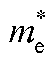
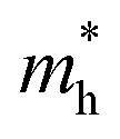
All the calculations in this paper are based on Density Functional Theory (DFT) and the Projector-Augmented-Wave (PAW) method,22 and were carried out using the VASP (Vienna Ab initio Simulation Package)23 software package. To obtain accurate calculation results, the cutoff energy is set to 520 eV, the self-consistent field (SCF) convergence accuracy is 2 × 10⁻⁶ eV per atom, and the k-points in the first Brillouin zone are sampled using a 3 × 3 × 1 Monkhorst–Pack grid. To avoid the interaction between adjacent supercells along the interlayer, a vacuum layer of 18 Å was added in the out-of-plane vertical direction for the four groups of heterojunction structures. Geometric optimization was carried out using the BFGS algorithm, and van der Waals forces were taken into account with the Tkatchenko–Scheffler (TS) dispersion correction.24 All calculations were performed in reciprocal lattice vector space. In addition, the stability of the heterojunction system was tested using the ab initio molecular dynamics (AIMD). The AIMD test based on DFT used the Nosé–Hoover thermostat to control the temperature, with a total simulation length of 8000 steps and a time step of 0.8 fs.2.2 Model construction
This paper studies the relatively stable ideal ZnO crystal, whose stable phase is hexagonal wurtzite and belongs to the P63mc space group, with unit cell parameters of α = β = 90° and γ = 120°. The chalcogenide compounds MoS2 and MoSe2 belong to the P63/mmc space group, and the stable phase of these two structures is the 2H phase, which exhibits semiconductor properties. The 2H phase adopts an ABA stacking mode, that is, the sulfur atoms in the upper layer are directly above those in the lower layer. WS2 and WSe2 are characterized by the periodic arrangement of metal and chalcogen elements in a hexagonal structure. However, this hexagonal structure differs from that of graphene. When observed along the c-axis, the structural arrangement in the system forms an X–M–X sandwich.The ZnO unit cell was expanded by 3 × 3 × 1, and a single layer was cut along the (001) plane. The optimized model is shown in Fig. 1(a). The band structure of the single-layer ZnO was calculated using both the Perdew–Burke–Ernzerhof (PBE)25 functional and the hybrid functional Heyd–Scuseria–Ernzerhof (HSE06).26 The band gap calculated using the HSE06 hybrid functional is 3.32 eV (as shown in Fig. 1(a)), and the error compared to the experimental results is only 0.602%.27 This value is closer to the actual result than that obtained using PBE (as shown in Fig. 1(b)). Consequently, all subsequent calculations in this work will employ the HSE06 method. According to Fig. 2, the optimal interlayer distances of ZnO–MX2 are 3.401 Å, 2.966 Å, 3.302 Å, and 2.808 Å, respectively.
 | ||
| Fig. 1 (a) Crystal model of single-layer ZnO; (b) band structure calculated by PBE; and (c) band structure calculated by HSE06. | ||
 | ||
| Fig. 2 Layer spacing optimization test diagram (a) ZnO–MoSe2 (b) ZnO–WSe2 (c) ZnO–MoS2 (d) ZnO–WS2. | ||
3. Analysis and discussion
3.1 Stability analysis
| σ = (a2 − a1)/a1 | (1) |
| Heterojunction | ZnO–MoSe2 | ZnO–WSe2 | ZnO–MoS2 | ZnO–WS2 |
|---|---|---|---|---|
| d (Å) | 3.401 | 2.966 | 3.302 | 2.088 |
| σ (%) | 2.11 | 1.01 | 2.17 | 2.12 |
| Eb (eV) | −7.20 | −7.56 | −6.99 | −6.94 |
| Eg (eV) PBE | 1.129 | 1.421 | 0.235 | 1.420 |
| Eg (eV) HSE06 | 1.956 | 2.098 | 1.014 | 1.493 |
To further discuss the structural stability, the binding energy of ZnO–MX2 was also calculated. When Eb is negative, the larger its absolute value, the higher the stability of the system. The interface binding energy can be expressed as follows:30
| Eb = EZnO–MX2 − EZnO − EMX2 | (2) |
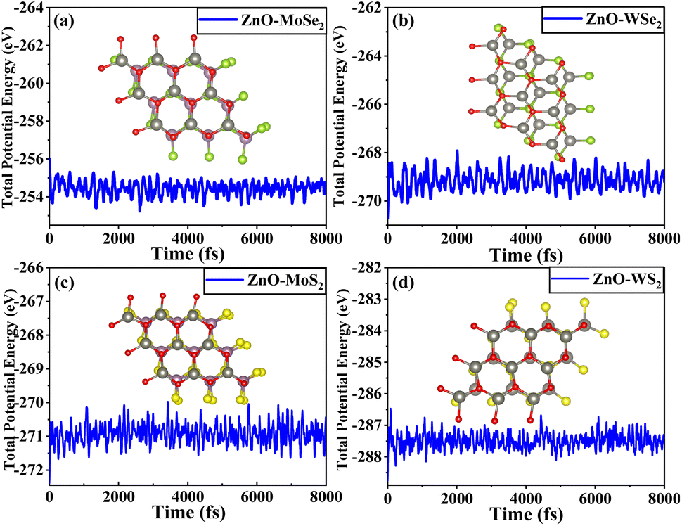 | ||
| Fig. 3 AIMD curves of total energy and temperature of (a) ZnO–MoSe2 (b) ZnO–WSe2 (c) ZnO–MoS2 (d) ZnO–WS2 (the inset shows the top views of the four heterojunctions). | ||
3.2 Electronic structure
 | ||
| Fig. 4 (a and b) Show the band structure (left) and density of states (right) of ZnO–MoSe2, (c and d) of ZnO–WSe2, (e and f) of ZnO–MoS2, and (g and h) of ZnO–WS2. (In the figure, the contribution of each atom is represented by the size of the small balls. The larger the ball, the greater the contribution of the corresponding atom.) | ||
Fig. 4(c) and (d) respectively show the band structure and electron density diagram of ZnO–WSe2, with a band gap of 2.098 eV. Compared to bulk ZnO, the band gap of this system is reduced; the conduction band position is significantly lowered, and the energy levels are more densely packed. It is a direct transition type. Electrons require less energy to transition from the top of the valence band to the bottom of the conduction band, leading to a redshift in the absorption edge and a significant enhancement in the response to visible light. From the analysis of the TDOS diagram, it can be seen that the CBM and VBM of this system are both contributed by WSe2, indicating a type I band alignment. Under light irradiation, the photogenerated electron–hole pairs tend to accumulate in the WSe2 layer, making effective separation challenging. The analysis of the DOS in the valence band and conduction band indicates that the CBM of the ZnO–WSe2 is primarily composed of the W-5d states in WSe2, while the VBM is mainly contributed by the O-2p states in ZnO and the W-5d states in WSe2, with a minor contribution from the Zn-3d states in ZnO. In addition, a new peak emerged on the right side of the Fermi level, mainly contributed by the N-2p state, indicating that some energy levels split. This is manifested as a sparser energy level distribution in the band diagram. At 5.25 eV, the electronic orbitals of WSe2 and ZnO overlap, which is conducive to electron transfer.
It can be seen from Fig. 4(e) and (f) that the band gap of ZnO–MoS2 is 1.014 eV, and the transition mode is direct. The conduction band as a whole shifts downward, and the energy levels become more densely packed, indicating that the number of electrons that can be accommodated in this energy region increases, that is, the electron density in the system increases, leading to a higher transition probability and significantly improved photocatalytic efficiency. Furthermore, the CBM of this system is contributed by the MoS2, while the VBM is contributed by the ZnO, indicating that it belongs to a type II heterojunction. From the TDOS diagram analysis, it is evident that MoS2 plays a decisive role in determining the CBM and VBM. From the partial wave density of states analysis, it can be seen that the CBM of this system is primarily contributed by the Mo-4d and S-3p states in MoS2, while the VBM is mainly composed of the Mo-4d and S-3p states in MoS2 as well as the O-2p states in ZnO. The Mo-4d and S-3p electron orbitals fully overlap, and the electrons between different layers hybridize, thereby generating an internal electric field within the system that facilitates the transition of photogenerated carriers, thus improving both the injection efficiency and the charge flow rate. The above analysis indicates that the photocatalytic performance of this system has been significantly improved.
Fig. 4(g) and (h) respectively show the band structure and electronic density of states of the ZnO–WS2. The band gap of this system is 1.493 eV. Compared with the single-layer ZnO (see Fig. 1(b)), the conduction band position shifts downward, the band gap narrows, and the energy levels become more dense, indicating a direct transition type. Its CBM is mainly contributed by the WS2, while the VBM is mainly contributed by the ZnO, which belongs to the type II band alignment. From the DOS diagram analysis, it can be seen that the conduction band is primarily contributed by WS2, while the valence band is jointly composed of ZnO and WS2. The wave function-resolved DOS analysis indicates that the VBM of the ZnO–WS2 is mainly provided by the W-5d state in WS2 and the O-2p state in ZnO, with minor contributions from the W-6s state in WS2 and the Zn-4s state in ZnO; meanwhile, the CBM is predominantly provided by the W-5d state in WS2. The CBM of this system originates from WS2, and the VBM originates from ZnO, forming a type II heterojunction, which is consistent with the band structure diagram. This process significantly enhances electron migration efficiency, thereby effectively boosting the photocatalytic activity of the entire system.
Overall, the ZnO–MoSe2 and ZnO–WSe2 are type I heterojunctions. The photogenerated electrons transfer from the CBM of ZnO to the CBM of MoSe2 and WSe2. This band structure is conducive to the rapid recombination of photogenerated carriers, and thus is mainly applied in the field of light-emitting devices such as LEDs and photovoltaic cells. Meanwhile, ZnO–MoS2 and ZnO–WS2 belong to type II heterojunctions, with their energy bands arranged in an offset manner. This causes the photogenerated electrons and holes to accumulate in different materials, respectively, effectively suppressing the recombination of photogenerated carriers and promoting carrier separation. This type of heterojunction is mainly applied in fields such as photocatalysis and photodetection. For instance, in the process of photocatalytic water splitting for hydrogen production, it can significantly enhance the separation efficiency of photogenerated electron–hole pairs, thereby increasing the overall efficiency of the photocatalytic reaction.
| Δρ = ρ(ZnO/MX2) − ρ(ZnO) − ρ(MX2) | (3) |
| Φ = Evac − EFermi | (4) |
 | ||
| Fig. 5 Presents the planar average electrostatic potential diagrams of (a) ZnO–MoSe2, (b) ZnO–WSe2, (c) ZnO–MoS2, and (d) ZnO–WS2. The inset figures illustrate the side views of the three-dimensional differential charge density (yellow indicates electron accumulation, while cyan indicates depletion). Panels (e) ZnO–MoSe2, (f) ZnO–WSe2, (g) ZnO–MoS2, and (h) ZnO–WS2 depict the work function diagrams, with the inset figures showing the side views of the corresponding single-layer system models. | ||
 and holes
 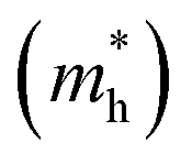 in the ZnO–MX2 as well as their ratio (D) to evaluate the retention of electrons and holes in the system after absorbing light. The formula for effective mass is given by:34
 | (5) |
The unit of (∂2E/∂K2) is (2π/a)2 eV, where ħ = h/2π. A higher D value indicates a greater difference in the effective masses of electrons and holes in the system. Although D is not a direct criterion for the recombination rate, it provides a way to determine whether the photogenerated electrons and holes can be utilized in the photocatalytic water splitting process. As shown in Table 2, the effective mass of holes in all systems is greater than that of electrons, forming a heavy-hole–light-electron system. This further suggests that electrons and holes within the system can be effectively separated.
| Systems | ZnO | ZnO–MoSe2 | ZnO–WSe2 | ZnO–MoS2 | ZnO–WS2 |
|---|---|---|---|---|---|
 |
0.31 | 0.32 | 0.36 | 0.27 | 0.31 |
 |
0.19 | 0.40 | 0.43 | 0.36 | 0.48 |
D  |
0.61 | 1.25 | 1.13 | 1.33 | 1.55 |
The effective electron mass  of the ZnO–MoS2 is slightly larger than that of monolayer ZnO due to the contribution of the S-3s state in the conduction band. Compared with monolayer ZnO, the effective hole mass in the heterojunction system has increased. In the ZnO–WSe2, the D value is closest to 1, indicating that the electron and hole mobilities are not significantly different. This suggests that this system may not be very suitable for use as a photocatalyst. Compared with the literature, the errors in the effective masses of electrons and holes calculated in this paper are 5% and 4%, respectively, indicating that the calculation results of this paper have reference value.35 Compared with ZnO, the D value of the ZnO–MX2 significantly increases, indicating that after constructing the heterojunction, the recombination rate of photogenerated electrons and holes in the system decreases, thereby effectively enhancing the photocatalytic efficiency of the material. Among them, the D value of the ZnO–WS2 is the highest, meaning that the separation of electrons and holes in this system is most pronounced, making it less likely for them to recombine and facilitating further separation of photogenerated carriers.
The D values of ZnO–MS2 are greater than those of ZnO–MSe2, suggesting a more prominent separation of electrons and holes in ZnO–MS2. This phenomenon reduces the probability of carrier recombination and promotes the further separation of photogenerated carriers. This finding is consistent with the characteristic of ZnO–MS2 forming a type-II heterojunction, which effectively enhances the separation of electron–hole pairs.
3.3 Optical properties
The magnitude of the dielectric function reflects the strength of a medium's ability to bind charges. The larger the magnitude of the dielectric function, the stronger the material's response to an electric field and the greater its polarization capacity. From the real part of the dielectric function graph in Fig. 6(a), it can be seen that the static dielectric constants of the five systems, ZnO, ZnO–MoSe2, ZnO–WSe2, ZnO–MoS2, and ZnO–WS2, are 2.32, 1.77, 4.93, 1.98, and 5.72, respectively. By comparison, it can be seen that the static dielectric constant value of the ZnO–WS2 is the largest, indicating a higher number of electric dipoles in this system, which can maximize the carrier density and the efficiency of charge transport and separation. In the visible light range around 2 eV, both the ZnO–WS2 and ZnO–WSe2 exhibit a prominent and sharp peak, indicating that these two heterojunctions have a stronger response to light and a greater polarization capacity.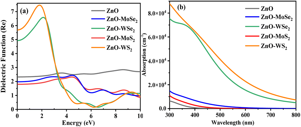 | ||
| Fig. 6 Optical property spectra of ZnO-based heterojunctions: (a) real part of the dielectric function; (b) absorption spectrum. | ||
As shown in Fig. 6(b), the absorption edge of ZnO is approximately at 430 nm, and its light absorption intensity gradually decreases within the range of 450 to 800 nm, with almost no obvious absorption peak. The absorption peaks of the four heterojunctions are all significantly higher than that of ZnO, with the absorption band edges redshifted and shifted towards the low-energy region. The intensity of light absorption shows an upward trend. At approximately 5.32 eV, the light absorption peaks of the four systems overlap, indicating that the light absorption intensity reaches its maximum at this energy level.
The above results are due to the fact that, compared to the ZnO2 monolayer, the band gaps of all heterojunctions exhibit a decreasing trend, which correspondingly reduces the minimum photon energy required for electron transitions. This enables the material to absorb photons with longer wavelengths (i.e., lower energy) – for example, extending the absorption range from ultraviolet light to visible light or even infrared light – thereby effectively broadening the spectral range of light absorption. Additionally, the built-in electric field present in the heterojunction accelerates the transition process of photo-generated electrons through the action of the electric field force. Therefore, under the synergistic effect of the reduced band gap and the built-in electric field, the absorption coefficients of all four systems are significantly enhanced, and their absorption spectra all exhibit redshift phenomena.
Among them, the absorption peaks of ZnO–WS2 and ZnO–WSe2 are significantly higher than those of ZnO–MoS2 and ZnO–MoSe2, indicating that the former two have higher light absorption intensities. The energy range corresponding to visible light is 1.61 to 3.10 eV. Within this range, ZnO–WS2 and ZnO–WSe2 exhibit the best light absorption performance, especially the ZnO–WSe2, which has the highest light absorption rate. Corresponding to Fig. 6(a), the light absorption effect of ZnO–WS2 and ZnO–WSe2 is significantly better than that of ZnO–MoS2 and ZnO–MoSe2.
3.4 Photocatalytic performance
The position of the band edge is one of the core elements for evaluating the performance of a photocatalyst. An ideal photocatalyst should have a band gap that covers the redox potential of water, meaning that the conduction band minimum of the material should be lower than the reduction potential of H+/H2, while the valence band maximum should be higher than the oxidation potential of O2/H2O.36 This requirement is crucial for the design and selection of efficient photocatalysts, as it not only directly affects the efficiency of photocatalytic water splitting but also determines the stability and service life of the photocatalyst. Based on the concept of semiconductor electronegativity, this paper calculates the oxidation–reduction potential of each system relative to water, with the specific expression given in ref. 37.| EVBM = χ − Eelec + 0.5Eg | (6) |
| ECBM = EVBM − Eg | (7) |
| Heterojunction | ZnO–MoSe2 | ZnO–WSe2 | ZnO–MoS2 | ZnO–WS2 |
|---|---|---|---|---|
| ECBM (eV) | −0.214 | −0.165 | 0.7532 | −0.051 |
| EVBM (eV) | 2.169 | 2.263 | 1.7671 | 1.442 |
 | ||
| Fig. 7 Shows the oxidation–reduction band edge positions of ZnO monolayer and ZnO–MX2 heterojunctions (under the condition of pH = 0, with the oxidation–reduction potential of H+/H2 and O2/H2O). | ||
As shown in Fig. 7, after constructing ZnO-based heterojunctions, their band gaps are significantly reduced and become closer to the redox potential of water, indicating that constructing ZnO-based heterojunctions is an effective strategy to enhance their photocatalytic performance.38
Comparing the two types of type-I heterojunctions, ZnO–MoSe2 and ZnO–WSe2, although their CBMs are both higher than the reduction potential and their VBMs are both lower than the oxidation potential, meeting the basic conditions for redox reactions to occur, it is observed that both electrons and holes mainly migrate from the ZnO layer to the MoSe2 or WSe2 layers, resulting in difficulty in achieving effective separation of charge carriers. Therefore, such structures are not well-suited to serve as efficient photocatalysts.
It is observed in the two types of type-II heterojunctions, ZnO–MoS2 and ZnO–WS2, that both exhibit alternating band structures. Specifically, electrons accumulate in the MoS2/WS2 layer, while holes accumulate in the ZnO layer. This electron transfer mechanism helps achieve effective separation of electron–hole pairs, thereby promoting more electrons to participate in redox reactions and significantly enhancing photocatalytic performance.39,40
In the ZnO–MoS2, the CBM of MoS2 is located below the H+/H2 reduction potential, thereby rendering the photocatalyst incapable of hydrogen production. The VBM of ZnO–MoS2 lies above the O2/H2O oxidation potential, thereby enabling the ZnO–MoS2 system to satisfy the requirements for the oxygen evolution reaction. On the contrary, in ZnO–WS2, the CBM and VBM are respectively located on the upper and lower sides of the redox potential. Thus, it can be concluded that ZnO–WS2, as a photocatalyst, is capable of facilitating both HER and OER.
4. Conclusion
The ZnO–MX2 (M = Mo, W; X = S, Se) heterojunctions exhibit excellent structural stability. The AIMD simulation results show that they have the smallest energy fluctuation amplitude at 300 K. Specifically, the band gaps of ZnO–MoSe2 (1.956 eV), ZnO–WSe2 (2.098 eV), ZnO–MoS2 (1.014 eV) and ZnO–WS2 (1.493 eV) are significantly smaller than that of single-layer ZnO, enabling them to effectively absorb visible light. The electron transfer from MX2 to ZnO constructs an internal electric field pointing to MX2 at the interface, further enhancing the charge separation efficiency.ZnO–MS2 systems form type-II heterojunctions, whereas ZnO–MSe2 systems form type-I heterojunctions. The D values of ZnO–MS2 are larger than those of ZnO–MSe2, indicating that the separation of electrons and holes in ZnO–MS2 is more pronounced. This reduces the likelihood of recombination and facilitates the further separation of photogenerated carriers. This conclusion aligns with the characteristic of ZnO–MS2 forming a type-II heterojunction, which enhances the separation of electron–hole pairs.
The static dielectric constants of ZnO–MS2 systems are greater than that of ZnO–MSe2 systems, indicating that ZnO–MS2 systems have better internal field polarization ability, which is highly conducive to the separation of electron–hole pairs. All four heterojunctions exhibit a distinct redshift in the absorption spectrum, among which the absorption coefficient of ZnO–MS2 systems is greater than that of ZnO–MSe2 systems.
It can be inferred from the analysis that type-I heterojunctions (ZnO–MoSe2/WSe2) exhibit inefficient charge separation. In contrast, type-II heterojunctions demonstrate enhanced functionality, as ZnO–MoS2 promotes oxygen evolution but not hydrogen evolution. Moreover, the bandgap of ZnO–WS2 straddles the water's redox potentials, indicating that ZnO–WS2 effectively promotes both OER and HER.
Overall, ZnO–WS2 emerges as the most promising photocatalyst due to its optimal charge separation, exceptional light absorption, and superior dielectric properties. This work provides critical insights for designing high-performance ZnO-based heterostructures through bandgap engineering and interfacial charge regulation.
Data availability
This study did not generate any new datasets. All data analyzed are from publicly available sources, as cited in the manuscript.Conflicts of interest
The authors declare that they have no known competing financial interests or personal relationships that could have potentially influenced the work reported in this paper.Acknowledgements
This study was supported by Xinjiang Yili Normal University Discipline Comprehensive Strength Enhancement Special Project (22XKZZ24); and Science and Technology Project of Xinjiang Yili Kazak Autonomous Prefecture (YZ2022B021).References
- D. Zheng, Y. Xue, J. Wang, P. S. Varbanov, J. J. Klemeš and C. Yin, Nanocatalysts in photocatalytic water splitting for green hydrogen generation: Challenges and opportunities, J. Cleaner Prod., 2023, 414(33), 137700 Search PubMed.
- Y. Dong, Y. Zhang and S. Liu, The impacts and instruments of energy transition regulations on environmental pollution, Environ. Impact Assess. Rev., 2024, 105(2), 107448 Search PubMed.
- P. Zhou, I. A. Navid, Y. Ma, Y. Xiao, P. Wang, Z. Ye, B. Zhou, K. Sun and Z. Mi, Solar-to-hydrogen efficiency of more than 9% in photocatalytic water splitting, Nature, 2023, 613(7942), 66–70 Search PubMed.
- A. S. Shuaibu, H. Y. Hafeez, J. Mohammed, U. M. Dankawu, C. E. Ndikilar and A. B. Suleiman, Progress on g-C3N4 based heterojunction photocatalyst for H2 production via Photocatalytic water splitting, J. Alloys Compd., 2024, 1002(33), 175062 CrossRef CAS.
- J. Fu, K. Jiang, X. Qiu, J. Yu and M. Liu, Product selectivity of photocatalytic CO2 reduction reactions, Mater. Today, 2020, 32(1), 222–243 CrossRef CAS.
- X. Zhang, S. Zhang, K. Mathivanan, R. Zhang, J. Zhang, Q. Jiang, W. Sand, J. Duan and B. Hou, Research progress and prospects in antifouling performance of photocatalytic sterilization: A review, J. Mater. Sci. Technol., 2025, 208(5), 189–201 CrossRef CAS.
- I. Ahmad, Y. Zou, J. Yan, Y. Liu, S. Shukrullah, M. Y. Naz, H. Hussain, W. Q. Khan and N. R. Khalid, Semiconductor photocatalysts: A critical review highlighting the various strategies to boost the photocatalytic performances for diverse applications, Adv. Colloid Interface Sci., 2023, 311(1), 102830 CrossRef CAS PubMed.
- Y. Ying, K. Fan, Z. Lin and H. Huang, Facing the “Cutting Edge:” Edge Site Engineering on 2D Materials for Electrocatalysis and Photocatalysis, Adv. Mater., 2025, 37(10), 2418757 CrossRef CAS.
- Y. Tang, Y. Lu, B. Ma, J. Song, L. Bai, Y. Wang, Y. Chen and M. Liu, Rational Design of ZnO/Sc2CF2 Heterostructure with Tunable Electronic Structure for Water Splitting: A First-Principles Study, Molecules, 2024, 29(19), 4638 CrossRef CAS PubMed.
- P. Dhiman, G. Rana, A. Kumar, G. Sharma, D.-V. N. Vo and Mu. Naushad, ZnO-based heterostructures as photocatalysts for hydrogen generation and depollution: a review, Environ. Chem. Lett., 2022, 20(2), 1047–1081 CrossRef CAS.
- G. Wang, H. Yuan, J. Chang, B. Wang, A. Kuang and H. Chen, One-step in-situ construction engineering of ZnO-Zn2SnO4 heterojunction for deeply photocatalytic oxidation of nitric oxide, J. Colloid Interface Sci., 2024, 664(12), 433–443 Search PubMed.
- R. Yang, Y. Fan, Y. Zhang, L. Mei, R. Zhu, J. Qin, J. Hu, Z. Chen, Y. Hau Ng and D. Voiry, et al, 2D Transition Metal Dichalcogenides for Photocatalysis, Angew. Chem., Int. Ed., 2023, 62(13), e202218016 CrossRef CAS.
- J. Tao, L. Huang, S. Xiong, L.-X. Li, L.-L. Wang and L. Xu, Two-dimensional TMDs/MN (M = Al, Ga) van der Waals heterojunction photocatalyst: a first-principles study, J. Mater. Sci., 2023, 58(35), 14080–14095 CrossRef CAS.
- Y. Jin, M. Jin, J. Bai, J. Li, Z. Wu, Z. Li, J. Xiang and C. Guo, Mechanism analysis of photocatalytic activity on Semiconductor-Type-Modulated heterojunctions, Appl. Surf. Sci., 2024, 656(15), 159683 CrossRef CAS.
- M. Haddad, A. Belhadi, L. Boudjellal and M. Trari, Photocatalytic hydrogen production on the hetero-junction CuO/ZnO, Int. J. Hydrogen Energy, 2021, 46(75), 37556–37563 CrossRef CAS.
- H. Li, R. Wu, J. Ji, Y. Liu, J. Zhao, S. Sahar and A. Zeb, Efficient CeO2/ZnO heterojunction for enhanced heterogeneous photocatalytic application, Inorg. Chem. Commun., 2025, 171(1), 113553 CrossRef CAS.
- X. Yuan, M. Wu, J. Ni, Y. Cheng and C. Ni, Tuning the ZnO/GaN heterojunction for atmospheric NO abatement, Appl. Surf. Sci., 2023, 635(29), 157712 CrossRef CAS.
- G. Jia, Y. Zhang and P. Wang, Nano-photo-thermal energy drive MoS2/ZnO nanoheterojunctions growing, Opt. Mater. Express, 2016, 6(3), 876–883 CrossRef CAS.
- G. Jiang, C. Yao, Z. Wang, X. Wang and Y. Cai, Semiconducting ZnO & WS2 heterojunction composite films: Fabrication, characterization and ultrafast nonlinear properties, J. Alloys Compd., 2021, 863(14), 158664 CrossRef CAS.
- Y. Guan and Y. Du, Two-dimensional ZnO/MoSe2 van der Waals heterostructure used as promising photocatalyst for water splitting: A DFT study, Chem. Phys. Lett., 2022, 803(18), 139828 CAS.
- G. Wang, H. Yuan, J. Chang, B. Wang, A. Kuang and H. Chen, ZnO/MoX2 (X = S, Se) composites used for visible light photocatalysis, RSC Adv., 2018, 8(20), 10828–10835 RSC.
- A. S. Oreshonkov, Electronic transitions and vibrational properties of bulk and monolayer g-C3N4, and a g-C3N4/MoS2 heterostructure from a DFT study, Phys. Chem. Chem. Phys., 2024, 26(35), 23023–23031 RSC.
- X. Zhang, 1 D CeO2/g-C3N4 type II heterojunction for visible-light-driven photocatalytic hydrogen evolution, Inorg. Chem. Commun., 2022, 144(10), 109838 CrossRef CAS.
- L. Luan, L. Han, D. Zhang, K. Bai, K. Sun, C. Xu, L. Li and L. Duan, AlSb/ZrS2 heterojunction: A direct Z-scheme photocatalyst with high solar to hydrogen conversion efficiency and catalytic activity across entire PH range, Int. J. Hydrogen Energy, 2024, 51(3), 1242–1255 CrossRef CAS.
- Z.-L. Liu, R.-R. Liu, Y.-F. Mu, Y.-X. Feng, G.-X. Dong, M. Zhang and T.-B. Lu, In Situ Construction of Lead-Free Perovskite Direct Z-Scheme Heterojunction Cs3Bi2I9/Bi2WO6 for Efficient Photocatalysis of CO2 Reduction, Sol. RRL, 2021, 5(3), 2000691 CrossRef CAS.
- Y. Zhang, Z. Qiang, J. Ding, K. Xie, L. Duan and L. Ni, First-principles prediction of a direct Z-scheme WSe2/HfS2 van der Waals heterostructure for overall photocatalytic water decomposition, CrystEngComm, 2024, 26(60), 2621–2634 RSC.
- Y. Zhang, W. Yang, Z. Zhu, L. Zhang and W. Peng, Temperature-Sensitive Template for Preparation of ZnO/CeO2 Composite Photocatalytic Materials and Its Catalytic Performance, Molecules, 2024, 29(15), 3589 CrossRef CAS PubMed.
- J. Wang, Y. Sun, J. Lai, R. Pan, Y. Fan, X. Wu, M. Ou, Y. Zhu, L. Fu, F. Shi and Y. Wu, Two-dimensional graphitic carbon nitride/N-doped carbon with a direct Z-scheme heterojunction for photocatalytic generation of hydrogen, Nanoscale Adv., 2021, 3(23), 6580–6586 RSC.
- K. Tian, G. Qian, Q. Liu, X. Fu, S. Zhang, Q. Xie and X. Luo, Direct Z-scheme GeC/GaSe heterojunction by first-principles study for photocatalytic water splitting, Mater. Sci. Semicond. Process., 2024, 184(16), 108855 CrossRef CAS.
- Y. Liu, Y. Yao, Z. Liang, Z. Gong, J. Li, Z. Tang and X. Wei, Two-Dimensional AlN/PtSSe Heterojunction as A Direct Z-Scheme Photocatalyst for Overall Water Splitting: A DFT Study, J. Phys. Chem. C, 2024, 128(24), 9894–9903 CrossRef CAS.
- N. Jaykhedkar, R. Bystrický, M. Sýkora and T. Bučko, How the Temperature and Composition Govern the Structure and Band Gap of Zr-Based Chalcogenide Perovskites: Insights from ML Accelerated AIMD, Inorg. Chem., 2023, 62(31), 12480–12492 CrossRef CAS.
- C. Zhao, Z. Li and Z. Zhang, Stable WSeTe/PtTe2 van der Waals heterojunction: Excellent mechanical, electronic, and optical properties and device applications, Appl. Surf. Sci., 2024, 672(31), 160859 CrossRef CAS.
- K. Si, J. Ma, C. Lu, Y. Zhou, C. He, D. Yang, X. Wang and X. Xu, A two-dimensional MoS2/WSe2 van der Waals heterostructure for enhanced photoelectric performance, Appl. Surf. Sci., 2020, 507(9), 145082 CrossRef CAS.
- I. Ahmad, S. Shukrullah, M. Yasin Naz, S. Ullah and M. Ali Assiri, Designing and modification of bismuth oxyhalides BiOX (X = Cl, Br and I) photocatalysts for improved photocatalytic performance, J. Ind. Eng. Chem., 2022, 105(1), 1–33 CAS.
- F. Hu, L. Tao, H. Ye, X. Li and X. Chen, ZnO/WSe2 vdW heterostructure for photocatalytic water splitting, J. Mater. Chem. C, 2019, 7(23), 7104–7113 RSC.
- A. Bao, Y. Ma, X. Guo, J. Wang, Y. Zhao, Z. Liu, Y. Wang, X. Liu and Y. Zhang, Tunable electronic and optical properties of a type-II GaP/SiH van der Waals heterostructure as photocatalyst: A first-principles study, Int. J. Hydrogen Energy, 2024, 88(28), 1256–1266 CrossRef CAS.
- Z.-N. Dai, Y. Xu, D. F. Zou, W. J. Yin and J. N. Wang, InN/XS2 (X = Zr, Hf) vdW heterojunctions: promising Z-scheme systems with high hydrogen evolution activity for photocatalytic water splitting, Phys. Chem. Chem. Phys., 2023, 25(11), 8144–8152 RSC.
- I. Ahmad, R. Bousbih, A. Mahal, W. Q. Khan, M. Aljohani, M. A. Amin, N. N. A. Jafar, M. S. Jabir, H. Majdi, A. S. Alshomrany, M. Shaban, I. Ali and H. Bayahia, Recent progress in ZnO-based heterostructured photocatalysts: A review, Mater. Sci. Semicond. Process., 2024, 180(12), 108578 CrossRef CAS.
- Q. Fan, Z. Yan, J. Li, X. Xiong, K. Li, G. Dai, Y. Jin and C. Wu, Interfacial-electric-field guiding design of a Type I FeIn2S4@ZnIn2S4 heterojunction with ohmic-like charge transfer mechanism for highly efficient solar H2 evolution, Appl. Surf. Sci., 2024, 663(22), 160206 CrossRef CAS.
- X. T. Zhu, Y. Xu, Y. Cao, Y. Q. Zhao, W. Sheng, G.-Z. Nie and Z. Ao, Investigation of the electronic structure of two-dimensional GaN/Zr2CO2 hetero-junction: Type-II band alignment with tunable band gap, Appl. Surf. Sci., 2021, 542(8), 148505 Search PubMed.
| This journal is © The Royal Society of Chemistry 2025 |