
 Open Access Article
 This Open Access Article is licensed under a Creative Commons Attribution-Non Commercial 3.0 Unported Licence
Optoelectronic applications of chemical bath deposited Cu2SnS3 (CTS) thin films†
Jolly B. Raval *a,
Sunil H. Chaki*b,
Jiten P. Tailorc,
Sandip V. Bhattb,
Sefali R. Patele,
Rahul K. Desaid,
Bishwajit S. Chakrabartyd and
Milind P. Deshpandea
*a,
Sunil H. Chaki*b,
Jiten P. Tailorc,
Sandip V. Bhattb,
Sefali R. Patele,
Rahul K. Desaid,
Bishwajit S. Chakrabartyd and
Milind P. Deshpandea
aP.G. Department of Physics, Sardar Patel University, Vallabh Vidyanagar, Gujarat – 388120, India. E-mail: ravaljolly48@spuvvn.edu
bDepartment of Physics, M.B. Patel Science College, Anand, Gujarat – 388001, India. E-mail: sunil_chaki@spuvvn.edu
cDepartment of Applied & Interdisciplinary Sciences, CISST, Sardar Patel University, Vallabh Vidyanagar, Gujarat – 388120, India
dDepartment of Applied Physics, Faculty of Technology and Engineering, M.S. University of Baroda, Vadodara, Gujarat, India
eDepartment of Physics, Veer Narmad South Gujarat University, Surat, Gujarat-395007, India
First published on 11th July 2025
Abstract
Cu2SnS3 (CTS) thin film (TF) is deposited by a low-cost chemical bath deposition method. The wurtzite unit cell structure of deposited CTS TF is confirmed by X-ray diffraction analysis. The atomic force microscopy shows uniform and defect-free deposition of CTS TF. The direct optical bandgap of 1.48 eV is confirmed by diffuse reflectance spectroscopy. The deposited CTS TF is studied for photo-response properties. Responsivity, sensitivity, and detectivity of 5.73 mW A−1, 114.27 × 10⁻³, and 6.39 × 10¹² Jones are obtained respectively. In another application, the first ever heterojunction and a photo-electrochemical (PEC) type CTS-TiO2 configuration within a single solar cell device is carried out. This CTS-TiO2 based combined solar cell delivered a current density of 0.05 mA cm−2, open circuit voltage of 0.47 V, efficiency of 0.014%, and fill factor of 0.63. Theoretical predictions of solar cell parameters for the CTS-CdX (X = S, Se) heterojunction device are carried out using SCAPS-1D simulation. Temperature-dependent thickness variations at 273, 298, 310, and 373 K are carried out to evaluate the device performance. The obtained results are discussed in detail.
1. Introduction
Quenching for renewable energy sources and finding their alternatives has become a necessity these days. The global energy crisis, such as lack of elements from the earth crust, overuse of coal and minerals, overdependence on established resources, air–water–land pollution, shortage of water, etc., are leading researchers to extract better alternatives using different approaches. These alternatives involve various trendy materials that are available in different forms, such as nanoparticles (NP), thin films (TFs), single/polycrystals, etc. Utilization of these forms can find their practical applications in photovoltaics,1 photocatalysts,2 environmental and biosensors,3,4 visible and infrared photodetectors,5,6 etc. Among them, TF solar cell technology has proven to be a better substitute than the other mentioned forms.7 The 1st generation silicon-based solar cells are extensively utilized in photovoltaic industries but some of the disadvantages that need to be addressed are indirect bandgap, high operating temperature, and time-worn use.8,9 In the direction of addressing this, TFs of various new binary, ternary, and quaternary materials with tremendous properties are introduced every year. Conventional copper–indium–gallium–sulfur and binary cadmium-, lead-, and zinc-based chalcogenides played key role for setting directions and deliver efficient photovoltaic properties.10 Other ternary materials such as Cu2Sn(S,Se)3,11,12 CuFe(S,Se)2,13,14 CuSb(S,Se)2,15,16 etc., are extensively synthesized due to their salient properties such as p-type conductivity,17 high absorption coefficient,18 significant charge carrier concentration,19 appropriate bandgap range which is suitable for solar cells.20 In copper-based ternary chalcogenides, Cu2SnS3 (CTS) is primarily employed as a p-type layer in photovoltaics because of its excellent properties such as, alterable bandgap range between 0.96 to 1.75 eV,21 high carrier concentration,22 existence of various crystal structures,23 excellent electrical and thermal conductivity,24,25 high figure of merit (ZT) and Seebeck coefficient.26,27 Experimentally, the CTS TFs are deposited by various physical and chemical methods such as sputtering,28 spin/dip coatings,29,30 pulsed laser deposition,31 thermal evaporation,32 chemical bath deposition,33 etc. As far as photovoltaic applications of CTS TFs are concerned, Nakshima et al.34 reported solar cell efficiency (η), open circuit voltage (VOC), current density (JSC) and fill factor (FF) of 4.63%, 283 mV, 37.3 mA cm−2 and 0.439% respectively by utilizing sequential evaporation method. Kanai et al.35 reported maximum η, VOC, JSC and FF of 5.24%, 0.25 V, 40.2 mA cm−2 and 0.52 respectively. As far as theoretical predictions about these solar cell parameters are concerned, the use of SCAPS-1D software is extensively utilized these days. The software allows various parametric simulations based on material's bandgap, thickness, donor and acceptor density, electron and hole thermal velocity, and electron and hole mobility,36 etc. In literature, various simulations, such as basic p–n junctions, sandwiching a perovskite layer and heterojunctions with various buffer layers with p-type CTS, demonstrated maximum predictable efficiency up to 32%.21,37–41 As far as the n-type layer is concerned, CdS is majorly employed due to the conduction band offset of −0.1 to 0.4 eV,42 optical bandgap of ∼2.4 eV,43–45 stability against photo-anodic dissolution,46 delivering efficiency in heterojunction solar cells greater than 10%,47 tunable size and thickness in case of NPs and TFs respectively,48,49 low resistivity,50 etc. The other cadmium based chalcogenide that is widely employed is CdSe due to its n-type conductivity,51 having direct bandgap of ∼1.71 eV,52 higher capacity of photon absorption in the visible range,53 high absorption coefficient of ∼104 cm−1,54 higher conduction band edge,55 etc. By selecting the right p- and n-type layers for these simulations will not only deliver high theoretical device efficiency but also paves the way for experimental advancements.In this work, the CTS TF is deposited on an FTO substrate via the chemical bath deposition (CBD) technique. Comprehensive characterization using X-ray diffraction (XRD), diffuse reflectance spectroscopy (DRS), and atomic force microscopy (AFM) confirmed the film's structural and optical attributes. To evaluate its multifunctional applicability, three experimental applications are employed. Initially, the photo-response behavior of CTS TF is measured with Keithley-4200 semiconductor characterization system. To the best of our knowledge, this is the first report where two fundamentally different solar cell mechanisms; hetero-junction and PEC are systematically combined in a single working device by employing a CTS-TiO2 configuration. Finally, SCAPS-1D simulations involving FTO/CdX/CTS (X = S, Se) configurations are conducted to assess the effects of temperature and film thickness on device efficiency. Simulations are performed at temperatures of 273, 298, 310, and 373 K to identify optimal operating conditions.
This study presents a comprehensive approach by integrating experimental analysis of CTS TFs with theoretical device simulations using SCAPS-1D, bridging a gap often seen in existing literature. By exploring cost-effective Cd-based heterojunctions and assessing thermal stability across temperatures, we provide practical insights for reliable and simplified future device fabrication.
2. Experimental and characterization
The deposition of CTS TF on the fluorine doped-tin oxide (FTO) substrate is carried out by using a simple and cost-effective CBD technique. All utilized chemicals are used as received without any further purification. Prior to the deposition, the FTO is ultra-sonicated in methanol for 10 min in order to remove the impurities. Cupric(II) sulphate pentahydrate (CuSO4·5H2O) [minimum assay 99.5%, Sisco Research Laboratories (SRL) Pvt. Ltd, India], tin(II) chloride dihydrate (SnCl2·2H2O) [minimum assay 98–103%, Himedia Laboratories Pvt. Ltd, Mumbai, India] and thioacetamide (C2H5NS) [minimum assay 99%, Sisco Research Laboratories (SRL) Pvt. Ltd, India] are used as a precursor sources of copper, tin and sulphur respectively. Ethylene–diamine tetra acetic acid disodium salt (Na2–EDTA) [minimum assay 99.5%, Central Drug House (P) Ltd, Delhi, India] is used as capping agent. The needed concentrations of precursor solutions are prepared using double distilled water. In a typical deposition process, 20 ml of 0.2 M CuSO4·5H2O and 20 ml of 0.1 M SnCl2·2H2O are mixed by magnetic stirring for 30 min at 80 °C. After that, 10 ml of 0.2 M Na2–EDTA solution is added to the prepared solution. The pH of the solution is maintained at 8.0 by adding 10 ml aqueous ammonia solution. After that, 20 ml of 0.3 M C2H5NS solution is added to the above solution. The mixture is stirred for 5 min and transferred to water bath for 4 h at 90 °C and allowed to remain still. In still condition, a pre-cleaned substrate is dipped vertically into the solution for film deposition. After 4 h, the substrate having the film is taken out and given multiple wash with water and methanol. After thorough wash, the deposited TF is annealed at 150 °C for 4 h. Fig. S1† shows the schematic diagram of deposition of CTS TF by CBD method. The crystal structure of deposited CTS TF is confirmed by XRD using Rigaku Ultima IV X-ray diffractometer. The optical properties of deposited CTS TF are studied employing DRS using Lambda 19, PerkinElmer, USA. Uniformity of as deposited CTS TF is confirmed by AFM.3. Results and discussion
3.1. XRD
Fig. 1 displays the XRD pattern of the deposited CTS TF, confirming its wurtzite lattice structure. A few low-intensity peaks associated with Sn2S3 and Cu2S suggest the incorporation of minor secondary phases during film formation.56 The deposited CTS TF has orientations along (100), (002), (101), (102), (110), (103) and (112) planes at different 2θ angles.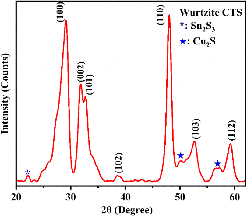 | ||
| Fig. 1 The XRD pattern of deposited CTS TF. | ||
The average crystallite size of deposited CTS TF is determined employing Scherrer's equation,57
 | (1) |
3.2. DRS
The DRS of the CTS TF, shown in Fig. 2(a), reveals an absorption edge around 677 nm, confirming its visible light absorption. Fig. 2(b) illustrates the Tauc plot based on the Kubelka–Munk function to determine the band gap energy. | ||
| Fig. 2 The (a) diffuse reflectance spectrum, and (b) K–M plot of CTS TF. | ||
An estimation of bandgap of deposited CTS TF is carried out by employing following equation,60
| (F(R)·hν)1/n = A(Eg − hν) | (2) |
3.3. AFM
Fig. 3(a and b) depicts the 2D and 3D AFM images of CBD deposited CTS TF. The AFM images suggest uniform distribution along with development of small grains. | ||
| Fig. 3 The (a) 2D and (b) 3D AFM images of CBD deposited CTS TF. | ||
AFM images indicate uniform growth and well-distributed nucleation of the CTS thin film during the CBD process. The film thickness is measured using the gravimetric method.61 The thickness of the deposited films is 1.13 ± 0.01 μm. The Rq and Rrms values of deposited CTS TF are 20.42 ± 5.03 nm and 27.45 ± 7.55 nm respectively which is well matched with previous reports.60,61
4. Experimental and theoretical applications of CTS TF
The following sections explore different optoelectronic applications of the CTS TF, with a comprehensive analysis of the results. The first application focuses on evaluating the photo-response characteristics of the deposited film. For this, the photo-response of a CTS layer is evaluated under a light intensity of 50 mW cm−2 and device parameters such as responsivity, detectivity, sensitivity and photocurrent is determined. In the second application, first ever combined hetero and PEC type CTS-TiO2 solar cell configuration is proposed. TiO2 is selected as the n-type layer due to its widespread use and favorable electronic properties in solar cell.62 To overcome limitations observed during the experimental fabrication of CTS-TiO2 based PEC solar cells, a theoretical model is proposed. In which, heterojunction of CTS layer with Cd based chalcogenides is proposed. In this, alternative n-type layers such as CdS and CdSe are integrated into CTS-CdX configurations and simulated using SCAPS-1D. The simulations further explore the influence of temperature on device performance, with calculations performed for 273, 298, 310, and 373 K. This comprehensive study, combining experimental investigation, device application, and theoretical simulation, highlights the viability of CTS-based materials for future optoelectronic and solar energy applications.4.1. Photo-response properties of deposited CTS TF
The device configuration for evaluating the photo-response properties of deposited CTS TF is shown in Fig. S2.† The photo-response of the CTS thin film is tested by attaching copper wires with silver paste. One end of each wire is connected to the film, and the other end is soldered to a PCB board to complete the measurement setup. To maintain stable electrical contacts during the measurement process the copper wires are fixed to the PCB with glue. The wire-to-film connections, made using silver paste, are heated under an incandescent lamp to improve their conductivity and achieve ohmic contact. These connections are then interfaced with the Keithley-4200 semiconductor characterization system for performance evaluation.Fig. 4(a and b) shows the current–voltage (I–V) characteristics under both dark and white light illumination and the photocurrent versus voltage plot of deposited CTS TF, respectively.
 | ||
| Fig. 4 The (a) I–V characteristics under both dark and white light illumination having intensity of 50 mW cm−2 and (b) photocurrent versus voltage plot of deposited CTS TF. | ||
The linearity observed in the I–V plots under dark and light conditions, shown in Fig. 4(a), confirms the ohmic nature of the contacts on the deposited CTS TF. Under light illumination with intensity of 50 mW cm−2, the current increased due to the photo-generation of charge carriers. As the light is incident on the deposited CTS TF, the concentration of charge carriers increases, leading to an increase in photocurrent depicted in Fig. 4(b). The derivation of photo-response parameters such as photocurrent (Iph), sensitivity (S), responsivity (R), and detectivity (D) in response to applied voltages is done employing the below equations;63
| Iph = Ilight − Idark | (3) |
 | (4) |
 | (5) |
 | (6) |
| Material name | Bias voltage (V) | Iph (μA) | R (mA W−1) | S | D (Jones) | Light source |
|---|---|---|---|---|---|---|
| CTS TF | 1.0 | 28.67 | 5.73 | 114.27 × 10⁻³ | 6.39 × 10¹² | Visible light |
The Table 2 shows the comparative analysis of reported photo-response properties of CTS in different forms.
| No. | CTS | Configuration | D | R | Ref. |
|---|---|---|---|---|---|
| a Poly(3,4 ethylenedioxythiophene):poly(styrenesulfonate). | |||||
| 1 | TF (co-evaporation) | Glass/CTS/Ag | 24 × 106 | 0.14 (A W−1) | 64 |
| 2 | TF (spin coating) | SLG/CTS/Ag | 5.10 × 10¹⁰ | 16.32 (mA W−1) | 65 |
| 3 | Nanostructures (solvothermal) | PET/ITO/PEDOT:PSSa | 8.7 × 10⁹ | 211.5 (mA W−1) | 66 |
| 4 | TF (D.C. sputtering) | SLG/Mo/CTS/CdS, ZnO/GIZnO | 3.9 × 10¹² | 552.3 (A W−1) | 67 |
| 5 | CTS (QD) | SLG/ITO/CTS QD/Ag | 2.79 × 10¹¹ | 1.76 (A W−1) | 66 |
| 6 | CTS (QD) | SLG/ITO/CTS QD/Ag | 2.11 × 10¹⁰ | 7.66 (mA W−1) | 68 |
| 7 | CTS (CBD) | FTO/CTS/Ag | 6.39 × 10¹² | 5.73 (mA W−1) | Present work |
The photo-response parameters of Tables 1 and 2 shows enhanced photocurrent and improved detectivity in present CTS TF, demonstrating excellent photo-response of deposited CTS TF.
4.2. Fabrication of CTS-TiO2 based photo-electrochemical (PEC) type solar cell
In this study, a photoelectrochemical (PEC) solar cell based on a CTS-TiO2 heterojunction is fabricated. A PEC solar cell operates through a semiconductor–electrolyte interface, where photo-generated charge carriers are collected via electrodes.69 CTS has been identified as a suitable candidate for photovoltaic applications owing to its intrinsic p-type conductivity, tunable bandgap within the range of 0.93 to 1.75 eV, high carrier density, and significant optical absorption.70,71 On the other side, TiO2 is used as a potent heterojunction material due to n-type conductivity, a suitable bandgap range of 3.0 to 3.3 eV depending upon various phases, enhanced electron transfer, stability under visible light illumination, and nontoxicity.72,73A two-electrode solar cell configuration is developed in this work. The working electrode consisted of a CTS-TiO2 heterojunction formed on an FTO substrate, with CTS and TiO2 layers deposited using CBD and dip-coating techniques, respectively. The electrode is then annealed at 100 °C for 4 h to facilitate better interfacial contact and structural integrity. The second electrode is a graphite electrode prepared by simply rubbing the pencil on the FTO substrate. The electrolyte solution is prepared by dissolving 0.127 g of iodine (I2) in 10 ml of ethylene glycol, followed by the addition of 0.831 g of potassium iodide (KI), and stirring the mixture for 7 min. The cell fabrication is done by sandwiching prepared iodine electrolyte between the two above-prepared electrodes. The analysis of device parameters is carried out by the Keithley 4200 semiconductor characterization system by measuring I–V measurements. Fig. 5(a and b) shows the picture of the prepared device and the I–V plot of CTS-TiO2 PEC type solar cell, respectively.
 | ||
| Fig. 5 The (a) fabricated device and (b) I–V plot of CTS-TiO2 PEC type solar cell. | ||
The calculation of solar cell parameters is done by employing following equations;74
 | (7) |
 | (8) |
Table 3 shows the obtained solar cell parameters of CTS-TiO2 PEC type solar cell.
| VOC (V) | JSC (mA cm−2) | η (%) | FF (%) |
|---|---|---|---|
| 0.470 | 0.05 | 0.014 | 0.63 |
The Table 3 data states the JSC, VOC, and FF of the prepared CTS-TiO2 cell is low compared to the other reported solar cells based on CTS.75–77 The integration of heterojunction and PEC mechanisms introduces conceptual novelty, their opposing photoresponses create an internal conflict in charge carrier dynamics, leading to poor device performance. Several other factors may be responsible for the present lower values of photovoltaic parameters in this combined solar cell. These limitations of deposition techniques, inefficient charge transfer, small surface area, poor absorber layer quality, leakage currents, unfavorable series/shunt resistance, high recombination rates, and intrinsic material defects.78
4.3. Temperature dependent thickness variations of CTS-CdX (X = S, Se) cell using SCAPS-1D software
Based on the experimental findings, theoretical simulations are conducted to further explore device performance by combining CTS with cadmium-based chalcogenides, replacing TiO2 used in the experimental setup. The experimentally measured thickness (1.13 ± 0.01 μm) and bandgap (1.48 eV) closely match the literature values,75,79,80 thereby supporting the validity of the parameters used in the simulations. Total 32 device simulations based on different thickness and temperature conditions are carried out.In this section, theoretical simulation of a CTS-CdX heterojunction solar cell is carried out using SCAPS-1D simulation software. Very basic device configuration CTS/CdX/FTO is employed for all the simulations. The authors performed thickness variations at different temperatures of 273, 298, 310, and 373 K in order to analyze the effect of temperature on various solar cell parameters such as VOC, JSC, η (%), and FF. Fig. 6 shows the schematic diagram of the proposed device structure.
 | ||
| Fig. 6 Schematic diagram of proposed device structure. | ||
In the thickness variations, the thickness of the p-type CTS layer is varied from 1 to 4 μm. The thicknesses of n-type CdS and CdSe layers are set to their optimum value based on the experimentally reported range of thickness possible by various deposition methods.44,45,81–83 All simulations are undertaken for 1.5 global air mass (AM) sun illuminations (1000 W m−2). The simulated parameters of CTS-CdX device are summarized in Table 4.
| Simulation parameters | p-CTS | n-CdS | n-CdSe | FTO |
|---|---|---|---|---|
| a Variable property. | ||||
| Thickness (μm) | 1 to 4a μm | 2.0 μm | 2.0 μm | 1 μm |
| Bandgap (eV) | 1.0 | 2.40 eV | 1.71 | 3.6 eV |
| Electron affinity (eV) | 4.5 | 4.5 | 4.5 | 4.5 |
| Dielectric permittivity (relative) | 10.00 | 10.00 | 10.00 | 10.00 |
| CB effective density of states (1 cm−3) | 1 × 10¹⁹ | 1 × 10¹⁹ | 1 × 10¹⁹ | 1 × 10¹⁹ |
| VB effective density of states (1 cm−3) | 1 × 10¹⁹ | 1 × 10¹⁹ | 1 × 10¹⁹ | 1 × 10¹⁹ |
| Electron thermal velocity (cm s) | 1 × 10⁷ | 1 × 10⁷ | 1 × 10⁷ | 1 × 10⁷ |
| Hole thermal velocity (cm s) | 1 × 10⁷ | 1 × 10⁷ | 1 × 10⁷ | 1 × 10⁷ |
| Electron mobility (cm2 V s) | 5 × 101 | 5 × 101 | 5 × 101 | 5 × 101 |
| Hole mobility (cm2 V s) | 5 × 101 | 5 × 101 | 5 × 101 | 5 × 101 |
| Shallow uniform donor density (Nd) (1 cm−3) | 1 × 10¹⁹ | 1.1 × 10¹⁷ | 1.1 × 10²⁰ | 2.2 × 10¹⁸ |
| Shallow uniform acceptor density (Na) (1 cm−3) | 1 × 10²⁰ | 1.1 × 10⁸ | 1.1 × 10¹⁰ | 1.1 × 10¹⁸ |
| Radiative recombination coefficient (cm3 s) | 0.00 | 0.00 | 0.00 | 0.00 |
| Contact parameters | ||||
| Front and back contact | ||||
| Flat band condition | ||||
| Surface recombination velocity of hole:1.0 × 105 cm s−1 | ||||
| Surface recombination velocity of electron:1.0 × 107 cm s−1 | ||||
 | ||
| Fig. 7 The J versus V plots of CTS-CdS device at (a) 273, (b) 298, (c) 310, and, (d) 373 K. | ||
The Voc and Jsc variation with thickness for different temperatures of 273, 290, 310 and 398 K are given in below Table 5.
| CTS thickness (μm) | Temperature (K) | |||||||
|---|---|---|---|---|---|---|---|---|
| 273 | 298 | 310 | 373 | |||||
| VOC (V) | JSC (mA cm−2) | VOC (V) | JSC (mA cm−2) | VOC (V) | JSC (mA cm−2) | VOC (V) | JSC (mA cm−2) | |
| 1 | 0.721 | 41.0 | 0.720 | 41.0 | 0.703 | 40.8 | 0.623 | 41.5 |
| 2 | 0.743 | 43.7 | 0.743 | 43.5 | 0.722 | 44.5 | 0.641 | 44.5 |
| 3 | 0.751 | 44.5 | 0.751 | 44.3 | 0.731 | 45.0 | 0.651 | 45.0 |
| 4 | 0.752 | 46.5 | 0.752 | 46.1 | 0.740 | 46.7 | 0.661 | 46.5 |
The data shows the Voc and Jsc decreases with a rise in temperature and increase with the thickness of CTS layer. The deterioration is due to an increase in phonon with temperature in the cell materials. So, low-temperature operation of solar cells is desirable. The cumulative changes in both the values indicate that by providing basic device structure, one can predict the simplest solar cell with significant device characteristics. Fig. 8(a) shows the plots of VOC variation with thickness of CTS for different temperatures. It is clearly observed that as the temperature increases, Voc value decreases. The efficiency versus CTS layer thickness is shown in Fig. 8(b). This also shows the efficiency deteriorating with temperature. Fig. 8(c) shows the efficiency variation with temperature for a CTS thickness of 4 μm. The efficiency continuously decreases with a rise in temperature.
 | ||
| Fig. 8 Comparative plots of (a) VOC versus thickness of CTS layer with variation of temperature, (b) efficiency (η) versus thickness of CTS layer with temperature variation, and (c) efficiency (η) versus temperature (K) for fixed CTS thickness of 4 μm. | ||
As shown in Fig. 8(a–c), the efficiency rises with CTS layer thickness but drops with increasing temperature. The CTS-CdS device demonstrates its best performance at 273 K and for 4 μm thick layer.
 | ||
| Fig. 9 The J versus V plots of CTS-CdSe devices at temperatures of (a) 273, (b) 298, (c) 310 and (d) 373 K. | ||
The Voc and Jsc values for different thicknesses and different temperatures of CTS-CdSe devices are tabulated in Table 6.
| CTS thickness (μm) | Temperature (K) | |||||||
|---|---|---|---|---|---|---|---|---|
| 273 | 298 | 310 | 373 | |||||
| VOC (V) | JSC(mA cm−2) | VOC (V) | JSC (mA cm−2) | VOC (V) | JSC (mA cm−2) | VOC (V) | JSC (mA cm−2) | |
| 1 | 0.753 | 43.2 | 0.721 | 42.1 | 0.700 | 42.6 | 0.621 | 42.4 |
| 2 | 0.771 | 44.1 | 0.742 | 43.9 | 0.721 | 43.9 | 0.644 | 43.7 |
| 3 | 0.782 | 45.6 | 0.750 | 45.4 | 0.740 | 45.2 | 0.660 | 46.3 |
| 4 | 0.780 | 47.0 | 0.753 | 46.7 | 0.744 | 46.7 | 0.664 | 45.3 |
Fig. 10(a and b) shows the comparative plots of VOC and efficiency η versus thickness of the CTS layer at different temperatures. The Fig. 10(c) shows efficiency η versus temperature for fixed CTS thickness of 4 μm.
 | ||
| Fig. 10 Plots of (a) VOC, (b) efficiency (η) as a function of CTS absorber layer thickness at different temperatures and (c) efficiency (η) as a function of tempeature (K) for 4 μm thickness CTS layer. | ||
All the above characteristic plots are of similar nature to that of the CTS-CdS device. The VOC and efficiency values showed an increase with thickness, whereas it illustrates a decreasing trend with temperature. The overall efficiency of the proposed CTS-CdSe device decreases with temperature increase. At 273 K, the proposed CTS-CdSe device delivered a maximum efficiency of 32.08% for a CTS layer thickness of 4 μm. Thus, the CTS layer, having a thickness of 4 μm and an operating temperature of 273 K, is considered an optimum for excellent device parameters. Tables S1 and S2† shows the average and standard deviation calculation of obtained results from CTS-CdS and CTS-CdSe devices respectively.
5. Parametric influences on the experimental and simulated performance of CTS-TiO2 and CTS-CdX devices
Experimentally, the effective suppression of electron–hole recombination is essential for enhancing the stability, efficiency, and durability of the fabricated photovoltaic device.88 In the present study, CTS exhibits a high carrier concentration in the range of ∼1018–1019 cm−3.89 Such a high density of charge carriers increases the probability of electron–hole recombination within the material. In addition, defects in the crystal lattice can act as trap states, promoting charge carrier recombination and reducing device efficiency.90 Poor adhesion of the CTS thin film to the substrate can hinder device efficiency; therefore, adopting an alternative deposition approach and optimizing related parameters may yield improved film quality and performance.31 In CBD, both deposition time and temperature are vital parameters that dictate CTS film uniformity and thickness. The deposition temperature and time significantly affects the structural integrity, while the bath temperature governs the crystallinity of the resulting thin films.91,92 Various other physical deposition techniques such as sputtering, thermal evaporation, and spray pyrolysis offers advantages over CBD by ensuring better film-substrate adhesion and more consistent thickness, which are key to achieving reliable and efficient device operation over longer time span.32,93,94 To enhance photovoltaic performance, CTS can be paired with diverse n-type materials such as ZnS, CdS, CdSe, ZnO, or perovskite systems based on CH3NH3(Sn,Pb)(Br,I)3, which have shown promising efficiencies nearing 20% in reported studies.53,95–97While desinging the device in software, device parameters such as back and front contacts, metal work functions, HOMO and LUMO levels, donor and acceptor density of the materials, temperature, bandgap of the material, thickness of the absorber layer, interface properties of layers, defect densities, charge carrier lifetime, etc., are considered key parameters that deeply affect the VOC, JSC, and η.98 In the present case of the CTS-CdX device, as the thickness of the CTS absorber layer is increased from 1 to 4 μm, the photon absorption increases, leading to enhanced current density, thus augmenting efficiency and fill factor.98 Elevation of recombination rate in any layer depends upon the optimum thickness of that layer.38 Determination of the optimum CTS layer thickness depends upon several factors, such as bandgap range (0.96–1.75 eV),99 experimental deposition conditions (pH, temperature, adhesion),100 high absorption coefficient ∼105 cm−1,38,101 etc. The device response of the CTS-CdX configuration is found to decrease as the temperature increases from 273 to 373 K. As the temperature increases, the phonon contribution increases, leading to hindrance to carrier flow, thus decreasing the voltage and output power of the CTS-CdX device.98 Parameters such as ohmic loss, which consists of series and shunt resistances, recombination loss, reverse saturation current, reduction loss, etc., are also responsible for the drastic changes in VOC, JSC, and efficiency of the device. Singh et al.102 demonstrated that the reverse saturation current density (J0) which arises due to minority charge carriers which affects the overall performance of the device. The equation of J0 is given as follow;102,103
 | (9) |
In both theoretical and experimental fabrication of CTS-based heterojunction solar cells, interfacial properties play a pivotal role. Imperfections or energy misalignments at the interfaces where CTS is sandwiched can create recombination centers, thereby lowering the VOC and JSC values of the device.107 At the interface, the presence of defects acts as the trapping sites, which trap the charge carriers and prevent them from reaching the electrode. Rapid recombination at trap sites limits charge carrier collection, resulting in lower current and poor cell efficiency.108,109
Table 7 shows the comparative analysis of solar cell parameters reported for various configurations using SCAPS-1D.
| No. | Device configuration | Eg (CTS) (eV) | Thickness (CTS) (μm) | Solar cell parameters | Ref. | |||
|---|---|---|---|---|---|---|---|---|
| JSC mA cm−2 | VOC (V) | η (%) | FF (%) | |||||
| 1 | iZnO/CdS/p-CTS | 1.25 | 4.0 | 35.0 | 0.712 | 20.3 | — | 110 |
| 2 | p-CTS/n-CdS/i-ZnO/n-ZnO:Al | 0.91 | 2.5 | 48.6 | 0.580 | 22.3 | 78.09 | 111 |
| 3 | ITO/ZnSe/CTS/Cu2O/Au | 1.21 | 0.4 | 37.2 | 0.940 | 30.0 | 86.87 | 38 |
| 4 | n-ZnSe/p-CTS | — | — | 32.3 | 0.602 | 17.6 | 80.58 | 39 |
| 5 | Al/n-ZnO:Al/i-ZnO/n-CdS/p-CTS/Mo/SLG | 0.96 | 1 to 4 | >24.0 | 0.703 | 12.0 | 0.3 to 0.8 | 112 |
| 6 | SLG/Mo/CTS/ZnS/ITO/Al | — | — | 24.6 | 1.091 | 20.3 | 75.23 | 21 |
| 7 | FTO/CdS/CTS | 1.0 | 4.0 | ∼46.5 | ∼0.720 to 0.753 | 31.8 | 86.88 | Present work |
| 8 | FTO/CdSe/CTS | 1.0 | 4.0 | ∼47.1 | ∼0.750 to 0.781 | 32.0 | 86.90 | Present work |
The analysis of the parameters of Table 7 clearly shows that the present configuration studied by authors has potential for device improvements experimentally by involving the CTS material.
6. Conclusion
The CTS thin film, synthesized using the CBD technique, exhibited a wurtzite crystalline phase as identified by XRD. Surface morphology assessments via AFM confirmed a uniform and well-distributed film on the FTO substrate. Optical characterization through DRS and the Kubelka–Munk approach indicated visible-range absorption and a direct bandgap of 1.48 eV. These findings qualified the film for use in multiple optoelectronic applications, such as light-response measurements, PEC solar cell fabrication, and theoretical simulations with SCAPS-1D. The deposited CTS thin film was analyzed for its photo-response behaviour under both dark and illuminated conditions. An increase in photocurrent was observed as the bias voltage was raised from 1 V to 2 V. At 1 V bias, the CTS TF demonstrated a responsivity of 5.73 mA W−1, a sensitivity of 114.27 × 10⁻³, and a detectivity of 6.39 × 10¹² Jones, indicating its promising potential for optoelectronic applications. In another application, the PEC CTS-TiO2 solar cell exhibited a current density of 0.05 mA cm−2, an open-circuit voltage of 0.470 V, an efficiency of 0.014%, and a fill factor of 0.63. Although the obtained efficiency is found to be low, this hybrid operation opens up new possibilities for dual-mode solar cell configurations, particularly in next-generation energy conversion systems. To overcome the relatively low efficiency observed in experimental PEC solar cells, theoretical simulations are conducted using SCAPS-1D. Here, TiO2 was replaced with CdX (X = S, Se) as the n-type layer to examine the impact on device performance. The proposed device CTS-CdX (X = S, Se) works excellently at 273 K and moderately at 310 K. Furthermore, an increase in temperature is observed to negatively impact the overall device performance. To achieve higher efficiencies in practical applications, it is essential to focus on fine-tuning intrinsic parameters such as charge carrier dynamics, interface recombination, and band alignment. These factors directly influence the voltage output and energy conversion capability of the device and represent vital targets for future research. This can be achieved by controlling operating temperature, hole–electron mobility, and thermal velocity, sandwiching various perovskite layers, and making heterojunctions of compounds such as ZnX (X = S, Se, and Te), ZnO, PbO, PbX (X = S, Se, and Te), etc. Given their promising experimental and theoretical performance, CTS-based devices emerge as strong candidates for replacing traditional silicon and germanium counterparts in next-generation solar technologies.Data availability
The data included in this manuscript is completely carried out by the authors.Conflicts of interest
There is no conflict of interest to declare for this work.Acknowledgements
The authors of this manuscript are sincerely thankful to Prof. M. Burgelman and his team at University of Ghent, Belgium for providing the SCAPS-1D simulation software. The authors are also thankful to Dr Jayesh Gandhi for XRD, Sophisticated Instrumentation Centre for Applied Research and Testing (SICART) for DRS and Dr SaurabhS.Soni, P.G. Department of Chemistry, Sardar Patel University for AFM.References
- M. Ravindiran and C. Praveenkumar, Renewable Sustainable Energy Rev., 2018, 94, 317–329 CrossRef CAS
.
- G. K. Weldegebrieal, Inorg. Chem. Commun., 2020, 120, 108140 CrossRef CAS
- L. Wang, W. Ma, L. Xu, W. Chen, Y. Zhu, C. Xu and N. A. Kotov, Mater. Sci. Eng., R, 2010, 70, 265–274 CrossRef
- P. P. Li, X. P. Liu, C. J. Mao, B. K. Jin and J. J. Zhu, Anal. Chim. Acta, 2019, 1048, 42–49 CrossRef CAS PubMed
- G. Konstantatos, J. Clifford, L. Levina and E. H. Sargent, Nat. Photonics, 2007, 1, 531–534 CrossRef CAS
- K. Ramakrishnan, B. Ajitha and Y. A. K. Reddy, Sens. Actuators, A, 2023, 349, 114051 CrossRef CAS
- T. D. Lee and A. U. Ebong, Renewable Sustainable Energy Rev., 2017, 70, 1286–1297 CrossRef CAS
- M. A. Green, in Seventh EC Photovoltaic Solar Energy Conference, Springer, 1987, pp. 681–687 Search PubMed
- T. Matsui, H. Sai, A. Bidiville, H.-J. Hsu and K. Matsubara, Sol. Energy, 2018, 170, 486–498 CrossRef CAS
- V. Kumar, R. Prasad, N. B. Chaure and U. P. Singh, in Recent Advances in Thin Film Photovoltaics, Springer, 2022, pp. 5–39 Search PubMed
- R. Garza-Hernández, H. J. Edwards, J. T. Gibbon, M. R. Alfaro-Cruz, V. R. Dhanak and F. S. Aguirre-Tostado, J. Alloys Compd., 2021, 881, 160552 CrossRef
- H. Ming, G. Zhu, C. Zhu, X. Qin, T. Chen, J. Zhang, D. Li, H. Xin and B. Jabar, ACS Nano, 2021, 15, 10532–10541 CrossRef CAS PubMed
- Y.-H. A. Wang, N. Bao and A. Gupta, Solid State Sci., 2010, 12, 387–390 CrossRef CAS
- J. M. Delgado, G. D. De Delgado, M. Quintero and J. C. Woolley, Mater. Res. Bull., 1992, 27, 367–373 CrossRef CAS
- B. Yang, L. Wang, J. Han, Y. Zhou, H. Song, S. Chen, J. Zhong, L. Lv, D. Niu and J. Tang, Chem. Mater., 2014, 26, 3135–3143 CrossRef CAS
- D. Xue, B. Yang, Z. Yuan, G. Wang, X. Liu, Y. Zhou, L. Hu, D. Pan, S. Chen and J. Tang, Adv. Energy Mater., 2015, 5, 1501203 CrossRef
- Y. Shen, C. Li, R. Huang, R. Tian, Y. Ye, L. Pan, K. Koumoto, R. Zhang, C. Wan and Y. Wang, Sci. Rep., 2016, 6, 32501 CrossRef CAS PubMed
- A. Rabhi, M. Kanzari and B. Rezig, Thin Solid Films, 2009, 517, 2477–2480 CrossRef CAS
- J. Navrátil, P. Levinský, J. Hejtmanek, M. Pashchenko, K. Knížek, L. Kubíčková, T. Kmječ and C. Drašar, J. Phys. Chem. C, 2020, 124, 20773–20783 CrossRef
- R. Chierchia, F. Pigna, M. Valentini, C. Malerba, E. Salza, P. Mangiapane, T. Polichetti and A. Mittiga, Phys. Status Solidi, 2016, 13, 35–39 CAS
- Y. Nouri, B. Hartiti, A. Batan, A. Ziti, H. Labrim, A. Ouannou, A. Laazizi, S. Fadili, M. Tahri and P. Thévenin, Opt. Mater., 2023, 137, 113602 CrossRef CAS
- L. L. Baranowski, P. Zawadzki, S. Christensen, D. Nordlund, S. Lany, A. C. Tamboli, L. Gedvilas, D. S. Ginley, W. Tumas and E. S. Toberer, Chem. Mater., 2014, 26, 4951–4959 CrossRef CAS
- A. Shigemi, T. Maeda and T. Wada, Phys. Status Solidi, 2015, 252, 1230–1234 CrossRef CAS
- C. Li, H. Song, Y. Cheng, R. Qi, R. Huang, C. Cui, Y. Wang, Y. Zhang and L. Miao, ACS Appl. Energy Mater., 2021, 4, 8728–8733 CrossRef CAS
- S. Nakamura, H. Funabiki and S. Shiga, Phys. Status Solidi C, 2017, 14, 1600172 CrossRef
- K. Lohani, H. Nautiyal, N. Ataollahi, C. Fanciulli, I. Sergueev, M. Etter and P. Scardi, J. Phys. Chem. C, 2020, 125, 178–188 CrossRef
- J. B. Raval, S. H. Chaki, B. S. Shah and M. P. Deshpande, Mater. Today: Proc., 2023, 73(Part 4), 562–566 CAS
- S. Petrosyan, A. Musayelyan, E. Zaretskaya, V. Gremenok, K. Buskis and A. Stanchik, Chalcogenide Lett., 2023, 20, 811–820 CrossRef CAS
- S. Rabaoui, H. Dahman, S. Dekhil, K. Omri, A. Alyamani and L. El Mir, J. Mater. Sci.:Mater. Electron., 2015, 26, 8588–8594 CrossRef CAS
- Y. Igarashi, T. Tomono, K. Tanaka and K. Moriya, Jpn. J. Appl. Phys., 2022, 61, SB1002 CrossRef CAS
- J. Raval, B. Shah, D. Kumar, S. H. Chaki and M. P. Deshpande, Chem. Eng. Sci., 2024, 119728 CrossRef CAS
- A. Kanai, K. Toyonaga, K. Chino, H. Katagiri and H. Araki, Jpn. J. Appl. Phys., 2015, 54, 08KC06 CrossRef
- J. Li, C. Xue, Y. Wang, G. Jiang, W. Liu and C. Zhu, Sol. Energy Mater. Sol. Cells, 2016, 144, 281–288 CrossRef CAS
- M. Nakashima, J. Fujimoto, T. Yamaguchi and M. Izaki, Appl. Phys. Express, 2015, 8, 42303 CrossRef
- A. Kanai and M. Sugiyama, Sol. Energy Mater. Sol. Cells, 2021, 231, 111315 CrossRef CAS
- S. S. Bal, A. Basak and U. P. Singh, Opt. Mater., 2022, 127, 112282 CrossRef CAS
- D. Roy, R. Garain, A. Basak, S. Behera, R. Patel and U. P. Singh, in Recent Advances in Power Systems: Select Proceedings of EPREC 2022, Springer, 2023, pp. 63–75 Search PubMed
- A. Siddique, M. Nurul Islam, H. Karmaker, A. K. M. Asif Iqbal, A. Al Mazed Khan, M. Aminul Islam and B. Kumar Das, Results Opt., 2024, 16, 100713 CrossRef
- M. J. Nayeen, B. K. Mondal, S. R. Basu and J. Hossain, Sol. Energy, 2023, 265, 112076 CrossRef CAS
- S. E. Lachhab, A. Bliya, K. Nabaoui, E. Al Ibrahmi and L. Dlimi, Aust. J. Electr. Electron. Eng., 2024, 21, 29–35 CrossRef
- S. M. Yadav and A. Pandey, Mater. Res. Innov., 2023, 27, 503–510 CrossRef CAS
- M. R. Butaev, V. I. Kozlovsky and Y. K. Skasyrsky, Opt. Laser Technol., 2023, 158, 108890 CrossRef CAS
- S. I. S. Mashuri, M. F. Kasim, N. H. M. Kaus, Y. H. Tan, A. Islam, U. Rashid, N. Asikin-Mijan, J. Andas, Y. H. Taufiq-Yap and M. K. Yaakob, Renewable Sustainable Energy Rev., 2023, 184, 113602 CrossRef
- M. Kamalian, E. Hasani, L. B. Habashi and M. G. Arashti, Phys. Rev. B: Condens. Matter Mater. Phys., 2024, 674, 415524 CrossRef CAS
- A. A. Faremi, P. A. Olubambi, A. O. Salau and A. A. Ibiyemi, Results Eng., 2023, 18, 101039 CrossRef CAS
- E. Ö. Alagöz, H. Jahangiri and S. Kaya, Mater. Adv., 2024, 5, 1513–1522 RSC
- M. D. A. H. Pappu, A. Kuddus, B. K. Mondal, A. T. Abir and J. Hossain, Opt. Continuum, 2023, 2, 942–955 CrossRef CAS
- R. V Ingle, S. F. Shaikh, J. Kaur, M. Ubaidullah, B. Pandit and H. M. Pathan, Mater. Sci. Eng., B, 2023, 294, 116487 CrossRef
- J. A. Melchor-Robles, K. E. Nieto-Zepeda, N. E. Vázquez-Barragán, M. Arreguín-Campos, K. Rodríguez-Rosales, J. Cruz-Gómez, A. Guillén-Cervantes, J. Santos-Cruz, M. D. L. L. Olvera and G. Contreras-Puente, Coatings, 2024, 14, 452 CrossRef CAS
- P. M. Perillo and D. F. Rodriguez, Phys. Rev. B: Condens. Matter Mater. Phys., 2024, 680, 415828 CrossRef CAS
- D. Kumar, C. Lal, D. Veer, D. Singh, P. Kumar and R. S. Katiyar, Mater. Lett.:X, 2023, 18, 100204 CAS
- R. I. Jasim, E. H. Hadi, S. S. Chiad, N. F. Habubi, M. Jadan and J. S. Addasi, J. Ovonic Res., 2023, 19, 187 CrossRef CAS
- W. Ho and C. Y. Jimmy, J. Mol. Catal. A: Chem., 2006, 247, 268–274 CrossRef CAS
- R. S. Singh, S. Bhushan, A. K. Singh and S. R. Deo, Dig. J. Nanomater. Biostructures, 2011, 6, 403 Search PubMed
- D. Parajuli, K. C. Devendra, K. B. Khattri, D. R. Adhikari, R. A. Gaib and D. K. Shah, Sci. Rep., 2023, 13, 12193 CrossRef CAS PubMed
- M. Belaqziz, K. Medjnoun, K. Djessas, H. Chehouani and S. E. Grillo, Mater. Res. Bull., 2018, 99, 182–188 CrossRef CAS
- P. Scherrer, Nach Ges Wiss Gottingen, 1918, 2, 8–100 Search PubMed
- J. Il Langford and A. J. C. Wilson, Appl. Crystallogr., 1978, 11, 102–113 CrossRef
- V. Uvarov and I. Popov, Mater. Charact., 2007, 58, 883–891 CrossRef CAS
- A. R. Machale, H. D. Shelke, S. A. Phaltane and L. D. Kadam, Chem. Phys. Lett., 2022, 808, 140097 CrossRef CAS
- S. H. Chaki, M. P. Deshpande and J. P. Tailor, Thin Solid Films, 2014, 550, 291–297 CrossRef CAS
- S. M. H. Al-Jawad, M. Rasheed and Z. Y. Abbas, J. Opt., 2024, 1–22 Search PubMed
- S. R. Patel, S. H. Chaki, S. V Bhatt, M. P. Deshpande, S. S. Soni and S. N. Bariya, Thin Solid Films, 2024, 791, 140242 CrossRef CAS
- T. S. Reddy and M. C. S. Kumar, J. Ovonic Res., 2019, 15(6), 365–376 CAS
- S. Dias and S. B. Krupanidhi, AIP Adv., 2016, 6, 25217 CrossRef
- S. Dias and S. B. Krupanidhi, Mater. Res. Express, 2016, 3, 105006 CrossRef
- S. Dias, S. Chirakkara, N. Patel and S. B. Krupanidhi, J. Mater. Sci.:Mater. Electron., 2018, 29, 2131–2139 CrossRef CAS
- S. Dias, K. Kumawat, S. Biswas and S. B. Krupanidhi, Inorg. Chem., 2017, 56, 2198–2203 CrossRef CAS PubMed
- G. Hodes, J. Phys. Chem. Lett., 2012, 3, 1208–1213 CrossRef CAS PubMed
- A. C. Lokhande, A. Shelke, P. T. Babar, J. Kim, D. J. Lee, I.-C. Kim, C. D. Lokhande and J. H. Kim, RSC Adv., 2017, 7, 33737–33744 RSC
- T. A. Kuku and O. A. Fakolujo, Sol. Energy Mater., 1987, 16, 199–204 CrossRef CAS
- Y. Nosaka and A. Y. Nosaka, J. Phys. Chem. Lett., 2016, 7, 431–434 CrossRef CAS PubMed
- A. Panepinto, A. Krumpmann, D. Cornil, J. Cornil and R. Snyders, Appl. Surf. Sci., 2021, 563, 150274 CrossRef CAS
- M. Abdelfatah, W. Ismail, N. M. El-Shafai and A. El-Shaer, Mater. Technol., 2021, 36, 712–720 CrossRef CAS
- S. Thiruvenkadam, P. Sakthi, S. Prabhakaran, S. Chakravarty, V. Ganesan and A. L. Rajesh, Phys. Rev. B: Condens. Matter Mater. Phys., 2018, 538, 8–12 CrossRef CAS
- M. Nakashima, T. Yamaguchi, H. Itani, J. Sasano and M. Izaki, Phys. Status Solidi, 2015, 12, 761–764 CAS
- Y. Wang, J. Li, C. Xue, Y. Zhang, G. Jiang, W. Liu and C. Zhu, J. Mater. Sci., 2017, 52, 6225–6234 CrossRef CAS
- S. Sikiru, T. L. Oladosu, T. I. Amosa, S. Y. Kolawole and H. Soleimani, J. Energy Storage, 2022, 53, 105200 CrossRef
- H. Dahman, S. Rabaoui, A. Alyamani and L. El Mir, Vacuum, 2014, 101, 208–211 CrossRef CAS
- M. R. Pallavolu, R. R. Nallapureddy, S. W. Joo and C. Park, Opt. Mater., 2021, 111, 110668 CrossRef CAS
- A. El-Shaer, S. Ezzat, M. A. Habib, O. K. Alduaij, T. M. Meaz and S. A. El-Attar, Crystals, 2023, 13(5), 788 CrossRef CAS
- L. N. Ibrahimova, N. M. Abdullayev, S. R. Azimova and Y. I. Aliyev, East Eur. J. Phys., 2024, 293–296 CrossRef
- X. Liu, A. Abbas, M. Togay, V. Kornienko, R. Greenhalgh, K. Curson, J. Bowers, K. Barth, M. Walls and E. Bastola, Sol. Energy Mater. Sol. Cells, 2024, 267, 112717 CrossRef CAS
- V. Gadore, S. R. Mishra and M. Ahmaruzzaman, Sci. Rep., 2023, 13, 7708 CrossRef CAS PubMed
- W. Ismail, G. Ibrahim, M. A. Habib, O. K. Alduaij, M. Abdelfatah and A. El-Shaer, Nanomaterials, 2023, 13, 1764 CrossRef CAS PubMed
- Z. Ju, X. Qi, S. Schaefer, M. R. McCartney, D. J. Smith, A. V. G. Chizmeshya, T. McCarthy, A. McMinn, S. Grover and Y.-H. Zhang, IEEE J. Photovoltaics., 2024, 14(5), 752–757 Search PubMed
- M. H. Huseynaliyev and L. N. Ibrahimova, Optical Properties Of Cdse Thin Films Produced By The Cbd Method From Four-Component And Three-Component Solutions.
- E. Singh and H. S. Nalwa, RSC Adv., 2015, 5, 73575–73600 RSC
- B. Patel, R. K. Pati, I. Mukhopadhyay and A. Ray, J. Anal. Appl. Pyrolysis, 2018, 136, 35–43 CrossRef CAS
- O. Z. Sharaf and M. F. Orhan, Renewable Sustainable Energy Rev., 2015, 50, 1500–1565 CrossRef
- B. Y. Taher and A. S. Ahmed, Chalcogenide Lett., 2021, 18, 717–724 CrossRef CAS
- M. F. A. Alias, B. Y. Taher, I. S. Naji, S. Iqbal, A. Kayani, M. F. Mabrook and A. A. J. Al-Douri, Chalcogenide Lett., 2019, 16(12), 577–586 CAS
- M. He, A. C. Lokhande, I. Y. Kim, U. V. Ghorpade, M. P. Suryawanshi and J. H. Kim, J. Alloys Compd., 2017, 701, 901–908 CrossRef CAS
- M. H. Sayed, E. V. C. Robert, P. J. Dale and L. Gütay, Thin Solid Films, 2019, 669, 436–439 CrossRef CAS
- M. W. Dlamini, M. S. G. Hamed, X. G. Mbuyise and G. T. Mola, J. Mater. Sci.:Mater. Electron., 2020, 31, 9415–9422 CrossRef CAS
- N. Romeo, A. Bosio, V. Canevari and A. Podestà, Sol. Energy, 2004, 77, 795–801 CrossRef CAS
- H.-J. Du, W.-C. Wang and J.-Z. Zhu, Chin. Phys. B, 2016, 25, 108802 CrossRef
- R. Hosen, S. Sikder, M. S. Uddin, M. M. Haque, H. Mamur, M. R. A. Bhuiyan and J. Alloy, Metall. Syst., 2023, 4, 100041 Search PubMed
- S. B. Jathar, S. R. Rondiya, Y. A. Jadhav, D. S. Nilegave, R. W. Cross, S. V Barma, M. P. Nasane, S. A. Gaware, B. R. Bade, S. R. Jadkar, A. M. Funde and N. Y. Dzade, Chem. Mater., 2021, 33, 1983–1993 CrossRef CAS PubMed
- H. D. Shelke, A. C. Lokhande, J. H. Kim and C. D. Lokhande, J. Colloid Interface Sci., 2017, 506, 144–153 CrossRef CAS PubMed
- S. P. Meenakshisundaram and M. B. Sridharan, J. Alloys Compd., 2024, 981, 173734 CrossRef CAS
- P. Singh and N. M. Ravindra, Sol. Energy Mater. Sol. Cells, 2012, 101, 36–45 CrossRef CAS
- D. Das, P. Kalita and O. Roy, Renewable Sustainable Energy Rev., 2018, 84, 111–130 CrossRef
- G. Bakan, N. Khan, H. Silva and A. Gokirmak, Sci. Rep., 2013, 3, 2724 CrossRef PubMed
- R. K. Ahrenkiel, in Semiconductors and Semimetals, Elsevier, 1993, vol. 39, pp. 39–150 Search PubMed
- P. Löper, D. Pysch, A. Richter, M. Hermle, S. Janz, M. Zacharias and S. W. Glunz, Energy Procedia, 2012, 27, 135–142 CrossRef
- R. N. Pandey, K. S. C. Babu and O. N. Srivastava, Prog. Surf. Sci., 1996, 52, 125–192 CrossRef CAS
- F. A. Lindholm, J. J. Liou, A. Neugroschel and T. W. Jung, IEEE Trans. Electron Devices, 1987, 34, 277–285 Search PubMed
- R. H. Sardar, A. Bera, S. Chattopadhyay, S. I. Ali, S. Pramanik and A. C. Mandal, Opt. Mater., 2024, 155, 115818 CrossRef CAS
- I. S. Amiri, H. Ahmad, M. M. Ariannejad, M. F. Ismail, K. Thambiratnam, M. Yasin and N. M. A. Nik Abdul-Aziz, Surf. Rev. Lett., 2016, 24, 1750073 CrossRef
- A. S. Mathur, S. Upadhyay, P. P. Singh, B. Sharma, P. Arora, V. K. Rajput, P. Kumar, D. Singh and B. P. Singh, Opt. Mater., 2021, 119, 111314 CrossRef CAS
- M. Ali, M. A. Abedin, M. S. Hossain and E. S. Hossain, Chalcogenide Lett., 2020, 17, 85–98 CrossRef CAS
Footnote |
| † Electronic supplementary information (ESI) available. See DOI: https://doi.org/10.1039/d5ra03157e |
| This journal is © The Royal Society of Chemistry 2025 |