DOI:
10.1039/D5RA02866C
(Paper)
RSC Adv., 2025,
15, 17365-17376
Structural, electrical, and optical properties of NiO films for surface-enhanced Raman spectroscopy applications
Received
24th April 2025
, Accepted 19th May 2025
First published on 23rd May 2025
Abstract
This study investigates the structural, electrical, and optical properties of NiO thin films deposited by DC sputtering in an Ar/O2 atmosphere with varying oxygen concentrations. As the O2 content increases, energy-dispersive X-ray (EDX) analysis reveals a higher concentration of Ni vacancies and Ni3+ ions, resulting in lower resistivity and a slight reduction in crystal quality. Among the samples, the film grown at 50% oxygen (NiO-50) exhibits the best combination of properties for Surface-Enhanced Raman Spectroscopy (SERS), including balanced crystallinity, surface roughness, and high hole concentration. Current–voltage (I–V) measurements and Raman spectra using Rhodamine 6G (10−9 M) confirm that the SERS enhancement is driven by an electron transition mechanism. The calculated enhancement factor of 9.6 × 10⁸ for the NiO/Si substrate surpasses previously reported values. These results position NiO-50 as a promising SERS-active material and provide insights into tuning NiO film properties for enhanced sensing applications.
1. Introduction
Nickel oxide (NiO) is a p-type semiconductor with a wide bandgap of 3.5–4.0 eV, high electrical resistivity, and excellent transparency in the visible region.1–5 These characteristics make NiO a promising candidate for diverse applications such as transparent conducting oxides (TCOs) in solar cells,3,6,7 light-emitting diodes (LEDs),8–10 photodetectors,11–13 thin-film transistors,14 electrochromic windows,15–22 gas sensors,23,24 and water splitting devices.25,26 Structurally, NiO typically exhibits a rock-salt (FCC) configuration, though it may adopt cubic or monoclinic phases depending on the synthesis conditions.
NiO thin films can be prepared via various deposition techniques. Chemical methods such as sol–gel,7,13,21 chemical bath deposition (CBD),17,20 and hydrothermal synthesis26 are cost-effective and suitable for large-area coating but often suffer from poor control over film uniformity, crystallinity, and stoichiometry. Atomic layer deposition (ALD)27 offers superior thickness control and conformality but is limited by high cost and low deposition rates. Among physical vapor deposition (PVD) methods, radio frequency (RF) magnetron sputtering28–34 enables good stoichiometric control and uniformity, but the systems are complex and expensive. High-power impulse magnetron sputtering (HiPIMS)4,35 improves film density and crystallinity due to high ionization but suffers from low deposition rates and higher operational complexity. In contrast, direct current (DC) magnetron sputtering1,4,15 presents a practical balance—offering uniform, reproducible NiO films with tunable properties, low cost, and scalability. Therefore, DC sputtering was selected in this study.
Surface-enhanced Raman spectroscopy (SERS) is a powerful technique that amplifies Raman scattering signals, enabling the detection of trace molecules with high sensitivity. Typically, SERS relies on two enhancement mechanisms: electromagnetic (EM) enhancement, originating from localized surface plasmon resonance (LSPR) in noble metal nanostructures (e.g., Ag, Au), and chemical (CM) enhancement, which involves charge transfer between the substrate and the analyte. While most studies have focused on plasmonic metal-based substrates, increasing interest has emerged in semiconductor-based SERS systems due to their chemical tunability, stability, and potential for cost-effective fabrication.
NiO has recently been explored as a component in hybrid SERS substrates, typically in combination with Ag nanoparticles to leverage LSPR-based enhancement. Examples include NiO/Ag nanowells,36 nanowires,37 nanoflowers,38 and nanopetals,39 all demonstrating notable SERS activity. However, in these cases, the enhancement is primarily attributed to the plasmonic effect of Ag. In contrast, this study focuses on pure NiO thin films without any plasmonic metal inclusion. This allows the investigation of an alternative, non-plasmonic enhancement mechanism—photoinduced charge transfer from NiO to the lowest unoccupied molecular orbital (LUMO) of adsorbed probe molecules such as Rhodamine 6G under laser excitation. By combining SERS spectral data and current–voltage (I–V) measurements, we provide evidence supporting this chemical enhancement mechanism. To the best of our knowledge, this is the first report on SERS enhancement using standalone NiO thin films, offering new insights into semiconductor-mediated Raman amplification.
Previous reports have demonstrated that NiO films fabricated via DC1,4,15 or RF28–34 sputtering in Ar/O2 gas mixtures exhibit varying hole concentrations, strongly influenced by Ni vacancies and Ni3+ content, which are in turn affected by O2 flow rate. However, many of these methods yield films with inferior crystal quality, including poor crystal quality, irregular or small grain sizes, and phase non-uniformity. For instance, low sputtering power or insufficient substrate temperature during RF sputtering often leads to amorphous or poorly crystalline films,15,28–30,33 while broad XRD peaks indicate limited grain growth.28,30,33 Improvement in crystallinity typically requires higher substrate or annealing temperatures1,29,31 or elevated sputtering power in HiPIMS systems.35
In this work, we deposited NiO films using DC magnetron sputtering at room temperature, systematically varying the O2 gas ratio to study its influence on film crystallinity and hole concentration. We then evaluated the SERS performance of these films to understand how crystal quality and charge carrier density affect the photoinduced charge transfer mechanism. The findings provide a deeper understanding of semiconductor-based SERS systems and offer a viable route for fabricating non-plasmonic SERS substrates.
2. Experiment
2.1 Synthesis of NiO films
NiO thin films were deposited on glass substrates (Marrienfeld, Germany) and n-type CZ Si (100) wafers, single-side polished, with a resistivity of 1–10 Ω cm and (100) orientation. The surface of the glass substrate was initially cleaned in sequence with NaOH, CH3COCH3, and distilled water using an ultrasonic bath. The silicon substrates were subjected to ultrasonic cleaning with a solution of 5% HF acid, C2HCl3, CH3CH(OH)CH3, CH3COCH3, and distilled water. The substrates were subsequently positioned in a vacuum system (Leybold Univex 450, Germany) which was withdrew to an atmosphere pressure of 10−6 torr before sputtering. A mixture of oxygen and argon gas (99.9999% purity) was injected into the vacuum chamber via two flowmeter (resolution 0.1 SCCM) at a total flow rate of 35 sccm, in accordance with the desired ratio. The working pressure was maintained at 2 × 10⁻³ torr, and direct current magnetron sputtering was utilized to deposit the films using a nickel target with 99.99% purity. The DC source power and target-substrate distance was set at 70 W and 7 cm, respectively, while the O2 concentration in the sputtering mixed gas was adjusted at varying percentages x% (where x ranges from 10 to 60 in increments of 10, with x representing the ratio of O2 to the sputtering mixed gas). The names of NiO films are assigned based on the various manufactured conditions as indicated in Table 1.
Table 1 The NiO samples deposited on glass and Si substrates at x% (x = 10, 20, 30, 40, 50, and 60) O2 gas in a mixture of O2 and Ar gas
| Sample |
Substrate |
% Ar gas |
% O2 gas |
Description |
| NiO-10 |
Glass and Si |
90 |
10 |
NiO-x samples investigated in analyses such as EDX, XRD, FESEM, AFM, UV-vis |
| NiO-20 |
Glass and Si |
80 |
20 |
| NiO-30 |
Glass and Si |
70 |
30 |
| NiO-40 |
Glass and Si |
60 |
40 |
| NiO-50 |
Glass and Si |
50 |
50 |
| NiO-60 |
Glass and Si |
40 |
60 |
| R6G/NiO-x |
Glass |
100 − x |
x |
R6G dropped on NiO-x in Raman analysis at 10−5 M concentration |
| R6G/NiO-50/glass-10−5 M |
Glass |
50 |
50 |
R6G dropped on NiO-x in Raman analysis at 10−5 M |
| R6G/NiO-50/Si-y M |
Si |
50 |
50 |
R6G dropped on NiO-50/Si in Raman analysis at y M |
| R6G/NiO-50/Si-10−9 M-10−4 V |
Si |
50 |
50 |
R6G dropped on NiO-50/Si in Raman analysis at 10−9 M with 10−4 V bias |
| R6G/NiO-50/Si-10−9 M-1.5 V |
Si |
50 |
50 |
R6G dropped on NiO-50/Si in Raman analysis at 10−9 M with 1.5 V bias |
2.2 Material characterization
The surface, cross-sectional morphology, and elemental content of NiO films were investigated using a JEOL JSM – IT800SHL Field Emission Electron Microscope (FE-SEM). The films' smoothness was observed using atomic force microscopy (AFM) on Agilent 5500 system. The crystal structural quality of the films was tested using X-wavelength diffraction (XRD) using the Rigaku Ultima IV system utilizing a Cu–K radiation source. The electrical properties were conducted at 28 °C using the HL5500PC system. The absorption spectra of NiO were obtained from 200 to 1100 nm using the Agilent Cary 300. The photocurrent response of NiO/Si was evaluated by investigating the current plot versus voltage under illuminated and non-illuminated conditions, employing a Keithley system (model 2450) and a 532 nm green light source with an illuminated energy of 5 mW cm−2.
2.3 SERS characterizations
To assess the SERS signal amplification of NiO substrates, Rhodamine 6G (R6G) was solubilized in distilled water and employed as a probe molecule. A volume of 50 μl of R6G solution at several concentrations (C = 10−5–10−9 M, decreasing by 10−1 M) was applied to the SERS substrate and allowed to dry naturally under ambient conditions. Raman signals were acquired via the Horiba Xplora Plus Raman microscope equipment in a backscattering setup, employing a He–Ne laser source with the wavelength of 532 nm. The Raman measurements were conducted during an integrated period of 10 seconds and two accumulations, utilizing a 100× objective lens (with NA = 0.9), a 1200 g mm−1 diffraction grating, a laser power of 0.1% (0.02 mW cm−2), and a laser spot diameter of approximately 2 μm.
3. Results and discussions
3.1 Analysis of elemental composition utilizing EDX spectrum
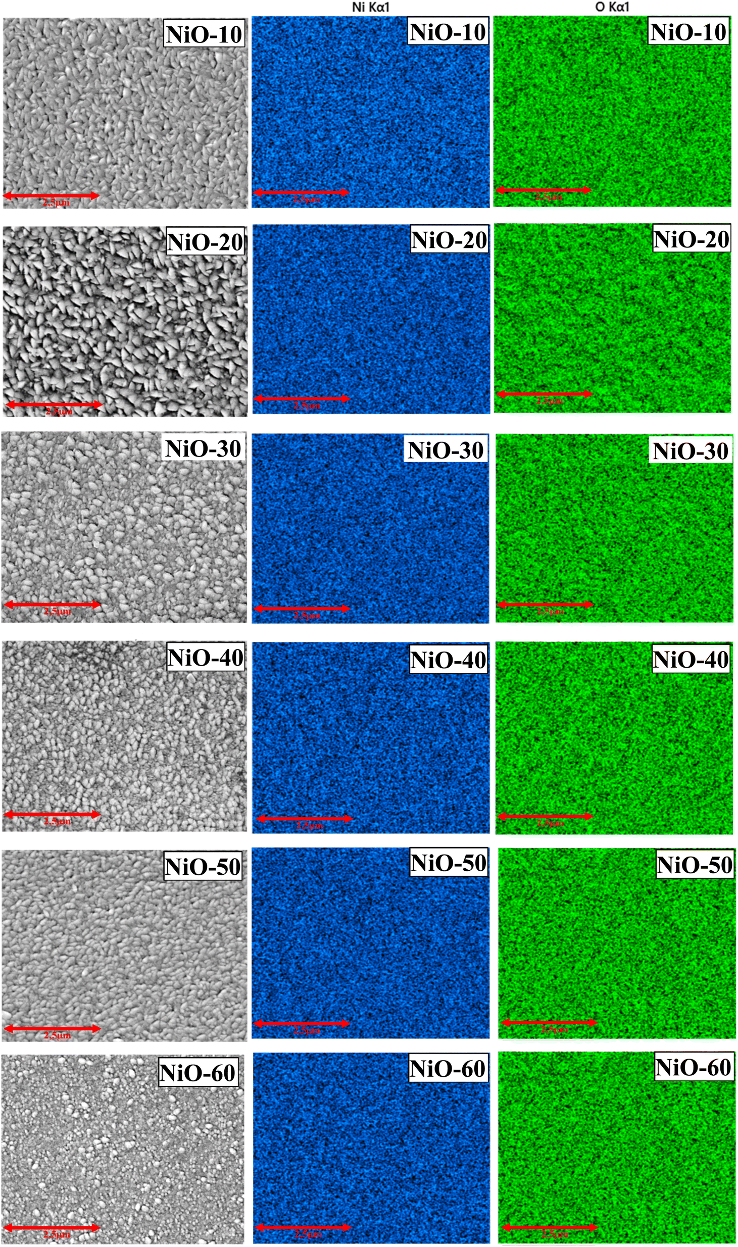
To determine the elemental composition of Ni and O in NiO films which were fabricated with O2 percentage x in sputtering mixed gas, NiO films were deposited on Si wafers to mitigate the influence of the substrate's oxygen content on the results. The EDX spectra presented in Fig. 1 indicate the binding energy peak position of O at 0.52 keV, attributed to the Kα line, while Ni exhibits Kα and Kβ lines at 7.48 keV and 8.26 keV, respectively, along with the Lα line at 0.84 keV. The diminished intensity of the Si Kα line, depicted in Fig. 1, is ascribed to the 1400 nm thickness of NiO, as demonstrated in the FESEM images in Section 3.4. The atomic content results for Ni and O are presented in Table 2, demonstrating a decrease in the Ni to O ratio r as the O2 content x (ranging from 10 to 50, in increments of 10) in the sputtering gas increases. This indicates that the concentration of Ni vacancies (VNi) rises with x, resulting in the transformation of some Ni2+ ions into Ni3+ ions in the host lattice, corresponding to the formation of VNi, which aligns with the findings in the ref. 1 and 3–5. However, when x = 60, the r ratio experiences a minor rise due to the production of the Ni2O3 phase, indicating a limitation in the contribution of interstitial oxygen for the creation of VNi which is consistent with ref. 40. Furthermore, the distribution of Ni and O across the full NiO film is entirely uniform, as seen in Fig. 2 where images were acquired at a magnification of 20![[thin space (1/6-em)]](https://www.rsc.org/images/entities/char_2009.gif) 000.
000.
 |
| | Fig. 1 EDX spectra of NiO-x films deposited with the different O2 content in a mixed sputtering gas. | |
Table 2 Atomic content of NiO-x films deposited with the different O2 content in a mixed sputtering gas
| Samples |
%at. Ni |
%at. O |
Ratio of 
|
| NiO-10 |
45.68 |
54.32 |
≈ 0.84 |
| NiO-20 |
44.79 |
55.71 |
≈ 0.80 |
| NiO-30 |
43.55 |
56.45 |
≈ 0.77 |
| NiO-40 |
42.89 |
57.11 |
≈ 0.75 |
| NiO-50 |
42.21 |
57.79 |
≈ 0.73 |
| NiO-60 |
42.98 |
58.01 |
≈ 0.74 |
 |
| | Fig. 2 EDX mapping images of NiO-x films deposited with varying O2 content in the mixed sputtering gas. Columns 1, 2, and 3 show the FESEM image used for EDX scanning, the Ni elemental mapping (blue color), and the O elemental mapping (green color), respectively. | |
3.2 Analysis of structural properties with XRD patterns
The crystal quality of NiO films deposited at varying x values is examined in Fig. 3. The NiO films, corresponding to x values ranging from 10 to 50, exhibit a predominant (200) lattice reflection alongside a weak (111) reflection, signifying the cubic phase according to JCPDS card 1049. Additionally, the presence of the Ni2O3 (002) secondary phase, as indicated in JCPDS card 0481, is observed with the prominent NiO (200) phase; however, the NiO (111) phase is absent at x = 60, as determined by XRD analysis. The results indicated that excessive O2 levels lead to the formation of the Ni2O3 (002) secondary phase. Table 3 indicates that as x increases from 10 to 20, the average crystal size expands, reflecting a trend toward reaching a standard position of the NiO (200) lattice reflection at 2θ = 43.27. As a result, the presence of VNi leads to the conversion of Ni2+ ions into Ni3+ ions, causing a shift in 2θ to a higher value, which compensates for the oxygen vacancies that remain at lower x values. When x > 20, the 2θ value of the (111) and (200) lattice reflections continues to shift to a higher position due to the increased VNi, which corresponds to the substitution of Ni2+ ions by Ni3+ ions in the host lattice. This leads to a decrease in the average crystal size, reaching a minimum of 32 nm, while maintaining sufficient crystal quality for diverse applications. The average crystal size is calculated by considering the phase weight percentage of each lattice reflection, derived from the ratio of the individual integrated intensity of each reflection to the total integrated intensity of all lattice reflections. Both the average crystal size and the 2θ value are consistent with the fluctuating trend in lattice parameters with x. The EDX study presented in Section 3.1 is supported by the XRD analysis, which demonstrates that a rise in x correlates with an increase in the amount of VNi present in the host lattice.
 |
| | Fig. 3 XRD patterns of NiO-x films deposited with the different O2 content in a mixed sputtering gas. | |
Table 3 Structural analysis results of NiO-x films deposited with the different O2 content in a mixed sputtering gas
| Samples |
Lattice reflections of NiO |
Diffractive angle 2θ (degree) |
Full width at half-maximum (degree) |
Crystalline size D (nm) |
Weight percent of phase |
Average crystalline size D (nm) |
Lattice parameters (Å) |
| NiO-10 |
NiO (111) |
37.23 |
0.25 |
33.54 |
0.24 |
42.24 |
a = 4.1843 |
| NiO (200) |
43.23 |
0.19 |
44.99 |
0.76 |
| NiO-20 |
NiO (111) |
37.31 |
0.24 |
34.95 |
0.23 |
44.61 |
a = 4.1806 |
| NiO (200) |
43.27 |
0.18 |
47.50 |
0.77 |
| NiO-30 |
NiO (111) |
37.34 |
0.29 |
28.93 |
0.20 |
38.62 |
a = 4.1741 |
| NiO (200) |
43.34 |
0.21 |
40.72 |
0.80 |
| NiO-40 |
NiO (111) |
37.39 |
0.37 |
22.68 |
0.18 |
34.58 |
a = 4.1723 |
| NiO (200) |
43.36 |
0.23 |
37.19 |
0.82 |
| NiO-50 |
NiO (111) |
37.43 |
0.39 |
21.52 |
0.16 |
33.37 |
a = 4.1705 |
| NiO (200) |
43.38 |
0.25 |
35.63 |
0.84 |
| NiO-60 |
NiO (200) |
43.41 |
0.28 |
30.55 |
0.89 |
31.97 |
a = 4.1677 |
| Ni2O3 (002) |
31.92 |
0.19 |
43.5 |
0.11 |
3.3 Analysis of surface morphology with AFM
The AFM images shown in Fig. 4 provide insight into the surface morphology of NiO films. These images reveal that the root mean square (RMS) value of the films decreases as x increases, indicating a decline in crystal quality. Notably, the NiO-20 film has the lowest RMS, reflecting its superior crystal quality. This observation aligns with the trend in average crystal size obtained through XRD analysis. In the AFM images, the grain height decreases with increasing x, requiring representation on a separate scale axis, while the color brightness axis remains constant to reflect the evolution of the RMS value. Additionally, the AFM morphology demonstrates a homogeneous grain distribution, which is beneficial for surface applications. The RMS of films varies from 8.05 to 16.44 nm, which is appropriate for SERS applications.
 |
| | Fig. 4 AFM images of NiO-x films deposited with the different O2 content in a mixed sputtering gas. | |
3.4 Analysis of surface and cross-section morphology with FESEM
FESEM morphology reveals the nanoscale grain distribution, grain shape, and film thickness, while the AFM morphology provides complementary information on surface roughness and fine morphological features at the nanoscale. Therefore, the FESEM morphology of NiO films is analyzed with respect to x, and the results are shown in Fig. 5. At x = 10, the FESEM image displays triangular prism architecture, a remarkably uniform distribution, and a predominant grain size of approximately 190 nm. Furthermore, at x = 20, the grain size increases to 200 nm or greater, resembling the coalescing of smaller triangular prisms, which signifies the grain evolution pattern as ascertained by XRD research. However, the observed reduction in grain size from 180 to 110 nm as x varies from 30 to 60 reflects the crystal grain degradation seen in the XRD analysis, indicating that the grain size fluctuations in the FESEM images are consistent with the structural characteristics revealed by both the AFM and XRD analyses. Furthermore, the grain size distribution pattern as a function of x is shown in Fig. 5, particularly in the Cross-section FESEM morphology, which clearly demonstrates the enhancement of crystal quality from the inner layer adjacent to the substrate to the uppermost surface layer. The cross-section also reveals a film thickness of approximately 1400 nm. The trends in FESEM morphology align with the results from both the XRD and AFM analyses. Furthermore, the external morphology of the FESEM grain features numerous grooves, edges, kinks, and counters that enhance the likelihood of SERS signals arising from the localized electric field.
 |
| | Fig. 5 FESEM images of NiO-x films deposited with the different O2 percent in a mixed sputtering gas. Every sample is measured at a high voltage of 3.00 kV, with a working distance of around 11 mm and an 80000 magnification. | |
3.5 Analysis of optical property with UV-vis spectra
The UV-vis absorption spectra of NiO films deposited with x, as illustrated in Fig. 6A, reveal two absorption edges for all films. The first absorption edge (edge 1) is attributed to electron transitions from the valence band to the conduction band, referred to as exciton transition absorption. The second absorption edge (edge 2) may result from electron transitions from acceptor defect energy levels situated above the valence band maximum (VBM) to conduction band. In the literature, there is no definitive information regarding this energy band, which may be VNi or Ni3+. However, the studies1,3–5 indicate that NiO deposited in an oxygen-rich atmosphere results in each VNi formation corresponding to the transfer of 2 electrons from two Ni2+ ions to VNi, resulting in the formation of Ni3+–Ni2+ substitution, as illustrated in the following equation  , where NiXNi,
  , OXO, and
  represent Ni2+, Ni3+, O2−, and VNi at lattice sites of the host lattice, respectively. It is clear that 2 electrons are positioned at VNi site, resulting in edge 2. Besides, Fig. 6B and C were derived using the Tauc plot methodology applied to the UV-vis absorption data. The absorption coefficient (α) was determined from the absorbance data using the formula α = 2.303 × A/d, where A represents absorbance and d denotes film thickness. We employed the Tauc equation to determine the optical bandgap: (αhv)2 = A(hν − Eg). For a permitted direct transition, where hν represents the photon energy and Eg denotes the optical bandgap. We graphically represented (αhν)2 against hν and extended the linear region of the curve to the energy axis (hν) at the point where (αhν)2 equals zero. The intercept provides the expected bandgap energy. Fig. 6B illustrates the main band edge utilized to determine Eg (the fundamental bandgap). Fig. 6C illustrates a secondary edge, which we attribute to a sub-bandgap transition Es, presumably resulting from localized states or defect levels. The graphs were linearly fitted at their corresponding absorption edges to determine Eg and Es, respectively. The results demonstrated that the reduction of Eg with an increase in x is attributable to the upward shift of the VBM, as mentioned in ref. 35, while the drop in Es is related to the broadening of the VNi defect energy level. The difference between Eg and Es for all films indicated that the VNi defect energy level is 0.9 eV above VBM as seen in Fig. 6D.
 |
| | Fig. 6 (A) UV-vis spectra, (B) band gap, (C) sub-bandgap, and (D) electron transition diagram of NiO-x films deposited with the different O2 percent in a mixed sputtering gas. | |
3.6 Electrical property of NiO films
The Hall measurement as resulted in Table 4 indicates that resistivity diminishes as x increases, attributed to the formation of VNi in the oxygen-rich deposition environment as indicated in Section 3.5, resulting in an increase in Ni3+ ions within the host lattice. Consequently, adjacent pairs of Ni2+and Ni3+ ions within the NiO host lattice produced a hole current analogous to that of polarons, especially under illumination. It is clear that the conductivity is mostly influenced by hole concentration, while hole mobility also has a slight effect. The hole mobility of NiO-60 diminishes due to the reduction of crystal quality, as discussed in Sections 3.2–3.4. This occurs because of the creation of the Ni2O3 phase within the host lattice when the film is produced in an oxygen-rich atmosphere. NiO-50 exhibits optimal electrical characteristics, including a resistivity of 0.44 Ω cm, hole mobility of 1.96 cm2 V−1 s−1, and hole concentration of 7.22 × 1018 cm−3. The optimal electrical characteristics represent the most advantageous combination of electrical properties, including the lowest resistivity, highest hole mobility, and largest hole concentration, among the series of NiO-x thin films formed under different O2 flow conditions. The resistivity of 0.44 Ω cm, hole mobility of 1.96 cm2 V−1 s−1, and hole concentration of 7.22 × 1018 cm−3 are the most advantageous among the analyzed samples. These electrical characteristics are deemed best for surface-enhanced Raman spectroscopy.
Table 4 The results of the Hall effect measurement of NiO-x films deposited with the different O2 percent in a mixed sputtering gas
| Samples |
ρ (Ω cm) |
μ (cm2 V−1 s−1) |
n (cm−3) |
Type |
| NiO-10 |
15.3 |
3.69 |
1.11 × 10¹⁷ |
p |
| NiO-20 |
10.8 |
4.01 |
1.45 × 10¹⁷ |
p |
| NiO-30 |
1.53 |
3.22 |
1.27 × 10¹⁸ |
p |
| NiO-40 |
1.04 |
2.54 |
2.37 × 10¹⁸ |
p |
| NiO-50 |
0.44 |
1.96 |
7.22 × 10¹⁸ |
p |
| NiO-60 |
1.00 |
0.81 |
7.68 × 10¹⁸ |
p |
3.7 Application of NiO films for surface-enhanced Raman spectroscopy
Rhodamine 6G (R6G) dissolved in water at varying concentrations is applied to NiO/glass and NiO/Si substrates for the detection of Raman signals in Surface Enhanced Raman Spectroscopy (SERS) applications. The Raman spectra of R6G on NiO/glass, specifically at a concentration of 10−5 M R6G, shown in Fig. 7A, display characteristic peaks at 612, 774, 1124, 1313, 1363, 1505, 1572, and 1651 cm−1. These characteristic peaks are consistently observed across all NiO films, with the corresponding vibrational modes outlined in Table 5, as mentioned in ref. 41–43. The Raman R6G signals are evaluated on NiO/glass, increasing with the hole concentration of NiO films, except for NiO-60 corresponding to 60% O2, due to its limited hole mobility, which diminishes electron transitions between NiO and R6G; Consequently, the enhancement of R6G Raman signals with increasing hole concentration in NiO suggests that the SERS effect is driven by a charge transfer mechanism between NiO and R6G, as illustrated in Fig. 7D. Notably, NiO-50 produces the strongest Raman signal. A comparison of R6G signals at 10−5 M between NiO-50/glass and NiO-50/Si reveals that the SERS signal for NiO-50/Si is significantly stronger than that for NiO-50/glass. This enhanced signal is attributed to hole diffusion from Si to the R6G/NiO interface, driven by the formation of a NiO/Si heterojunction. Additionally, the SERS signal for NiO-50/Si was measured at progressively lower R6G concentrations, down to 10−9 M. Despite the concentration decrease, the characteristic R6G peaks remained clearly detectable, similar to those observed at higher concentrations. The electron transition process responsible for the enhanced SERS signal is further supported by comparing the R6G signal at 10−9 M for NiO-50/Si with and without an applied voltage bias. The SERS signal for the voltage-biased sample was markedly stronger than that for the unbiased sample, as shown in Fig. 7C. This enhancement is attributed to the electron transition process between NiO and R6G, as illustrated in Fig. 7D, and the increased photocurrent generated in NiO-50/Si, as shown in Fig. 7E and F. The proposed mechanism is as follows: under laser irradiation, electron–hole pairs are generated in the depletion region at the p–n junction of NiO/n-Si. Under the influence of the built-in electric field at the junction, photogenerated holes are swiftly directed into the NiO layer. This leads to an increased hole density in the active region, enhancing the charge transfer process between the R6G molecules and the NiO material, which is a key factor in the chemical enhancement mechanism of Raman scattering. Furthermore, the electron transition mechanism shown in Fig. 7D indicates that the valence band maximum (VBM) and conduction band minimum (CBM) of NiO are derived from the bandgap of the NiO-50 film, with the VBM approximately at −5.2 eV, as reported in ref. 6, in addition to the VNi of NiO discussed in Section 3.6. Furthermore, the highest occupied molecular orbital (HOMO) and the lowest unoccupied molecular orbital (LUMO) of R6G are positioned at −5.7 eV and −3.4 eV, respectively, as cited in ref. 44 and 45. Based on this information, the energy differences between the VBM or VNi of NiO and the HOMO or LUMO of R6G are smaller than the energy of the 532 nm excitation wavelength, confirming the occurrence of an electron transfer event between NiO and R6G.
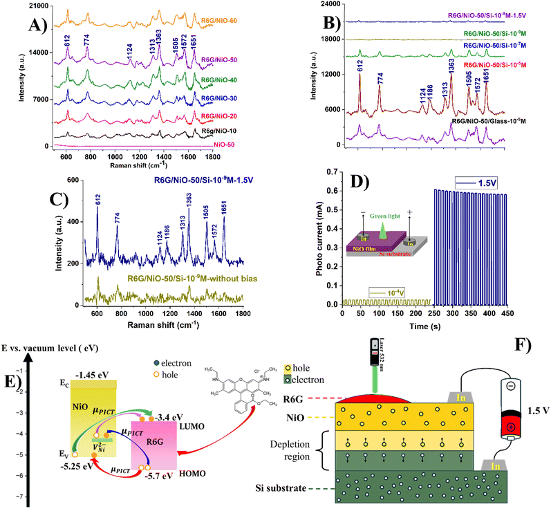 |
| | Fig. 7 Raman spectra of (A) R6G/NiO-x/glass samples at 10−5 M R6G, (B) R6G/NiO-x/Si with different R6G concentration, (C) R6G/NiO-x/Si at 10−9 M R6G without bias and with 1.5 V (data in (C) are extracted from data of (B)) applied bias as Fig. 6D, (D) I–V on–off characteristics 10−4 V and 1.5 V applied bias, (E) photo induced charge transfer enhanced Sers, and (F) Raman scattering enhanced mechanism between NiO and R6G. | |
Table 5 Raman vibrational modes of the R6G molecule
| R6G Raman shift (cm−1) |
Vibration modes |
| 612 |
C–C ring in-plane bending in xanthene/phenyl rings |
| 774 |
C–H out-of-plane bending |
| 1124 |
C–H in-plane bending in xanthene/phenyl rings |
| 1186 |
C–H in-plane bending in xanthene ring |
| 1313 |
Hybrid mode (xanthene/phenyl rings and NHC2H5 group) |
| 1363 |
C–C stretching in xanthene ring |
| 1505 |
C–C stretching in xanthene ring |
| 1572 |
C–C stretching in phenyl ring |
| 1651 |
C–C stretching in xanthene ring |
While the NiO-50 sample is emphasized in this study due to its superior SERS performance and optimal combination of structural and electronic properties, it is essential to underscore that the underlying enhancement mechanism is broadly applicable across the entire series of NiO thin films synthesized under different O2 flow rates. The proposed mechanism, which involves photo-induced charge transfer mediated by sub-bandgap energy levels introduced by nickel vacancies, is supported by consistent trends observed throughout the sample set. Notably, as the O2 content increases, systematic narrowing of the bandgap and the emergence of a distinct sub-bandgap state approximately 0.9 eV above the valence band are observed, suggesting the formation of intermediate energy states that facilitate charge transfer. Furthermore, compositional analysis reveals a progressive increase in Ni vacancy concentration and Ni3+ species, as confirmed by EDX and XPS measurements. These findings, combined with variations in surface morphology—such as reduced grain size and increased RMS roughness—indicate an enhanced density of active sites and improved molecule–semiconductor coupling. Together, these factors provide strong evidence for the universality of the proposed charge transfer-based enhancement mechanism across all samples, not solely limited to NiO-50. To quantify the Raman enhancement capability of the NiO/Si substrate, the Raman Enhancement Factor (EF) was calculated by comparing the intensity of the characteristic Raman peak at 612 cm−1 of the R6G molecule under two conditions: (i) a 10−9 M R6G solution on the NiO-50/Si substrate with a 1.5 V reverse bias, and (ii) a 1 M R6G solution on a glass substrate. As shown in Fig. 7, the signal intensity in condition (i) remains significantly high, even though the molecular concentration is 9 orders of magnitude lower than in condition (ii), emphasizing the strong enhancement effect of the material substrate. The EF is calculated using the following formula, EF = (ISERS/Iref) × (Cref/CSERS), where ISERS is the Raman peak intensity at 612 cm−1 for the 10−9 M R6G solution on the NiO/Si substrate with 1.5 V reversed bias, Iref is the Raman peak intensity at 612 cm−1 for the 1 M R6G solution on the glass substrate, CSERS is the concentration of the R6G solution in the SERS sample (10−9 M), and Cref is the concentration of the R6G solution in the reference sample (1 M). When compared to previously reported results (Table 6), the NiO/Si substrate in this study exhibits superior enhancement capability. This can be attributed to the synergistic effect of chemical enhancement mechanisms, the internal electric field at the p–n junction, and the reverse bias voltage, all of which strongly facilitate the charge transfer process. It should be noted that the EF value calculated in this study is based on analyte concentration and can be reasonably converted to be equivalent to EF values determined using molecule-counting approaches, as reported in studies.44,45,48 The exact control of measurement parameters, including laser spot diameter, analyte concentration, and sampling volume, ensures that the obtained EF value is validly comparable to those reported in the references listed in Table 6. These findings underscore the potential of NiO materials combined with p–n junction semiconductor structures in the development of high-performance SERS platforms, particularly for detecting organic molecules at ultra-low concentrations (Fig. 8).
Table 6 Comparison of the enhancement factor (EF) in this study with those reported in other works
| Substrates |
Enhancement factor (EF) |
Ref. |
| 3D hollow MoS2 |
106 |
44 |
| Cu2O/Ag |
1.4 × 10⁵ |
45 |
| PSi/Ag |
8.3 × 10⁷ |
46 |
| MoOx nanorods |
1.14 × 10⁶ |
47 |
| Ti3C2Tx/AgNPs |
3.8 × 10⁸ |
48 |
| This work |
9.6 × 10⁸ |
|
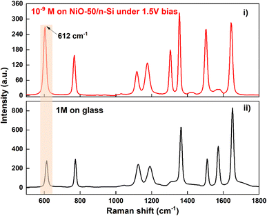 |
| | Fig. 8 The intensity of the characteristic Raman peak at 609 cm−1 of the R6G molecule measured under two conditions: (i) a 10−9 M R6G solution on the NiO-50/Si substrate under 1.5 V bias and (ii) a 1 M R6G solution NiO/glass substrate. | |
4. Conclusion
In this study, NiO films were deposited with varying O2 content in a sputtering mixed gas of Ar and O2, resulting in an increase in the concentration of Ni vacancies and Ni3+ ions in the NiO host lattice as the O2 content increased, as confirmed through energy-dispersive X-ray (EDX) analysis. The NiO film deposited with 50% O2 in the sputtering mixed gas exhibits a crystal structure with a crystallite size of 33.7 nm, an RMS roughness of 14.34 nm, and a grain size of 160 nm, as observed through FESEM imaging, making it highly suitable for Surface-Enhanced Raman Spectroscopy (SERS) applications. Despite its structural properties are not the most exceptional, it demonstrates the lowest resistivity of 0.44 Ω cm and sufficiently high hole concentration of 7.22 × 1018 cm−3, creating an optimal balance of characteristics. This balance positions NiO-50 as the most promising candidate for SERS applications among the evaluated samples. UV-vis absorption spectra reveal that the Ni vacancy energy level is located 0.9 eV above the valence band maximum, facilitating electron transitions during the SERS process. Additionally, current–voltage (I–V) characteristics, including on–off time pulse measurements, along with SERS signals recorded at a R6G concentration of 10−9 M under a 1.5 V bias, provide strong evidence for the electron transition mechanism driving the SERS effect in NiO-50. The calculated EF for the Raman signal of NiO/Si is 9.6 × 10⁸, which is higher than previously reported values.
Data availability
All data relevant for the reproduction of the results presented in this work are included within the article.
Conflicts of interest
There are no conflicts to declare.
References
- M.-C. Li, M.-J. Dai, S.-S. Lin, S.-C. Chen, J. Xu, X.-L. Liu, E.-H. Wu, A.-N. Ding, J.-H. Gong and H. Sun, Effect of annealing temperature on the optoelectronic properties and structure of NiO films, Ceram. Int., 2022, 48, 2820–2825 CrossRef CAS.
- D. Zhang, Y. Wang, Y. Wang, Y. Zhang and X.-M. Song, Fe2O3/NiO photocathode for photocatalytic methanol fuel cell: An insight on solar energy conversion, J. Alloys Compd., 2020, 815, 152377 CrossRef CAS.
- X. Yan, J. Zheng, L. Zheng, G. Lin, H. Lin, G. Chen, B. Du and F. Zhang, Optimization of sputtering NiO films for perovskite solar cell applications, Mater. Res. Bull., 2018, 103, 150–157 CrossRef CAS.
- S.-C. Chen, T.-Y. Kuo, H.-C. Lin, R.-Z. Chen and H. Sun, Optoelectronic properties of p-type NiO films deposited by direct current magnetron sputtering versus high power impulse magnetron sputtering, Appl. Surf. Sci., 2020, 508, 145106 CrossRef CAS.
- X.-Y. Zhang, C. Chen, J.-F. Zhang, Y.-J. Ruan, A. Xie, W.-Y. Wu, D.-S. Wuu, S.-Y. Lien and W.-Z. Zhu, Modulation of the conductive behavior of NiO thin film deposited by HiPIMS through varying the O2 flow ratio, Ceram. Int., 2022, 48, 34668–34677 CrossRef CAS.
- G. M. Arumugam, S. K. Karunakaran, C. Liu, C. Zhang, F. Guo, S. Wu and Y. Mai, Inorganic hole transport layers in inverted perovskite solar cells: A review, Nano Sel., 2021, 2, 1081–1116 CrossRef CAS.
- S.-K. Kim, H.-J. Seok, D.-H. Kim, D.-H. Choi, S.-J. Nam, S.-C. Kim and H.-K. Kim, Comparison of NiOx thin film deposited by spin-coating or thermal evaporation for application as a hole transport layer of perovskite solar cells, RSC Adv., 2020, 10, 43847–43852 RSC.
- Y. Zhang, S. Wang, L. Chen, Y. Fang, H. Shen and Z. Du, Solution-processed quantum dot light-emitting diodes based on NiO nanocrystals hole injection layer, Org. Electron., 2017, 44, 189–197 CrossRef CAS.
- A. A. Ahmed, M. Devarajan, M. E. Raypah and N. Afzal, Growth and characterization of NiO films on aluminum substrate as thermal interface material for LED application, Surf. Coat. Technol., 2018, 350, 462–468 CrossRef CAS.
- C. Song, G. Xiang, J. Zhang, Z. Yue, X. Zhang, B. Ding, Y. Jin, P. Wang, H. Li, H. He, L. Wang, Y. Zhao and H. Wang, Pure ultraviolet light-emitting diode based on the p-NiO/i-NiO/n-GaN structure by magnetron sputtering, Opt. Mater., 2023, 145, 114452 CrossRef CAS.
- R. Balakarthikeyan, A. Santhanam, R. Anandhi, S. Vinoth, A. M. Al-Baradi, Z. A. Alrowaili, M. S. Al-Buriahi and K. Deva Arun Kumar, Fabrication of nanostructured NiO and NiO:Cu thin films for high-performance ultraviolet photodetector, Opt. Mater., 2021, 120, 111387 CrossRef CAS.
- M. Athira, S. P. Bharath and S. Angappane, SnO2-NiO heterojunction based self-powered UV photodetectors, Sens. Actuators, A, 2022, 340, 113540 CrossRef CAS.
- R. Wen, C. G. Granqvist and G. A. Niklasson, Anodic Electrochromism for Energy-Efficient Windows: Cation/Anion-Based Surface Processes and Effects of Crystal Facets in Nickel Oxide Thin Films, Adv. Funct. Mater., 2015, 25, 3359–3370 CrossRef CAS.
- Y. Chen, Y. Sun, X. Dai, B. Zhang, Z. Ye, M. Wang and H. Wu, Tunable electrical properties of NiO thin films and p-type thin-film transistors, Thin Solid Films, 2015, 592, 195–199 CrossRef CAS.
- Y. Yokoiwa, Y. Abe, M. Kawamura, K. H. Kim and T. Kiba, Metallic-mode reactive sputtering of nickel oxide thin films and characterization of their electrochromic properties, Jpn. J. Appl. Phys., 2019, 58, 055504 CrossRef CAS.
- H. Lin, Z. Wang, Q. Han, R. Wang, L. Pan, H. Zhu, M. Wan and Y. Mai, The growth, properties and application of reactively sputtered nickel oxide thin films in all thin film electrochromic devices, Mater. Sci. Eng., B, 2021, 270, 115196 CrossRef CAS.
- Y. Ren, W. K. Chim, L. Guo, H. Tanoto, J. Pan and S. Y. Chiam, The coloration and degradation mechanisms of electrochromic nickel oxide, Sol. Energy Mater. Sol. Cells, 2013, 116, 83–88 CrossRef CAS.
- K. S. Usha, R. Sivakumar, C. Sanjeeviraja and J. Vivekanandan, Effect of substrate temperatures on structural, optical and dispersion energy parameters of RF sputtered nickel oxide thin films, Mater. Chem. Phys., 2023, 294, 127007 CrossRef CAS.
- F. Wang, J. Jia, W. Zhao, L. Zhang, H. Ma, N. Li and Y. Chen, Preparation and electrochromic properties of NiO and ZnO-doped NiO thin films, Mater. Sci. Semicond. Process., 2022, 151, 106986 CrossRef CAS.
- F. Zhao, H. He, Z. Cheng, Y. Tang, G. Li, G. Xu, Y. Liu and G. Han, Improving electrochromic performance of porous nickel oxide electrode via Cu doping, Electrochim. Acta, 2022, 417, 140332 CrossRef CAS.
- B. Brioual, H. Ghannam, Z. Rossi, A. Aouni, A. El-Habib, M. Diani, M. Addou, R. Matassa, S. Nottola and M. Jbilou, Effect of In-doping on electrochromic behavior of NiO thin films, Materialia, 2023, 30, 101832 CrossRef CAS.
- L. Gao, J. Hou, Z. Li, X. Gu, M. Huang and G. Su, Improved electrochromic performance of nickel oxide porous films by regulating their semiconductor type by titanium doping, J. Phys. Chem. Solids, 2023, 174, 111168 CrossRef CAS.
- M. M. Gomaa, M. H. Sayed, V. L. Patil, M. Boshta and P. S. Patil, Gas sensing performance of sprayed NiO thin films toward NO2 gas, J. Alloys Compd., 2021, 885, 160908 CrossRef CAS.
- K. Rajesh, N. Pothukanuri and M. V. R. Reddy, Studies on pure and Zn doped NiO nanostructured thin films for enhanced ammonia gas sensing applications, Chem. Phys. Impact., 2024, 8, 100397 CrossRef.
- H. L. S. Santos, P. G. Corradini, M. A. S. Andrade and L. H. Mascaro, CuO/NiOx thin film–based photocathodes for photoelectrochemical water splitting, J. Solid State Electrochem., 2020, 24, 1899–1908 CrossRef CAS.
- A. Pol, S. Sapakal, A. Khan and A. V. Kadam, Synthesis of NiO thin film on 304-grade stainless steel substrate for oxygen evolution reaction, Surf. Interfaces, 2023, 37, 102706 CrossRef CAS.
- S. Kandpal, I. Ezhov, M. Tanwar, D. Nazarov, D. Olkhovskii, L. Filatov, M. Yu. Maximov and R. Kumar, Plasma assisted atomic layer deposition NiO nanofilms for improved hybrid solid state electrochromic device, Opt. Mater., 2023, 136, 113494 CrossRef CAS.
- S. C. Chen, C. K. Wen, T. Y. Kuo, W. C. Peng and H. C. Lin, Characterization and properties of NiO films produced by rf magnetron sputtering with oxygen ion source assistance, Thin Solid Films, 2014, 572, 51–55 CrossRef CAS.
- K. S. Usha, R. Sivakumar, C. Sanjeeviraja and J. Vivekanandan, Effect of substrate temperatures on structural, optical and dispersion energy parameters of RF sputtered nickel oxide thin films, Mater. Chem. Phys., 2023, 294, 127007 CrossRef CAS.
- M. S. Jamal, S. A. Shahahmadi, P. Chelvanathan, H. F. Alharbi, M. R. Karim, M. Ahmad Dar, M. Luqman, N. H. Alharthi, Y. S. Al-Harthi, M. Aminuzzaman, N. Asim, K. Sopian, S. K. Tiong, N. Amin and Md. Akhtaruzzaman, Effects of growth temperature on the photovoltaic properties of RF sputtered undoped NiO thin films, Results Phys., 2019, 14, 102360 CrossRef.
- S. Elmassi, A. Narjis, L. Nkhaili, A. Elkissani, L. Amiri, S. Drissi, A. Abali, M. Bousseta and A. Outzourhit, Effect of annealing on structural, optical and electrical properties of nickel oxide thin films synthesized by the reactive radio frequency sputtering, Phys. B, 2022, 639, 413980 CrossRef CAS.
- T. Potlog, L. Ghimpu, V. Suman, A. Pantazi and M. Enachescu, Influence of RF sputtering power and thickness on structural and optical properties of NiO thin films, Mater. Res. Express, 2019, 6, 096440 CrossRef CAS.
- M. L. Grilli, F. Menchini, T. Dikonimos, P. Nunziante, L. Pilloni, M. Yilmaz, A. Piegari and A. Mittiga, Effect of growth parameters on the properties of RF-sputtered highly conductive and transparent p-type NiOx films, Semicond. Sci. Technol., 2016, 31, 055016 CrossRef.
- S. Elmassi, M. Bousseta, L. Amiri, S. Drissi, A. Abali, L. Nkhaili, A. Narjis, A. Ammar and A. Outzourhit, Effect of RF power on structural, optical and electrical properties of sputtered nickel oxide, Phys. B, 2023, 659, 414853 CrossRef CAS.
- J. Keraudy, B. Delfour-Peyrethon, A. Ferrec, J. Garcia Molleja, M. Richard-Plouet, C. Payen, J. Hamon, B. Corraze, A. Goullet and P.-Y. Jouan, Process- and optoelectronic-control of NiOx thin films deposited by reactive high power impulse magnetron sputtering, J. Appl. Phys., 2017, 121, 171916 CrossRef.
- Z. Li, Z. Ding, Z. Yan, K. Han, M. Zhang, H. Zhou, X. Sun, H. Sun, J. Li, W. Zhang and X. Liu, NiO/AgNPs nanowell enhanced SERS sensor for efficient detection of micro/nanoplastics in beverages, Talanta, 2025, 281, 126877 CrossRef CAS PubMed.
- A. Hernandez Cedillo, J. J. Velazquez Salazar, J. Mendez Lozoya, J. A. Agyei-Mensah, R. A. Guirado-López, C. Hernandez Cedillo, A. Lehr and M. Jose Yacaman, Ag@Ni–NiO NW Core–Shell Nanowires: A Reliable Surface-Enhanced Raman Scattering (SERS) Substrate, J. Phys. Chem. C, 2025, 129, 4113–4125 CrossRef CAS.
- X. Wen, Y. Liu, W. Zhang, L. You, N. Cai and J. Li, Recyclable NiO/g-C3N4/Ag hybrid substrates for sensitive SERS detection and photo-degradation of residual pesticides in beverages, Food Chem., 2025, 464, 141935 CrossRef CAS PubMed.
- P. Penila Saminy, S. Sonia, N. Dhanpal Jayram and S. Shenbagamoorthi, Unlocking the power of nano Petals: Magnifying Rhodamine 6G detection sensitivity in SERS, Inorg. Chem. Commun., 2024, 165, 112521 CrossRef CAS.
- T. K. H. Pham, B. Q. Tran, K. B. Nguyen, N. Y. N. Pham, T. H. Y. Nguyen, A. H.-T. Nguyen, N. P. Nguyen, H. D. Ngo and H. P. Pham, Oxygen partial pressure effects on nickel oxide thin films and NiO/Si diode performance, Mater. Adv., 2025, 6, 1719–1725 RSC.
- Y.-C. Liu, C.-C. Yu and S.-F. Sheu, Low concentration rhodamine 6G observed by surface-enhanced Raman scattering on optimally electrochemically roughened silver substrates, J. Mater. Chem., 2006, 16, 3546 RSC.
- C. Wu, E. Chen and J. Wei, Surface enhanced Raman spectroscopy of Rhodamine 6G on agglomerates of different-sized silver truncated nanotriangles, Colloids Surf., A, 2016, 506, 450–456 CrossRef CAS.
- S. Shim, C. M. Stuart and R. A. Mathies, Resonance Raman Cross-Sections and Vibronic Analysis of Rhodamine 6G from Broadband Stimulated Raman Spectroscopy, ChemPhysChem, 2008, 9, 697–699 CrossRef CAS PubMed.
- C. Gao, Y. Yang, H. Chen, X. Gao, X. Zhang, Z. Song, T. Zhang, K. Chen, X. Wang and Y. Han, 3D Hollow MoS2 Architecture Enabled Highly Sensitive SERS Detection, Adv. Mater. Interfaces, 2024, 2400734 Search PubMed.
- M. Zhou, X. He, L. Niu, C. Li, T. Chen and Y. Gong, Facile one−step synthesis of Ag anchoring on Cu2O for enhanced SERS activity: Efficient charge transfer and adsorption, J. Alloys Compd., 2024, 971, 172476 CrossRef CAS.
- M. Li, Y. Liu, X. Liu, Y. Zhang, T. Zhu, C. Feng and Y. Zhao, Annealing Temperature-Dependent Surface-Enhanced Raman spectroscopy on MoS2-Covered silver nanoparticle array, Spectrochim. Acta, Part A, 2022, 275, 121159 CrossRef CAS PubMed.
- T. Vo Huu, H. L. Thi Thu, L. Nguyen Hoang, K. Huynh Thuy Doan, K. N. Duy, T. D. Anh, H. Le Thi Minh, K. N. Huu and H. Le Vu Tuan, Nanorod structure tuning and defect engineering of MoOx for high-performance SERS substrates, Nanoscale, 2024, 16, 22297–22311 RSC.
- L. Li, T. Zhang, L. Zhang, G. Wang, X. Huang, W. Li, L. Wang, Y. Li, J. Li and R. Lu, Synergistic enhancement of chemical and electromagnetic effects in a Ti3C2Tx/AgNPs two-dimensional SERS substrate for ultra-sensitive detection, Anal. Chim. Acta, 2024, 1331, 343330 CrossRef CAS PubMed.
|
| This journal is © The Royal Society of Chemistry 2025 |
Click here to see how this site uses Cookies. View our privacy policy here. 
 Open Access Article
 This Open Access Article is licensed under a Creative Commons Attribution-Non Commercial 3.0 Unported Licence
 ab,
Le Huu Bao
ab,
Le Huu Bao


 , where NiXNi,
  , OXO, and
  represent Ni2+, Ni3+, O2−, and VNi at lattice sites of the host lattice, respectively. It is clear that 2 electrons are positioned at VNi site, resulting in edge 2. Besides, Fig. 6B and C were derived using the Tauc plot methodology applied to the UV-vis absorption data. The absorption coefficient (α) was determined from the absorbance data using the formula α = 2.303 × A/d, where A represents absorbance and d denotes film thickness. We employed the Tauc equation to determine the optical bandgap: (αhv)2 = A(hν − Eg). For a permitted direct transition, where hν represents the photon energy and Eg denotes the optical bandgap. We graphically represented (αhν)2 against hν and extended the linear region of the curve to the energy axis (hν) at the point where (αhν)2 equals zero. The intercept provides the expected bandgap energy. Fig. 6B illustrates the main band edge utilized to determine Eg (the fundamental bandgap). Fig. 6C illustrates a secondary edge, which we attribute to a sub-bandgap transition Es, presumably resulting from localized states or defect levels. The graphs were linearly fitted at their corresponding absorption edges to determine Eg and Es, respectively. The results demonstrated that the reduction of Eg with an increase in x is attributable to the upward shift of the VBM, as mentioned in ref. 35, while the drop in Es is related to the broadening of the VNi defect energy level. The difference between Eg and Es for all films indicated that the VNi defect energy level is 0.9 eV above VBM as seen in Fig. 6D.


