
 Open Access Article
 This Open Access Article is licensed under a Creative Commons Attribution-Non Commercial 3.0 Unported Licence
First-principles investigations of electronic property modulation in the FeCl3/MoSi2N4 heterojunction by strain, interlayer distance and vertical electric field variation†
Xinrui Chen,
Su Su,
Xuewen Wang,
Xuanyu Chen,
Syed Awais Ahmad ,
Lin Xu* and
Weibin Zhang*
,
Lin Xu* and
Weibin Zhang*
College of Physics and Electronics Information, Yunnan Key Laboratory of Opto-Electronic Information Technology, Key Laboratory of Advanced Technique & Preparation for Renewable Energy Materials-Ministry of Education, Yunnan Normal University, Kunming, 650500, P. R. China. E-mail: 220001@ynnu.edu.cn; xulin13888488199@163.com
First published on 23rd June 2025
Abstract
This study investigated the changes in the electronic properties of the FeCl3/MoSi2N4 heterostructure by modulating interlayer distance, in-plane strain, and external electric field. The results indicated that the FeCl3/MoSi2N4 van der Waals heterostructure (vdWH) is an indirect band gap semiconductor with a band gap of 1.21/2.21 eV, as determined by a PBE/HSE06 calculations, and forms a type-I heterojunction. The equilibrium interlayer distance (ΔD) is 3.35 Å and altering it results in a decrease in the band gap. Subsequently, a biaxial strain (ε) was applied to the heterostructure. With compressive strain, the band gap shows a linear decrease. When ε = −4%, the material changes from semiconductor to metallic state. Under tensile strains ranging from 1 to 3%, the band gap sharply decreases from 0.89 to 0.22 eV. Under a vertical external electric field in the −0.7 to 0.8 V Å−1 range, the band gap stabilizes at around 0.9 eV. Notably, at −0.8 V Å−1, the band gap reaches zero.
1. Introduction
Materials science is foundational in the modern industrial system, serving as the basis for all manufacturing activities and a critical driver of new technological revolutions.1,2 Therefore, developing innovative materials is essential for enhancing the efficiency and quality of manufacturing processes. Geim and Novoselov prepared monolayer graphene through mechanical exfoliation,3,4 igniting widespread interest in 2D material research. Graphene exhibits exceptional electrical conductivity, high absorption, superior carrier mobility,5 good stability, and a large surface area. Despite numerous studies focusing on large-scale production and manufacturing techniques for graphene, practical applications remain limited.6 This situation has prompted researchers to explore other 2D materials with semiconductor properties.7Subsequently, various 2D materials exhibiting excellent performance have been discovered, including g-C3N4,8 Janus MoSSe,9 and TiO2 (ref. 10 and 11) monolayers. They have shown significant progress in applications such as photocatalytic water splitting,12 degradation of organic pollutants, environmental remediation,13 and carbon dioxide reduction. Although 2D materials hold vast application potential in photocatalysis and optoelectronic devices, certain drawbacks still require optimization.
To overcome the limitations of 2D materials, van der Waals heterostructures (vdWH) demonstrate remarkable potential in modern electronics and optoelectronics, having ideal interface structure and efficient carrier separation and transport rates, flexible fabrication strategies, ultrafast bulk photovoltaic effects, and tunable band gaps.14 Various heterojunctions, such as graphene/periodic porous graphene, MoS2/WSe2, MoS2/TiO2, graphene/hexagonal boron nitride, CuInS2/ZnS,15 and g-C3N4 S-scheme heterojunctions,16 have been theoretically and experimentally studied. The successful construction of these heterojunctions indicates promising prospects for novel structures in optoelectronic devices.17,18
MoSi2N4 is a novel 2D-layered semiconductor material with unique electrical, optical, mechanical, and thermal properties. With a band gap of 1.74 eV, it falls into the category of indirect band gap semiconductors, which offer high transparency in the visible light range and demonstrate significant application potential in optoelectronics.19 However, with the development of the semiconductor industry, the requirements for semiconductor materials for photoelectric devices have become increasingly high, and thus, the improvement of the electronic and optical properties of semiconductor materials has become a continued focus of research.
The use of FeCl3 as a dopant can regulate the microstructure and electronic properties of heterojunctions.20 For example, few-layer graphene intercalated with FeCl3 has been successfully prepared. In this heterojunction, the successful doping of FeCl3 optimizes the electronic properties of the structure;21,22 the FeCl3 acts as a solid-state redox functional material doping both the graphene oxide (GO) and the single-wall carbon nanotube (SWCNT) film, resulting in a higher-conductivity composite film. As a result of doping with FeCl3, the FeCl3-GO/SWCNT/Si heterojunction achieves a higher conversion efficiency and good stability.23
Therefore, many researchers have found that constructing heterojunctions of MoSi2N4 with other 2D materials could enhance photocatalytic properties and offer possibilities in optoelectronic applications.24,25 Research indicates that the MoGe2N4/MoSi2N4 heterolayer forms a type-II band alignment, effectively promoting the separation of electrons and holes while facilitating further movement of these charge carriers.26 The MoSi2N4/GeC heterojunction possesses a stable structure, suitable band gap, strong redox potential, and high photogenerated carrier mobility. Applying strain or electric field can trigger a transition from a type-I to a type-II heterojunction,27 thereby modifying its semiconductor properties. The MoSi2N4/WO2 heterojunction demonstrates good kinetic stability and features a typical type-II band alignment. The MoSi2N4/WO2 heterojunction efficiently improves the nanoelectronic and optoelectronic applications of monolayer MoSi2N4.28 Tensile strain in the MoSe2/MoSi2N4 heterojunction can enhance light absorption in the visible region, while compressive strain improves absorption in the ultraviolet region. Positive and negative electric fields can transform the system into a type-II heterojunction, allowing for the coexistence of type-II heterojunction characteristics alongside direct band properties. These discoveries provide valuable strategies for enhancing the performance of MoSe2/MoSi2N4 heterojunctions in optoelectronic devices and expanding their application scope.29 MoSi2N4/GaN represents a direct band gap type-I heterojunction, whereas MoSi2N4/ZnO constitutes an indirect band gap type-II heterojunction. By applying an external electric field or mechanical strain in the out-of-plane direction, the band structures of MoSi2N4/GaN and MoSi2N4/ZnO can undergo significant transformations, exhibiting rich transition behaviors, including shifts from type-I to type-II band alignments and transitions from direct to indirect band gaps. These findings reveal the tremendous design flexibility of MoSi2N4 for tunable composite materials for ultra-compact optoelectronic applications.30
This study describes the novel construction of the FeCl3/MoSi2N4 vdWH by vertically stacking monolayer FeCl3 on MoSi2N4. Based on first-principles calculations, we investigate the electronic structure of FeCl3/MoSi2N4 vdWH and find that it exhibits type-I band alignment. To obtain superior characteristics in 2D materials, we systematically alter the interlayer distance, apply strain, and introduce external electric fields to modulate the electronic properties of the FeCl3/MoSi2N4 vdWH. Our research reveals that the FeCl3/MoSi2N4 vdWH possesses an indirect band gap of 1.21/2.21 eV, as given by the PBE/HSE06 calculations, and a work function of 6.08 eV, with a type-I band-edge alignment. Additionally, our findings reveal transitions between semiconductor and metal properties and type-I and type-II heterojunctions. We believe that the FeCl3/MoSi2N4 vdWH will show promising application prospects in flexible electronic devices, optoelectronics, and photocatalytic applications.
2. Computational methods
This study employs first-principles calculations based on Density Functional Theory (DFT) to investigate the geometric optimization, electronic structure, and band alignment of the FeCl3/MoSi2N4 vdWH. The calculations were performed using the Perdew–Burke–Ernzerhof (PBE) pseudopotential in the Vienna Ab initio Simulation Package (VASP), with the exchange–correlation potential optimized through the Generalized Gradient Approximation (GGA).31,32 Recognizing the systematic band gap underestimation of the PBE-GGA functionals, we adopted the HSE06 hybrid functional (Heyd–Scuseria–Ernzerhof 2006) to achieve higher-precision band structure calculations.33 The band gap data obtained using HSE06 have been included in the ESI.† At the same time, to visualize the discrepancy in band gap predictions arising from different computational algorithms, a comparative bar chart was constructed, as illustrated in Fig. S1.† Despite its tendency to underestimate absolute band gap values, the PBE functional demonstrates reliable accuracy in predicting band gap trends and elucidating underlying physical mechanisms. Notably, its computational efficiency surpasses that of HSE06, offering significant cost-effectiveness. For these combined reasons, PBE was selected for subsequent investigations of the heterostructure. For the monolayers of FeCl3 and MoSi2N4 and the hybrid FeCl3/MoSi2N4 vdWH, a cutoff energy of 450 eV was set for the electronic wave functions, along with a maximum of 100 self-consistent field repetitions. The K-point sampling in the Brillouin zone was configured to 6 × 6 × 1, while the energy convergence criterion was defined as 10−8 eV. A vacuum layer thickness of 25 Å was introduced along the Z-axis to eliminate periodic boundary interactions. Considering the van der Waals interactions arising from weak interlayer coupling, Grimme's DFT-D3 method was employed for corrections.34 During structural relaxation, the convergence thresholds for atomic energy and interatomic forces were established at 10−5 eV and 0.01 eV Å−1, respectively. For subsequent electronic property calculations, to minimize the lattice mismatch, we constructed the FeCl3/MoSi2N4 vdWH using a 1 × 1 × 1 monolayer of FeCl3 and a 2 × 2 × 1 monolayer of MoSi2N4, resulting in a calculated lattice mismatch of 1.72%.Our study employs a meticulously constructed 1 × 1 × 1 FeCl3/2 × 2 × 1 MoSi2N4 supercell to systematically investigate the electronic structure of the FeCl3/MoSi2N4 vdWH and its responses to varying interlayer distances (ΔD), in-plane strains (ε), and applied electric fields (E). To preliminarily assess supercell-dependent band gap variations, we executed full structural relaxation of an additional (2 × 2 × 1) FeCl3/(4 × 4 × 1) MoSi2N4 supercell configuration. The resultant band gap discrepancy of merely 0.03 eV and the band gaps are presented in Fig. S1.† Given that this minor discrepancy is substantially smaller than the regulatory scales studied later, and considering the prohibitive computational costs of high-precision DFT, we assert that the core physical mechanisms and modulation trends revealed in the (1 × 1 × 1) FeCl3/(2 × 2 × 1) MoSi2N4 supercell are representative within reasonable configuration limits. All subsequent calculations regarding interlayer spacing, biaxial strain, and vertical electric field effects were, therefore, performed exclusively on this supercell.
Initially, we explored the influence of interlayer distance on the electronic structure of the FeCl3/MoSi2N4 vdWH, selecting an interlayer distance range from 1.5 to 6 Å. Subsequently, we applied in-plane strains ranging from −4 to 5% and external electric fields of −0.8 to 0.8 V Å−1 to the FeCl3/MoSi2N4 vdWH. Mechanical strains can be categorized into uniaxial and biaxial strains. The strain was calculated using the following formula:
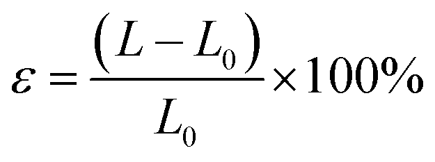 | (1) |
In eqn (1), L represents the lattice constant under strain, while L0 denotes the lattice constant without strain. When ε > 0, it indicates tensile strain, whereas ε < 0 signifies compressive strain, with a variation magnitude of 1%. In subsequent calculations of the electronic structure of the FeCl3/MoSi2N4 vdWH, we controlled the ΔD within the range of 2.95 to 5.00 Å, applied ε values ranging from −4 to 4%, and introduced E strengths from −0.8 to 0.8 V Å−1.
The work functions of the FeCl3 and MoSi2N4 monolayers, plus the FeCl3/MoSi2N4 vdWH, define the energy barrier for electron emission from the Fermi level to vacuum. These values serve as intrinsic references for band alignment, formally expressed as:
| Φ = Evac − EF | (2) |
We calculated the vacuum level and work function for the monolayer FeCl3 using VASP, resulting in values of 1.86 eV and 6.23 eV, respectively. The vacuum level and work function of MoSi2N4 were determined to be 6.93 eV and 5.16 eV,34 respectively, consistent with previous research. The vacuum level and work function of the FeCl3/MoSi2N4 vdWH were found to be 7.67 eV and 6.08 eV, respectively. Using eqn (2), we calculated the Fermi levels of the monolayers: −4.37 eV for FeCl3, 1.77 eV for MoSi2N4, and 1.59 eV for the FeCl3/MoSi2N4 vdWH.
3. Results and discussion
3.1 Atomic geometries and stability of the FeCl3/MoSi2N4 vdWH
To comprehensively study the FeCl3/MoSi2N4 vdWH, we first optimized the geometric structures of the monolayers of FeCl3 and MoSi2N4 and investigated their electronic properties. The top and side views of the atomic structure of the 2D monolayer FeCl3 are shown in Fig. 1(a). Each unit cell of the FeCl3 monolayer contains eight atoms, comprising two Fe atoms and six Cl atoms, with covalent bonds formed between them. After geometric optimization, the calculated lattice parameters for the 1 × 1 × 1 FeCl3 unit cell were found to be a = b = 5.91 Å, and the Fe–Cl bond length was measured to be 2.27 Å. For the 1 × 1 × 1 MoSi2N4 unit cell, the calculated lattice parameters were a = b = 2.90 Å,35 which aligns with previously reported values. Due to the differing lattice parameters between the FeCl3 and MoSi2N4 monolayers, the construction of a supercell was required. To successfully create this supercell, we utilized a 2 × 2 × 1 MoSi2N4 unit cell; the corresponding top and side views of the atomic structure are displayed in Fig. 1(b). Each unit cell of MoSi2N4 contains twenty-eight atoms, including four Mo atoms, eight Si atoms, and sixteen N atoms, with covalent bonds formed among them. Following geometric optimization, the calculated lattice parameters for MoSi2N4 were determined to be a = b = 5.81 Å. The Mo–N bond length was measured to be 2.09 Å, the N–Si bond length was 1.75 Å, and the Si–Mo bond length was 3.43 Å, all of which are consistent with data from other reports.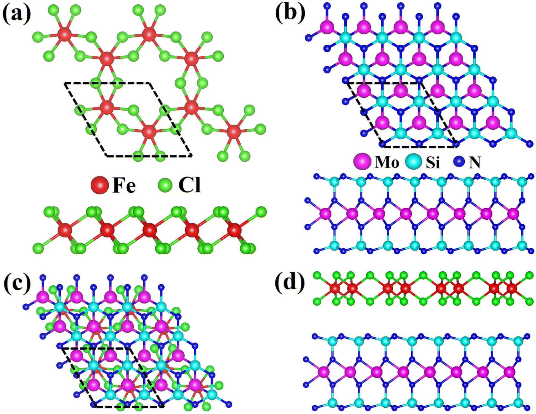 | ||
| Fig. 1 (a) Top view and side view of the optimized atomic structure of the FeCl3 monolayer. (b) Top view and side view of the optimized atomic structure of the MoSi2N4 monolayer. (c) Top view and (d) side view of the optimized atomic structure of the FeCl3/MoSi2N4 vdWH. Magenta, cyan, blue, red, and green balls represent molybdenum, silicon, nitrogen iron and chlorine atoms. | ||
The top view of the atomic structure of the FeCl3/MoSi2N4 vdWH is presented in Fig. 1(c), while the side view is shown in Fig. 1(d). Each unit cell of the FeCl3/MoSi2N4 vdWH contains thirty-six atoms, consisting of two Fe atoms, six Cl atoms, four Mo atoms, eight Si atoms, and sixteen N atoms, with covalent bonds formed within the layers. As illustrated in Fig. 1(d), no covalent bonds are formed between the layers; rather, these surface layers are stacked through weak van der Waals forces. After geometric optimization, the calculated lattice parameters for the FeCl3/MoSi2N4 vdWH were found to be a = b = 5.91 Å. The Fe–Cl bond length was measured to be 2.27 Å, the Mo–Si bond length was 3.43 Å, the Mo–Fe bond length was 8.32 Å, the Mo–N bond length was 2.10 Å, and the N–Si bond length was 1.77 Å.
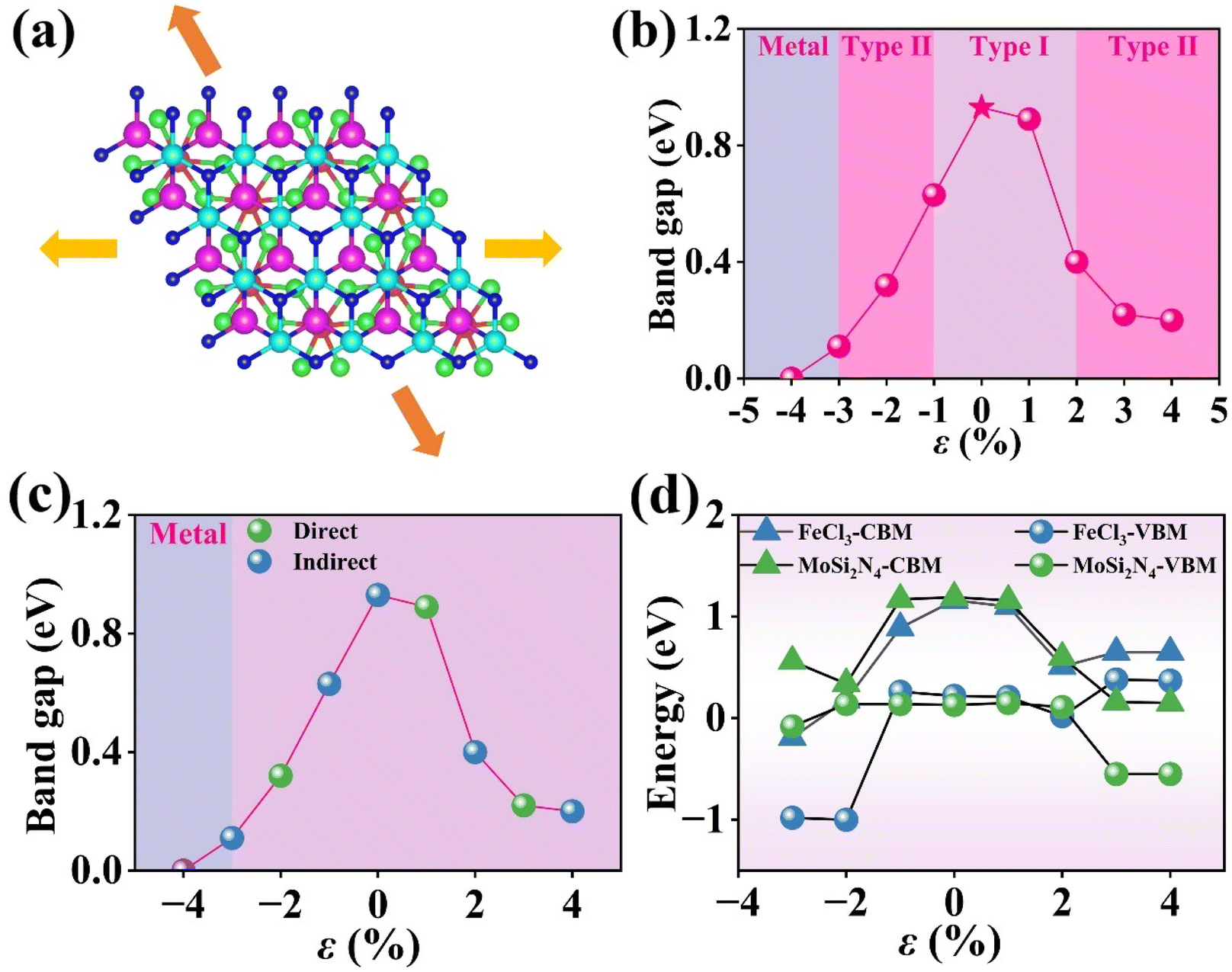
Moreover, recognizing that stacking configurations critically govern material stability, we designed four distinct heterostructures through lateral displacement of the FeCl3 monolayer relative to a fixed MoSi2N4 monolayer. As shown in Fig. 2(a), this stacking structure deliberately avoided atomic registry engineering, maintaining the naturally formed stacking architecture, as described above. This unmodified stacking arrangement preserves the intrinsic interlayer charge transfer characteristics governed by van der Waals interactions. The other stacking configurations featured vertical alignment between Fe and Mo atoms (Fig. 2(b)), between Cl and N atoms (Fig. 2(c)), or between Fe and Si atoms (Fig. 2(d)). All four structures underwent comprehensive structural relaxation to achieve fully optimized atomic positions and lattice parameters.
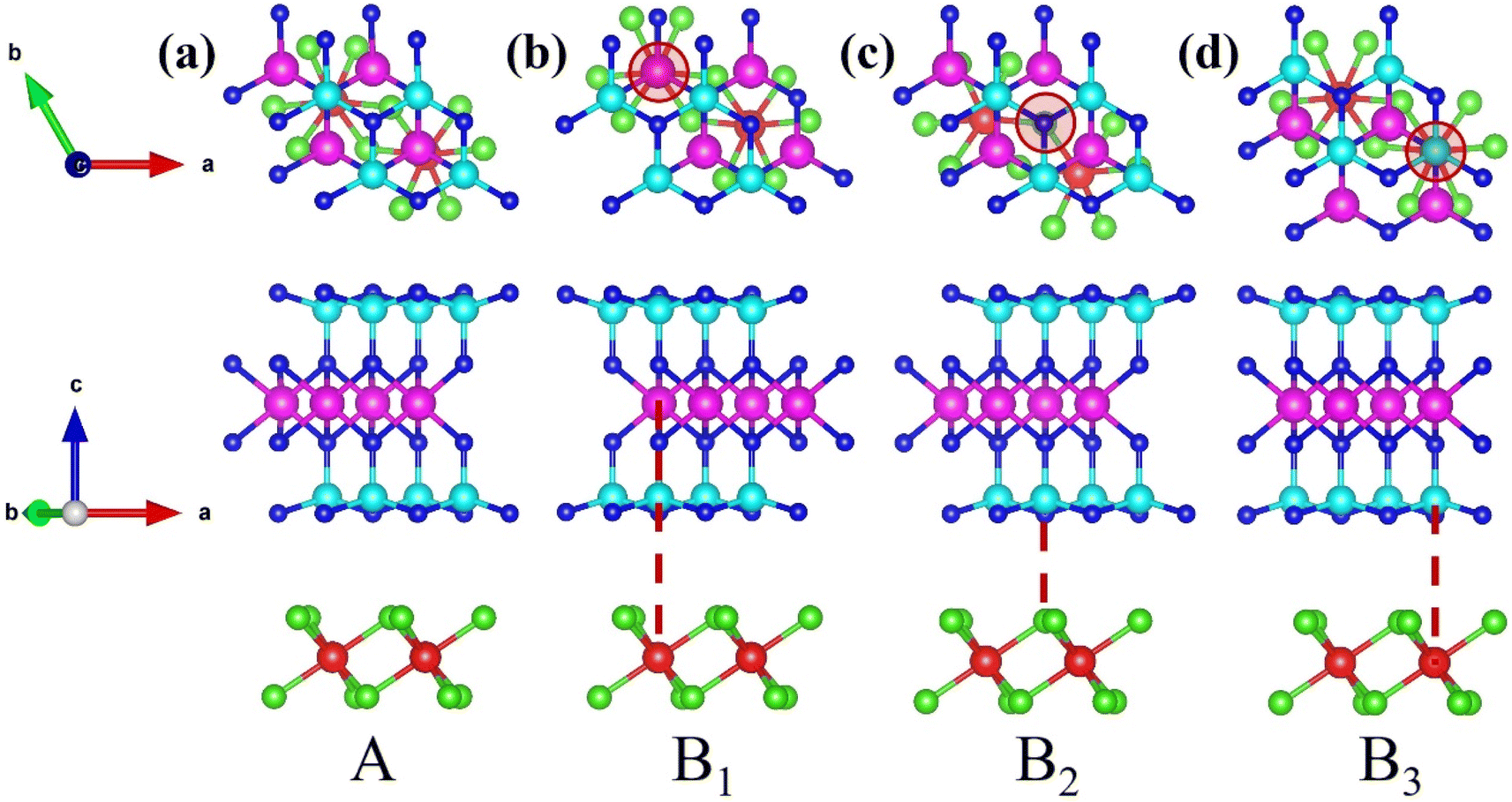 | ||
| Fig. 2 Top view and side view of the optimized FeCl3/MoSi2N4 vdWH: (a) A stacking, (b) B1 stacking, (c) B2 stacking, and (d) B3 stacking. | ||
To evaluate the stability of these heterostructures, we calculated the binding energy (Eb) for the four stacking structures. Our systematic DFT computations demonstrate that the four distinct stacking configurations exhibit binding energies of −5.81, −5.38, −5.74 and −5.77 eV, accompanied by corresponding band gap values of 0.93, 0.94, 0.93, and 0.96 eV, respectively. Collectively demonstrating robust stability, all structures show nearly identical band gaps, which indicates that the stacking structures have a negligible effect on the band gap across configurations. However, the binding energy of structure A is measurably lower than those of structures B1–B3, establishing it as the most stable structure. The calculation formulas for binding energy and cohesive energy are as follows:40
| Eb = ET − EMSN − EFC | (3) |
Dynamic stability was verified via phonon dispersion calculations across the entire Brillouin zone, as illustrated in Fig. 3(a). The absence of imaginary frequencies in all phonon branches confirms the dynamic stability of the FeCl3/MoSi2N4 vdWH.
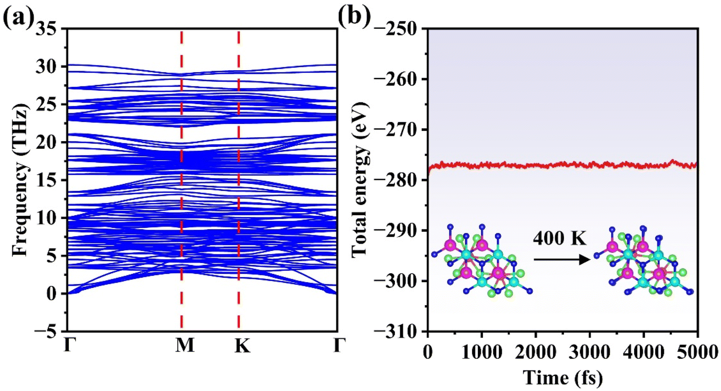 | ||
| Fig. 3 (a) Phonon spectrum of the A stacking structure and (b) evolution of the total energy of the A stacking structure during AIMD simulations at 400 K. The inset in (b) shows the atomic structure of the A stacking configuration at the end of the AIMD simulation. | ||
Additionally, our assessment of the thermal stability in the A stacking configuration at 400 K, conducted via atomic-scale molecular dynamics (AIMD) simulations (Fig. 3(b)), employed a 4000 fs trajectory with 1 fs time steps. The AIMD results reveal no evidence of structural degradation in the FeCl3/MoSi2N4 vdWH at this temperature, confirming its robust thermal stability under ambient conditions. Consequently, the A stacking configuration maintains exceptional structural integrity. Based on these findings, we selected this architecture for subsequent investigations.
3.2 Electronic structure of the FeCl3/MoSi2N4 vdWH
We then calculated the band structures for the FeCl3 monolayer, MoSi2N4 monolayer, and FeCl3/MoSi2N4 vdWH. Fig. 4(a) displays the band structure of monolayer FeCl3, in which the conduction band minimum (CBM) is located at the M-point, and the valence band maximum (VBM) is also situated at the M-point in the Brillouin zone. The CBM and VBM coincide, which indicates that FeCl3 is a direct band gap semiconductor with a band gap of 1.21/2.75 eV. | ||
| Fig. 4 Band structure of state for the (a) FeCl3 monolayer, (b) MoSi2N4 monolayer and (c) FeCl3/MoSi2N4 vdWH. (d) Weighted band structure of the FeCl3/MoSi2N4 vdWH. The Fermi level is set to zero. | ||
Fig. 4(b) illustrates the band structure of MoSi2N4. The CBM is located at the K-point, while the VBM is at the Γ point. As the CBM and VBM do not occupy the same point in the Brillouin zone, MoSi2N4 is an indirect band gap semiconductor with a band gap of 1.79/2.35 eV,35 consistent with previous reports. Additionally, the Fermi level of MoSi2N4 is close to the VBM, indicating a relatively high concentration of holes and fewer electrons in the conduction band. Hence, holes are the primary charge carriers in the conductivity process, confirming that MoSi2N4 is a p-type semiconductor.
Fig. 4(c) presents the FeCl3/MoSi2N4 vdWH band structure, in which the CBM is positioned at the K-point in the Brillouin zone and the VBM at the M-point. Upon the formation of a heterojunction between FeCl3 and MoSi2N4, electrons transfer from the conduction band of MoSi2N4 to the conduction band of FeCl3, while the holes migrate from the valence band of MoSi2N4 to the valence band of FeCl3. Consequently, the CBM of FeCl3 dominates the conduction band alignment of the heterojunction due to its lower energy level, while the VBM of FeCl3 governs the valence band alignment, owing to its higher energy level. Crucially, electron transitions still require overcoming the momentum mismatch between the M-point and K-point in the Brillouin zone, indicating that the FeCl3/MoSi2N4 vdWH is an indirect band gap semiconductor with a band gap of 1.21/2.21 eV, which is smaller than that of MoSi2N4, suggesting improved electronic properties. The Fermi level penetrating into the valence band signifies a degenerate semiconductor state at the interface, exhibiting quasi-metallic conductivity. The underlying mechanism arises from strong interfacial coupling, inducing substantial charge redistribution. This charge transfer generates exceptionally high effective hole concentrations, leading to heavy doping degeneracy in the localized interfacial region. Under degenerate conditions, the dense hole population partially fills the VBM, pinning the Fermi level within the valence band. These partially filled states confer metal-like high conductivity, while fundamentally retaining a semiconducting character—distinct from conventional metals with fully overlapping bands.
Furthermore, based on the projected band structure of the FeCl3/MoSi2N4 vdWH shown in Fig. 4(d), we find that the monolayer FeCl3 primarily contributes the VBM and CBM. Thus, the FeCl3/MoSi2N4 vdWH exhibits a type-I band alignment, which hinders the separation of electrons and holes and suppresses their transport within the heterostructure. However, this alignment is characterized by high carrier recombination efficiency, indicating that photogenerated electrons and holes are confined within the same region. This overlap of electrons and holes facilitates radiative recombination and is advantageous for light-emitting applications.36
The reduced band gap in the FeCl3/MoSi2N4 vdWH compared with that of monolayer MoSi2N4 implies a broader optical absorption spectrum. A comparative optical absorption analysis is detailed in the ESI, as illustrated in Fig. S4.†
In addition to studying the band structure, we investigated the total density of states (DOS) and the partial density of states (PDOS) for the FeCl3 monolayer, MoSi2N4 monolayer, and FeCl3/MoSi2N4 vdWH. Fig. 5(a) shows the total DOS and PDOS of the FeCl3 monolayer. Within the energy range of −1 to 0 eV, the valence band edge (VBE) is primarily derived from the contributions of the Fe 3d states. In the energy range of 0 to 2 eV, the conduction band edge (CBE) is also mainly sourced from the contributions of the Fe 3d states. Overall, the bands near the Fermi level are predominantly contributed by the Fe 3d orbitals, while the contributions from the Cl 3p orbitals are relatively minor.
 | ||
| Fig. 5 DOS of the (a) FeCl3 monolayer, (b) MoSi2N4 monolayer and (c) FeCl3/MoSi2N4 vdWH. The Fermi level is set to zero. | ||
Fig. 5(b) depicts the total DOS and PDOS of the MoSi2N4 monolayer. In the energy range of −2 to 0 eV, the VBE is mainly attributed to contributions from the Mo 4d states. In the energy range of 0 to 3 eV, the CBE is likewise primarily derived from the Mo 4d states. Thus, the bands near the Fermi level in this material are predominantly influenced by the Mo 4d orbitals, whereas the contributions from the Si 3p and N 2p orbitals are comparatively small.
Fig. 5(c) illustrates the total DOS and PDOS of the FeCl3/MoSi2N4 vdWH. Within the energy range of −1 to 0 eV, the VBE is primarily sourced from the Fe 3d states. In the energy range of 0 to 2 eV, the CBE results mainly from the hybridization between the Fe 3d and Cl 3p orbitals, with no contribution from MoSi2N4 at the band edges. The Fe 3d orbitals chiefly contribute the bands near the Fermi level, while contributions from the Cl 3p, Mo 4d, Si 3p, and N 2p orbitals are minimal.
Following the establishment of the band structure and DOS distribution of the material, subsequent analysis of carrier concentration was critical. First, electrons inherently conform to the Fermi–Dirac distribution statistics as fermionic particles:
 | (4) |
At room temperature (T = 300 K), where k0 denotes the Boltzmann constant, the net carrier concentration in a semiconductor is defined as the sum of electron and hole concentrations: nnet = n + p, with EF representing the Fermi energy at this specific temperature. At thermal equilibrium, the equilibrium electron concentration in the conduction band, denoted as n0, and the equilibrium hole concentration in the valence band, denoted as p0, are governed by the following expressions.
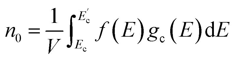 | (5) |
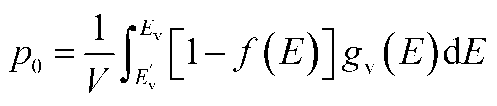 | (6) |
 , EC, EV, and
  denote the energy levels at the conduction band maximum, CBM, VBM, and valence band minimum, respectively. The functions gc(E) and gv(E) correspond to the DOS in the vicinity of the CBE and VBE.
In this way, we obtained the carrier densities from the calculated electronic structures. Through rigorous computational analysis, we determined that the heterostructure exhibits a net carrier concentration of 5.15 × 1014 cm−2, with hole and electron concentrations quantified as 4.46 × 10¹⁴ and 6.87 × 1013 cm−2, respectively. The Fermi level being located within the valence band signifies the onset of a degenerate regime in the semiconductor, where the hole concentration becomes overwhelmingly dominant (10 times greater than the electron concentration). This behavior aligns with characteristic features of heavily doped p-type semiconductors.
3.3 Work functions of the FeCl3/MoSi2N4 vdWH
The work function (Φ) corresponds to the minimum energy barrier for electron emission from the Fermi energy to the vacuum level. When constructing a vdWH from two different materials, electrons will flow from the material with a smaller work function to the one with a larger work function, thereby aligning their Fermi levels.37,38 To analyze the charge distribution in the FeCl3/MoSi2N4 vdWH, we obtained the work functions of the FeCl3 monolayer, MoSi2N4 monolayer, and FeCl3/MoSi2N4 vdWH, as shown in Fig. 6(a)–(c). The work function of the FeCl3 monolayer is 6.23 eV, which is higher than that of the MoSi2N4 monolayer at 5.16 eV. The work function of the FeCl3/MoSi2N4 vdWH is 6.08 eV, positioned between those of the FeCl3 and MoSi2N4 monolayers. | ||
| Fig. 6 Electrostatic potential curves of the (a) FeCl3 monolayer, (b) MoSi2N4 monolayer and (c) FeCl3/MoSi2N4 vdWH along the Z direction. The Fermi level and vacuum level are denoted by the long blue and red dashed lines, respectively. (d) Band alignment of FeCl3/MoSi2N4 vdWH before and after forming the contact. | ||
As the FeCl3 monolayer has a greater work function than the MoSi2N4 monolayer, when the FeCl3/MoSi2N4 vdWH is formed, electrons diffuse from the MoSi2N4 monolayer to the FeCl3 monolayer. This results in a significant number of holes being left behind in the MoSi2N4 monolayer, while a large number of electrons accumulate in the FeCl3 monolayer. Consequently, the Fermi level of the FeCl3 monolayer experiences a negative shift of 0.15 eV, while that of the MoSi2N4 monolayer shifts positively by 0.92 eV, until both Fermi levels align at the same position. Using the vacuum level (Evac) as the energy reference (0 points), we determined the FeCl3/MoSi2N4 vdWH band alignment. As illustrated in Fig. 6(d), we compared the position for the FeCl3/MoSi2N4 vdWH with those of the isolated FeCl3 and MoSi2N4 monolayers.
The FeCl3/MoSi2N4 vdWH exhibits a type-I band alignment, which is consistent with the above DOS, indicating that electrons and holes are confined within the same layer. In the FeCl3/MoSi2N4 type-I heterojunction structure, as both the CBM and VBM originate from the FeCl3 monolayer, there is no need for electrons to transfer to the MoSi2N4 monolayer during electronic transitions. This implies that both electrons and holes can migrate from the MoSi2N4 monolayer to the FeCl3 monolayer, facilitating the formation of electron–hole pairs. Furthermore, this indicates that the FeCl3/MoSi2N4 vdWH possesses excellent electron transport properties, suggesting high photoelectric conversion efficiency, making it suitable for applications in optoelectronic devices, such as light-emitting diodes and lasers.
3.4 Charge density difference of the FeCl3/MoSi2N4 vdWH
Additionally, to further analyze the charge distribution in the FeCl3/MoSi2N4 vdWH, we calculated the charge density difference. Fig. 7(a) displays the plane-averaged charge density difference of the FeCl3/MoSi2N4 vdWH, illustrating variations in charge density along the Z direction. Positive values (yellow regions) indicate electron accumulation, while negative values (cyan regions) represent electron depletion. As depicted in Fig. 7(b), the formation of regions with electron accumulation (yellow areas) and depletion (cyan areas) signifies that the FeCl3/MoSi2N4 vdWH undergoes charge redistribution to achieve interfacial charge balance. | ||
| Fig. 7 (a) Plane-averaged and (b) three-dimensional charge density differences of FeCl3/MoSi2N4 vdWH. Red, green, magenta, pink and blue balls represent the iron, chlorine, molybdenum, silicon, and nitrogen atoms, respectively. | ||
Significantly, the top layer of the FeCl3 monolayer has a prominent yellow region, indicating electron accumulation, while the lower part of the MoSi2N4 monolayer mostly exhibits cyan, signifying electron depletion. Consequently, electrons mostly migrate from the MoSi2N4 monolayer to the FeCl3 monolayer, consistent with the band alignment findings shown in Fig. 6(d).
Moreover, charge redistribution mostly occurs between the FeCl3 monolayer and the FeCl3/MoSi2N4 vdWH, while the changes in electronic charge inside the MoSi2N4 monolayer are negligible. This phenomenon is caused by the weak van der Waals interactions between the FeCl3 and MoSi2N4 monolayers, which enable the localization or redistribution of charges at the interface.
3.5 Tuning the electronic structure through interlayer distance
To determine the influence of interlayer distance on the band gap and structure of the FeCl3/MoSi2N4 vdWH, we fixed the MoSi2N4 monolayer and vertically adjusted the position of the FeCl3 monolayer to modify the heterojunction distance, as depicted in Fig. 8(a). Experimentally, the interlayer distance in 2D-material-based heterostructures can be controlled by applying pressure using the tip of a scanning tunneling microscope.39 The relationship between the band gap of the FeCl3/MoSi2N4 vdWH and the interlayer distance is illustrated in Fig. 8(b). | ||
| Fig. 8 (a) Schematic model of applied strain along the z direction. (b) Change in the band gap of the FeCl3/MoSi2N4 vdWH as a function of interlayer coupling with changing the interlayer distance. DOS of FeCl3/MoSi2N4 vdWH for interlayer distances of (c) 2.00 and (d) 2.65 Å . | ||
Initially, the equilibrium interlayer distance, which is represented as ΔD, was 3.35 Å. When ΔD was increased from 3.35 to 5.00 Å, the band gap decreased from 0.93 to 0.52 eV. Subsequently, when ΔD reached 6 Å, the band gap stabilized at 0.50 eV. Conversely, when ΔD was decreased from 3.35 to 2.00 Å, the band gap experienced a significant drop from 0.93 to 0.21 eV. Finally, reducing ΔD further from 2.00 to 1.50 Å resulted in the band gap diminishing to 0 eV. When the interlayer spacing of the heterojunction changes, the strength of the van der Waals forces also changes, leading to alterations in the interlayer interactions within the heterojunction, which in turn affects the variation in the band gap. The significance of this finding lies in revealing the nonlinear relationship between band gap evolution and interlayer distance variation. Notably, when the interlayer distance change exceeds 4.5 Å, the rate of band gap reduction slows significantly. With increasing overlap, the band gap diminishes, eventually reaching zero, indicating that the FeCl3/MoSi2N4 vdWH transitions from a semiconductor to a metal.
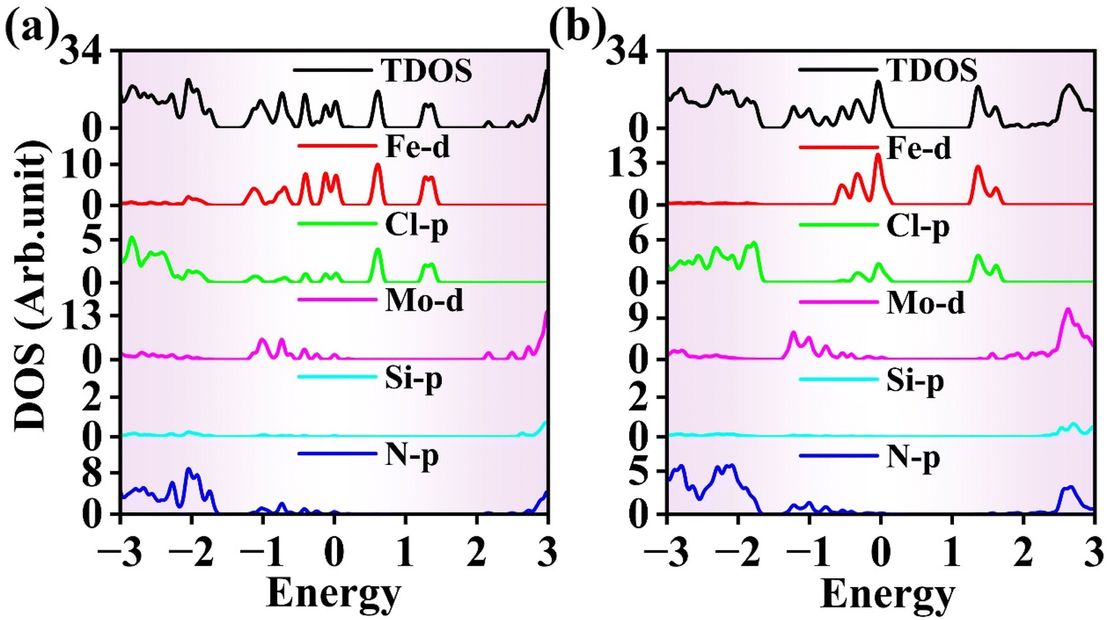
Fig. 8(c) shows the DOS at ΔD = 2.00 Å. From the figure, it can be observed that the VBE is provided by the Mo 4d orbitals in the MoSi2N4 monolayer, while the CBE is contributed by the Fe 3d orbitals in the FeCl3 monolayer. Therefore, the FeCl3/MoSi2N4 vdWH exhibits a type-II band alignment. Fig. 8(d) presents the DOS at ΔD = 2.65 Å; it can be seen that both the VBE and CBE are provided by the Fe 3d orbitals in the FeCl3 monolayer, indicating a type-I band alignment. Similarly, using differential DOS plots, we conclude that the FeCl3/MoSi2N4 vdWH displays type-II band alignment at ΔD = 2.00, 5.00, and 5.50 Å. In contrast, the FeCl3/MoSi2N4 vdWH exhibits type-I band alignment at ΔD = 2.95, 3.35, 3.92, and 4.40 Å.
3.6 Effects of tension and compression on electronic structure
Applied strain may significantly modify the band structure of the FeCl3/MoSi2N4 vdWH. This approach enhances basic scientific research in semiconductor technologies and promotes numerous practical applications in daily life, covering multiple fields from electronic devices to innovative energy solutions. These technical developments improve device efficiency and effectiveness, providing simplicity and innovation in our lives.Mechanical strain encompasses both biaxial and uniaxial strain,40 with this work primarily focusing on biaxial strain. We chose to focus on biaxial strain for three reasons: (i) theoretical perspective: biaxial strain preserves the in-plane symmetry of the system, avoiding anisotropic band renormalization induced by uniaxial strain. (ii) Experimental feasibility: uniform in-plane strain within heterostructures can be effectively achieved through biaxial pre-stretching techniques using flexible substrates, which is a well-established methodology in strain engineering practices. (iii) Heterostructure compatibility: the uniform and symmetric nature of biaxial strain enables coordinated interlayer deformation within heterostructures. In contrast, uniaxial strain introduces directional constraints that frequently lead to interlayer misalignment and subsequent failure in strain transfer, particularly in van der Waals heterostructures.
Fig. 9(a) illustrates the direction and angle of the applied strain on the FeCl3/MoSi2N4 vdWH, with the orientations being horizontal and diagonally downward and upward at a 60° angle to the vertical.
 | ||
| Fig. 9 (a) Schematic model of applied in-plane strain. (b) Variation of the band gap of FeCl3/MoSi2N4 vdWH as a function of in-plane strain. (c) Nature of the band gap and (d) shifts in band-edge alignment under applied strain for the FeCl3/MoSi2N4 vdWH. | ||
Fig. 9(b) illustrates the correlation between the applied strain and the band gap. In this study, we calculated the variation of the band gap of the FeCl3/MoSi2N4 vdWH under biaxial strain ranging from −4 to 4%. When the strain is increased from 0 to 4%, the band gap significantly decreases from 0.93 to 0.20 eV. Conversely, when the strain is decreased from zero to −3%, the band gap exhibits a nearly linear decline, dropping from 0.93 to 0.11 eV. However, as the strain decreases from −3 to −4%, the band gap reaches zero. This phenomenon is due to lattice distortion caused by the applied strain, leading to band bending that causes the CBM and VBM to move closer together, or even overlap, resulting in a band gap of zero. The transition of the FeCl3/MoSi2N4 vdWH to a band gap of zero marks its transformation from a semiconductor to a metal. Based on the DOS results, the FeCl3/MoSi2N4 vdWH changes from type-I to type-II heterojunction at ε = −3, −2, 2, 3 and 4%, as illustrated in Fig. 9(b).
Fig. 9(c) demonstrates the reversible indirect-to-direct band gap evolution in the heterostructure under biaxial strain. Under conditions of zero strain, as well as at −3, −1, 2 and 4% applied strain, electrons transfer from the higher energy state in the conduction band to the CBM, while holes migrate from the lower energy state in the valence band to the VBM, as the CBM and VBM reside at different points in the Brillouin zone. Moreover, electron transitions require overcoming the momentum mismatch between the M-point and K-point in the Brillouin zone, which indicates that the FeCl3/MoSi2N4 vdWH is an indirect band gap semiconductor. In contrast, under conditions of −2, 1 and 3% applied strain, the VBM and VBM coincide at the same high-symmetry point in the Brillouin zone, enabling direct electron transitions without requiring phonon assistance, which indicates that the FeCl3/MoSi2N4 vdWH is a direct band gap semiconductor.
To elucidate the strain-induced band gap modulation mechanism, we analyzed the band-edge evolution in the FeCl3/MoSi2N4 vdWH under biaxial deformation. These strain responses are graphically represented in Fig. 9(d). Within the −1 to +1% biaxial strain range, the heterostructure undergoes elastic lattice deformation, in which the band edges of FeCl3 and MoSi2N4 exhibit quasi-rigid shifting, resulting in minimal band gap variation. Beyond the critical ± 1% strain threshold, inelastic lattice distortion occurs, triggering significant bond-angle distortions and interlayer coupling reconstruction. This induces asynchronous and pronounced shifts in the band edges of both materials, ultimately leading to substantial band gap modifications.
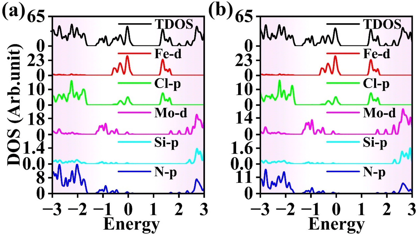
Fig. 10(a) shows the DOS at ε = −2%. It can be observed that the VBE is provided by the Mo 4d orbitals in the MoSi2N4 monolayer, while the Fe 3d orbitals in the FeCl3 monolayer contribute to the CBE. Thus, the FeCl3/MoSi2N4 vdWH exhibits a type-II band alignment. Fig. 10(b) depicts the DOS at ε = 0, in which both the valence and conduction band edges are provided by the Fe 3d orbitals in the FeCl3 monolayer, indicating that the FeCl3/MoSi2N4 vdWH has a type-I band alignment at this strain level.
 | ||
| Fig. 10 DOS of FeCl3/MoSi2N4 vdWH under in-plane strain of (a) −2 and (b) 0%. | ||
However, in experimental settings, uniaxial strain is typically more feasible for 2D materials. Consequently, we undertook complementary scrutiny of uniaxial strain effects to achieve a comprehensive understanding of strain engineering in the FeCl3/MoSi2N4 vdWH. Uniaxial strain analysis is provided in the ESI† to enable a more effective comparative evaluation. Fig. S3(a)† illustrates the direction of the uniaxial strain applied to the FeCl3/MoSi2N4 vdWH along the horizontal axis. Fig. S3(b)† illustrates the correlation between the applied uniaxial strain and the band gap. Fig. S3(c)† shows the DOS at ε = 3%, at which the FeCl3/MoSi2N4 vdWH exhibits a type-II band alignment. Additionally, Fig. S3(d)† shows the DOS at ε = 4%, at which the FeCl3/MoSi2N4 vdWH exhibits a type-I band alignment.
3.7 Relationship between applied electric field and electronic structure
The electronic structure and efficacy of semiconductor heterojunctions under an electric field are essential to their practical application. Fig. 11(a) presents a schematic depiction of an electric field applied perpendicular to the FeCl3/MoSi2N4 vdWH. The positive direction of the electric field is defined as the one from the MoSi2N4 monolayer to the FeCl3 monolayer.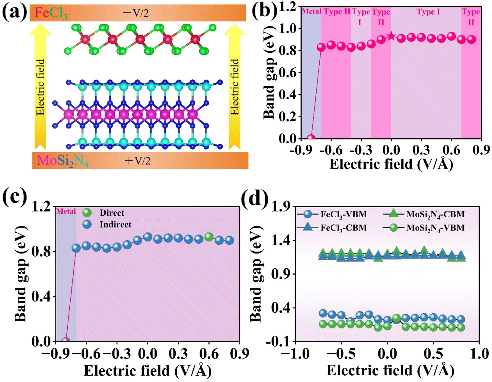 | ||
| Fig. 11 (a) Schematic of applying an electric field along the z direction of vdWH. (b) Band gap of FeCl3/MoSi2N4 vdWH as a function of electric field. (c) Band gap nature and (d) shifts in band-edge alignment under an electric field for FeCl3/MoSi2N4 vdWH. | ||
Fig. 11(b) shows the relationship between the band gap and the applied electric field. As the electric field strength is increased from −0.7 to 0.8 V Å−1, there is no significant change in the band gap, which fluctuates around 0.9 eV. This indicates that for the FeCl3/MoSi2N4 vdWH, the applied electric field does result in any noticeable changes in its band gap. However, when the electric field strength reaches −0.8 V Å−1, the band gap decreases sharply from 0.83 to 0 eV. The modulation of the band gap of the heterojunction and the semiconductor-to-metal transition under an applied vertical electric field can be explained as follows: when a co-directional positive electric field is applied, electron transfer from FeCl3 to MoSi2N4 is enhanced. However, minimal band gap modulation is observed due to charge transfer saturation and nonlinear band response. Conversely, under a reverse-biased negative field, the strong electric field reverses the net field direction, driving gradual electron transfer from MoSi2N4 to FeCl3. This progressive accumulation of reverse charges reconstructs interfacial band bending, leading to a gradual narrowing of the band gap. The electric field induces interfacial band bending by creating an electrostatic potential gradient between the FeCl3 and MoSi2N4 layers. This drives electron redistribution, shifting the Fermi level and altering band alignment. At a critical field strength (e.g., −0.8 V Å−1), the intensified band bending causes the CBM and VBM to overlap in momentum space, effectively closing the band gap, at which point the band gap drops to 0 eV, achieving the transition from a semiconductor to a metal. Simultaneously, charge transfer from low-work-function MoSi2N4 (5.16 eV) to high-work-function FeCl3 (6.23 eV) generates interfacial dipole moments, further amplifying band realignment. When the electric field exceeds the critical threshold, the Fermi level penetrates the conduction band, enabling unrestricted electron movement and metallic behavior. This electric-field-tunable electronic transition demonstrates the potential of the heterostructure for reconfigurable nanoelectronic devices.
Fig. 11(c) demonstrates the reversible indirect-to-direct band gap evolution in the heterostructure under an electric field. At an applied electric field strength of 0.6 V Å−1, the VBM and CBM of the heterostructure converge at an identical high-symmetry point within the Brillouin zone, resulting in a direct band gap configuration. Under the other investigated electric field strengths, the heterostructure maintains an indirect band gap nature.
To clarify the mechanism of the band gap tuning using electric fields, we investigated the variation of the band edges in the FeCl3/MoSi2N4 vdWH under different electric field strengths, as depicted in Fig. 11(d). Under positive electric fields, the VBM and CBM bands of both FeCl3 and MoSi2N4 maintain rigid alignment with negligible band gap variation, indicating cooperative stabilization with the built-in electric field. Conversely, under negative electric fields, solely the VBM of FeCl3 undergoes progressive energetic upshifting, while all other band edges (i.e., the CBM of FeCl3, and VBM/CBM of MoSi2N4) remain largely unchanged. This results in significant band gap narrowing, primarily driven by the elevation of valence band FeCl3. This phenomenon reveals the targeted modulation capability of negative fields on the valence band FeCl3.
Fig. 12(a) presents the DOS at E = −0.2 V Å−1. From the figure, it can be seen that the VBE is provided by the Mo 4d orbitals in the MoSi2N4 monolayer, while the Fe 3d orbitals in the FeCl3 monolayer contribute the CBE. Therefore, the FeCl3/MoSi2N4 vdWH exhibits a type-II band alignment. Fig. 12(b) shows the DOS at E = 0.2 V Å−1, in which both the VBM and CBM are provided by the Fe 3d orbitals in the FeCl3 monolayer, indicating that the FeCl3/MoSi2N4 vdWH has a type-I band alignment. Using a similar analytical method, it can be determined that the FeCl3/MoSi2N4 vdWH transitions from type-I to type-II heterojunctions at E = −0.7, −0.6, −0.5, −0.2, −0.1, 0.7 and 0.8 V Å−1.
 | ||
| Fig. 12 DOS of the FeCl3/MoSi2N4 vdWH when the strength of electric field is (a) −0.2 and (b) 0.2 V Å−1. | ||
4. Conclusion
This study employed first-principles calculations to investigate the changes in the electronic properties of the FeCl3/MoSi2N4 vdWH with modulation of the interlayer distance, in-plane strain, and external electric field. The calculated binding energy, phonon spectra, and molecular dynamics simulations collectively demonstrate robust structural stability. The results indicate that the equilibrium interlayer distance for the FeCl3/MoSi2N4 vdWH is 3.35 Å. The band gap of FeCl3/MoSi2N4 is 1.21/2.21 eV, as determined using PBE/HSE06 calculations, and both the CBM and VBM are provided by the FeCl3 monolayer, suggesting that it can be classified as a type-I heterojunction. In addition, the VBE is primarily sourced from the Fe 3d states, and the CBE mainly originates from the hybridization between the Fe 3d and Cl 3p orbitals. The work functions of the FeCl3 and MoSi2N4 monolayers are 6.23 eV and 5.16 eV, respectively, and the work function of the FeCl3/MoSi2N4 vdWH is 6.08 eV. The band gap of the FeCl3/MoSi2N4 vdWH can be altered by adjusting the interlayer distance, in-plane strain, and applied electric field. The results reveal that the FeCl3/MoSi2N4 vdWH not only transitions from a type-I to type-II heterojunction but also shifts from a semiconductor to a metal. As the interlayer distance changes, the band gap decreases. In particular, at ΔD = 1.5 Å, the band gap becomes zero, indicating a successful transition from semiconductor to metal. When ΔD = 2.65 Å and 5.0 Å, the heterojunction type shifts from type-I to type-II. Within the applied strain ranges from −4 to 4%, the band gap gradually decreases. At ε = −4%, the band gap is reduced to zero. At strains of −1% and 2%, the heterojunction converts from type-I to type-II. When the applied electric field is in the range of −0.7 to 0.8 V Å−1, the changes in the band gap are negligible, with the gap remaining around 0.9 eV. However, at E = −0.8 V Å−1, the band gap drops to zero, causing the FeCl3/MoSi2N4 vdWH to transform into a metal. Therefore, simple adjustment of the interlayer distance, application of strain, and the use of external electric fields can effectively control the band gap and band alignment type of FeCl3/MoSi2N4 vdWH. These characteristics suggest the tunability and excellent electronic properties of the FeCl3/MoSi2N4 vdWH, indicating its broad application prospects in photodetectors, wearable devices, flexible electronics and optoelectronic devices.Data availability
The datasets used and analysed during the current study are available from the corresponding author upon reasonable request.Author contributions
Xinrui Chen: original draft writing, data curation. Su Su: data curation, investigation. Xuewen Wang: data curation, methodology. Xuanyu Chen: data curation, investigation. Syed Awais Ahmad: writing, methodology, investigation. Lin Xu: supervision, data curation, investigation, writing. Weibin Zhang: supervision, data curation, investigation, writing.Conflicts of interest
The authors declare that they have no known competing financial interests or personal relationships that could have influenced the work reported in this paper.Acknowledgements
This research was supported by the National Natural Science Foundation of China (No. 52262042) and Yunnan Fundamental Research Projects (grant No. 202301AT070060). Spring City Plan: the High-level Talent Promotion and Training Project of Kunming (2022SCP005), Yunnan Revitalization Talent Support Program.References
- T. M. Su and X. W. Zhu, Advanced Photocatalytic Materials for Environmental and Energy Applications, Materials, 2023, 16, 7197, DOI:10.3390/ma16227197.
- M. Ramírez-Hernández, J. Cox, B. Thomas and T. Asefa, Nanomaterials for Removal of Phenolic Derivatives from Water Systems: Progress and Future Outlooks, Molecules, 2023, 28, 6568, DOI:10.3390/molecules28186568.
- K. S. Novoselov, A. K. Geim, S. V. Morozov, D. Jiang, Y. Zhang, S. V. Dubonos, I. V. Grigorieva and A. A. Firsov, Electric field effect in atomically thin carbon films, Science, 2004, 306, 666–669, DOI:10.1126/science.1102896.
- K. S. Novoselov, A. K. Geim, S. V. Morozov, D. Jiang, M. I. Katsnelson, I. V. Grigorieva, S. V. Dubonos and A. A. Firsov, Two-dimensional gas of massless Dirac fermions in graphene, Nature, 2005, 438, 197–200, DOI:10.1038/nature04233.
- D. B. Farmer, H.-Y. Chiu, Y.-M. Lin, K. A. Jenkins, F. Xia and P. Avouris, Utilization of a Buffered Dielectric to Achieve High Field-Effect Carrier Mobility in Graphene Transistors, Nano Lett., 2009, 9, 4474–4478, DOI:10.1021/nl902788u.
- P. Boggild, Research on scalable graphene faces a reproducibility gap, Nat. Commun., 2023, 14, 7495, DOI:10.1038/s41467-023-36891-5.
- M. M. Uddin, M. H. Kabir, M. A. Ali, M. M. Hossain, M. U. Khandaker, S. Mandal, A. Arifutzzaman and D. Jana, Graphene-like emerging 2D materials: recent progress, challenges and future outlook, RSC Adv., 2023, 13, 33336–33375, 10.1039/d3ra04456d.
- W. Zhang, Z. Zhang, S. Kwon, F. Zhang, B. Stephen, K. K. Kim, R. Jung, S. Kwon, K.-B. Chung and W. Yang, Photocatalytic improvement of Mn-adsorbed g-C3N4, Appl. Catal., B, 2017, 206, 271–281, DOI:10.1016/j.apcatb.2017.01.034.
- X. C. Ma, X. Wu, H. D. Wang and Y. C. Wang, A Janus MoSSe monolayer: a potential wide solar-spectrum water-splitting photocatalyst with a low carrier recombination rate, J. Mater. Chem. A, 2018, 6, 2295–2301, 10.1039/c7ta10015a.
- L. Xu, W. Q. Huang, L. L. Wang, Z. A. Tian, W. Y. Hu, Y. M. Ma, X. Wang, A. L. Pan and G. F. Huang, Insights into Enhanced Visible-Light Photocatalytic Hydrogen Evolution of g-C3N4 and Highly Reduced Graphene Oxide Composite: The Role of Oxygen, Chem. Mater., 2015, 27, 1612–1621, DOI:10.1021/cm504265w.
- M. D. Hernandez-Alonso, F. Fresno, S. Suarez and J. M. Coronado, Development of alternative photocatalysts to TiO2: Challenges and opportunities, Energy Environ. Sci., 2009, 2, 1231–1257, 10.1039/b907933e.
- S. Huang, D. Luo, B. Yang, G. Chen, X. Liu, Z. Mei and N. Zhang, Constructing highly active interface between layered Ni(OH)2 and porous Mo2N for efficient electrocatalytic oxygen evolution reaction, Int. J. Hydrogen Energy, 2023, 48, 22091–22100, DOI:10.1016/j.ijhydene.2023.03.121.
- K. Qi, C. Zhuang, M. Zhang, P. Gholami and A. Khataee, Sonochemical synthesis of photocatalysts and their applications, J. Mater. Sci. Technol., 2022, 123, 243–256, DOI:10.1016/j.jmst.2022.02.019.
- R. Marschall, Semiconductor Composites: Strategies for Enhancing Charge Carrier Separation to Improve Photocatalytic Activity, Adv. Funct. Mater., 2014, 24, 2421–2440, DOI:10.1002/adfm.201303214.
- Q. Cui, X. Gu, Y. Zhao, K. Qi and Y. Yan, S-scheme CuInS2/ZnS heterojunctions for the visible light-driven photocatalytic degradation of tetracycline antibiotic drugs, J. Taiwan Inst. Chem. Eng., 2023, 142, 104679, DOI:10.1016/j.jtice.2023.104679.
- J. Zhang, Y. Zhao, K. Qi and S.-y. Liu, CuInS2 quantum-dot-modified g-C3N4 S-scheme heterojunction photocatalyst for hydrogen production and tetracycline degradation, J. Mater. Sci. Technol., 2024, 172, 145–155, DOI:10.1016/j.jmst.2023.06.042.
- J. Lee and G. Kim, Electronic properties of a graphene/periodic porous graphene heterostructure, Carbon, 2017, 122, 281–286, DOI:10.1016/j.carbon.2017.06.049.
- K. Ren, K. Wang, Y. Cheng, W. Tang and G. Zhang, Two-dimensional heterostructures for photocatalytic water splitting: a review of recent progress, Nano Futures, 2020, 4, 032006, DOI:10.1088/2399-1984/abacab.
- W. Zhang, J. Guo, X. Lv and F. Zhang, Combined Machine Learning and High-Throughput Calculations Predict Heyd–Scuseria–Ernzerhof Band Gap of 2D Materials and Potential MoSi2N4 Heterostructures, J. Phys. Chem. Lett., 2024, 15, 5413–5419, DOI:10.1021/acs.jpclett.4c01013.
- A. Castro-Carranza, J. C. Nolasco, S. Bley, M. Rückmann, F. Meierhofer, L. Mädler, T. Voss and J. Gutowski, Effects of FeCl3 as Oxidizing Agent on the Conduction Mechanisms in Polypyrrole (PPy)/pc-ZnO Hybrid Heterojunctions Grown by Oxidative Chemical Vapor Deposition, J. Polym. Sci. Part B: Polym. Phys., 2016, 54, 1537–1544, DOI:10.1002/polb.24049.
- D. Zhan, J. X. Yan, Z. H. Ni, L. Sun, L. F. Lai, L. Liu, X. Y. Liu and Z. X. Shen, Bandgap-Opened Bilayer Graphene Approached by Asymmetrical Intercalation of Trilayer Graphene, Small, 2015, 11, 1177–1182, DOI:10.1002/smll.201402728.
- D. Zhan, L. Sun, Z. H. Ni, L. Liu, X. F. Fan, Y. Y. Wang, T. Yu, Y. M. Lam, W. Huang and Z. X. Shen, FeCl3-Based Few-Layer Graphene Intercalation Compounds: Single Linear Dispersion Electronic Band Structure and Strong Charge Transfer Doping, Adv. Funct. Mater., 2010, 20, 3504–3509, DOI:10.1002/adfm.201000641.
- X.-G. Hu, Q. Wei, Y.-M. Zhao, P.-X. Hou, W. Ren, C. Liu and H.-M. Cheng, FeCl3-functionalized graphene oxide/single-wall carbon nanotube/silicon heterojunction solar cells with an efficiency of 17.5%, J. Mater. Chem. A, 2022, 10, 4644–4652, 10.1039/d2ta00217e.
- A. Bafekry, M. Faraji, A. A. Ziabari, M. M. Fadlallah, C. V. Nguyen, M. Ghergherehchi and S. A. H. Feghhi, A van der Waals heterostructure of MoS2/MoSi2N4: a first-principles study, New J. Chem., 2021, 45, 8291–8296, 10.1039/d1nj00344e.
- J. Zeng, L. Xu, Y. Yang, X. Luo, H.-J. Li, S. X. Xiong and L.-L. Wang, Boosting the photocatalytic hydrogen evolution performance of monolayer C2N coupled with MoSi2N4: density-functional theory calculations, Phys. Chem. Chem. Phys., 2021, 23, 8318–8325, 10.1039/d1cp00364j.
- D. K. Pham, Electronic properties of a two-dimensional van der Waals MoGe2N4/MoSi2N4 heterobilayer: effect of the insertion of a graphene layer and interlayer coupling, RSC Adv., 2021, 11, 28659–28666, 10.1039/d1ra04531h.
- Q. Li, W. Zhou, X. Wan and J. Zhou, Strain effects on monolayer MoSi2N4: Ideal strength and failure mechanism, Phys. E, 2021, 131, 114753, DOI:10.1016/j.physe.2021.114753.
- G. K. Yang and Y. A. Zhou, MoSi2N4/WO2 van der Waals heterostructure: Theoretical prediction of an effective strategy to boost MoSi2N4′s nanoelectronic and optoelectronic applications, Comput. Mater. Sci., 2024, 231, 112617, DOI:10.1016/j.commatsci.2023.112617.
- X. Cai, Z. Zhang, Y. Zhu, L. Lin, W. Yu, Q. Wang, X. Yang, X. Jia and Y. Jia, A two-dimensional MoSe2/MoSi2N4 van der Waals heterostructure with high carrier mobility and diversified regulation of its electronic properties, J. Mater. Chem. C, 2021, 9, 10073–10083, 10.1039/d1tc01149a.
- J. Q. Ng, Q. Wu, L. K. Ang and Y. S. Ang, Tunable electronic properties and band alignments of MoSi2N4/GaN and MoSi2N4/ZnO van der Waals heterostructures, Appl. Phys. Lett., 2022, 120, 103101, DOI:10.1063/5.0083736.
- G. Kresse and J. Furthmüller, Efficiency of ab initio total energy calculations for metals and semiconductors using a plane-wave basis set, Comput. Mater. Sci., 1996, 6, 15–50, DOI:10.1016/0927-0256(96)00008-0.
- S. Grimme, Semiempirical GGA-type density functional constructed with a long-range dispersion correction, J. Comput. Chem., 2006, 27, 1787–1799, DOI:10.1002/jcc.20495.
- J. Heyd, G. E. Scuseria and M. Ernzerhof, Hybrid functionals based on a screened Coulomb potential, J. Chem. Phys., 2003, 118, 8207–8215, DOI:10.1063/1.1564060.
- C. Q. Nguyen, Y. S. Ang, S.-T. Nguyen, N. V. Hoang, N. M. Hung and C. V. Nguyen, Tunable type-II band alignment and electronic structure of C3N4/MoSi2N4 heterostructure: Interlayer coupling and electric field, Phys. Rev. B, 2022, 105, 045303, DOI:10.1103/PhysRevB.105.045303.
- Y.-L. Hong, Z. Liu, L. Wang, T. Zhou, W. Ma, C. Xu, S. Feng, L. Chen, M.-L. Chen, D.-M. Sun, X.-Q. Chen, H.-M. Cheng and W. Ren, Chemical vapor deposition of layered two-dimensional MoSi2N4 materials, Science, 2020, 369, 670, DOI:10.1126/science.abb7023.
- Y. Guo, L. Zhao and D. Zheng, Theoretical investigation on the electronic structure of new InSe/CrS2 van der Waals heterostructure, J. Mater. Res., 2022, 37, 2157–2164, DOI:10.1557/s43578-022-00548-8.
- M. K. Mohanta and A. De Sarkar, Interfacial hybridization of Janus MoSSe and BX (X = P, As) monolayers for ultrathin excitonic solar cells, nanopiezotronics and low-power memory devices, Nanoscale, 2020, 12, 22645–22657, 10.1039/d0nr07000a.
- D. Singh, N. Khossossi, A. Ainane and R. Ahuja, Modulation of 2D GaS/BTe vdW heterostructure as an efficient HER catalyst under external electric field influence, Catal. Today, 2021, 370, 14–25, DOI:10.1016/j.cattod.2020.09.025.
- M. Yankowitz, K. Watanabe, T. Taniguchi, P. San-Jose and B. J. LeRoy, Pressure-induced commensurate stacking of graphene on boron nitride, Nat. Commun., 2016, 7, 13168, DOI:10.1038/ncomms13168.
- Z. Dai, L. Bai, J. Wang and Z. Zhang, A first-principles study of Ti2B2T2/MoSi2N4 (T = F, O, OH) van der Waals heterostructures: Response characteristics to external electric field and uniaxial strain, Surf. Interfaces, 2024, 48, 104305, DOI:10.1016/j.surfin.2024.104305.
Footnote |
| † Electronic supplementary information (ESI) available. See DOI: https://doi.org/10.1039/d5ra02387d |
| This journal is © The Royal Society of Chemistry 2025 |