DOI:
10.1039/D5RA02254A
(Paper)
RSC Adv., 2025,
15, 14893-14902
Enhanced structural and optoelectronics performance of perovskite solar cells via MnSe2 incorporation in a MAPbI3 absorber layer
Received
1st April 2025
, Accepted 2nd May 2025
First published on 7th May 2025
Abstract
This study presents a novel approach for enhancing the efficiency of perovskite solar cells (PSCs) by incorporating MnSe2 into a MAPbI3 absorber layer. UV-visible (UV-vis) spectroscopy revealed a redshift in the absorption edge, reducing the bandgap from 1.71 eV to 1.62 eV, indicating improved light absorption. The refractive index increased from 2.84 to 2.89, while the extinction coefficient increased from 2.215 to 2.222, ensuring minimal non-radiative losses. Photoluminescence (PL) spectroscopy exhibited an enhanced emission peak, suggesting reduced non-radiative recombination. X-ray diffraction (XRD) analysis showed an increased crystallite size from 25.4 nm to 34.1 nm, with a decrease in dislocation line density (DLD) from 1.55 × 10¹⁵ to 0.86 × 10¹⁵, indicating improved crystallinity. Electrochemical impedance spectroscopy (EIS) revealed an increase in recombination resistance (Rrec) from 4835 Ω to 5941 Ω, confirming reduced charge recombination. Current density–voltage (J–V) measurements demonstrated an increase in power conversion efficiency (PCE) from 18.09% (MAPbI3) to 21.95% (MnSe2–MAPbI3), attributed to enhanced charge transport and energy band modification. External quantum efficiency (EQE) measurements further validated the improved light-harvesting capability of MnSe2–MAPbI3. These findings highlight MnSe2 as a promising additive for high-performance PSCs, offering improved optical, structural, and photovoltaic properties. Future research can explore stability enhancement for long-term device performance.
1. Introduction
The expanding energy problem, which is being brought on by the depletion of fossil fuel reserves and rising global energy use, has raised the need for sustainable and renewable energy sources.1 The quantity of solar energy and its benefits for the environment have made it a viable alternative.2 In particular, photovoltaic (PV) technology has made tremendous strides, and perovskite solar cells (PSCs) have shown remarkable potential due to their high efficiency and low production costs.3 The improved stability and environmental robustness of inorganic PSCs have made them attractive substitutes for organic and hybrid perovskites. For application in solar cells, a variety of inorganic perovskite compositions, such as CsPbI3, CsPbBr3, and CsSnI3, have been studied.4 Nonetheless, methylammonium lead iodide (MAPbI3) continues to be the most studied perovskite because of its remarkable optoelectronic characteristics, which include a long charge carrier diffusion length, a high absorption coefficient, and an adjustable bandgap (∼1.75 eV).5 PSCs based on MAPbI3 are comparable to traditional silicon-based solar cells due to their high power conversion efficiencies (PCEs).6 Despite these advantages, MAPbI3 vulnerability to moisture and heat instability causes stability issues under ambient conditions.7,8 To try to reduce these limitations, researchers have employed strategies including compositional engineering, surface passivation, doping, and encapsulation. MoSe2 was added to MAPbI3 perovskite by Ahmad et al., who claimed that this increased device stability by up to 85%.8 Maqsood et al. looked at how adding FA to MAPbI3 increased device stability and efficiency by up to 22.02%.9 Black phosphorous was added to MAPbI3, increasing the electron and hole charge carrier's diffusion lifespan, according to Liu et al.10 The focus of recent developments is on material advances to increase energy devices' stability and efficiency. Lattice engineering and multicomponent doping have produced high-entropy titanates with exceptional mechanical and thermal characteristics.11 Bi-interfacial modification techniques employing fluoropyridinic acid for better defect passivation in PSCs and controlled etching for silicon recycling, also demonstrate new avenues for producing long-lasting and high-performing solar cells.12,13
Among the various approaches to enhance the stability and efficiency of MAPbI3 PSCs, doping and additive strategies have emerged as effective methods. Doping elements like alkali metals, transition metals, and halides into the perovskite structure can improve charge transport properties and reduce trap states.14 Electron transport layers (ETLs) such as TiO2, SnO2, and ZnO have also been optimized to improve charge extraction and device stability.15 Furthermore, additive strategies incorporating materials like 2D perovskites, quantum dots, and metal chalcogenides have shown promise in enhancing the performance of MAPbI3 PSCs. These strategies address critical issues such as non-radiative recombination, defect passivation, and moisture resistance, leading to improved device efficiency and operational stability.16,17
Manganese selenide (MnSe2) has garnered interest because of its exceptional visual qualities, high carrier mobility, and distinct electrical structure.18 However, because of its comparatively worse stability and less-than-ideal band alignment for effective charge extraction, its independent use in photovoltaics has been restricted.18 Various researcher has studied the transition metals (Mn, Mo etc.) di-selenide-based materials for different application. The advantageous use of Cu-doped MnSe2 for the creation of hydrogen was documented by Soni et al.19 The Sm-doped MoSe2 ETL employed to improve the PCE for lead-based PSCs by Anandh et al.20 The potential of the MnSe2 electrode for use in supercapacitors was investigated by Phatak et al.21 Thus, the various researchers reported the MnSe2 application in the different field, but the performance of MnSe2 based material in the field of solar cell is still under investigation. MnSe2 can be added to MAPbI3 perovskite films to improve charge transport characteristics, passivate faults, and increase stability. The inherent drawbacks of MAPbI3 can be addressed by adding MnSe2, which can decrease trap states, inhibit non-radiative recombination, and increase carrier lifetime.22,23 Additionally, by partially replacing Pb with Mn, MnSe2–MAPbI3 composites can have a synergistic impact that improves the structural and optoelectronic characteristics of the perovskite layer while simultaneously lowering lead toxicity. This approach is in line with current research initiatives to create lead-free or lead-reduced PSCs with improved performance and environmental compatibility.22,23
This study introduces a novel approach to improving MAPbI3-based PSCs by incorporating MnSe2 as an additive. The key novelty of this work lies in the strategic incorporation of MnSe2 into MAPbI3 to enhance stability, and overall photovoltaic performance. The incorporation of MnSe2 into the perovskite structure is expected to improve crystallinity, reduce defect density, and enhance charge transport properties. The main findings of this study reveal that MnSe2–MAPbI3 films exhibit improved optoelectronic properties, leading to enhanced power conversion efficiency (PCE) from 18.09% to 21.95%. Additionally, the EIS and EQE analyses confirm reduced recombination losses and improved charge extraction in MnSe2-doped devices. This work contributes to the ongoing advancements in perovskite solar cell technology by presenting an effective strategy for enhancing the performance and stability of MAPbI3-based solar cells through MnSe2 incorporation.
2. Experimental details
2.1. Materials required
Sol–gel spin coating was used to create the MAPbI3 and 5% MnSe2–MAPbI3 films, and structural, optical, and electrical characterisations were then performed.24,25 High-purity materials were employed for the synthesis process, including lead iodide (PbI2, 99.99%, Sigma-Aldrich), methylammonium iodide (MAI, 99.5%, GreatCell Solar), and manganese selenide (MnSe2, 99.9%, Sigma-Aldrich). Solvents such as dimethyl sulfoxide (DMSO, ≥99.9%, Sigma-Aldrich), N,N-dimethylformamide (DMF, ≥99.8%, Sigma-Aldrich), and isopropanol (IPA, ≥99.9%, Sigma-Aldrich) were utilized for precursor solution preparation. Titanium dioxide (TiO2, 99.7%, Sigma-Aldrich) served as the electron transport layer (ETL), while Spiro-OMeTAD (99.8%, Sigma-Aldrich) was used as the hole transport layer (HTL). Every chemical was utilized without any additional purification.
2.2. Synthesis
In order to create MAPbI3 films, a 1 M solution of PbI2 (461 mg) and MAI (159 mg) was prepared in 1 mL of a DMF![[thin space (1/6-em)]](https://www.rsc.org/images/entities/char_2009.gif) :DMSO combination (4:1 v/v). The mixture was then stirred for an hour at 70 °C to produce a uniform yellow solution. MnSe2 nanoparticles, which were initially dispersed in DMF:DMSO and sonicated for 30 minutes before mixing with PbI2 and MAI, were used in place of 5 mol% of PbI2 for the 5% MnSe2–MAPbI3 films.8 The same conditions were then used to agitate the solution. To improve surface wettability, FTO-coated glass substrates were ultrasonically cleaned for 15 minutes each in acetone, ethanol, and isopropanol. This was followed by a 10-minute oxygen plasma treatment. A two-step spin coating procedure was used to deposit the films on FTO: 1000 rpm for 10 s was used to distribute the solution, and then 4000 rpm for 30 s was used. After 10 seconds, 300 μL of toluene was dropped to help crystallise the film. To finish the perovskite conversion, the films were then annealed for 15 minutes at 100 °C within a glove box (O2 < 0.1 ppm, H2O < 0.1 ppm).8
:DMSO combination (4:1 v/v). The mixture was then stirred for an hour at 70 °C to produce a uniform yellow solution. MnSe2 nanoparticles, which were initially dispersed in DMF:DMSO and sonicated for 30 minutes before mixing with PbI2 and MAI, were used in place of 5 mol% of PbI2 for the 5% MnSe2–MAPbI3 films.8 The same conditions were then used to agitate the solution. To improve surface wettability, FTO-coated glass substrates were ultrasonically cleaned for 15 minutes each in acetone, ethanol, and isopropanol. This was followed by a 10-minute oxygen plasma treatment. A two-step spin coating procedure was used to deposit the films on FTO: 1000 rpm for 10 s was used to distribute the solution, and then 4000 rpm for 30 s was used. After 10 seconds, 300 μL of toluene was dropped to help crystallise the film. To finish the perovskite conversion, the films were then annealed for 15 minutes at 100 °C within a glove box (O2 < 0.1 ppm, H2O < 0.1 ppm).8
2.3. Characterization
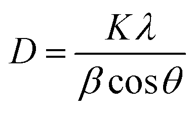
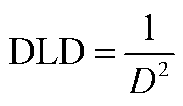
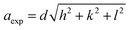
Tauc's relation was used to compute the optical bandgap (Eg), and Shimadzu UV-2600 UV-vis spectroscopy was used to analyze the films'optical properties:26where,  , for direct bandgap semiconductors, n = 2, d is the film thickness, α is the absorption coefficient, hv is the photon energy, and A is a constant. To assess charge carrier recombination, the photoluminescence (PL) spectra were recorded using a Horiba FluoroMax-4. The structural characteristics were analyzed using X-ray diffraction (XRD, PANalytical X'Pert Pro) with a Cu-Kα (λ = 1.5406 Å) source. Scherrer's eqn (2) was used to determine the crystallite size (D), while eqn (3) and (4) were used to determine the dislocation density (DLD), the lattice constant (a), and Bragg's law was used to estimate the interplanar spacing (d), as shown in eqn (5) below:27,28
| |
 | (2) |
| |
 | (3) |
| |
 | (4) |
| |
 | (5) |
where the Miller indices are (h, k, l), K is 0.9, θ is the X-ray wavelength, β is the full-width at half maximum (FWHM), and θ is the Bragg angle. The perovskite solar cell (PSC) devices were fabricated in the structure FTO/TiO2/MAPbI3/Spiro-OMeTAD/Au and FTO/TiO2/MnSe2–MAPbI3/Spiro-OMeTAD/Au to evaluate photovoltaic performance. A Keithley 2400 Source Meter was used to assess J–V characteristics in an AM 1.5G illumination setting (100 mW cm−2, Newport Solar Simulator). The fill factor (FF) and power conversion efficiency (PCE) were calculated using the following formulae:29| |
 | (6) |
| |
 | (7) |
where JSC is the short-circuit current density, VOC is the open-circuit voltage, FF is the fill factor, and Pin is the incident power. An Autolab PGSTAT302N was used for EIS between 1 Hz and 1 MHz in order to extract characteristics like recombination resistance (Rrec) and charge transfer resistance (Rct). A Newport Oriel IQE-200 was used to measure the EQE spectra in order to assess the wavelength-dependent photocurrent response.
3. Results and discussion
3.1. UV-vis spectroscopy
The UV-vis absorption spectra of 0%, 4%, 5%, and 6% MnSe2-incorporated MAPbI3 films are shown in Fig. 1a. All the prepared perovskite films show extensive absorption in the visible spectrum. Interestingly, the absorption edge changes when MnSe2 is added. The pure MAPbI3 film exhibits an excitonic absorption start at 725 nm. While 4%, and 5% MnSe2–MAPbI3 films display redshifts to 737 nm and 742 nm, followed by a minor blueshift to 723 nm for 6% MnSe2. Better orbital overlap and lower bandgap transitions are made possible by increased crystallinity and decreased defect density, which are the reasons for the redshift up to 5% MnSe2.30,31 Phase segregation, which provides localized states that impede efficient absorption, or excessive doping, which causes lattice distortion, might be the cause of the following blueshift at 6% MnSe2. In photovoltaic applications, redshifted absorption is especially advantageous since it makes it possible to gather lower-energy photons, so expanding the useable solar spectrum. The prolonged absorption of the 5% MnSe2–MAPbI3 film in this instance indicates improved photo-response, which makes it an excellent choice for an active layer in PSCs.31
 |
| | Fig. 1 (a) Absorption graph, (b) Tau'c plots of MAPbI3, 4%, 5%, and 6% MnSe2–MAPbI3. (c) Calculated values of n and K of MAPbI3 and 5% MnSe2–MAPbI3. | |
Tau'c plots were used to examine the optical bandgap (Eg) of the films.32 The calculated bandgaps for MnSe2–MAPbI3 films are 1.71 eV, 1.68 eV, 1.62 eV, and 1.75 eV for 0%, 4%, 5%, and 6% MnSe2, respectively, as seen in Fig. 1b. Improved crystallinity, band tailing from mild doping, and electrical structural modulation that narrows the bandgap are the reasons for the bandgap decrease with increasing MnSe2 concentration up to 5%.11–13 Nevertheless, bandgap widening is seen at 6% doping, which might be brought on by non-radiative recombination centers that interfere with the charge transport channels or by too much MnSe2 bringing structural disorder.33 PSCs benefit from a lowered bandgap at 5% MnSe2 (1.62 eV) since it closely resembles the optimal bandgap range for single-junction solar cells,34 enabling improved light absorption and an elevated short-circuit current density (JSC). Accordingly, the optical analysis shows that the most advantageous optical properties for photovoltaic performance are provided by 5% MnSe2 inclusion into MAPbI3. Our PSCs are made from pure MAPbI3 and 5% MnSe2–MAPbI3 films, which are great options for creating effective perovskite solar cells. Additionally, as illustrated in Fig. 1c, the extinction coefficient (K) and refractive index (n) were examined to evaluate the optical behavior of the films.35 The extinction coefficient rose from 2.215 to 2.222, and the refractive index of MAPbI3 was determined to be 2.84, slightly increasing to 2.89 for MnSe2–MAPbI3. This modest increase in refractive index points to improved light-trapping and optical confinement in the MnSe2–MAPbI3 film, which can enhance photon recycling in the active layer and boost efficiency.36 The extinction coefficient, which measures the material's capacity to absorb light, little changes, suggesting that the addition of MnSe2 does not result in a significant amount of non-radiative losses. PSC performance is improved by the combined effect of a greater refractive index and a regulated extinction coefficient, which guarantee ideal optical characteristics for effective light management.37
3.2. PL intensity
The absorption edge shown in the UV-vis spectra is consistent with emission peaks at 729 nm and 744 nm, respectively, in the photoluminescence (PL) spectra of MAPbI3 and 5% MnSe2–MAPbI3 films, as illustrated in Fig. 2. The MnSe2–MAPbI3 PL peak redshift indicates a decrease in the bandgap, which demonstrates that the incorporation of MnSe2 has changed the electrical structure.8 Defect states or band bending effects, which promote carrier relaxation to lower energy levels prior to radiative recombination, are responsible for this change.8 Furthermore, effective suppression of non-radiative recombination losses is suggested by the observed rise in PL emission intensity upon insertion of MnSe2. By interacting with undercoordinated ions, MnSe2 may be able to passivate surface traps and grain boundary defects, reducing recombination centers associated with defects.38 By encouraging radiative recombination processes, this passivation increases the device's overall efficiency and carrier lifetime. This result emphasizes how important MnSe2 is for improving the perovskite film's optoelectronic quality.8,38
 |
| | Fig. 2 PL intensity of MAPbI3 and 5% MnSe2–MAPbI3. | |
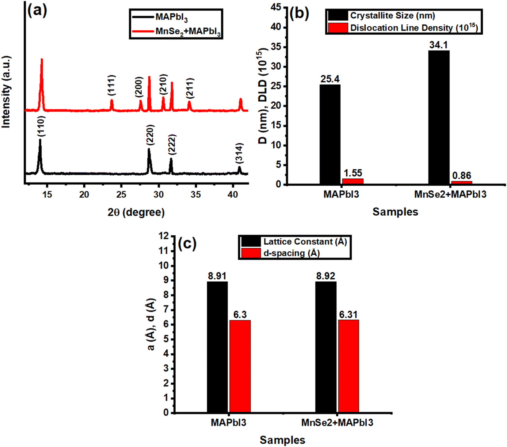
3.3. X-ray diffraction
An essential method for examining the crystalline quality, phase purity, and crystallographic structure of thin films is XRD. The XRD pattern of the MAPbI3 films displays distinctive diffraction peaks that correspond to the (110), (220), (222), and (314) crystal planes, as illustrated in Fig. 3a. These peaks are suggestive of the tetragonal phase of MAPbI3.8,39 A well-ordered crystal development within the film is confirmed by the crisp and well-defined diffraction peaks, which indicate good crystallinity. The successful production of the MAPbI3 phase with high purity is further guaranteed by the lack of secondary phases or peaks associated with impurities.40 By decreasing grain boundary defects, this high crystallinity significantly improves charge transport characteristics and raises the overall photovoltaic performance of perovskite solar cells (PSCs).41 Additional peaks at the (111), (200), (210), and (211) diffraction planes in the 5% MnSe2–MAPbI3 film's XRD pattern are ascribed to the presence of MnSe2 and are in good agreement with the JCPDS card number# 65-3336, confirming the successful incorporation of MnSe2 into the perovskite matrix.42 No secondary phases were detected in the XRD patterns after MnSe2 incorporation, confirming that MnSe2 is well integrated into the perovskite matrix without disrupting the MAPbI3 crystal structure. This supports the claim of enhanced crystallinity, as pure and sharp diffraction peaks indicate improved film quality.43–45 The MnSe2 addition functions as a nucleation site, enabling better grain formation, which is responsible for the observed increase in peak intensity in 5% MnSe2–MAPbI3 films when compared to pure MAPbI3.46 PSCs benefit from this increase in crystallinity because it lowers defect densities, increases charge carrier mobility, and decreases non-radiative recombination, all of which improve device performance.46 Using Scherrer's equation,27,28 the predicted crystallite size increases from 25.4 nm in pure MAPbI3 films to 34.1 nm in 5% MnSe2–MAPbI3 films, suggesting that MnSe2 addition improves grain growth. The improved crystalline quality of the MnSe2-based film is further supported by the dislocation line density (DLD), which is inversely correlated with crystallite size and drops from 1.55 × 10¹⁵ to 0.86 × 10¹⁵ lines per m2.47 Additionally, as seen in Fig. 3c, the structural characteristics for both films, including the lattice constant and d-spacing, were computed.27,28 From 8.91 Å in MAPbI3 to 8.92 Å in 5% MnSe2–MAPbI3, the lattice constant increases marginally, indicating a little lattice expansion brought on by MnSe2. In line with the change in peak positions, the d-spacing also rises from 6.30 Å to 6.31 Å.27,28 The slight expansion of the lattice parameter can be associated with strain relaxation effects introduced by MnSe2 incorporation, which aids in reducing defect states and improving film stability. This structural modification is advantageous for PSCs as it facilitates better charge transport, reduces defect-mediated recombination, and enhances light absorption, ultimately leading to improved power conversion efficiency.47
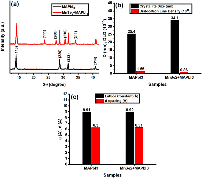 |
| | Fig. 3 (a) XRD patteren (b) calculated value of D and DLD (c) calculated values of a and d-spacing of MAPbI3 and 5% MnSe2–MAPbI3. | |
3.4. Device performance
As schematic diagram shown in Fig. 4a, two perovskite solar cell (PSC) devices were fabricated with the following configurations to examine the effect of the produced films as an active absorber layer such as device-1 (FTO\TiO2\MAPbI3\Spiro-OMeTAD\Au) and device-2 (FTO\TiO2\5%MnSe2–MAPbI3\Spiro-OMeTAD\Au). The absorption of photons by the perovskite active layer causes the creation of electron–hole pairs, in which holes migrate toward the hole transport layer (HTL) and electrons travel toward the electron transport layer (ETL).48 The ETL in the device construction is TiO2, which minimizes recombination losses by removing photogenerated electrons from the perovskite layer and transferring them toward the FTO electrode while obstructing hole transit.48 The light-absorbing substance that generates charge carriers is the perovskite layer (MAPbI3 or MnSe2–MAPbI3). In order to provide effective charge separation and transport within the device, the Spiro-OMeTAD serves as the HTL, gathering photogenerated holes from the perovskite layer and moving them in the direction of the Au electrode.48
 |
| | Fig. 4 (a) Schematic diagram of PSC (b) JV measurement (c) calculated values of JSC (mA cm−2) (d) calculated values of PCE (%) of device-1 (MAPbI3 based) and device-2 (MnSe2–MAPbI3 based) PSCs. | |
3.4.1. JV measurement. Fig. 4b shows the J–V characteristics of the two fabricated PSCs, demonstrating a notable improvement in performance for device-2 (5% MnSe2–MAPbI3-based). Table 1 presents the averaged photovoltaic parameters derived from J–V measurements of ten devices each for MAPbI3 and 5% MnSe2–MAPbI3, confirming the enhanced performance with MnSe2 incorporation. As summarized in Fig. 4(c) and (d), device-1 (MAPbI3-based) has a short-circuit current density (Jsc) of 19.61 mA cm−2, an open-circuit voltage (Voc) of 1.162 V, a fill factor (FF) of 0.794, and a power conversion efficiency (PCE) of 18.09%. The device-2 (5% MnSe2–MAPbI3), on the other hand, shows better values with Jsc = 23.43 mA cm−2, Voc = 1.168 V, FF = 0.802, and PCE = 21.95%. The addition of MnSe2, which efficiently alters the perovskite layer, lowering its energy bandgap and enhancing charge carrier dynamics, is responsible for the improvement in FF and PCE.49 Furthermore, improved electron injection into TiO2 is made possible by the conduction band alignment between TiO2 and MnSe2–MAPbI3, which lowers recombination losses. Because of the enhanced charge extraction and decreased recombination, device-2 (5% MnSe2–MAPbI3) performs better overall, making MnSe2–MAPbI3 a viable option for high-efficiency PSCs. Improvements in short-circuit current density (Jsc), fill factor (FF), and open-circuit voltage (Voc) are the main causes of the increase in PCE from 18.09% to 21.95%. Better charge carrier extraction and reduced recombination losses lead to enhanced Jsc and FF. Furthermore, reduced non-radiative recombination pathways are reflected in the elevated Voc.49,50
Table 1 Calculated photovoltaic parameters of 10, 10 devices-based on the perovskite (MAPbI3 and 5% MnSe–MAPbI3) from the JV measurement
| PSCs |
Voc (V) ±0.001 |
Jsc (mA cm−2) ±0.0043 |
FF ±0.002 |
Efficiency (%) ±0.004 |
| Pure MAPbI3 |
1.162 |
19.61 |
0.794 |
18.09 |
| 5% MnSe2–MAPbI3 |
1.168 |
23.43 |
0.802 |
21.95 |
3.4.2. EQE spectra. The External Quantum Efficiency (EQE) spectra of devices-1 (MAPbI3) and device-2 (5% MnSe2–MAPbI3) are shown in Fig. 5a. In line with the absorption profile of MAPbI3 perovskite materials, both devices show a robust photo response throughout a wide wavelength range of 300 nm to 800 nm. Interestingly, device-2 (5% MnSe2–MAPbI3) has a substantially greater EQE throughout the spectrum than device-1, especially in the 400–750 nm range. The addition of MnSe2, which improves interface quality and lowers charge recombination, is probably the cause of this improvement, which indicates better photon absorption and more effective charge carrier creation and extraction in device-2 (5% MnSe2–MAPbI3).9 Fig. 5b shows the integrated JSC values that correlate to the EQE spectra. According to the EQE curves trend, device-1 (MAPBI3) attains an integrated JSC of 17.82 mA cm−2, whereas device-2 gets a higher value of 22.97 mA cm−2. Better total photovoltaic performance is achieved by device-2 improved JSC, which represents its increased light-harvesting efficiency and greater charge collecting qualities. Importantly, the JSC values derived from EQE integration are marginally lower than the J–V curve measurements for both devices.10 The fact that EQE tests are usually carried out using a low-intensity monochromatic light source, which could not completely activate all photophysical processes within the device, provides a scientific reason for this disparity. High-intensity, broad-spectrum AM 1.5G illumination, on the other hand, is used for J–V measurements. In this setting, increased photon flux can result in greater trap state filling, light-induced defect passivation, and better carrier mobility, all of which can raise JSC values somewhat.9,10,51
 |
| | Fig. 5 (a and b) EQE spectra with corresponding Jsc of device-1 (MAPbI3 based) and device-2 (5% MnSe2–MAPbI3 based) PSCs. | |
3.4.3. EIS spectra. A potential method for examining charge transfer and recombination processes in PSCs is EIS. Recombination resistance (Rrec), or the device's resistance to charge carrier recombination, is one of the important characteristics taken from EIS.9 Better charge extraction and reduced recombination losses are indicated by a higher Rrec value, which enhances device performance. Device-1 and device-2 both have Nyquist plots in Fig. 6. The EIS measurements of PSCs were performed under dark conditions using a 10 mV AC perturbation around the maximum power point (MPP) bias voltage. EIS measurements were performed under dark conditions at the maximum power point (MPP) voltage to investigate intrinsic device impedance behavior.52 Under illumination, increased carrier generation could alter recombination dynamics and interface resistance, potentially leading to different impedance profiles.52 The frequency range was set from 1 MHz to 1 Hz. As shown in the inset of Fig. 6, a (R(CR)) equivalent Randles circuit model was used to fit the data with the help of ZSim software, in order to examine the EIS spectra.51 This circuit is consisting a component of a chemical capacitance (C), a recombination resistance (Rrec), and a series resistance (Rs) linked in series. Fig. 6 provides a summary of the fitted parameters. For both devices, the fitting value of Rs was found to be 18 Ω, demonstrating low wire and contact resistance.9 It was discovered that device-1 (MAPbI3) recombination resistance (Rrec–1) was 4835 Ω, but device-2 recombination resistance (Rrec–2) was 5941 Ω. Device-2 (5% MnSe2–MAPbI3) greater photovoltaic performance is compatible with a higher Rrec value, which indicates suppressed charge recombination. These findings suggest that device-2 superior charge transport characteristics and interface quality result in increased device stability and efficiency.51
 |
| | Fig. 6 EIS spectra of device-1 (MAPbI3 based) and device-2 (5% MnSe2-MAPbI3 based) PSCs with the inset (R(CR)) fitted circuit by ZSim software. | |
The operational stability of devices 1 and 2 during 250 hours under ambient settings is shown in Fig. 7. Device-1 (MAPbI3) barely kept 77.3% of its initial PCE, whereas device-2 (5% MnSe2–MAPbI3) kept 86.7%. The incorporation of MnSe2, which improves structural integrity and inhibits defect-induced degradation pathways, is responsible for device-2 (5% MnSe2–MAPbI3) better stability.53 Device-2 (5% MnSe2–MAPbI3) shorter PCE degradation suggests less ion migration and improved moisture resistance. Furthermore, MnSe2 passivation action may be reduces trap states, extending the device's lifespan. These results demonstrate that MnSe2 not only improves PSCs initial performance but also considerably extends their operating stability.53 Thus, incorporating MnSe2 into MAPbI3 offers two advantages over conventional additives: improved electrical interaction with TiO2 and efficient defect passivation. Better energy level alignment is made possible by MnSe2 layered structure, which speeds up electron transmission and lowers recombination losses. Improved device stability and photovoltaic performance are the outcomes of this synergistic interaction. MnSe2 is a very interesting addition for next-generation PSCs because of its multifunctionality.53
 |
| | Fig. 7 Stability test over 250 hours of device-1 (MAPbI3 based) and device-2 (5% MnSe2–MAPbI3) based PSCs. | |
4. Conclusions
This study demonstrates the enhancement of PSCs by incorporating MnSe2 into the MAPbI3 absorber layer. UV-vis spectroscopy revealed a redshift in the absorption edge, reducing the Eg from 1.71 eV to 1.62 eV, indicating improved light absorption. PL spectroscopy showed increased emission intensity, confirming reduced non-radiative recombination. XRD analysis indicated improved crystallinity, with an increased crystallite size from 25.4 nm to 34.1 nm and a decreased DLD. EIS analysis revealed increased Rrec, confirming suppressed charge recombination. J–V measurements demonstrated an increase in PCE from 18.09% to 21.95%, attributed to enhanced charge transport and bandgap modulation. EQE analysis confirmed improved photon harvesting. These findings establish 5% MnSe2–MAPbI3 as a promising candidate for high-performance PSCs with superior optical, structural, and photovoltaic properties. Although the incorporation of MnSe2 significantly improved device performance, a comprehensive defect density analysis and charge carrier mobility measurements are still needed. These studies could provide deeper insight into the intrinsic material properties and charge dynamics. Future work will focus on these aspects to further substantiate the current findings.
Data availability
The data supporting the findings of this study will be made available upon reasonable request from the corresponding author, Muhammad Saad (E-mail: msaad.comsats.edu@gmail.com).
Conflicts of interest
All the authors in this study, have no any type of conflict of interest.
Acknowledgements
The authors are thankful to the Deanship of Graduate Studies and Scientific Research at University of Bisha for supporting this work through the Fast-Track Research Support Program.
References
- T. Seyisi, et al., Major challenges for commercialization of perovskite solar cells: A critical review, Energy Rep., 2025, 13, 1400–1415 CrossRef.
- Z. Xingyu, Key Technologies for the Application of Perovskite Solar Cell Materials Under Energy Transition, in The Proceedings of 2024 International Conference of Electrical, Electronic and Networked Energy Systems: Volume VIII, Springer Nature, 2025 Search PubMed.
- L. Tariq, et al., Enlightening the hydrostatic pressure variation effect on physical properties of mechanically stable La2Ge2O7 pyrochlore oxide: Insights from first principles for solar cell advancement, Phys. B, 2025, 697, 416698 CrossRef CAS.
- R. Tsuji, et al., Hysteresis in Carbon-Based Multiporous Layered Electrode Perovskite Solar Cells with 5-AVA-MAPbI3 and CsFAPbI3, ACS Energy Lett., 2025, 10, 1275–1283 CrossRef.
- K. Zagorovskaia, et al., Improved Operational Lifetime of MAPbI3 Solar Cells Encapsulated with Parylene-N, Sol. RRL, 2025, 2400833 CrossRef CAS.
- J. V. Patil, S. S. Mali and C. K. Hong, Exceeding 23% Efficiency for 3D/3D Bilayer Perovskite Heterojunction MAPbI3/FAPbI3-Based Hybrid Perovskite Solar Cells with Enhanced Stability, Adv. Funct. Mater., 2025, 35(1), 2408721 CrossRef CAS.
- P. Tipparak, et al., The Impact of MAPbI3 Quantum Dots on CsFA Perovskite Solar Cells: Interface and Hole Extraction Improvement, ACS Appl. Energy Mater., 2025, 8(1), 355–365 CrossRef CAS.
- K. Ahmad, et al., Fabrication of lead halide perovskite solar cells with improved photovoltaic performance using MoSe2 additive strategies, Opt. Mater., 2024, 157, 116382 CrossRef CAS.
- A. Maqsood, et al., Perovskite solar cells based on compact, smooth FA 0.1 MA 0.9 PbI 3 film with efficiency exceeding 22%, Nanoscale Res. Lett., 2020, 15, 1–9 CrossRef.
- R. Liu, et al., Optimizing Black Phosphorus/Halide Perovskite Compositions by Scanning Photoelectrochemical Microscopy, J. Electrochem. Soc., 2022, 169(9), 096510 CrossRef CAS.
- C. Gao, et al., Novel high-entropy perovskite titanate: a potential thermal protective material with improved thermophysical properties, J. Eur. Ceram. Soc., 2025, 45(2), 116878 CrossRef CAS.
- K. Li, et al., Self-Induced Bi-interfacial Modification via Fluoropyridinic Acid For High-Performance Inverted Perovskite Solar Cells, Adv. Energy Mater., 2025, 15(11), 2404335 CrossRef CAS.
- F. Chen, et al., Short process recovery of silver and purification mechanism of crystalline silicon deep etching from end-of-life photovoltaic cells, Chem. Eng. J., 2025, 510, 161651 CrossRef CAS.
- Y. Yuan, et al., Enhanced Spontaneous Emission Rate and Luminescence Intensity of CsPbBr3 Quantum Dots Using a High-Q Microdisk Cavity, J. Phys. Chem. Lett., 2025, 16, 1095–1102 CrossRef CAS.
- S.-Y. Zhang, et al., Optimizing ETL/CsPbBr3 buried interface contact for enhanced efficiency and stability of inorganic perovskite solar cells, Rare Met., 2025, 1–11 Search PubMed.
- T. Wu, et al., Chlorine capped SnO2 quantum-dots modified TiO2 electron selective layer to enhance the performance of planar perovskite solar cells, Sci. Bull., 2019, 64(8), 547–552 CrossRef CAS.
- J.-B. Wu, C. Zhen and G. Liu, Photo-assisted Cl doping of SnO 2 electron transport layer for hysteresis-less perovskite solar cells with enhanced efficiency, Rare Met., 2022, 41, 361–367 CrossRef CAS.
- K. Yang, et al., Hollow nanocubes of MnSe2@ Cu3Se2/Cu2Se with heterostructure for ultrahigh-rate sodium storage, Chem. Eng. J., 2025, 160419 CrossRef CAS.
- A. Soni, Development of novel CuMnSe2/ppy hybrid structure for enhancing OER electrocatalytic activity in basic environment, J. Environ. Chem. Eng., 2025, 13(3), 116690 CrossRef.
- B. Anandh, et al., Enhanced photovoltaic performance of SmMoSe2 electron transport layer for perovskite solar cells, J. Mater. Sci.: Mater. Electron., 2025, 36(3), 1–20 CrossRef.
- M. Pathak, et al., A comparative experimental and theoretical investigation on energy storage performance of CoSe2, NiSe2 and MnSe2 nanostructures, Appl. Mater. Today, 2020, 19, 100568 CrossRef.
- M. Hussain, et al., Facile fabrication of FeSe/MnSe composite for improved electrochemical characterization by hydrothermal route, J. Electroanal. Chem., 2025, 976, 118787 CrossRef CAS.
- X. Liu, et al., Hydrothermal synthesis of cubic MnSe2 and octahedral α-MnSe microcrystals, J. Cryst. Growth, 2009, 311(5), 1359–1363 CrossRef CAS.
- M. Sadaqat, et al., Mn-based hierarchical polyhedral 2D/3D nanostructures MnX2 (X= S, Se, Te) derived from Mn-based metal–organic frameworks as high-performance electrocatalysts for the oxygen evolution reaction, Energy Fuels, 2022, 36(17), 10327–10338 CrossRef CAS.
- A. M. Babeer, Electronic and optoelectronic characteristics of Al/MnSe2/p-Si/Al diode, J. Mol. Struct., 2021, 1245, 131047 CrossRef CAS.
- P. R. Jubu, et al., Considerations about the determination of optical bandgap from diffuse reflectance spectroscopy using the Tauc plot, J. Opt., 2024, 1–11 Search PubMed.
- C. Humphreys, The significance of Bragg's law in electron diffraction and microscopy, and Bragg's second law, Found. Crystallogr., 2013, 69(1), 45–50 CrossRef CAS PubMed.
- A. Bokuniaeva and A. Vorokh, Estimation of particle size using the Debye equation and the Scherrer formula for polyphasic TiO2 powder, J. Phys. Conf. Ser., 2019, 1410(1), 012057 CrossRef CAS.
- J. Wang, et al., Charge accumulation induced S-shape J–V curves in bilayer heterojunction organic solar cells, Org. Electron., 2011, 12(6), 880–885 CrossRef CAS.
- M. Li, et al., An ultrafast optical sensor for simultaneous detection of NH3 temperature and concentration based on ultraviolet absorption spectral redshift combined with spectral reconstruction, Sens. Actuators, B, 2025, 422, 136631 CrossRef CAS.
- F. Mondaca, et al., Photoluminescence properties of SnO2 nanoparticles doped with group VI elements (Cr, Mo, W) synthesized by pulsed laser ablation in liquid, Phys. B, 2025, 696, 416625 CrossRef CAS.
- R. Anburaja and S. Kaleemulla, Structural, Magnetic, and Dielectric Properties of Bi1-xCoxFeO3 Nanoparticles for Photocatalytic Application, Braz. J. Phys., 2025, 55(2), 1–14 CrossRef.
- L.-Y. Chen, et al., A review: strategies for reducing the open-circuit voltage loss of wide-bandgap perovskite solar cells, Chem. Commun., 2025, 61, 1063–1086 RSC.
- R. K. Dharman, A. Mariappan and T. H. Oh, Engineering bandgap energy of MoO3 nanorod heterostructure using AgVO3 for efficient photocatalytic degradation of antibiotic pollutant, Environ. Res., 2025, 268, 120829 CrossRef CAS PubMed.
- V. Kumar and J. K. Singh, Model for calculating the refractive index of different materials, Indian J. Pure Appl. Phys., 2010, 48, 571–574 CAS.
- C. Fei Guo, et al., Metallic nanostructures for light trapping in energy-harvesting devices, Light: Sci. Appl., 2014, 3(4), e161 CrossRef.
- P. Cheng, et al., New nanophotonics approaches for enhancing the efficiency and stability of perovskite solar cells, Adv. Mater., 2024, 36(17), 2309459 CrossRef CAS PubMed.
- H. Cheng, et al., Understanding and minimizing non-radiative recombination losses in perovskite light-emitting diodes, J. Mater. Chem. C, 2022, 10(37), 13590–13610 RSC.
- R. Sojati, Solvent Annealing as a Post-treatment: towards Single Crystalline Epitaxial MAPbI3, University of Twente, 2023 Search PubMed.
- C.-H. Yeh, et al., Collective Motion of Methylammonium Cations Affects Phase Transition and Self-Trapped Exciton Emission in MAPbI3 Films, 2024 Search PubMed.
- A. F. Castro-Méndez, J. Hidalgo and J. P. Correa-Baena, The role of grain boundaries in perovskite solar cells, Adv. Energy Mater., 2019, 9(38), 1901489 CrossRef.
- S. Saranya, et al., Nickel-Manganese bimetallic Selenide as an electrode for supercapcitor applications, Sustain. Energy Technol. Assessments, 2023, 59, 103376 CrossRef.
- X. Guo, et al., Non-coordinating charge transfer enables ultrafast desolvation of hydrated zinc ions in the outer Helmholtz layer for stable aqueous Zn metal batteries, Natl. Sci. Rev., 2025, 12(4), nwaf070 CrossRef PubMed.
- Y. Hu, S. Zhao and L. Chen, Prediction of Ruddlesden–Popper antiperovskites K4OBr2 and K4OI2 for potential thermoelectric application, J. Phys. Chem. C, 2025, 129(9), 4656–4663 CrossRef CAS.
- R.-M. Hao, et al., Strong absorption of silica over full solar spectrum boosted by interfacial junctions and light–heat–storage of Mg (OH) 2–(CrOx–SiO2), Chem. Eng. J., 2024, 497, 154979 CrossRef CAS.
- D. Kaura and S. Bansalb, 2D Magnetic Systems Magnetic Properties, Fundamentals of Low Dimensional Magnets, 2022, pp. 73–89 Search PubMed.
- L. Fu, et al., Defect passivation strategies in perovskites for an enhanced photovoltaic performance, Energy Environ. Sci., 2020, 13(11), 4017–4056 RSC.
- N. Ahmadvand, E. Mohammadi-Manesh and F. Divakan, Investigating the effect and structural properties of Graphene and Borophene on lead-free perovskite: Introducing the Graphene/CsSnCl3/Borophene, Mater. Sci. Eng., B, 2025, 316, 118138 CrossRef CAS.
- X. Zheng, et al., Boron doping of multiwalled carbon nanotubes significantly enhances hole extraction in carbon-based perovskite solar cells, Nano Lett., 2017, 17(4), 2496–2505 CrossRef CAS PubMed.
- J. Kniepert, et al., Reliability of charge carrier recombination data determined
with charge extraction methods, J. Appl. Phys., 2019, 126(20), 205501 CrossRef.
- F. Gao, et al., Enhancing efficiency of MAPbI3 perovskite solar cells with carbon quantum dot implanted g-C3N4: Controllable crystallization and surface passivation, J. Alloys Compd., 2025, 1017, 179119 CrossRef CAS.
- I. Zarazua, et al., Surface recombination and collection efficiency in perovskite solar cells from impedance analysis, J. Phys. Chem. Lett., 2016, 7(24), 5105–5113 CrossRef CAS PubMed.
- E. Fabbretti, et al., Enhancing the stability of inverted perovskite solar cells through Cu 2 ZnSnS 4 nanoparticles hole transporting material, Sustain. Energy Fuels, 2025, 9, 1486–1497 RSC.
|
| This journal is © The Royal Society of Chemistry 2025 |
Click here to see how this site uses Cookies. View our privacy policy here. 
 Open Access Article
 This Open Access Article is licensed under a Creative Commons Attribution-Non Commercial 3.0 Unported Licence
 b,
Sadia Kanwala,
Muhammad Umar Farooqc,
Qurat Ul Aindf and
Muhammad Saad
b,
Sadia Kanwala,
Muhammad Umar Farooqc,
Qurat Ul Aindf and
Muhammad Saad , for direct bandgap semiconductors, n = 2, d is the film thickness, α is the absorption coefficient, hv is the photon energy, and A is a constant. To assess charge carrier recombination, the photoluminescence (PL) spectra were recorded using a Horiba FluoroMax-4. The structural characteristics were analyzed using X-ray diffraction (XRD, PANalytical X'Pert Pro) with a Cu-Kα (λ = 1.5406 Å) source. Scherrer's eqn (2) was used to determine the crystallite size (D), while eqn (3) and (4) were used to determine the dislocation density (DLD), the lattice constant (a), and Bragg's law was used to estimate the interplanar spacing (d), as shown in eqn (5) below:27,28