
 Open Access Article
 This Open Access Article is licensed under a Creative Commons Attribution-Non Commercial 3.0 Unported Licence
First-principles study of Ga2Ge2S3Se3 monolayer: a promising photocatalyst for water splitting†
Pham D. Trung *a and
Hien D. Tongb
*a and
Hien D. Tongb
aYersin University, 27 Ton That Tung, Ward 8, Dalat City, Lam Dong Province, Vietnam. E-mail: phdtrung2018@gmail.com
bFaculty of Engineering, Vietnamese-German University (VGU), Ben Cat City, Binh Duong Province, Vietnam
First published on 17th March 2025
Abstract
Recently, the quaternary Janus monolayers with the formula A2B2X3Y3 have been shown to be promising candidates for optoelectronic applications, especially in the photocatalytic water splitting reaction. Therefore, first-principles calculations were employed to investigate the photocatalytic properties of Ga2Ge2X3Y3 (X and Y represent S, Se or Te atoms) monolayers. The Ga2Ge2S3Se3 and Ga2Ge2Se3Te3 monolayers exhibit dynamic and thermal stability, supported by high cohesive energies (3.78–4.20 eV) and positive phonon dispersion. With a moderate Young's modulus (50.02–65.31 N m−1) and high Poisson's ratio (0.39–0.41), these monolayers offer a balance of stiffness and flexibility, making them suitable for flexible electronic applications. Especially, the difference in work function of 0.27 eV induces an intrinsic electric field in the Ga2Ge2S3Se3 monolayer, making the electronic structure of this material be suitable for the photocatalytic water splitting process. With light irradiation, the oxygen evolution reaction (OER) happened simultaneously, producing electrons and H+ protons for the hydrogen evolution reaction (HER) to happen at a low potential barrier. Moreover, the Ga2Ge2S3Se3 monolayer has a high absorption rate α(ω) of 105–106 cm−1 and a high electron mobility of 430.82–461.50 cm2 V−1 s−1. These characteristics result in a good solar-to-hydrogen  of the Ga2Ge2S3Se3 monolayer (14.80%) which is promising for use in photon-driven water splitting.
1 Introduction
Water splitting, the process of decomposing water into hydrogen and oxygen through electrolysis, offers a potential solution to the global energy crisis. This technology holds the promise of a clean, sustainable, and efficient energy future. A variety of materials have been explored as photocatalysts for water splitting, each with its unique properties and potential advantages. Inorganic semiconductors, such as metal oxides (TiO2, ZnO, Fe2O3),1–3 metal sulfides (CdS, ZnS),4,5 and metal nitrides (TiN),6 have been extensively studied. While these materials offer stability and high catalytic activity, their performance is often limited by factors like wide bandgaps and rapid charge carrier recombination. Organic semiconductors, including graphitic carbon nitride (g-C3N4) and organic dyes,7,8 offer advantages such as low cost and tunable bandgaps. However, their stability and efficiency can be compromised. Hybrid materials, combining the best of both inorganic and organic worlds, have emerged as promising candidates.9 These materials often exhibit enhanced light absorption, charge separation, and stability.To further enhance the efficiency of photocatalytic water splitting, researchers are exploring various strategies. Bandgap engineering, which involves modifying the bandgap of materials to better match the solar spectrum, is a key approach. Additionally, strategies to prevent electron–hole recombination, such as introducing co-catalysts or forming heterojunctions, are being investigated.3,10 Surface modification techniques are employed to improve light absorption and charge transfer, while nanostructuring is used to increase surface area and light harvesting efficiency.4,5 These advancements hold the potential to significantly improve the performance of photocatalytic water splitting systems.
Among 2D materials, ternary 2D chalcogenides have emerged as promising materials for photocatalytic water splitting due to their unique electronic and optical properties.11 Compounds like ZnIn2S4 and AgInS2 have garnered significant attention.12 These materials often exhibit suitable bandgap energies for visible light absorption, efficient charge carrier separation, and enhanced stability compared to their binary counterparts.13 However, challenges such as photocorrosion and low carrier mobility still need to be addressed. Ongoing research focuses on optimizing synthesis techniques, incorporating co-catalysts, and developing heterostructures to further improve the photocatalytic performance of these materials.
Two-dimensional (2D) layered transition metal phosphorus trichalcogenides (MPX3, where M represents transition metals and X = S, Se) exhibit high in-plane stiffness and lower cleavage energies than graphite.14–17 This allows them to be exfoliated down to atomic thickness. Recently, these materials have attracted renewed attention due to their unique structural and electronic properties. Notably, chemically exfoliated monolayer FePS3 has demonstrated efficient photocatalytic hydrogen evolution.18 Inspired by these findings, monolayers such as AsGeC3, SbSnC3, and BiPbC3 have been investigated, revealing strong stability and excellent optical properties.19 Additionally, CoGeSe3, GaSnS3, and InSnS3 monolayers show promise as visible-light photocatalysts with high carrier mobility.20,21 The GaGeSe3 monolayer, in particular, exhibits a solar-to-hydrogen conversion efficiency of 11.33% and a charge carrier mobility of 790.65 cm2 V−1 s−1.22 Substitution is an effective strategy for tuning the electronic properties of monolayers, as demonstrated experimentally. For instance, the MoSSe monolayer was synthesized by replacing the top-layer S atoms with Se atoms.23 Building on this concept, many quaternary monolayers have been theoretically designed based on the aforementioned ternary structures. The Zn2P2S3Se3 and Cd2P2S3Se3 monolayers are predicted to exhibit exceptionally high charge carrier mobility of 2772 cm2 V−1 s−1.24 Meanwhile, Janus-type monolayers such as In2Ge2Te3Se3, In2Ge2Se6, and In2Ge2S3Se3 have emerged as promising candidates for thermoelectric applications in high-temperature environments. In this study, the Ga2Ge2S3Se3 and Ga2Ge2Se3Te3 monolayers were constructed based on the atomic structures of GaGeS3 and GaGeSe3 monolayers, respectively. The structural, electronic and transport properties of the two new monolayers are studied using first-principles calculation.
2 Methodology
All calculations were performed using the Quantum-ESPRESSO package.25 The Perdew–Burke–Ernzerhof (PBE) functional26 within the generalized gradient approximation (GGA) and the hybrid functional HSE06 (ref. 27) were employed to describe exchange–correlation effects. Projector augmented-wave (PAW) pseudopotentials28 were used to represent core-valence electron interactions. An energy cutoff of 520 eV was chosen for effective convergence of the total energies. In addition, a density cutoff, four times the energy cutoff, was used in the calculations. The geometry was fully relaxed until the forces on all of the atoms decreased to less than 0.01 eV Å−1 and the total energy change was smaller than 10−6 eV. A 15 × 15 × 1 Monkhorst–Pack k-point mesh was used to sample the Brillouin zone. The initial structural models of Ga2Ge2S3Se3 and Ga2Ge2Se3Te3 monolayers were constructed based on the known structures of GaGeS3 and GaGeSe3, respectively. The 20 Å vacuum layers were added to avoid interactions between periodic images. The structural asymmetry of Ga2Ge2X3Y3 monolayers induces significant dipole moments, leading to notable van der Waals (vdW) interactions. To accurately account for these vdW interactions, DFT-D3 corrections29 were incorporated into the DFT functionals. The dynamic stability of the monolayers was assessed by calculating phonon dispersion curves using the functional perturbation method implemented in the PHONOPY code.30 Transport properties, including carrier mobility, were estimated using the deformation potential method.313 Results and discussion
3.1 Structural characteristics
The equilibrium configurations of Ga2Ge2X3Y3, shown in Fig. 1, were achieved by optimizing their lattice structures for the lowest energy. The top view of Ga2Ge2X3Y3, as shown in Fig. 1(a), has a hexagonal pattern constructed based on the rhombus unit-cell, which contains 10 constituent atoms including two Ga (green balls), two Ge (purple balls), three S/Se (red balls), and three Se/Te (brown) atoms. As illustrated in Fig. 1(b), these atoms are arranged in five sublayers of S/Se, Ge, Ga, Ge, and Se/Te atoms that are stacked on top of one another. On the right-hand side, Fig. 1(c) shows the dynamic characteristics of these structures in form of phonon dispersions. While Ga2Ge2S3Se3 and Ga2Ge2Se3Te3 monolayers are dynamically stable with positive phonons, the Ga2Ge2S3Te3 monolayer is predicted to be unstable due to the negative frequencies of some acoustic phonons. | ||
| Fig. 1 Optimized atomic structure of Ga2Ge2X3Y3 (X/Y = S, Se, Te; X ≠ Y) monolayers shown in (a) top view and (b) site view together with (c) their phonon dispersions. | ||
It is worth noting that the Ga2Ge2S3Se3 and Ga2Ge2Se3Te3 monolayers are formed by modifying the atomic structures of GaGeS3 and GaGeSe3 monolayers,22 respectively, where heavier atoms Se/Te are substituted for lighter host atoms S/Se. Such substitutions cause lattice enlargement, as shown in Table 1, the lattice constants (a = b) of Ga2Ge2S3Se3 and Ga2Ge2Se3Te3 monolayers are 6.29 Å and 6.74 Å, respectively. These lattice constants are about 0.17–0.28 Å longer than the corresponding values of GaGeS3 or GaGeSe3 monolayer.22 Due to the stacking of sublayer of identical elements, the substitution of Se atoms for S atoms replaces the whole S-sublayer in the GaGeS3 monolayer22 (S–Ge–Ga–Ge–S) with the Se-sublayer in the Ga2Ge2S3Se3 monolayer (S–Ge–Ga–Ge–Se). Such a significant change causes noticeable enlargement of all bond-lengths as GaGeS3 monolayer22 transforms into Ga2Ge2S3Se3 monolayer. As shown in Table 1, the Ge–S, Ga–S, and Ge–Ge bond lengths increase by 0.3–0.13 Å. Consequently, the monolayer thickness, which is defined as the distance between the two edge sublayers, also increases by about 0.08 Å. Similarly, the data listed in Table 1 shows that the replacement of Se-sublayer in GaGeSe3 monolayer22 with the Te-sublayer in Ga2Ge2Se3Te3 monolayer results in some increase in the Ge–Se, Ga–Se, and Ge–Ge bond lengths by about 0.04–0.22 Å. Meanwhile, the thickness of Ga2Ge2Se3Te3 monolayer is 0.12 eV.
| a (Å) | h (Å) | dGe–X (Å) | dGa–X (Å) | dGe–Ge (Å) | dGe–Y (Å) | dGa–Y (Å) | Ecoh (eV per atom) | EPBEg (eV) | EHSE06g (eV) | C11 (N m−1) | C12 (N m−1) | C66 (N m−1) | Y2D (N m−1) | ν2D | |
|---|---|---|---|---|---|---|---|---|---|---|---|---|---|---|---|
| Ga2Ge2S3Se3 | 6.29 | 3.28 | 2.37 | 2.66 | 2.37 | 4.20 | 1.02 | 1.83 | 76.69 | 29.55 | 23.57 | 65.31 | 0.39 | ||
| Ga2Ge2Se3Te3 | 6.74 | 3.50 | 2.42 | 2.57 | 2.87 | 3.78 | 0.06 | 0.63 | 59.82 | 24.21 | 17.81 | 50.02 | 0.41 |
The significant change in the structural characteristics of the two new monolayers requires further study on their stability. From an energy perspective, a new system is considered stable if its total energy is less than the combined energies of its individual components. Such energetic difference is called cohesive energy Ecoh, which can be calculated for the Ga2Ge2X3Y3 monolayers as follows:
 | (1) |
 | ||
| Fig. 2 (a and b) Total energy variation of Ga2Ge2S3Se3 and Ga2Ge2Se3Te3 monolayers at 300 K and 500 K; angular functions of (c) Young's modulus and (d) Poisson's ratio of Ga2Ge2S3Se3 (pink circles) and Ga2Ge2Se3Te3 (green circles) monolayers. | ||
The mechanical stability, stiffness and deformation behavior of 2D materials, such as graphene, transition metal dichalcogenides, and MXenes, etc.,33–35 can be analyzed using Born's stability criteria, Young's modulus (Y) and Poisson's ratio (ν), respectively. These properties are determined from the elastic constants C11, C12, and C66, which are derived by calculating the second partial derivatives of the total energy of the system with respect to the corresponding components of strain, thereby linking the material's atomic-level interactions to its macroscopic mechanical properties.36
For 2D hexagonal materials such Ga2Ge2S3Se3 and Ga2Ge2Se3Te3 monolayers, the Born's mechanical stability criteria are simplified due to their symmetry and two-dimensional nature as follows: C11 > 0, C66 > 0, and C11 − C12 > 0.37,38 As reported in Table 1, the calculated C11, C12 and C66 moduli of Ga2Ge2S3Se3 and Ga2Ge2Se3Te3 monolayers comply these criteria. These findings are crucial, as the Born criteria ensure the strength of materials under small deformations and indicate the absence of lattice instabilities. Furthermore, the Young's modulus and Poisson's ratio as angular functions were calculated in the xy plane. As plotted in Fig. 2(c) and (d) for Ga2Ge2S3Se3 and Ga2Ge2Se3Te3 monolayers, respectively, the graphs of these functions are nearly perfect circles. This angular dependence directly correlates with the structural isotropy and uniformity of these monolayers, underscoring their potential for applications where uniform mechanical properties are essential.39,40 The calculated Young's modulus values are 65.31 N m−1 for Ga2Ge2S3Se3 and 50.02 N m−1 for Ga2Ge2Se3Te3, placing them among 2D materials with moderate stiffness such as GaGeSe3, GaGeS3, Al2Ge2S3Se3, Al2Ge2Se3Te3, tinselenidene and bismuth telluride nanosheets.22,32,41,42 Meanwhile, Ga2Ge2S3Se3 and Ga2Ge2Se3Te3 monolayers are more flexible than phosphorene, graphene, black phosphorus (BP), hexagonal boron nitride and MoS2 monolayer.43–45 The reduced modulus compared to graphene can be attributed to the buckled structure and the chemical composition of these monolayers, which result in lower in-plane bonding strength. This intermediate stiffness makes Ga2Ge2S3Se3 and Ga2Ge2Se3Te3 suitable for applications requiring flexibility without significant loss of mechanical stability. In addition, the Poisson's ratios of Ga2Ge2S3Se3 and Ga2Ge2Se3Te3 range from 0.39 to 0.41, exceeding those observed in many ternary and quaternary monolayers of similar atomic structures, including GaGeS3, GaGeSe3, and Al2Ge2Se3Te3.22,32 A high Poisson's ratio indicates the material's ability to undergo lateral expansion when stretched, which is a desirable trait for enhancing toughness and ductility. For comparison, the Poisson's ratios of typical 2D transition metal dichalcogenides MoS2 and WS2, tin chalcogenides, boron nitride (h-BN)46–48 hover around 0.3, making Ga2Ge2S3Se3 and Ga2Ge2Se3Te3 superior in terms of toughness and deformation resilience.
This combination of moderate stiffness and high Poisson's ratio suggests that Ga2Ge2S3Se3 and Ga2Ge2Se3Te3 monolayers can endure significant deformation without losing their structural integrity. The demonstration of FeClF, MnSeTe, and MnSTe monolayers as promising materials for a wide range of electronic applications, particularly due to their favorable elastic properties,49,50 provides strong support for considering Ga2Ge2S3Se3 and Ga2Ge2Se3Te3 as potential candidates for flexible electronic devices, such as foldable displays, wearable sensors, and stretchable photovoltaics, where both mechanical resilience and flexibility are required.51–53 Furthermore, their structural and mechanical characteristics could enable their integration into composite materials to enhance performance under mechanical stress.
3.2 Electronic characteristics of Ga2Ge2S3Se3 and Ga2Ge2Se3Te3 monolayers
Fig. 3 presents the band structures of Ga2Ge2S3Se3 and Ga2Ge2Se3Te3 monolayers, calculated using both HSE06 (solid pink curves) and GGA-PBE (dashed blue curves) functionals. Both monolayers exhibit analogous band structure patterns, characterized by a high density of electronic states due to the large number of atoms in their unit cells. Notably, both materials possess direct band gaps, with the valence band maximum (VBM) and conduction band minimum (CBM) situated at the Γ – point. The HSE06 method offers a more accurate treatment of the exchange–correlation interaction, effectively suppressing the unphysical overestimation of electron energies in the valence bands. As a result, the calculated band gap between the valence and conduction bands is significantly larger in the HSE06 approach compared to the values calculated by the GGA-PBE method. For the Ga2Ge2S3Se3 monolayer, the HSE06 calculation yields a band gap of 1.83 eV, which is 0.81 eV larger than the value calculated by the GGA-PBE method. In the case of the Ga2Ge2Se3Te3 monolayer, the GGA-PBE method predicts an extremely narrow band gap of 0.06 eV. However, the HSE06 approach provides a significantly improved result, revealing a band gap of 0.63 eV.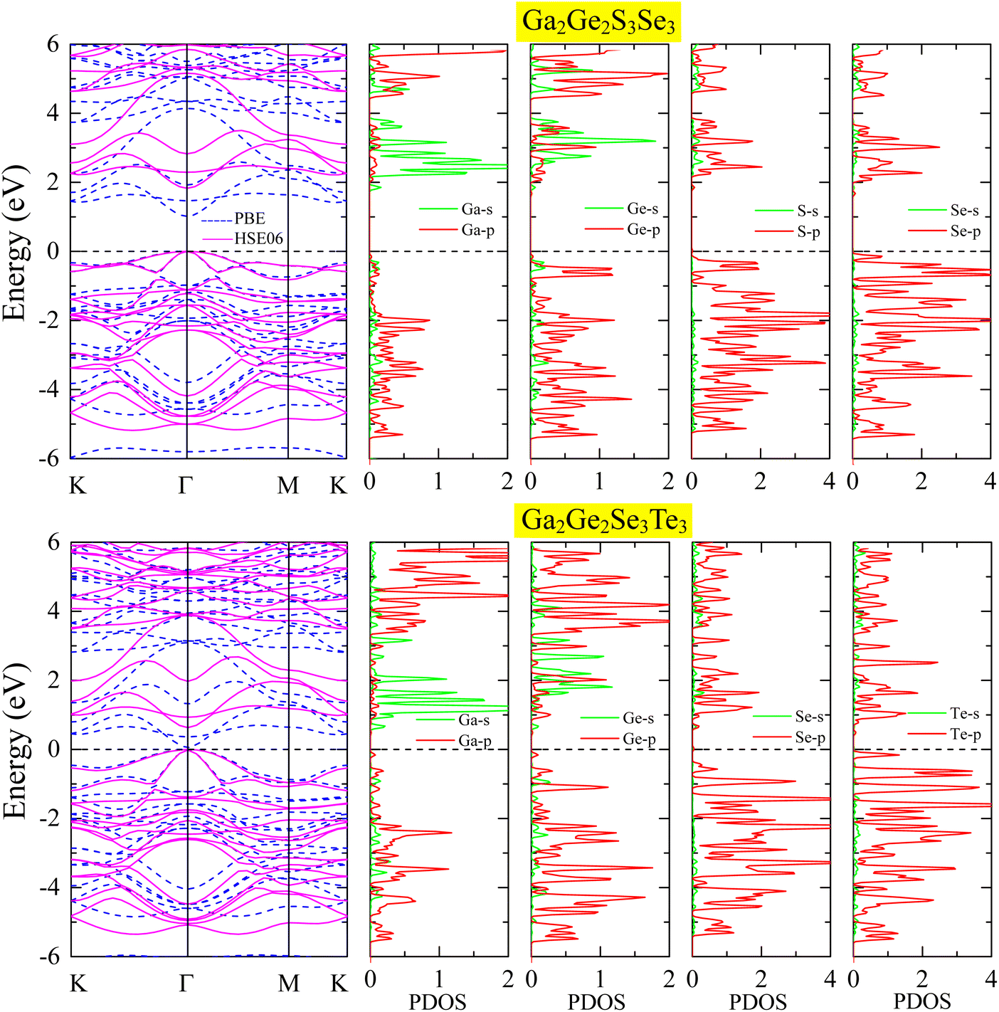 | ||
| Fig. 3 Electronic band structures and projected density of states (PDOS) ofGa2Ge2S3Se3 and Ga2Ge2Se3Te3 monolayers. The band structures were calculated using PBE functional (dash blue lines) and HSE06 hybrid functional (solid pink lines). | ||
Compared to the HSE06 band gaps of GaGeS3 (2.51 eV) and GaGeSe3 (1.91 eV) monolayers,22 replacing the S sublayer with a Se sublayer or the Se sublayer with a Te sublayer reduces the band gaps of the original monolayers. These results highlight that substituting heavier element provides an efficient strategy for narrowing the band gaps of monolayers. This effect results from the increased spin–orbit coupling (SOC) induced by heavier atoms, which brings the conduction and valence band edges closer together.54,55 In two-dimensional materials, the impact of SOC is further amplified by quantum confinement,56,57 leading to more pronounced band gap reductions and tunable electronic properties. The band gap of Ga2Ge2Se3Te3 is below 1.23 eV, rendering it unsuitable as a photocatalyst for water splitting due to insufficient energy for driving the reaction.58 In contrast, the Ga2Ge2S3Se3 monolayer is well-suited for this application. Additionally, it represents an advancement over the GaGeS3 monolayer,22 as its narrower band gap enables greater absorption of visible light, which makes up a significant portion of the solar energy spectrum. In the Ga2Ge2S3Se3 monolayer, the PDOS reveals that p-orbitals from Ga, Ge, S, and Se dominate both the valence and conduction bands across a wide energy range. Strong hybridization is observed, particularly between the s- and p-orbitals of Ga and Ge. The direct bandgap is formed by the valence band maximum (VBM) dominated by Se-p orbitals and the conduction band minimum (CBM) dominated by Ga-s orbitals. A similar PDOS profile is observed in the Ga2Ge2Se3Te3 monolayer, with p-orbitals from the constituent atoms dominating at all energy levels. The VBM is primarily composed of Te-p orbitals, while the CBM is dominated by Se-s, p orbitals and p-orbitals from the other atoms.
To gain deeper insights into the orbital contributions of each constituent element to the electronic band structure, we analyzed the projected band structures of Ga2Ge2S3Se3 and Ga2Ge2Se3Te3 monolayers, as depicted in Fig. 4. In these plots, the s, px, py, and pz orbitals are depicted in blue, pink, red, and green, and their relative contributions are visualized by the size of the corresponding spheres. By examining these projected band structures, we can identify the specific orbitals of each element that dominate the formation of the valence band maximum and conduction band minimum, providing valuable information about the electronic and hole transport properties of these materials. It is obvious that the highest valence bands are mainly occupied by Se-p orbitals in Ga2Ge2S3Se3 monolayer and by Te-p orbitals in Ga2Ge2Se3Te3 monolayer. Consequently, the width of the band gap is partially determined by the substituted Se or Te element. It is worth noting that the lowest conduction bands, on the other hand, are mainly constructed by the Ga-s orbitals, making them another important factor in creating the band gap.
 | ||
| Fig. 4 Orbital-projected band structures of Ga2Ge2S3Se3 and Ga2Ge2Se3Te3 monolayers. | ||
In Al2Ge2S3Se3 and Al2Ge2Se3Te3 monolayers, the bandgaps range from 1.07 to 2.38 eV.32 These values are smaller than those observed in Ga2Ge2S3Se3 and Ga2Ge2Se3Te3 monolayers. This reduction in bandgap can be attributed to the lighter atomic mass of Al compared to Ga, resulting in weaker SOC effects in the Al-containing compounds. When analyzing the bandgaps of In2Ge2S3Se3, In2Ge2S3Te3, Al2Ge2S3Se3, and Al2Ge2Se3Te3 monolayers32,59 within the A2B2X3Y3 family, it is observed that the Y atoms (Se or Te) play a significant role in determining the bandgap width. Specifically, heavier Y atoms result in narrower bandgaps. These findings confirm the mechanism discussed in the previous section, which emphasizes the significant influence of SOC on bandgap values. At lower valence bands, ranging from −2 to −1 eV, orbital hybridization is observed to happen between pz orbitals from Ge, S, and Se elements in Ga2Ge2S3Se3 monolayer or Ge, Se, and Te elements in Ga2Ge2Se3Te3 monolayer. The hybridization of other orbitals happens in the deeper energy levels. Meanwhile, the py orbitals from Se or Te atoms participate in the hybridization with other orbitals at almost all valence energy bands, showing the important role of Se and Te elements in the formation of covalent bonds in Al2Ge2S3Se3 and Al2Ge2Se3Te3 monolayers.
3.3 Photocatalytic performance of Ga2Ge2S3Se3 monolayer
Fig. 5(a) illustrates the variation in electrostatic potential across both sides of the Ga2Ge2S3Se3 monolayer. To move an elementary charge away from the monolayer's surface, work must be done against the electrostatic potential. The horizontal blue line in the diagram represents the vacuum level, where a free electron is no longer influenced by the material's potential. The work function (Φ) is defined as the energy required to move an electron from the Fermi level to the vacuum level. Due to the higher electronegativity of S compared to Se, the S-side of the monolayer exhibits a higher electrostatic potential. This results in a difference in work function (ΔΦ) of 0.27 eV between the two sides of the monolayer. As a result, an internal electric field E is induced,60 pointing from the lower-potential Se-side to the higher-potential S-side. This field facilitates the movement of photoexcited electrons from the S-side to the Se-side, while photoexcited holes move in the opposite direction. This promotes effective electron–hole separation, which not only enhances the material's photocatalytic efficiency but also influences the band edge alignment relative to the redox potential.60 The energies of the conduction band edge ECBE and valence band edge EVBE can be defined by formula proposed by Toroker et al.61,62 based on the energy at vacuum level EV and the energies of the unshifted conduction band minimum ECBM and valence band maximum EVBM as ECBE/VBE = ECBM − ES/Se-sideV. In Fig. 5(a), the positions of EVBE and ECBE are denoted with green and red solid rectangles, respectively. It is obvious that the EVBE is located below the oxidation potential O2/H2O and the ECBE is above the H+/H2 reduction potential. Therefore, it is expected that the Ga2Ge2S3Se3 monolayer can induce the separation of water to release oxygen and hydrogen gases if the energetic requirements are met. In Fig. 5(a), the positions of EVBE and ECBE are denoted by green and red solid rectangles, respectively. The diagram shows that the EVBE is positioned below the oxidation potential of water (O2/H2O), while the ECBE lies above the reduction potential of protons (H+/H2). This band alignment is typical for water splitting photocatalyst.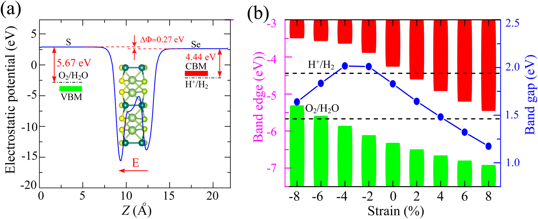 | ||
| Fig. 5 (a) Electrostatic potential with intrinsic electric field (red arrow) of Ga2Ge2S3Se3 monolayer and (b) the variation of bandgap and band edge alignment relative to the redox potential of water splitting reaction. | ||
Strain engineering emerges as a powerful tool for enhancing the photocatalytic activity of two-dimensional materials, particularly Janus structures like Ga2Ge2S3Se3. By applying strain, precise control over the bandgap and band alignment becomes possible. This allows for optimization of light absorption and efficient charge carrier transport, crucial for driving photocatalytic reactions.63–66 Furthermore, strain can effectively align the band edges with the redox potentials of water splitting reactions. This alignment facilitates efficient charge transfer and improves the overall catalytic efficiency.67,68 Most of 2D materials can withstand substantial strains, typically up to around 10%,69 before significant deformation or failure. This high flexibility stems from their unique atomic structure. However, it's crucial to recognize that this value is not universal and depends strongly on the specific material and the nature of the applied strain. For example, reported strain limits for 2D GeP range from 12.9% to 26.2%,70 and MoS2 monolayers have been shown to maintain stability above 10% strain.71 The Ga2Ge2S3Se3 and Ga2Ge2Se3Te3 monolayers, with their moderate Young's moduli (50.02–65.31 N m−1) and high Poisson's ratios (0.39–0.41), are predicted to be relatively flexible. Therefore, the compressive and tensile strains ranging from −8% to 8% were applied on these two monolayers. Our investigation delves into the impact of strain on the bandgap and band edge alignment of the Ga2Ge2S3Se3 monolayer (Fig. 5(b)). Compressive strains ranging from −2% to −4% lead to a bandgap widening of approximately 2.0 eV. Beyond this range, both further compression and tensile strains result in a bandgap reduction. Notably, the band edges of the Ga2Ge2S3Se3 monolayer remain suitable for water redox reactions when subjected to compressive strains between −6% and −8% or tensile strains below 4%.
Strain engineering offers a versatile approach to fine-tune the electronic and optical properties of 2D materials, including their bandgap, band edge positions, and light absorption characteristics. These tunable properties hold significant potential for enhancing photocatalytic performance in applications such as water splitting.72–74 Given the promising photocatalytic potential of Ga2Ge2S3Se3 monolayer, we investigated the effects of strain ranging from −8% to 8%. The resulting changes in band structure and light absorption rate are illustrated in Fig. 6, respectively.
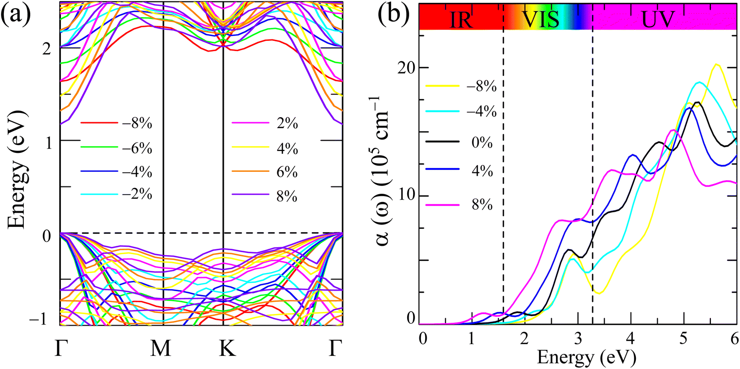 | ||
| Fig. 6 (a) Impact of strain on the band structure and (b) the light absorption rate of the Ga2Ge2S3Se3 monolayer. | ||
Fig. 6(a) presents the band structures with the valence band maximum (VBM) aligned to the Fermi level, allowing us to focus on the shifts in the conduction band minimum (CBM). Previous studies on black phosphorus, transition metal dichalcogenides, and ternary Janus monolayers have demonstrated that strain can induce significant band structure modifications, such as direct-to-indirect bandgap transitions, bandgap tuning, and changes in band curvature.75,76 In contrast, the Ga2Ge2S3Se3 monolayer maintains a direct bandgap configuration under both compressive and tensile strain, with the VBM and CBM remaining at the Γ – point. Notably, the curvature of the conduction bands increases significantly under strain compared to the unstrained monolayer (Fig. 3). This increased curvature suggests a reduced effective mass of electrons, potentially leading to enhanced electron mobility.
The variation in electronic structure, particularly the changes in bandgap discussed above, significantly influences the optical properties of Ga2Ge2S3Se3 monolayers. Fig. 6(b) presents the calculated absorption rates, α(ω), for the monolayer under strains ranging from −8% to 8%. The unstrained Ga2Ge2S3Se3 monolayer exhibits a relatively high absorption rate (black curve), exceeding 105 cm−1 in the infrared region and increasing further in the visible region. In the ultraviolet region, the absorption rate surpasses 106 cm−1. This strong absorption across a broad spectral range, including the infrared and visible regions, makes Ga2Ge2S3Se3 a promising candidate for solar energy applications, as these regions contain the majority of solar energy reaching Earth. Compressive strains (−4% and −8%) lead to a widening of the bandgap, resulting in a reduced absorption of infrared and visible light. However, these larger bandgaps enable the absorption of higher-energy ultraviolet photons. Conversely, tensile strains (4% and 8%) narrow the bandgap, enhancing the absorption of infrared and visible light.
A critical step in water splitting involves the adsorption of hydrogen atoms onto the catalyst surface, facilitating electron transfer. This adsorption process induces a change in the system's total energy, which can be analyzed through Gibbs free energy calculations. To calculate the change in Gibbs free energy for the Ga2Ge2S3Se3 monolayer, it is necessary to determine the total energies of hydrogen-adsorbed system EGa2Ge2S3Se3+H, pristine Ga2Ge2S3Se3 monolayer EGa2Ge2S3Se3, and isolated hydrogen molecule EH2. Then the change in energy ΔEH is calculated as ΔEH = EGa2Ge2S3Se3+H − EGa2Ge2S3Se3 − 0.5EH2, and the Gibbs free energy ΔGH is defined as ΔGH = ΔEH + 0.24 eV.77–79 Fig. 7(a) and (b) depicts the Gibbs free energy diagram of the Ga2Ge2S3Se3 monolayer, wherein the bottom and top surfaces are designated as the S-side and Se-side, respectively. The calculated ΔGH values at the Ga, Ge, and Se sites exhibit negative values, ranging from −0.95 to −2.01 eV. The negative ΔGH suggests that the adsorption of hydrogen atoms at these specific sites is thermodynamically favorable.
 | ||
| Fig. 7 (a and b) Gibbs free energy change as hydrogen atom is connected to the Ga, Se, or Ge atoms on the S-side and Se-side of in Ga2Ge2S3Se3 monolayer; (c and d) photocatalytic reaction steps of HER and OER half-reactions. | ||
The Ga2Ge2S3Se3 monolayer's capacity for photocatalytic water splitting can be assessed by examining the thermodynamic feasibility of both the Hydrogen Evolution Reaction (HER) and the Oxygen Evolution Reaction (OER).59,80 The Gibbs free energy changes (ΔG) associated with each of these half-reactions at pH = 0 are shown in Fig. 7(c) and (d). The OER half-reaction on the Ga2Ge2S3Se3 monolayer involves a series of steps. Initially, energy is required to break the O–H bond in water to form an adsorbed hydroxyl ion (OH*). Subsequently, this hydroxyl ion undergoes further oxidation to generate an adsorbed oxygen atom (O*). The adsorbed oxygen atom then reacts with another water molecule to form a hydroperoxide intermediate (OOH*), which finally decomposes to release molecular oxygen (O2). In the absence of light irradiation (U = 0 eV), the calculated ΔG values for these four steps are 1.38 eV, 3.71 eV, 4.64 eV, and 4.92 eV, respectively. The highest energy barrier, and thus the potential-determining step, is the transformation from OOH* to O2. As mentioned in previous sections, the electronic characteristics of Ga2Ge2S3Se3 monolayer is favorable for the generation of photoexcited electron–hole pairs. The photogenerated holes in the valence bands can effectively interact with the intermediate species formed during the OER half-reactions, thereby facilitating the subsequent oxidation steps. Upon illumination, the energy barriers for the OER steps are modified. The calculation method of energy barriers of the illuminated material is presented in ESI.† As shown in Fig. 7(d), these effective barriers are reduced to negative or near-zero values, indicating that the OER steps become spontaneous or require minimal activation energy. These results strongly suggest that light irradiation can effectively trigger the OER half reactions on the Ga2Ge2S3Se3 monolayer spontaneously.
In water splitting, the OER oxidizes water to produce oxygen O2, protons H+, and electrons. These products are subsequently utilized by the HER to generate hydrogen gas H2. However, the thermodynamic feasibility of this process is governed by the change in Gibbs free energy ΔG. Fig. 7(c) illustrates the ΔG for the HER process on the Ga2Ge2S3Se3 monolayer. Without light irradiation, the formation of adsorbed hydrogen atoms H* requires an energy input of 1.36 eV. Under light irradiation, photogenerated electrons contribute an external potential of U = 0.47 eV, effectively reducing the HER reaction barrier on the Janus Ga2Ge2S3Se3 to 0.89 eV. Many promising photocatalysts exhibit positive HER reaction barriers, which can be mitigated through various strategies such as adsorbing alkali and transition metals,81 constructing heterojunctions,82 and introducing point defects like vacancies.83 In practice, applying an external bias voltage can significantly enhance the separation of photogenerated electron–hole pairs, thereby improving the overall photocatalytic efficiency. For example, studies have demonstrated that combining a TiO2 photoanode with an organo-photocathode enables stoichiometric water decomposition at bias voltages below the theoretical minimum of 1.23 V. This exemplifies the effectiveness of external voltage in lowering the energy barrier for water splitting reactions and boosting photocatalytic activity. However, the wide bandgap of TiO2 (approximately 3.2 eV) restricts its activity to the ultraviolet region of the solar spectrum, which constitutes a relatively small portion of solar energy.84 Therefore, the Ga2Ge2S3Se3 monolayer, with its moderate bandgap and low HER energy barrier, emerges as a promising candidate for efficient hydrogen generation through photocatalytic water splitting.
To calculate the charge carrier mobility, it is necessary to establish the dependence of the system total energy Etotal and band edges Eedge (the positions of VBM and CBM) as functions of the uniaxial strains εuni. As shown in Fig. 8(a), the Etotal values are calculated at 5 discrete values of the εuni, which ranges from −1% to 1%. The Eedge values, as shown in Fig. 8(b), are also determined at these discrete values of uniaxial strains. Therefore, an interpolation model was applied to construct the continuous functions Etotal and Eedge, making it possible to the determine the elastic modulus C2D by taking the second derivative of the total energy function and divided by the area of the unit-cell. Meanwhile, the deformation energy Edef is derived from the Laplacian of Eedge the edge energy function. The charge carrier mobility in 2D material, μ2D, is then defined as μ2D = eℏ3C2D/kBTm*![[m with combining macron]](https://www.rsc.org/images/entities/i_char_006d_0304.gif) *Edef2, where e, ℏ, kB, and T represent charge of a free electron, the temperature in kelvin, the reduced Planck constant, and the Boltzman constant, respectively. The symbol * is the average value of the effective masses m*, which is defined based on the energy function of k – point E(k) as m* = (ℏ2∂2Ek/∂2k)−1.
*Edef2, where e, ℏ, kB, and T represent charge of a free electron, the temperature in kelvin, the reduced Planck constant, and the Boltzman constant, respectively. The symbol * is the average value of the effective masses m*, which is defined based on the energy function of k – point E(k) as m* = (ℏ2∂2Ek/∂2k)−1.
 | ||
| Fig. 8 (a) Total energy Etotal and (b) band edge energy Eedge as functions of uniaxial strains εuni applied on the Ga2Ge2S3Se3 monolayer. | ||
The Ga2Ge2S3Se3 monolayer exhibits nearly isotropic electron mobility in the range of 430.82–461.50 cm2 V−1 s−1, enabling efficient charge transport in all directions. This isotropic mobility minimizes anisotropic losses that can hinder device performance in complex architectures.85,86 Moreover, the Ga2Ge2S3Se3's electron mobility is comparable to well-established 2D photocatalysts like MoS2, PdS2, PdSe2, SnP2S6, and As2S3,87–91 facilitating rapid electron transport to the reduction site for reactions such as hydrogen evolution. The Ga2Ge2S3Se3 monolayer exhibit significantly higher electron mobility compared to their hole mobility (19.55–33.47 cm2 V−1 s−1). This disparity can suppress electron–hole recombination, a major loss mechanism in photocatalytic processes.
The previous sections have established Ga2Ge2S3Se3 monolayer as a promising material for photocatalytic applications. Its 1.83 eV bandgap aligns well with the solar spectrum, making it an ideal candidate for sunlight-driven water splitting. To further explore its potential, additional calculations were performed to assess its performance in this process. The solar-to-hydrogen efficiency ηSTH of Ga2Ge2S3Se3 monolayer, a measure for its ability to convert solar energy into hydrogen, is determined by two primary factors: light absorption efficiency ηabs and carrier utilization efficiency ηcu. As outlined in equations ηSTH = ηabs × ηcu,92 ηabs, which quantifies the photocatalyst's ability to absorb sunlight, is primarily governed by the semiconductor's bandgap Eg. The Ga2Ge2S3Se3 monolayer exhibits a high light absorption rate α(ω) of 105–106 cm−1 across a broad spectral range from infrared to ultraviolet, leading to the ηabs of 32.18%. Carrier utilization efficiency ηcu, on the other hand, reflects the efficiency of converting absorbed sunlight into usable charge carriers. As shown in the supplementary, this parameter is influenced the bandgap Eg. The calculated value of ηcu is 47.54%. Based on the values of ηabs and ηcu, the ηSTH of Ga2Ge2S3Se3 monolayer is predicted to be 15.30%. However, this value must be corrected92 because in the Janus monolayers with difference in vacuum level (ΔEV), the intrinsic electric field can do positive work Win in separating the electron–hole pair. As defined in the discussion regarding to Fig. 5(a), the ΔEV equals to the difference in work function ΔΦ, which is 0.27 eV. With P(ℏω) is the AM1.5G solar energy flux, the work Win is determined as  . Therefore, the total work for photocatalytic process becomes
  . The actual efficiency
  is
is 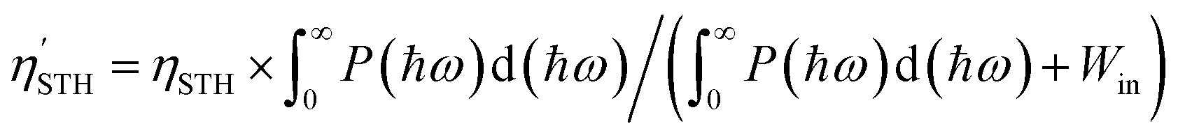 . Applying this correction, the efficiency of Ga2Ge2S3Se3 monolayer becomes 14.80%, making this monolayer a promising candidate for photon-driven water splitting photocatalysis. As mentioned above, a water splitting photocatalyst must meet many strict requirements. Therefore, to achieve the
  in the range of 3.33–16%, a monolayer is usually modified by elemental substitution, phase transitions, or the application of strain.22,59,62,93,94 The Ga2Ge2S3Se3 monolayer offers several advantages over its parent GaGeS3 monolayer.22 Notably, its solar-to-hydrogen conversion efficiency (14.80%) surpasses that of GaGeS3 (11.33%). The transition from an indirect to a direct bandgap in Ga2Ge2S3Se3 enhances light absorption and facilitates faster charge separation. While direct bandgap materials are often susceptible to rapid electron–hole recombination, this effect is mitigated in Ga2Ge2S3Se3 due to an intrinsic electric field that promotes charge separation. Consequently, the substitution of Se for S results in a monolayer with demonstrably improved photocatalytic properties.
4 Conclusion
This work employed first-principles calculations to explore potential photocatalytic water splitting materials within the A2B2X3Y3 family. Structural investigations revealed that Ga2Ge2Se3Te3 monolayer is unstable, while Ga2Ge2S3Se3 and Ga2Ge2Se3Te3 monolayers exhibit both dynamic and thermal stability. Furthermore, elastic parameter analysis demonstrates a favorable balance between flexibility and stiffness in these monolayers, making them suitable for flexible applications. Electronic structure analysis of Ga2Ge2S3Se3 and Ga2Ge2Se3Te3 monolayers indicates that orbital contributions from Ga and Y atoms within the Ga2Ge2X3Y3 formula play a crucial role in determining the bandgap values. This finding suggests a straightforward approach to tune the bandgap of Ga2Ge2X3Y3 materials, enabling a broader range of applications. While the bandgap of Ga2Ge2Se3Te3 monolayer (0.63 eV) is too narrow for efficient photocatalytic water splitting, the bandgap of Ga2Ge2S3Se3 monolayer (1.83 eV) positions it as a promising candidate. Further investigations reveal several key advantages of Ga2Ge2S3Se3 monolayer for photocatalytic water splitting applications. A significant difference of 0.27 eV in the work functions between the S-side and Se-side of the monolayer induces an intrinsic electric field, effectively driving photoexcited electrons from the Se-side to the S-side and facilitating efficient charge separation. The band edge alignment of Ga2Ge2S3Se3 monolayer is well-suited for triggering the photoexcited redox reactions involved in water splitting. This photocatalytic activity is maintained under moderate compressive strains (−6% to −8%) and tensile strains below 4%. Moreover, the Ga2Ge2S3Se3 monolayer demonstrates the capability to initiate the oxygen evolution reaction (OER) under light irradiation, releasing electrons and protons (H+) for the hydrogen evolution reaction (HER) to occur at low overpotential. The Ga2Ge2S3Se3 monolayer, even with a moderate solar-to-hydrogen efficiency of 14.80%, holds significant potential as a photocatalyst for water splitting, particularly when considering its other advantageous properties.Data availability
The data that support the findings of this study are available from the corresponding author upon reasonable request.Conflicts of interest
There are no conflicts of interest to declare.References
- R. Li, Y. Weng, X. Zhou, X. Wang, Y. Mi, R. Chong, H. Han and C. Li, Energy Environ. Sci., 2015, 8, 2377–2382 RSC.
- Y. Li, C. Liao and S. C. Tjong, Int. J. Mol. Sci., 2020, 21, 8836 CrossRef CAS PubMed.
- N. Arif, M. N. Zafar, M. Batool, M. Humayun, M. A. Iqbal, M. Younis, L. Li, K. Li and Y.-J. Zeng, J. Mater. Chem. C, 2024, 12, 12653–12691 RSC.
- Z. Chang, J. Zhang, W. Dong, X. Meng, H. Wang, D. Wei and Y. Ren, RSC Adv., 2020, 10, 37820–37825 Search PubMed.
- H. Yu, X. Huang, P. Wang and J. Yu, J. Phys. Chem. C, 2016, 120, 3722–3730 CrossRef CAS.
- M. Jothibas, S. Johnson Jeyakumar, C. Manoharan, I. Kartharinal Punithavathy, P. Praveen and J. Prince Richard, J. Mater. Sci.: Mater. Electron., 2017, 28, 1889–1894 CrossRef CAS.
- J. Pan, X. Shao, X. Xu, J. Zhong, J. Hu and L. Ma, J. Phys. Chem. C, 2020, 124, 6580–6587 CrossRef CAS.
- D. Bhanderi, P. Lakhani and C. K. Modi, RSC Sustainability, 2024, 2, 265–287 RSC.
- P. Gomez-Romero, A. Pokhriyal, D. Rueda-García, L. N. Bengoa and R. M. González-Gil, Chem. Mater., 2023, 36, 8–27 CrossRef PubMed.
- V. Kumar, G. Prasad Singh, M. Kumar, A. Kumar, P. Singh, A. K. Ansu, A. Sharma, T. Alam, A. S. Yadav and D. Dobrotă, ACS Omega, 2024, 9, 6147–6164 Search PubMed.
- W. Xu, R. Wang, B. Zheng, X. Wu and H. Xu, J. Phys. Chem. Lett., 2019, 10, 6061–6066 CrossRef CAS PubMed.
- P. Ganguly, S. Mathew, L. Clarizia, S. Kumar R, A. Akande, S. J. Hinder, A. Breen and S. C. Pillai, ACS Omega, 2019, 5, 406–421 CrossRef PubMed.
- M. M. Khan and A. Rahman, Catalysts, 2022, 12, 1338 CrossRef CAS.
- M. A. Susner, M. Chyasnavichyus, M. A. McGuire, P. Ganesh and P. Maksymovych, Adv. Mater., 2017, 29, 1602852 CrossRef PubMed.
- F. Wang, T. A. Shifa, P. Yu, P. He, Y. Liu, F. Wang, Z. Wang, X. Zhan, X. Lou and F. Xia, et al., Adv. Funct. Mater., 2018, 28, 1802151 CrossRef.
- R. Samal, G. Sanyal, B. Chakraborty and C. S. Rout, J. Mater. Chem. A, 2021, 9, 2560–2591 RSC.
- Y. Dedkov, M. Yan and E. Voloshina, Chem. Phys. Lett., 2020, 754, 137627 CrossRef CAS.
- Z. Cheng, T. A. Shifa, F. Wang, Y. Gao, P. He, K. Zhang, C. Jiang, Q. Liu and J. He, Adv. Mater., 2018, 30, 1707433 Search PubMed.
- V. Kumar, K. Rajput and D. R. Roy, Carbon, 2021, 172, 791–803 Search PubMed.
- M. Naseri, D. R. Salahub, T. V. Vu and H. Zakaryae, J. Mater. Chem. C, 2022, 10, 11412–11423 Search PubMed.
- A. Jalil, S. Z. Ilyas, S. Agathopoulos, A. Qureshi, I. Ahmed and T. Zhao, Appl. Surf. Sci., 2021, 565, 150588 Search PubMed.
- P. D. Trung and H. D. Tong, RSC Adv., 2024, 14, 15979–15986 Search PubMed.
- A.-Y. Lu, H. Zhu, J. Xiao, C.-P. Chuu, Y. Han, M.-H. Chiu, C.-C. Cheng, C.-W. Yang, K.-H. Wei and Y. Yang, et al., Nat. Nanotechnol., 2017, 12, 744–749 CrossRef CAS PubMed.
- Z. Feng, Y. Huang, S. Lin, H. Yuan and H. Chen, J. Chem. Phys., 2023, 159, 044115 CrossRef CAS PubMed.
- P. Giannozzi, S. Baroni, N. Bonini, M. Calandra, R. Car, C. Cavazzoni, D. Ceresoli, G. L. Chiarotti, M. Cococcioni and I. Dabo, J. Phys.:Condens. Matter, 2009, 21, 395502 CrossRef PubMed.
- J. P. Perdew, K. Burke and M. Ernzerhof, Phys. Rev. Lett., 1997, 78, 1396 CrossRef CAS.
- J. Heyd, G. E. Scuseria and M. Ernzerhof, J. Chem. Phys., 2003, 118, 8207–8215 CrossRef CAS.
- G. Kresse and D. Joubert, Phys. Rev. B:Condens. Matter Mater. Phys., 1999, 59, 1758 CrossRef CAS.
- S. Grimme, J. Comput. Chem., 2006, 27, 1787–1799 CrossRef CAS PubMed.
- A. Togo, L. Chaput and I. Tanaka, Phys. Rev. B:Condens. Matter Mater. Phys., 2015, 91, 094306 CrossRef.
- J. Bardeen and W. Shockley, Phys. Rev., 1950, 80, 72 CrossRef CAS.
- T. V. Vu, A. Kartamyshev, M. D. Nguyen, K. D. Pham, T. T. Trinh, N. P. Nhuan and N. D. Hien, Mater. Sci. Semicond. Process., 2024, 181, 108590 CrossRef CAS.
- F. A. Rasmussen and K. S. Thygesen, J. Phys. Chem. C, 2015, 119, 13169–13183 CrossRef CAS.
- I. Khan and J. Hong, Nanotechnology, 2020, 31, 195704 CrossRef CAS PubMed.
- M. K. Mohanta and A. De Sarkar, ACS Appl. Mater. Interfaces, 2020, 12, 18123–18137 CrossRef CAS PubMed.
- Y. Guo, S. Zhou, Y. Bai and J. Zhao, Appl. Phys. Lett., 2017, 110, 163102 CrossRef.
- M. Born and K. Huang, Dynamical Theory of Crystal Lattices, Oxford University Press, 1996 Search PubMed.
- E. Cadelano, P. L. Palla, S. Giordano and L. Colombo, Phys. Rev. B:Condens. Matter Mater. Phys., 2010, 82, 235414 CrossRef.
- J. Guo, R. Peng, X. Zhang, Z. Xin, E. Wang, Y. Wu, C. Li, S. Fan, R. Shi and K. Liu, Small, 2023, 19, 2300766 CrossRef CAS PubMed.
- P. V. Sarma, R. Nadarajan, R. Kumar, R. M. Patinharayil, N. Biju, S. Narayanan, G. Gao, C. S. Tiwary, M. Thalakulam and R. N. Kini, et al., 2D Mater., 2022, 9, 045004 CrossRef CAS.
- L.-C. Zhang, G. Qin, W.-Z. Fang, H.-J. Cui, Q.-R. Zheng, Q.-B. Yan and G. Su, Sci. Rep., 2016, 6, 19830 CrossRef CAS PubMed.
- L. Guo, H. Yan, Q. Moore, M. Buettner, J. Song, L. Li, P. T. Araujo and H.-T. Wang, Nanoscale, 2015, 7, 11915–11921 RSC.
- J. Tao, W. Shen, S. Wu, L. Liu, Z. Feng, C. Wang, C. Hu, P. Yao, H. Zhang and W. Pang, et al., ACS Nano, 2015, 9, 11362–11370 CrossRef CAS PubMed.
- A. Falin, Q. Cai, E. J. Santos, D. Scullion, D. Qian, R. Zhang, Z. Yang, S. Huang, K. Watanabe and T. Taniguchi, et al., Nat. Commun., 2017, 8, 15815 CrossRef CAS PubMed.
- J. W. Christopher, M. Vutukuru, D. Lloyd, J. S. Bunch, B. B. Goldberg, D. J. Bishop and A. K. Swan, J. Microelectromech. Syst., 2019, 28, 254–263 CAS.
- L. Yu, Q. Yan and A. Ruzsinszky, Nat. Commun., 2017, 8, 1–8 CrossRef CAS PubMed.
- H. Yi, P. Solís-Fernández, H. Hibino and H. Ago, Nanoscale Adv., 2022, 4, 3786–3792 RSC.
- B. Dong, Z. Wang, N. T. Hung, A. R. Oganov, T. Yang, R. Saito and Z. Zhang, Phys. Rev. Mater., 2019, 3, 013405 CrossRef CAS.
- L. Zhang, Y. Zhao, Y. Liu and G. Gao, Nanoscale, 2023, 15, 18910–18919 RSC.
- L. Zhang, Y. Liu, M. Wu and G. Gao, Adv. Funct. Mater., 2024, 2417857 CrossRef.
- A. K. Geim and I. V. Grigorieva, Nature, 2013, 499, 419–425 CrossRef CAS PubMed.
- M. Sledzinska, G. Jumbert, M. Placidi, A. Arrighi, P. Xiao, F. Alzina and C. M. Sotomayor Torres, ACS Appl. Electron. Mater., 2020, 2, 1169–1175 CrossRef CAS.
- A. K. Katiyar, A. T. Hoang, D. Xu, J. Hong, B. J. Kim, S. Ji and J.-H. Ahn, Chem. Rev., 2023, 124, 318–419 CrossRef PubMed.
- L. Yang, Q. Fu, W. Wang, J. Huang, J. Huang, J. Zhang and B. Xiang, Nanoscale, 2015, 7, 10490–10497 RSC.
- C. Gao, X. Yang, M. Jiang, L. Chen, Z. Chen and C. V. Singh, Phys. Chem. Chem. Phys., 2022, 24, 4653–4665 RSC.
- G. Wei, D. A. Czaplewski, E. J. Lenferink, T. K. Stanev, I. W. Jung and N. P. Stern, Sci. Rep., 2017, 7, 3324 CrossRef PubMed.
- F. Zhou, Y. Liu, Z. Lai, M. Liao, Y. Zhou, Y. Huang and J. Zhu, RSC Adv., 2018, 8, 20477–20482 RSC.
- A. Fujishima and K. Honda, Nature, 1972, 238, 37–38 CrossRef CAS PubMed.
- M. K. Mohanta and P. Jena, J. Mater. Chem. C, 2024, 12, 1888–1896 RSC.
- D. Er, H. Ye, N. C. Frey, H. Kumar, J. Lou and V. B. Shenoy, Nano Lett., 2018, 18, 3943–3949 CrossRef CAS PubMed.
- M. C. Toroker, D. K. Kanan, N. Alidoust, L. Y. Isseroff, P. Liao and E. A. Carter, Phys. Chem. Chem. Phys., 2011, 13, 16644–16654 RSC.
- Q.-W. He, J.-H. Wang, D.-Y. Zhu, D.-S. Tang, Z. Lv, F. Guo and X.-C. Wang, Nano Lett., 2024, 24, 8979–8987 CrossRef CAS PubMed.
- Z. Wang and G. Zhou, J. Phys. Chem. C, 2019, 124, 167–174 CrossRef.
- S. Singh, P. Anees, S. Chandra and T. K. Ghanty, J. Phys. Chem. C, 2022, 126, 8436–8449 CrossRef CAS.
- Z. Liu, B. Wang and C. Cazorla, ACS Sustain. Chem. Eng., 2022, 10, 16924–16934 CrossRef CAS.
- X.-H. Li, B.-J. Wang, X.-L. Cai, W.-Y. Yu, L.-W. Zhang, G.-D. Wang and S.-H. Ke, RSC Adv., 2017, 7, 44394–44400 RSC.
- L. Ju, J. Shang, X. Tang and L. Kou, J. Am. Chem. Soc., 2019, 142, 1492–1500 CrossRef PubMed.
- N. Vonrüti and U. Aschauer, Phys. Rev. Mater., 2018, 2, 105401 CrossRef.
- M. Pandey, C. Pandey, R. Ahuja and R. Kumar, Nano Energy, 2023, 109, 108278 CrossRef CAS.
- L.-B. Shi, S. Cao and M. Yang, Phys. E, 2019, 107, 124–130 CrossRef CAS.
- R. Roldán, A. Castellanos-Gomez, E. Cappelluti and F. Guinea, J. Phys.: Condens. Matter, 2015, 27, 313201 CrossRef PubMed.
- Y. Jiao, F. Ma, G. Gao, J. Bell, T. Frauenheim and A. Du, J. Phys. Chem. Lett., 2015, 6, 2682–2687 CrossRef CAS PubMed.
- X. Zhang, X. Zhang, P. M. Ajayan, J. Wen and H. D. Espinosa, Small, 2022, 18, 2105194 CrossRef CAS PubMed.
- E. Blundo, E. Cappelluti, M. Felici, G. Pettinari and A. Polimeni, Appl. Phys. Rev., 2021, 8, 021318 CAS.
- X. Peng, Q. Wei and A. Copple, Phys. Rev. B:Condens. Matter Mater. Phys., 2014, 90, 085402 CrossRef CAS.
- D. D. Vo, T. V. Vu, A. Kartamyshev, T. H. Ho and N. N. Hieu, Nanoscale Adv., 2024, 6, 6019–6028 RSC.
- J. K. Nørskov, T. Bligaard, A. Logadottir, J. Kitchin, J. G. Chen, S. Pandelov and U. Stimming, J. Electrochem. Soc., 2005, 152, J23 CrossRef.
- C. Quan, S. Ji, R. Yao, W. Liu, J. Yang and X. Li, Int. J. Hydrogen Energy, 2024, 56, 1227–1234 CrossRef CAS.
- T. V. Vu, N. N. Hieu, D. D. Vo, A. Kartamyshev, H. D. Tong, T. T. Trinh, V. Khuong Dien, Z. Haman, P. Dey and N. Khossossi, J. Phys. Chem. C, 2024, 128, 4245–4257 CrossRef CAS.
- L. Ju, M. Bie, X. Tang, J. Shang and L. Kou, ACS Appl. Mater. Interfaces, 2020, 12, 29335–29343 CAS.
- Y. Sun, A. Huang and Z. Wang, RSC Adv., 2019, 9, 26321–26326 RSC.
- Q. Cai, W. Hong, C. Jian, X. He and W. Liu, Adv. Energy Sustainability Res., 2023, 4, 2200178 CrossRef CAS.
- D. W. Boukhvalov, S. Nappini, M. Vorokhta, T. O. Menteş, L. Piliai, M. Panahi, F. Genuzio, J. De Santis, C.-N. Kuo and C. S. Lue, et al., Adv. Funct. Mater., 2021, 31, 2106228 CrossRef CAS.
- Y. Chen, X. Fu and Z. Peng, Metals, 2023, 13, 1163 CrossRef CAS.
- L. M. Herz, ACS Energy Lett., 2017, 2, 1539–1548 CrossRef CAS.
- D. Shi, V. Adinolfi, R. Comin, M. Yuan, E. Alarousu, A. Buin, Y. Chen, S. Hoogland, A. Rothenberger and K. Katsiev, et al., Science, 2015, 347, 519–522 CrossRef CAS PubMed.
- Y. Cai, G. Zhang and Y.-W. Zhang, J. Am. Chem. Soc., 2014, 136, 6269–6275 CrossRef CAS PubMed.
- Y. Wang, Y. Li and Z. Chen, J. Mater. Chem. C, 2015, 3, 9603–9608 RSC.
- C. Long, Y. Liang, H. Jin, B. Huang and Y. Dai, ACS Appl. Energy Mater., 2018, 2, 513–520 CrossRef.
- Y. Jing, Z. Zhou, J. Zhang, C. Huang, Y. Li and F. Wang, Phys. Chem. Chem. Phys., 2019, 21, 21064–21069 RSC.
- X. Liu, Z. Zhang, Z. Ding, B. Lv, Z. Luo, J.-S. Wang and Z. Gao, Appl. Surf. Sci., 2021, 542, 148665 CrossRef CAS.
- X. Liu, W. Kang, J. Zhao, Y. Wang, W. Wang, L. Wang, L. Fang, Q. Chen and M. Zhou, Phys. Status Solidi RRL, 2022, 16, 2100417 CrossRef CAS.
- P. Jamdagni, A. Kumar, S. Srivastava, R. Pandey and K. Tankeshwar, Phys. Chem. Chem. Phys., 2022, 24, 22289–22297 RSC.
- K. Chaoui, W. Elaggoune and K. Zanat, Int. J. Hydrogen Energy, 2024, 91, 1221–1231 CrossRef CAS.
Footnote |
| † Electronic supplementary information (ESI) available. See DOI: https://doi.org/10.1039/d5ra00812c |
| This journal is © The Royal Society of Chemistry 2025 |