
 Open Access Article
 This Open Access Article is licensed under a Creative Commons Attribution-Non Commercial 3.0 Unported Licence
Thickness-dependent performance of antimony sulfide thin films as a photoanode for enhanced photoelectrochemical water splitting
D. M. Kavya a,
Y. N. Sudhakarb,
A. Timoumic and
Y. Raviprakash*a
a,
Y. N. Sudhakarb,
A. Timoumic and
Y. Raviprakash*a
aDepartment of Physics, Manipal Institute of Technology, Manipal Academy of Higher Education, Manipal-576104, India. E-mail: raviprakash.y@manipal.edu
bDepartment of Chemistry, Manipal Institute of Technology, Manipal Academy of Higher Education, Manipal, 576104, Karnataka, India
cDepartment of Physics, Faculty of Science, Umm Al-Qura University, 21955, Makkah, Saudi Arabia
First published on 28th April 2025
Abstract
A two-step synthesis approach is employed for antimony sulfide thin films, which includes thermal evaporation followed by annealing in a sulfur atmosphere using chemical vapor deposition (CVD). The thickness of the films is systematically varied to study its impact on the material's properties. The orthorhombic crystal structure of each film is verified by Grazing Incidence X-ray Diffraction (GIXRD) analysis. Raman spectroscopy reveals thickness-dependent changes in the vibrational properties. Surface morphology and roughness are examined using atomic force microscopy (AFM) and field emission scanning electron microscopy (FESEM), with findings indicating that layer thickness significantly affects these surface characteristics. Energy-dispersive X-ray spectroscopy (EDS) and X-ray photoelectron spectroscopy (XPS) demonstrate that variations in film thickness influence the surface chemical composition and oxidation states. The Sb2S3 thin film with a thickness of 450 nm exhibited a band gap of 1.75 eV, indicating its potential for efficient light absorption. It also demonstrated a conductivity of 0.006 mA at an applied voltage of 1 V, reflecting its electrical transport properties. Furthermore, the film achieved a current density of 0.70 mA cm−2, signifying enhanced charge transfer efficiency. These findings suggest that the 450 nm thick film offers an optimal balance of band gap, light absorption, and photocurrent density, making it the most suitable candidate for photoelectrochemical water-splitting applications.
1. Introduction
Advancements in materials science are crucial for enhancing renewable energy technologies, particularly in the growth of resourceful, durable, and cost-effective materials for hydrogen energy production. A key area of focus is the improvement of photocatalysts and electrode materials to upsurge the effectiveness and scalability of water splitting. These resources must exhibit desirable properties such as nanostructures, low band gaps, and low resistivity to optimize their performance in photoelectrochemical (PEC) applications.1 Significant research has been directed towards metal oxides, nitrides, and chalcogenides, each offering unique advantages and limitations. Meanwhile, metal oxides and nitrides possess high band gaps that limit their practical application.2–5 Chalcogenide compounds containing group 16 elements such as sulfur, selenium, and tellurium have emerged as promising alternatives due to their excellent optical properties, including high absorption coefficients and low band gaps.6,7 Transition metal dichalcogenides, including materials like MoS2, WS2, MoSe2, WSe2, Sb2S3, and Sb2Se3 are particularly suited for water splitting because of their optimal band gaps (1–2 eV) and outstanding light absorption capabilities.8,9Among these antimony(III) sulfide (Sb2S3) films have attracted significant attention as promising alternative photocathodes for hydrogen generation in PEC cells. This interest stems from their distinct optoelectronic properties, including a narrow optical bandgap (Eg) of 1.7 eV and a high absorption coefficient (α) of 104–105 cm−1 for photons with energy exceeding the bandgap.10 Additionally, Sb2S3 offers a high theoretical maximal photocurrent density of around 24.5 mA cm−2 and an impressive theoretical solar-to-hydrogen efficiency of 28%, making it highly attractive for practical applications.11 However, challenges such as insufficient absorption in thin films due to inadequate thickness, interference effects, and low material density, as well as issues related to inhomogeneity, internal scattering, and stress-induced defects in thicker films, can hinder absorption efficiency.12
Recent research has shown how important film thickness is in determining the performance of Ag3SbS3 thin films in PEC applications, with a 700 nm thick film demonstrating a photo-conversion efficiency of 0.68%, outperforming other materials.13 Additionally, research into the impact of photoanode thickness reveals that thinner photoanodes induce polarized states, increasing surface trapping and shortening the lifetime of photogenerated charges. Conversely, thicker photoanodes facilitate the removal of unstable surface layers, promoting oxygen evolution while preserving the integrity of the solid–solid interface.14
In this study, we explore how Sb2S3 thin film thickness influences morphology, elemental composition, and optical, electrical, and electrochemical properties in PEC water splitting. We aim to elucidate its role in charge transfer mechanisms, conductivity processes, and overall photoanode efficiency.
Our findings indicate that optimizing film thickness enhances charge transfer efficiency by stabilizing the interface and exposing active sites for oxygen evolution. This approach mitigates exciton recombination caused by deep-level defects in Sb2S3, enhancing PEC performance. The optimized Sb2S3 photoelectrode achieves a photocurrent density of 0.7 mA cm−2, surpassing the bare electrode (0.6 mA cm−2).15 These findings provide a fundamental understanding of thickness-dependent charge transport mechanisms and offer a promising strategy for designing efficient Sb2S3-based photoanodes for solar-driven water splitting. These results provide crucial insights into thickness-dependent charge transport and offer a promising strategy for designing efficient Sb2S3-based photoanodes for solar-driven water splitting.
This work represents the first investigation into the role of Sb2S3 film thickness in PEC water-splitting applications. While Sb2S3 has been explored for various other applications, including photovoltaics,16 photosensitization of wide bandgap semiconductors,17 photocatalytic environmental remediation,18 battery storage,19 and even PEC solar cells.20 Previously, it had been proposed to be an inactive water-splitting photocatalyst. In this work, we demonstrate how to optimize photocurrent density by varying film thickness. Despite facing challenges with photo-corrosion, we hypothesize that shielding Sb2S3 from degradation could improve its viability as a top cell absorber in devices, potentially through doping21 or heterojunction engineering.22 We identified three key areas for enhancement: morphology, stoichiometry, and optical properties. These improvements can be pursued by optimizing the film thickness, annealing in a sulfur atmosphere,23 and applying doping techniques.24
2. Experimental details
Antimony sulfide (Sb2S3) films were deposited by thermal evaporation using a fluorine-doped tin oxide-coated (FTO) glass substrate as the substrate and a molybdenum boat as the source holder. After ten minutes of ultrasonic cleaning in isopropyl alcohol, the substrates were dried with nitrogen purging before deposition. Cleaned substrate, and high-purity antimony sulfide (Sb2S3) powder (Thermo Fisher, 99.9%) was then placed into the thermal evaporation chamber. 5 × 10⁻⁶ mbar was the average pressure, which was maintained via liquid nitrogen, with a standoff distance of 16 cm between the source and the substrate. The substrate temperature was set to 150 °C during deposition. The deposition rate and film thickness were controlled and measured using a digital quartz crystal monitor. By setting the filament current to 85 A, the deposition rate was maintained between 3.5 and 4 Å s−1, with the final film thickness varying from approximately 350–500 nm. Following deposition, a custom chemical vapor deposition (CVD) apparatus was used to sulfurize (annealing in sulfur atmosphere) the films for 30 minutes at 400 °C under 900 mbar of vacuum. 100 mg of sulfur (Thermo Fisher, 99.9998% purity) was evaporated in a single-zone furnace with a nitrogen environment as defined in our previous work.23 Following sulfurization, the films were cooled to room temperature under vacuum conditions. Film thicknesses were measured via a stylus profilometer (Bruker Dektak profilometer) and the experimental values are provided in Table 1.| Sample name | Thickness (nm) ± 10 nm |
|---|---|
| T1 | 350 |
| T2 | 400 |
| T3 | 450 |
| T4 | 500 |
3. Characterizations
Structural analysis of the antimony sulfide (Sb2S3) films was carried out using Grazing Incidence X-ray diffraction (GIXRD). Data was obtained with a Bruker AXS D8 Advance Diffractometer utilizing Cu Kα radiation over an angular range of 10–60° with a scanning rate of 0.1° min−1 at room temperature. Raman spectroscopy was conducted in a backscattering configuration with a Nd: YVO4 diode-pumped solid-state laser, employing a 532 nm excitation wavelength. The surface morphology was examined through scanning electron microscopy (SEM) (Zeiss EVO MA18) with an acceleration voltage of 10 kV, and the elemental composition was analyzed via energy-dispersive X-ray spectroscopy (EDS) (Oxford INCA X-act). X-ray photoelectron spectroscopy (XPS) measurements were performed with a SPECS (Germany) X-ray photoelectron spectroscope utilizing Al Kα (1486.61 eV) radiation and applying a 13 kV anode voltage. The surface topography was investigated via atomic force microscopy (AFM) with the tapping mode Flex-Axiom AFM. Optical absorption spectra were obtained via a UV-visible spectrophotometer (Shimadzu UV-1900) over the range of 190–1100 nm. Photoluminescence measurements were carried out with a fluorescence spectrometer using a Nd: YVO4 diode-pumped solid-state laser with an excitation wavelength of 420 nm.The PEC performance of the photoelectrodes was measured using a CompactStat.h, IVIUM potentiostat connected to a standard three-electrodes PEC H-cell from Redox.me. The antimony sulfide thin film, platinum (Pt) wire, and Ag/AgCl electrode were used as working, counter, and reference electrodes, respectively. A 0.1 M Na2SO4 aqueous solution (pH = 7) was used as the electrolyte. The potential relative to the reversible hydrogen electrode (RHE) was calculated via the appropriate conversion formula.

 vs. NHE at 28 °C.
The light source for PEC experiments was a 1-Sun LED Solar Simulator (Redoxme), providing a light intensity of 100 mW cm−2. The films were exposed in a back side illumination geometry the exposed area was 0.5 cm2. Photocurrent was recorded as a function of the voltage using linear sweep voltammetry (LSV) with a scan rate of 50 mV s−1. Electrochemical impedance spectroscopy (EIS) was performed over a frequency range of 0.1 Hz to 100 kHz at 0.5 V sinusoidal voltage.
4. Results and discussion
4.1 Structural analysis
The Grazing Incidence X-ray diffraction (GIXRD) patterns of antimony sulfide (Sb2S3) are shown in Fig. 1 and are referenced to the standard JCPDS card (no. 42-1393). All samples, display an intense peak at 24.9° corresponding to the (1 3 0) orientation plane, revealing the orthorhombic stibnite structure of Sb2S3. The enhanced intensity of the (1 3 0) peak with increasing film thickness (i.e., longer deposition time) indicates preferential growth along the (1 3 0) crystallographic direction. This indicates that as the deposition time increases, the film growth mechanism favors alignment along the (1 3 0) plane, resulting in enhanced crystallographic orientation and increased peak intensity for this plane in the grazing incidence X-ray diffraction pattern.25 Additionally, sample T2 showed a peak shift to a lower angle. This observed shift can be attributed to several factors. Compositional gradients, which involve variations in the film's composition, can alter the lattice parameters and affect the peak positions. Additionally, internal strain and variation in the lattice spacing resulted in a shift in the XRD peaks. Together, these factors reflect structural changes within the material, as indicated by the peak shift.26 | ||
| Fig. 1 GIXRD patterns of antimony sulfide films. | ||
Table 2 lists the crystallographic parameters of the antimony sulfide films with various thicknesses. The data show a trend where increasing film thickness generally results in larger crystallite sizes and reduced microstrain. The observed decrease in microstrain suggests fewer lattice imperfections, as supported via the reduction of grazing incidence X-ray diffraction (GIXRD) peaks and enhance the crystallite size with increasing film thickness.27 However, an anomaly is noted in sample T2, where the crystallite size unexpectedly decreases and the microstrain increases. This increase in microstrain for sample T2 may have contributed to a shift toward lower diffraction angles in the XRD patterns.28 Furthermore, the lattice parameters vary with thickness, and for samples T3 and T4, these parameters closely match the expected values for antimony sulfide films.
| Sample | Crystallite size D (nm) | Microstrain, ε (×10−3) | Dislocation density, δ (×1015/m2) | Interplanar distance, dhkl (Å) | Lattice parameters (Å) | ||
|---|---|---|---|---|---|---|---|
| a (11.22) | b (11.31) | c (3.83) | |||||
| T1 | 18.0 | 8.9 | 3.0 | 3.58 | 11.3 | 11.47 | 3.87 |
| T2 | 14.6 | 10.6 | 4.6 | 3.59 | 11.01 | 11.23 | 3.74 |
| T3 | 19.4 | 8.2 | 2.6 | 3.64 | 11.18 | 11.38 | 3.78 |
| T4 | 19.8 | 8.07 | 2.5 | 3.64 | 11.24 | 11.42 | 3.83 |
Fig. 2 presents the Raman spectra of the antimony sulfide films, which show distinct modes at 109, 125, 146, 186, 238, 280, 300, and 495 cm−1.29,30 The mode at 495 cm−1 is assigned to the FTO substrate.31 Specifically, the modes at 109, 154, 186, and 280 cm−1 correspond to the Ag modes, while the modes at 238 and 300 cm−1 are related to the B1g/B3g modes. We can see the variation in the intensity with respect to the thickness. This variation in Raman intensity with variation in crystallite size occurs because larger crystallites have better scattering efficiency and fewer structural defects. In larger crystallites, more photons interact with the lattice, leading to stronger Raman signals. Additionally, reduced defects and less phonon confinement in larger crystals result in sharper and more intense Raman peaks.32 Here, we can observe that sample T2 has the highest intensity and shifts toward the lower side compared with the other samples. This may be due to the microstrain, which we observed via XRD. Microstrain generally affects Raman scattering by causing peak shifts due to distortions in the lattice structure. While it can alter the Raman spectra, it does not typically enhance the intensity directly. Instead, factors such as an optimal crystallite size and fewer defects often play a larger role in increasing the intensity.33 XRD and Raman analyses showed that all the obtained samples were single-phase antimony sulfide.
 | ||
| Fig. 2 Raman spectra of antimony sulfide films. | ||
4.2 Morphological and topographical analysis
Fig. 3 shows the morphology obtained through field emission scanning electron microscopy (FESEM). In samples T2 and T4 compact formation of grains is evident. In contrast, samples T1 and T3 display island-like structures. The noted changes in morphology with varying film thickness are likely attributable to alterations in grain size as the thickness increases due to extended deposition times, which allow grains to grow and coalesce. This variation in grain size could also be influenced by the change in adhesion properties of the molecules at different thicknesses, leading to the observed morphological differences.34 | ||
| Fig. 3 FESEM images of antimony sulfide films. | ||
Fig. 4 represents images of atomic force microscopy (AFM) that highlight the variations in surface morphology across the different samples. As the thickness of the samples changes, there is a corresponding variation in surface roughness, as indicated by the roughness parameters [average roughness (Ra) and root mean square roughness (Rq)] provided in Table 3. The notable differences in roughness are likely attributable to the morphological changes observed in Fig. 3. Specifically, sample T2 is rougher than samples T1, T3, and T4. The increased roughness at T2, as discussed in the morphological analysis, may be attributed to variations in deposition time, potentially influencing the adhesion properties of molecules at different thicknesses, thereby affecting film roughness.35 It is further confirmed that the shifts toward lower angles observed in the XRD patterns, compared to other samples, could be attributed to the presence of the highest microstrain, as revealed by XRD analysis.
 | ||
| Fig. 4 AFM images of antimony sulfide films. | ||
| Sample name | Ra (nm) ± 2 nm | Rq (nm) ± 2 nm |
|---|---|---|
| T1 | 26.0 | 45.0 |
| T2 | 72.6 | 103.4 |
| T3 | 37.1 | 59.6 |
| T4 | 22.4 | 33.6 |
4.3 Compositional analysis
Energy-dispersive spectroscopy (EDS) was employed to conduct elemental analysis on the deposited antimony sulfide films. Table 4 provides the atomic percentage compositions of the films. Notably, the Sb to S (Sb![[thin space (1/6-em)]](https://www.rsc.org/images/entities/char_2009.gif) :S) atomic ratio exhibited variability corresponding to changes in film thickness. Specifically, sample T3 had an Sb:S ratio of 2:3.5, which closely approximates the expected stoichiometric ratio of 2:3.
:S) atomic ratio exhibited variability corresponding to changes in film thickness. Specifically, sample T3 had an Sb:S ratio of 2:3.5, which closely approximates the expected stoichiometric ratio of 2:3.
| Sample name | Atomic percentage (%) | ||
|---|---|---|---|
| Sb (40) | S (60) | S/Sb | |
| T1 | 20 | 80 | 4 |
| T2 | 33 | 67 | 2 |
| T3 | 25 | 75 | 3 |
| T4 | 34 | 66 | 1.9 |
X-ray photoelectron spectroscopy (XPS) was employed to analyze the chemical composition of the surface of the samples. The binding energy peaks were deconvoluted via a Gaussian–Lorentzian function. Before data analysis, all spectra were referenced to the C 1s peak at 284.6 eV for calibration Fig. 5(a) displays the survey spectra of antimony sulfide films of various thicknesses. Fig. 5(b) presents the Sb 3d core spectra, illustrating a doublet of peaks at 528.9 eV (3d5/2) and 538.2 eV (3d3/2).15 The 9.4 eV splitting of the Sb 3d doublet indicates the presence of trivalent antimony (Sb3+) in Sb2S3.36 The area ratio of the 3d5/2 peak to the 3d3/2 peak is approximately 1.5 (3:2), which is consistent with the expected ratio.37 The two shoulder peaks observed at 529.2 eV and 530.9 eV depict the Sb 3d5/2 and Sb 3d3/2 of Sb2O3, respectively, also showing a peak separation of 9.4 eV and an area ratio of 1.5. The peak at 532 eV reveals the presence of oxygen (O) in its 1s state.38 These oxygen impurities are likely introduced during the sulfurization process due to residual oxygen in the tube furnace.39 Fig. 5(c) presents the S 2p core spectra of the antimony sulfide films. In the sulfur spectrum, two overlapping peaks at 160.8 eV and 161.9 eV correspond to the 2p3/2 and 2p1/2 states, respectively. The area under the curve ratio of 2p3/2 to 2p1/2 is 2:1, with an energy separation of 1.1 eV, indicating the S2− oxidation state.40,41 The S 2p peaks at 163 eV and 164 eV (S 2p3/2 and S 2p1/2) correspond to sulfur bound to oxygen, indicating the presence of sulfur oxides and sulfates.42 From both core spectra, it is evident that higher binding energy generally correlates with higher oxidation states of the material.40 The XPS results demonstrate that these oxide states are present on the surface of the sample, likely because of surface oxidation. This finding has been confirmed by the XRD pattern and Raman spectra showing no oxide peaks.43
 | ||
| Fig. 5 (a) Survey spectra, (b) & (c) core spectra of Sb 3d and S 2p of the antimony sulfide film. | ||
4.4 Optical analysis
Fig. 6 represents (a) absorbance spectra, (b) absorption coefficient spectra, (c) Tauc plots, and (d) photoluminescence spectra of antimony sulfide films. Table 5 provides the band gap values for each sample as deduced from Tauc plot fit. The analysis shows that both the absorbance and absorption spectra in Fig. 6(a) and (b) exhibit variations related to the thickness of the samples. Band gap values were obtained from the Tauc plots, as illustrated in Fig. 6. These are listed in Table 5 for each sample. | ||
| Fig. 6 (a) Absorbance spectra, (b) absorption coefficient spectra, (c) Tauc plots, and (d) photoluminescence spectra of antimony sulfide films. | ||
| Sample name | Band gap (eV) |
|---|---|
| T1 | 1.80 |
| T2 | 1.75 |
| T3 | 1.75 |
| T4 | 1.70 |
The observed variations in the absorbance and absorption coefficients are likely due to differences in the stoichiometric ratio, as indicated in Table 4. A higher atomic concentration of sulfur (T1: S/Sb = 4) leads to increased bandgap (T1 1.8 eV) because higher sulfur concentration strengthens the bonds within the material, which can shift the energy levels of the electronic states, resulting in a larger band gap.44,45 The band gap variations across the samples are attributed primarily to the incorporation of sulfur into the films and the presence of sulfur vacancies. These characteristics may cause additional electronic states to arise slightly above the valence band, thereby altering the absorption edge.46 Additionally, differences in the grain size and stoichiometric ratio, as supported by the FESEM images and EDS results in Table 4, contributed to the observed variations in the absorbance, absorption coefficient, and band gap. The stoichiometric ratio plays a crucial role in determining a material's band gap by introducing defects, altering the phase composition, and influencing atomic bonding. Deviations from ideal stoichiometry can create localized states, modify doping effects, and cause charge imbalances, leading to band gap narrowing or broadening, thus impacting the material's electronic properties.
The photoluminescence analysis was conducted to examine the optical properties of the samples. Fig. 6(d) presents the photoluminescence spectra of antimony sulfide films excited at a wavelength of 420 nm.47 Upon excitation, emission peaks in the 460 nm range were observed, indicating blue luminescence.48,49 This blue emission is attributed to donor–acceptor ion transitions, commonly linked to defects or deep trap states.29 A variation in the emission intensity with increasing film thickness was observed. These changes in emission intensity are likely due to a combination of physical thickness effects and stoichiometric variations that alter the material's electronic structure and optical behavior.50
Increasing the film thickness causes variations in both the stoichiometric ratio and crystallite size, which subsequently affect the emission intensity. According to the properties of the donor and acceptor ions, where Sb3+ represents the donor ion and S2− the acceptor ion, the films were classified into two types: antimony-rich (Sb-rich) and sulfur-rich (S-rich) films. Sb-rich films exhibit three electron trap states, termed donor defects, while S-rich films display two hole trap states, known as acceptor defects.51,52
The primary defects identified include Sb interstitial (Sbi), sulfur vacancy (Vs), antimony antisite (SbS), antimony vacancy (VSb), and sulfur antisite (SSb) defects. In Sb-rich Sb2S3, the increase in Vs is attributed to sulfur deficiency. As a result, excess Sb atoms tend to occupy Vs sites rather than interstitial positions, due to the lower formation energy of SbS compared to Sbi. Consequently, Sb-rich Sb2S3 exhibits a higher concentration of Vs and SbS defects.
In S-rich Sb2S3, sulfur atoms infiltrate the lattice and fill Vs sites. Due to the higher formation energies of SbS and Sbi defects in a sulfur-rich environment, the formation of these defects is suppressed. Instead, the S-rich condition favors the formation of significant amounts of VSb, driven by the reduced formation energy. To maintain structural stability, some sulfur atoms may occupy VSb sites, leading to the formation of SbS antisite defects.52
4.5 Electrical analysis
Fig. 7 presents the (a) linear and (b) semilogarithmic plots of the current–voltage (I–V) characteristics of the deposited antimony sulfide films. The data reveal that an increase in film thickness from T1 to T3 correlates with a significant increase in conductivity. Specifically, the T3 sample revealed a current of 0.006 mA at 1 V. This trend can be attributed to the corresponding decrease in film resistance by increasing the thickness.53,54 However, for thicknesses exceeding 450 nm, a decrease in conductivity was observed, as seen in sample T4. This reduction in conductivity is attributed to an increase in grain boundaries, as evidenced by SEM images. These structural imperfections lead to greater scattering and recombination of charge carriers, which in turn diminishes the overall conductivity.55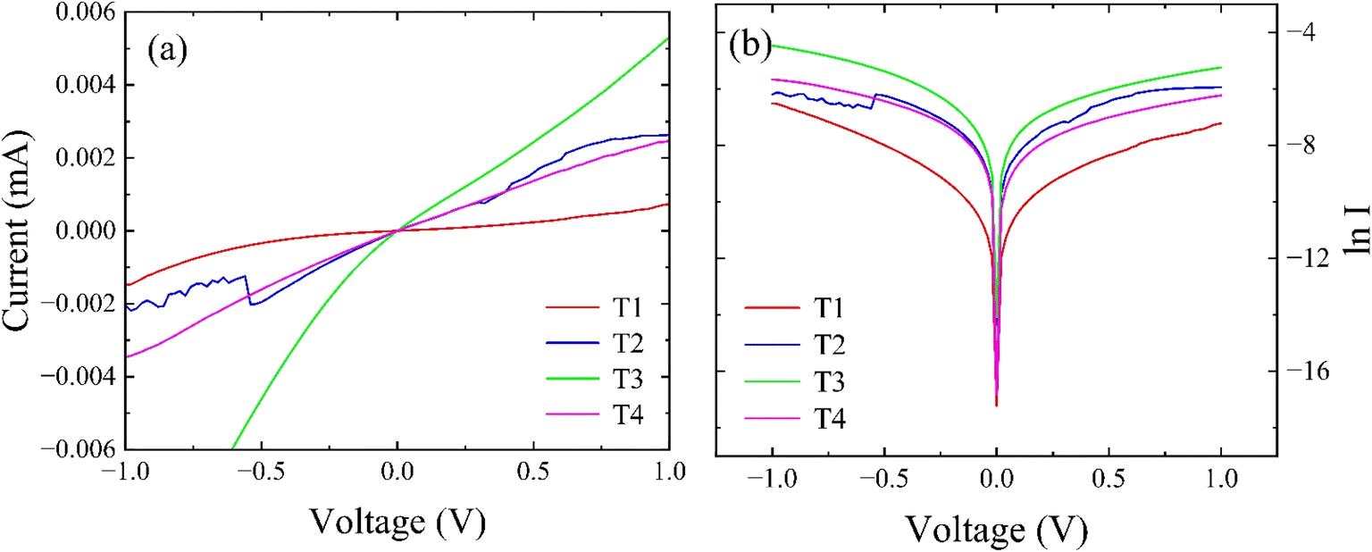 | ||
| Fig. 7 (a) Linear and (b) semilog plots of the I–V characteristics of antimony sulfide films. | ||
4.6 Electrochemical analysis
Fig. 8(a) shows the cyclic voltammetry (CV) and Nyquist plots of the antimony sulfide films. In the CV curve shown in Fig. 8(a), an oxidation peak is observed at 1.3 V versus Ag/AgCl, with the peak intensity decreasing as the film thickness increases.56 Initially, the current density increases with increasing film thickness (from T1 to T3) but for T3 it decreases. The oxidation peak in thinner films is attributed to the fact that a species undergoes oxidation during the electrochemical measurement. The variation in film current density concerning thickness is likely due to changes in conductivity, as depicted in Fig. 8. This variation in conductivity is influenced by defects and grain boundaries, which lead to increased scattering and recombination of charge carriers, ultimately affecting the complete conductivity of the films. The Nyquist plot in Fig. 8(b) representing the imaginary part of the impedance (Z′′) as a function of the real part of the impedance (Z′), provides insights into the electrochemical properties at the interface electrode/electrolyte. This interface can be modeled with an equivalent circuit containing an RSCCSC parallel circuit for the semiconductor part in series with another RHCH parallel circuit corresponding to the Helmholtz layer formed inside the electrolyte near the electrode surface. Specifically, the internal resistance depicted in the plot represents the overall resistance encountered in the course of the charge transfer process. The observed impedance behavior specifically highlights the existence of charge transfer resistance, highlighting the difficulty of electron transfer at the electrode–electrolyte interface.57 As sample thickness increases, the charge transfer resistance decreases, likely because of the higher loading of antimony sulfide. Notably, sample T3 has a lower charge transfer resistance than the other samples, likely resulting from improved conductivity and better aggregation of antimony sulfide within the film.58 The increase in charge transfer resistance observed in sample T4, as depicted in Fig. 8, may be due to the combined effects of low absorption coefficient, reduced surface roughness, and decreased electrical conductance at higher thicknesses. | ||
| Fig. 8 (a) Cyclic voltammograms and (b) Nyquist plots of deposited antimony sulfide films. | ||
The photocurrent density of antimony sulfide films varies with thickness due to changes in electrical conductivity, charge transport efficiency, and recombination processes. Fig. 9 illustrates the current density versus potential (J–V) characteristics of antimony sulfide films with varying thicknesses, measured under illuminated and dark conditions. Sample T1 exhibits a photocurrent density of 0.28 mA cm−2 at 0.2 V vs. RHE. A progressive increase in current density is observed for samples T2 and T3, attributed to enhanced electrical conductivity and improved charge transport as the film thickness increases. This increase in thickness enhances charge carrier availability, facilitating efficient charge transfer to the electrode–electrolyte interface and resulting in a higher photocurrent density from T1 to T3. However, beyond an optimal thickness (T3), further film growth (T4) leads to excessive charge carrier recombination due to longer diffusion paths and increased internal resistance, ultimately reducing the photocurrent. This decline in current density in sample T4 is likely due to excessive film thickness, which promotes recombination and impedes conductivity, as evident from Fig. 7(a). Furthermore, the J–V curves exhibit two distinct humps, which may be associated with the oxidation of the material during PEC measurements. Among all samples, T3 achieves the highest photocurrent density of 0.70 mA cm−2, which can be correlated with its superior electrical conductivity, as illustrated in Fig. 7. Enhanced conductivity generally improves charge carrier mobility, thereby accelerating charge transfer kinetics at the electrode–electrolyte interface. Consequently, this efficient charge transport contributes to an overall increase in photocurrent density, further supporting the optimization of film thickness for superior PEC performance.59 However, during the experiment, substantial degradation of the samples was observed, likely due to electrode–electrolyte interactions leading to material corrosion, which adversely affects stability.60–62 Strategies such as elemental doping or the incorporation of heterojunctions may be effective in mitigating these stability issues while simultaneously improving charge transfer kinetics.
 | ||
| Fig. 9 LSV curves of antimony sulfide films. | ||
5. Conclusions
Thermally evaporated antimony sulfide thin films deposited on FTO substrates exhibited an orthorhombic stibnite structure across all samples, with crystallite size and microstrain varying with film thickness. Film thickness significantly affected vibrational properties, particularly the T2 mode, where the 400 nm thick sample showed the highest intensity and peak shifts attributed to microstrain. Surface morphology analysis revealed that increasing thickness altered surface roughness, correlating with changes in grain size. Compositional analysis using EDS and XPS confirmed thickness-dependent stoichiometric variations and the presence of surface oxides. Among the investigated samples, the 450 nm thick film (T3) demonstrated optimal optoelectronic properties, with a band gap of 1.75 eV, high electrical conductance (0.006 mA at 1 V), and low charge transfer resistance. The obtained photocurrent density of 0.70 mA cm−2 under illumination highlighted its superior charge transport characteristics. However, surface oxidation remains a critical factor affecting long-term photocurrent stability during PEC operation. Addressing these oxidation-related challenges is essential for enhancing the durability of the film and the stability of the sample. The distinct performance of the 450 nm thick film positions it as a strong candidate for photoelectrochemical water splitting, with further optimization expected to improve its effectiveness as a photoanode in PEC applications.Data availability
The most data pertaining to this article is mentioned in the article itself. Any missing data can be provided on a reasonable request to the corresponding author.Conflicts of interest
There are no conflicts of interest to declare.Acknowledgements
The authors extend their heartfelt gratitude to Dr Dana Stanescu. Dr Dana Stanescu, SPEC, CEA, CNRS, Université Paris-Saclay, CEA Saclay, France, for valuable support with electrochemical measurements and guidance in data analysis. The authors express their gratitude to the Manipal Academy of Higher Education for providing financial support through the Dr TMA Pai PhD scholarship. Dr Sudha D. Kamath (MIT Manipal) is acknowledged for providing photoluminescence measurements. The authors thank the Indian Institute of Science Bengaluru for providing facilities through the Indian Nanoelectronics Users Program (INUP), supported by the Ministry of Human Resource Development (MHRD), Government of India. Special thanks are extended to Dr Uday Deshpande and Mr Parveen Garg from the UGC-DAE Consortium, Indore, for their assistance with XPS measurements and their valuable suggestions for data analysis. Ms. Pramitha. A, and Mr Pramod R. Nadig (Manipal Institute of Technology, Manipal) are acknowledged for their assistance with the analysis.References
- W. Chen, G. Jin, Y. Liu, Q. Wei and J. Tang, Ternary Photoanodes with AgAu Nanoclusters and CoNi-LDH for Enhanced Photoelectrochemical Water Oxidation, ACS Appl. Mater. Interfaces, 2024, 16, 23296–23304, DOI:10.1021/acsami.4c01938.
- P. J. Megia, A. J. Vizcaino, J. A. Calles and A. Carrero, Hydrogen Production Technologies: From Fossil Fuels toward Renewable Sources. A Mini Review, Energy Fuels, 2021, 35(20), 16403–16415, DOI:10.1021/acs.energyfuels.1c02501.
- J. D. Shakun, et al., Global warming preceded by increasing carbon dioxide concentrations during the last deglaciation, Nature, 2012, 484(7392), 49–54, DOI:10.1038/nature10915.
- P. Ray, Renewable energy and sustainability, Clean Technol. Environ. Policy, 2019, 21(8), 1517–1533, DOI:10.1007/s10098-019-01739-4.
- K. N. Wood, R. O'Hayre and S. Pylypenko, Recent progress on nitrogen/carbon structures designed for use in energy and sustainability applications, Energy Environ. Sci., 2014, 7(4), 1212–1249, 10.1039/c3ee44078h.
- J. Caron and J. R. Markusen, Green Energy Basic Concepts and Fundamentals, 2016, DOI:10.1007/978-1-84882-647-2.
- S. Garrido, T. Sequeira and M. Santos, Renewable energy and sustainability from the supply side: a critical review and analysis, Appl. Sci., 2020, 10(17), 5755, DOI:10.3390/APP10175755.
- R. Singh, A. Altaee and S. Gautam, Nanomaterials in the advancement of hydrogen energy storage, Heliyon, 2020, 6(7), e04487, DOI:10.1016/j.heliyon.2020.e04487.
- Ü. Şengül, M. Eren, S. Eslamian Shiraz, V. Gezder and A. B. Sengül, Fuzzy TOPSIS method for ranking renewable energy supply systems in Turkey, Renewable Energy, 2015, 75, 617–625, DOI:10.1016/j.renene.2014.10.045.
- R. J. Clark and G. Felsenfeld, © 1972 Nature Publishing Group, Nature (London), New Biol., 1972, 240, 226–229, DOI:10.1038/239137a0.
- A. G. Tamirat, J. Rick, A. A. Dubale, W. N. Su and B. J. Hwang, Using hematite for photoelectrochemical water splitting: a review of current progress and challenges, Nanoscale Horiz., 2016, 1(4), 243–267, 10.1039/c5nh00098j.
- J. H. Kim and J. S. Lee, Elaborately Modified BiVO4 Photoanodes for Solar Water Splitting, Adv. Mater., 2019, 31(20), 1–35, DOI:10.1002/adma.201806938.
- A. Paracchino, V. Laporte, K. Sivula, M. Grätzel and E. Thimsen, Highly active oxide photocathode for photoelectrochemical water reduction, Nat. Mater., 2011, 10(6), 456–461, DOI:10.1038/nmat3017.
- F. Bozheyev and K. Ellmer, Thin film transition metal dichalcogenide photoelectrodes for solar hydrogen evolution: a review, J. Mater. Chem. A, 2022, 10(17), 9327–9347, 10.1039/d2ta01108e.
- C. S. Gopinath and N. Nalajala, A scalable and thin film approach for solar hydrogen generation: a review on enhanced photocatalytic water splitting, J. Mater. Chem. A, 2021, 9(3), 1353–1371, 10.1039/d0ta09619a.
- H. Lei, J. Chen, Z. Tan and G. Fang, Review of Recent Progress in Antimony Chalcogenide-Based Solar Cells: Materials and Devices, Sol. RRL, 2019, 3(6), 1–27, DOI:10.1002/solr.201900026.
- Y. C. Wang, et al., A Stable and Efficient Photocathode Using an Sb2S3 Absorber in a Near-Neutral Electrolyte for Water Splitting, ACS Appl. Energy Mater., 2020, 3(7), 6188–6194, DOI:10.1021/acsaem.0c00210.
- S. J. Lee, et al., Approach to Transparent Photovoltaics Based on Wide Band Gap Sb2S3 Absorber Layers and Optics-Based Device Optimization, ACS Appl. Energy Mater., 2020, 3(12), 7, DOI:10.1021/acsaem.0c02552.
- J. Rodriguez-Castro, P. Dale, M. F. Mahon, K. C. Molloy and L. M. Peter, Deposition of antimony sulfide thin films from single-source antimony thiolate precursors, Chem. Mater., 2007, 19(13), 3219–3226, DOI:10.1021/cm070405j.
- M. M. Gomaa, M. H. Sayed, M. S. Abdel-Wahed and M. Boshta, Synthesis of Sb2S3 nanosphere layer by chemical bath deposition for the photocatalytic degradation of methylene blue dye, RSC Adv., 2023, 13(32), 22054–22060, 10.1039/d3ra02062b.
- P. Chongngam and A. Tubtimtae, Structural, optical, and electrochemical characteristics of undoped and In3+-doped tin antimony sulfide thin films for device applications, J. Mater. Sci.:Mater. Electron., 2023, 34(1), 1–19, DOI:10.1007/s10854-022-09524-8.
- M. A. de Araújo, M. B. Costa and L. H. Mascaro, Improved Photoelectrochemical Hydrogen Gas Generation on Sb2S3 Films Modified with an Earth-Abundant MoSx Co-Catalyst, ACS Appl. Energy Mater., 2022, 5(1), 1010–1022, DOI:10.1021/acsaem.1c03374.
- Z. Wang, L. Li, L. Hong, X. Shi, Y. Lu and J. Su, Bi Doped Sb2S3 Thin Film Synthesized by a Two-Step Approach with Enhanced Photoelectrochemical Water Splitting Performance, J. Electrochem. Soc., 2022, 169(6), 066508, DOI:10.1149/1945-7111/ac6447.
- R. R. Prabhakar, T. Moehl, S. Siol, J. Suh and S. D. Tilley, Sb2S3/TiO2 Heterojunction Photocathodes: Band Alignment and Water Splitting Properties, Chem. Mater., 2020, 32(17), 7247–7253, DOI:10.1021/acs.chemmater.0c01581.
- D. M. Kavya, et al., Two-step synthesis of antimony sulfide thin films: enhancement in physical properties through sulfurization, Mater. Res. Express, 2024, 11(4) DOI:10.1088/2053-1591/ad3897.
- C. J. Diliegros-Godines, J. Santos Cruz, N. R. Mathews and M. Pal, Effect of Ag doping on structural, optical and electrical properties of antimony sulfide thin films, J. Mater. Sci., 2018, 53(16), 11562–11573, DOI:10.1007/s10853-018-2420-3.
- A. Pandey, S. Dalal, S. Dutta and A. Dixit, Structural characterization of polycrystalline thin films by X-ray diffraction techniques, J. Mater. Sci.:Mater. Electron., 2021, 32(2), 1341–1368, DOI:10.1007/s10854-020-04998-w.
- G. F. Harrington and J. Santiso, Back - to - Basics Tutorial: X-Ray Diffraction of Thin Films, 2021, pp. 141–163 Search PubMed.
- E. R. Shaaban, N. Afify and A. El-taher, Effect of film thickness on microstructure parameters and optical constants of CdTe thin films, J. Alloys Compd., 2009, 482, 400–404, DOI:10.1016/j.jallcom.2009.04.033.
- R. Phillips, K. Jolley, Y. Zhou and R. Smith, Influence of temperature and point defects on the X-ray diffraction pattern of graphite, Carbon Trends, 2021, 5, 100124, DOI:10.1016/j.cartre.2021.100124.
- M. I. Medina-Montes, Z. Montiel-González, N. R. Mathews and X. Mathew, The influence of film deposition temperature on the subsequent post-annealing and crystallization of sputtered Sb2S3 thin films, J. Phys. Chem. Solids, 2017, 111, 182–189, DOI:10.1016/j.jpcs.2017.07.035.
- R. G. Sotelo, T. G. Sanchez, N. R. Mathews and X. Mathew, Vacuum coated Sb2S3 thin films: thermal treatment and the evolution of its physical properties, Mater. Res. Bull., 2017, 90, 285–294, DOI:10.1016/j.materresbull.2017.03.013.
- C. Y. Kim and D. H. Riu, Raman scattering, electrical and optical properties of fluorine-doped tin oxide thin films with (200) and (301) preferred orientation, Mater. Chem. Phys., 2014, 148(3), 810–817, DOI:10.1016/j.matchemphys.2014.08.055.
- R. Parize, T. Cossuet, O. Chaix-Pluchery, H. Roussel, E. Appert and V. Consonni, In situ analysis of the crystallization process of Sb2S3 thin films by Raman scattering and X-ray diffraction, Mater. Des., 2017, 121, 1–10, DOI:10.1016/j.matdes.2017.02.034.
- S. Kumar and B. Das, “Effect of lattice strain on X-ray Diffraction, Raman Spectroscopy and Optical Properties of as Synthesis Nanocomposite ZnO–SnO2–TiO2 Thin Film by Spray Pyrolysis Method,” Mater. Sci., Physics. viXra available: https://pdfs.semanticscholar.org/c2b9/15b940371c85d0b7df3f9eb0749e1c26e615.pdf Search PubMed.
- R. Li, et al., Effect of Thickness on Morphology, Structural, and Optical Properties of Nb-Doped β-Ga2O3 Films Prepared by RF Magnetron Sputtering, J. Electron. Mater., 2023, 52(1), 251–257, DOI:10.1007/s11664-022-09977-x.
- B. Xiong, et al., Effect of pore morphology and surface roughness on wettability of porous titania films, Mater. Res. Express, 2020, 7(11) DOI:10.1088/2053-1591/abc770.
- X. Huang, H. Woo, P. Wu, Q. Wang, G. Tan and J. W. Choi, Low-cost processed antimony sulfide nanocrystal photoanodes with increased efficiency and stability, J. Alloys Compd., 2019, 777, 866–871, DOI:10.1016/j.jallcom.2018.11.009.
- L. Zhang, et al., Sequential deposition route to efficient Sb2S3 solar cells, J. Mater. Chem. A, 2018, 6(43), 21320–21326, 10.1039/c8ta08296k.
- J. Zhang, et al., Fabrication of Sb2S3 Thin Films by Low-Temperature Plasma-Sulfurizing Metallic Sb Layers, ACS Appl. Energy Mater., 2021, 4(12), 13860–13867, DOI:10.1021/acsaem.1c02632.
- D. H. Kim, et al., Highly reproducible planar Sb2S3-sensitized solar cells based on atomic layer deposition, Nanoscale, 2014, 6(23), 14549–14554, 10.1039/c4nr04148h.
- M. Yang, et al., Tailoring the Crystallographic Orientation of a Sb2S3 Thin Film for Efficient Photoelectrochemical Water Reduction, ACS Catal., 2022, 12(14), 8175–8184, DOI:10.1021/acscatal.2c01384.
- A. Shaheen, J. M. Sturm, R. Ricciardi, J. Huskens, C. J. Lee and F. Bijkerk, Characterization of Self-Assembled Monolayers on a Ruthenium Surface, Langmuir, 2017, 33(25), 6419–6426, DOI:10.1021/acs.langmuir.7b01068.
- A. Maiti, S. Chatterjee and A. J. Pal, Sulfur-Vacancy Passivation in Solution-Processed Sb2S3 Thin Films: Influence on Photovoltaic Interfaces, ACS Appl. Energy Mater., 2020, 3(1), 810–821, DOI:10.1021/acsaem.9b01951.
- Y. Zhou, J. Si, H. Wang, X. Li, S. Zhang and C. Deng, Co9S8@NiFe-LDH Bifunctional Electrocatalysts as High-Efficiency Cathodes for Zn-Air Batteries, Energy Fuels, 2023, 37(13), 9619–9625, DOI:10.1021/acs.energyfuels.3c00938.
- Y. C. Choi, D. U. Lee, J. H. Noh, E. K. Kim and S. Il Seok, Highly improved Sb2S3 sensitized-inorganic–organic heterojunction solar cells and quantification of traps by deep-level transient spectroscopy, Adv. Funct. Mater., 2014, 24(23), 3587–3592, DOI:10.1002/adfm.201304238.
- N. Zhang, Z. Xing, Z. Li and W. Zhou, Sulfur vacancy engineering of metal sulfide photocatalysts for solar energy conversion, Chem Catal., 2023, 3(1), 100375, DOI:10.1016/j.checat.2022.08.021.
- E. Ruiz-Trejo, The optical band gap of Gd-doped CeO2 thin films as function of temperature and composition, J. Phys. Chem. Solids, 2013, 74(4), 605–610, DOI:10.1016/j.jpcs.2012.12.014.
- G. Pan, et al., Substrate structured Sb2S3 thin film solar cells fabricated by rapid thermal evaporation method, Sol. Energy, 2019, 182, 64–71, DOI:10.1016/j.solener.2019.02.014.
- F. C. Kalangestani, Dependence of physical and chemical properties of Sb2S3 thin film prepared by APCVD method on deposition time, J. Mater. Sci.:Mater. Electron., 2023, 34(1), 1–12, DOI:10.1007/s10854-022-09448-3.
- Z. Chen and G. Chen, The effect of absorber thickness on the planar Sb2S3 thin film solar cell: trade-off between light absorption and charge separation, Sol. Energy, 2020, 201(March), 323–329, DOI:10.1016/j.solener.2020.02.074.
- F. Cao, et al., Well-defined Sb2S3 microspheres: high-yield synthesis, characterization, their optical and electrochemical hydrogen storage properties, Solid State Sci., 2011, 13(6), 1226–1231, DOI:10.1016/j.solidstatesciences.2011.02.007.
- M. I. Medina-Montes, Z. Montiel-González, N. R. Mathews and X. Mathew, The influence of film deposition temperature on the subsequent post-annealing and crystallization of sputtered Sb2S3 thin films, J. Phys. Chem. Solids, 2017, 111(December 2016), 182–189, DOI:10.1016/j.jpcs.2017.07.035.
- A. Mariscal-Jiménez, et al., Photoluminescence and Stoichiometry Correlation in Nanocrystalline EuOx Thin Films: Tunable Color Emission, J. Phys. Chem. C, 2020, 124(28), 15434–15439, DOI:10.1021/acs.jpcc.0c03052.
- S. Benramache, et al., The effect of film thickness on the structural, optical and electrical properties of ZnO thin films deposited by ultrasonic spray deposition, Mater. Res. Express, 2019, 6 DOI:10.1088/2053-1591/ab574a.
- M. Ben Rabeh, N. Khedmi, M. A. Fodha and M. Kanzari, The effect of thickness on optical band gap and N-type conductivity of CuInS2 thin films annealed in air atmosphere, Energy Procedia, 2014, 44(May 2013), 52–60, DOI:10.1016/j.egypro.2013.12.009.
- F. Ghamari, D. Raoufi and J. Arjomandi, Influence of thickness on crystallographic, stereometric, optoelectronic, and electrochemical characteristics of electron-beam deposited indium tin oxide thin films, Mater. Chem. Phys., 2021, 260(2020), 124051, DOI:10.1016/j.matchemphys.2020.124051.
- M. Shalom, D. Ressnig, X. Yang, G. Clavel, T. P. Fellinger and M. Antonietti, Nickel nitride as an efficient electrocatalyst for water splitting, J. Mater. Chem. A, 2015, 3(15), 8171–8177, 10.1039/c5ta00078e.
- T. Lopes, L. Andrade, H. A. Ribeiro and A. Mendes, Characterization of photoelectrochemical cells for water splitting by electrochemical impedance spectroscopy, Int. J. Hydrogen Energy, 2010, 35(20), 11601–11608, DOI:10.1016/j.ijhydene.2010.04.001.
- J. Y. Hong, L. Y. Lin and X. Li, Electrodeposition of Sb2S3 light absorbers on TiO2 nanorod array as photocatalyst for water oxidation, Thin Solid Films, 2018, 651, 124–130, DOI:10.1016/j.tsf.2018.02.038.
- M. Patel, A. Chavda, I. Mukhopadhyay, J. Kim and A. Ray, Nanostructured SnS with inherent anisotropic optical properties for high photoactivity, Nanoscale, 2016, 8(4), 2293–2303, 10.1039/c5nr06731f.
- H. Dotan, et al., Resonant light trapping in ultrathin films for water splitting, Nat. Mater., 2013, 12(2), 158–164, DOI:10.1038/nmat3477.
| This journal is © The Royal Society of Chemistry 2025 |