
 Open Access Article
 This Open Access Article is licensed under a Creative Commons Attribution-Non Commercial 3.0 Unported Licence
Potassium tin chloride (K2SnCl6) as a lead-free perovskite: anti-solvent synthesis, structural characterization, and charge transport properties†
S. Nasri *ab,
A. Jrabac,
I. Garouia,
A. Oueslatia and
E. Elalouic
*ab,
A. Jrabac,
I. Garouia,
A. Oueslatia and
E. Elalouic
aLaboratory of Spectroscopic Characterization and Optical Materials, Faculty of Sciences, University of Sfax, B.P. 1171, 3000 Sfax, Tunisia. E-mail: nasri.saber.1@gmail.com
bPreparatory Institute for Engineering Studies of Gafsa, El Khayzorane Street - Zaroug, Gafsa, 2112, Tunsia
cLaboratory of the Application of Materials to Water, the Environment, and Energy LAM3E, Gafsa University, Faculty of Sciences of Gafsa, Department of Chemistry, Sidi Ahmed Zarroug, 2100 Gafsa, Tunisia
First published on 18th February 2025
Abstract
Potassium tin chloride (K2SnCl6) was synthesized using a facile antisolvent method at room temperature. X-ray diffraction (XRD) confirmed its single-phase cubic perovskite structure with the Fm![[3 with combining macron]](https://www.rsc.org/images/entities/char_0033_0304.gif) m space group. Raman spectroscopy and scanning electron microscopy (SEM) further validated the structural and morphological properties. Electrical properties were Studied through impedance spectroscopy (10 Hz–5 MHz, 313–423 K), revealing thermally activated charge transport. The conduction behavior was modeled using an equivalent electrical circuit, with AC conductivity adhering to Jonscher's universal power law and exhibiting frequency-dependent dispersion. Electric modulus analysis indicated a non-Debye relaxation process. The correlated barriers hopping (CBH) model was identified as the most suitable representation of the charge-transport mechanism. Activation energies for DC conductivity and electric modulus were determined to be 0.17 ± 0.04 eV and 0.197 ± 0.07 eV, respectively, showing consistency between conduction and relaxation processes. These findings highlight the promising dielectric and ionic conductivity properties of K2SnCl6, positioning it as a potential lead-free material for energy storage applications. This study provides a foundation for future research aimed at optimizing its performance and exploring its use in solid-state energy storage devices.
m space group. Raman spectroscopy and scanning electron microscopy (SEM) further validated the structural and morphological properties. Electrical properties were Studied through impedance spectroscopy (10 Hz–5 MHz, 313–423 K), revealing thermally activated charge transport. The conduction behavior was modeled using an equivalent electrical circuit, with AC conductivity adhering to Jonscher's universal power law and exhibiting frequency-dependent dispersion. Electric modulus analysis indicated a non-Debye relaxation process. The correlated barriers hopping (CBH) model was identified as the most suitable representation of the charge-transport mechanism. Activation energies for DC conductivity and electric modulus were determined to be 0.17 ± 0.04 eV and 0.197 ± 0.07 eV, respectively, showing consistency between conduction and relaxation processes. These findings highlight the promising dielectric and ionic conductivity properties of K2SnCl6, positioning it as a potential lead-free material for energy storage applications. This study provides a foundation for future research aimed at optimizing its performance and exploring its use in solid-state energy storage devices.
1 Introduction
The rapid industrialization of modern society has driven an exponential increase in global energy consumption, exacerbating climate change due to persistent reliance on fossil fuels.1 Depleting finite energy resources and volatile market prices for coal, oil, and natural gas have intensified the search for sustainable alternatives.2 Renewable energy technologies, particularly photovoltaic and energy storage systems, have emerged as promising solutions, garnering significant attention in recent years. The success of these technologies critically depends on the development of efficient, cost-effective, and environmentally sustainable materials.3,4Silicon has long dominated solar cell technology; however, its high production costs and bulk material requirements hinder scalability.5 In contrast, perovskite materials, especially three-dimensional (3D) lead halide perovskites, have emerged as strong contenders due to superior optoelectronic properties such as high carrier mobility, strong light absorption, and remarkable photoluminescence.6 These attributes enable power conversion efficiencies exceeding 25.6%,7 positioning them as next-generation materials for photovoltaics. Despite these advantages, lead halide perovskites exhibit instability under ambient conditions (e.g., moisture and oxygen exposure), posing a significant barrier to commercial adoption.8
To address these limitations, research has shifted toward two-dimensional (2D) inorganic halide perovskites, which demonstrate enhanced stability and environmental resistance. Additionally, concerns over lead toxicity have spurred the development of lead-free alternatives incorporating metals such as tin (Sn), antimony (Sb), bismuth (Bi), manganese (Mn), and copper (Cu).9 Among these, tin-based perovskites (A2SnX6) have attracted considerable interest due to their stability and favorable optoelectronic properties, including direct bandgaps suitable for diverse applications.10 Notably, tin(IV)-based double perovskites exhibit greater chemical robustness compared to Sn(II) analogs, attributed to their higher oxidation state, making them attractive for optoelectronic and energy storage systems.11–16
Despite these advances, studies on ionic conduction mechanisms in lead-free tin halide perovskites remain scarce. Potassium tin chloride (K2SnCl6), for instance, has received minimal attention despite its structural simplicity, potential for facile synthesis, and predicted high ionic conductivity. These properties suggest that K2SnCl6 could be a promising material for solid-state ionics.17 However, its dielectric behavior, conduction pathways, and relaxation dynamics remain poorly understood,18 warranting further investigation into its charge transport mechanisms.
This study addresses this gap by conducting a comprehensive investigation of the ionic conduction properties of K2SnCl6. Structural and electrical properties are systematically analyzed using X-ray diffraction (XRD), Raman spectroscopy, and electron microscopy to assess crystallinity and phase purity. Impedance spectroscopy and electric modulus analysis are employed to evaluate charge carrier dynamics and relaxation behavior, with a focus on temperature-dependent conductivity. AC/DC conductivity trends are explored, and theoretical models are applied to elucidate ion transport mechanisms.
This work represents one of the first in-depth analyses of the dielectric relaxation and conduction behavior of K2SnCl6, highlighting its potential as a sustainable alternative to lead-based perovskites. These findings advance efforts to develop eco-friendly, high-performance materials for solid-state energy storage and optoelectronic applications.
2 Experimental details
2.1 The process of synthesis
Potassium chloride (KCl, analytical grade, ≥99.99%, Merck), tin chloride (SnCl2, 99.98%, Merck), oleic acid (analytical standard, CH3(CH2)7CH![[double bond, length as m-dash]](https://www.rsc.org/images/entities/char_e001.gif) CH(CH2)7COOH, ≥98.5% GC grade, Sigma-Aldrich), acetonitrile (CH3CN, analytical grade, ≥98.0%, Merck), and toluene (C6H5CH3, ≥99.9% GC grade) were used as received without further purification.
CH(CH2)7COOH, ≥98.5% GC grade, Sigma-Aldrich), acetonitrile (CH3CN, analytical grade, ≥98.0%, Merck), and toluene (C6H5CH3, ≥99.9% GC grade) were used as received without further purification.
The crystalline K2SnCl6 powder was synthesized using the anti-solvent method. In a typical synthesis, 4 mmol of KCl and 2 mmol of SnCl2 were dissolved in 25 mL of acetonitrile. The solution was stabilized by adding 3 mL of oleic acid. After continuous stirring at room temperature for 3 hours at 300 rpm, the mixture was added dropwise into 50 mL of toluene under the same stirring conditions. A colloidal solid phase formed, turning the solution milky white.
The reaction mixture was transferred to a 100 mL ground-glass flask, and the acetonitrile was removed using a rotary evaporator at 85 °C under reduced pressure. The resulting crystalline powder was separated from toluene by centrifugation at 10![[thin space (1/6-em)]](https://www.rsc.org/images/entities/char_2009.gif) 000 rpm for 5 minutes. The solid was then washed three times with toluene and dried under infrared (IR) irradiation for 1 hour to obtain the final K2SnCl6 product.
000 rpm for 5 minutes. The solid was then washed three times with toluene and dried under infrared (IR) irradiation for 1 hour to obtain the final K2SnCl6 product.
This synthesis yielded 730 mg ± 15 mg of K2SnCl6 powder, corresponding to an efficiency of 89% ± 3.5% based on the theoretical yield. The process was repeated six times to obtain a sufficient quantity of material for subsequent experiments Fig. 1.
 | ||
| Fig. 1 A schematic representation of the antisolvant method to obtain K2SnCl6 single crystals. | ||
The simplicity, scalability, and cost-effectiveness of our method position it as a promising pathway for the large-scale production of lead-free perovskites. Unlike other synthesis methods that often require complex purification steps, our approach produces high-purity K2SnCl6 without extensive post-synthesis processing.19 By optimizing the anti-solvent process and leveraging the stabilizing effects of oleic acid, we offer a sustainable and efficient method for synthesizing K2SnCl6.20 This approach not only addresses current challenges in perovskite synthesis but also holds potential for scalable applications in energy storage and optoelectronics, laying the groundwork for the development of next-generation technologies.
2.2 Sample characterization
X-ray powder diffraction (XPD) was employed to evaluate the crystalline phase purity and structural properties of the synthesized powder. The diffraction data were collected over a Bragg angle (2θ) range of 10° to 70° with a step size of 0.018° and a counting time of 3 seconds per step. Measurements were performed using a Phillips powder diffractometer equipped with a copper anticathode (Cu Kα radiation, λ = 1.54187 Å) operating at 40 kV and 40 mA. All measurements were conducted at ambient temperature to ensure consistency and avoid thermal effects on the crystal structure. The obtained diffraction patterns were analyzed using the Rietveld refinement method implemented in the FULLPROF suite software to determine the lattice parameters, crystallite size, and phase composition. This method allowed for precise quantification of any potential impurities or secondary phases present in the sample.The surface morphology and microstructure of the synthesized powder were investigated using a JEOL JSM 650 LV environmental scanning electron microscope (ESEM). The ESEM was operated in high-vacuum mode at an accelerating voltage of 15 kV to achieve high-resolution imaging. The ESEM images provided detailed insights into the particle size distribution, shape, and agglomeration behavior of the synthesized powder.
Raman spectroscopy was performed to further characterize the chemical composition and molecular structure of the sample. Spectra were acquired using a Renishaw inVia Raman microscope equipped with a 785 nm diode laser as the excitation source. The laser power was set to 130 mW with a 10% attenuation to avoid sample degradation, and the acquisition time for each spectrum was 20 seconds. The laser spot size was approximately 1 μm, enabling high spatial resolution for localized analysis. The Raman spectra were analyzed to identify vibrational modes corresponding to specific chemical bonds and to confirm the presence of functional groups or phases detected in the XPD analysis.
Impedance spectroscopy measurements were conducted to investigate the electrical properties of the synthesized material using a 1260 Solartron impedance analyzer. The impedance data were collected over a broad frequency range from 10 Hz to 5 MHz, enabling the characterization of both bulk and interfacial contributions to the material's electrical response. Measurements were performed at temperatures ranging from 313 K to 423 K to evaluate the temperature-dependent behavior of the material, including its ionic or electronic conductivity and relaxation processes.
For the measurements, a cylindrical pellet with a diameter of 8 mm and a thickness of approximately 1 mm was prepared by uniaxial pressing of the synthesized powder at a pressure of 5 MPa, followed by sintering at 100 °C for 4 hours to ensure mechanical stability and densification. Platinum electrodes were applied to both flat surfaces of the pellet using high-purity platinum paste to ensure ohmic contact and minimize electrode polarization effects.
The impedance measurements were carried out in a controlled, still-air environment to avoid external disturbances and ensure reproducible results. The system was allowed to reach thermal equilibrium at each measurement temperature, and data were acquired under steady-state conditions to ensure accuracy. The collected impedance spectra were analyzed using equivalent circuit modeling to extract key parameters such as bulk resistance, grain boundary resistance, and capacitance, providing insights into the material's conduction mechanisms and microstructure.
3 Results and discussion
3.1 Structural and microstructural results
The refined XRD pattern and crystal structure of the synthesized KSC are presented in Fig. 2.21 Rietveld refinement of the KSC powder diffraction data revealed a cubic unit cell with a space group of Fmm. The unit cell and final refinement values of the structural characteristics derived from Rietveld analysis are listed Table 1 (see the ESI).†
 | ||
| Fig. 2 X-ray diffraction (XRD) of K2SnCl6 at room temperature. The inset shows the crystal structure of the K2SnCl6 perovskite. | ||
The stability of perovskite frameworks is a critical topic in materials science due to their unique properties, which have made them highly attractive for applications in photovoltaics, ferroelectrics, and superconductors. The structural stability of perovskite materials is commonly evaluated using two key parameters: the Goldschmidt tolerance factor (t) and the octahedral factor (μ). These parameters provide insights into the geometric and ionic compatibility within the perovskite structure, which are essential for predicting their stability and performance in practical applications. The Goldschmidt tolerance factor (t) and the octahedral factor (μ) can be calculated using the following mathematical expressions:22,23
 | (1) |
 | (2) |
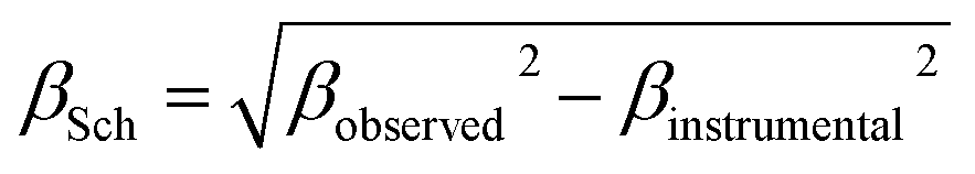
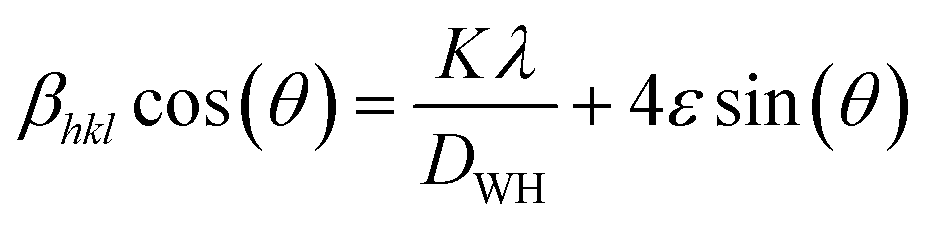
XRD can be used to assess the peak broadening, which provides insights into the crystallite size and lattice strain caused by dislocations. The mean crystallite size of KSC was determined using various methods, including Scherrer's formula, Williamson–Hall method (WeH), and SEM analysis. Scherrer's formula (DSch) is given by:25
 | (3) |
 | (4) |
|
β = 4εtan(θ)
| (5) |
 | (6) |
A plot was generated with βhklcos(θ) on the y-axis and 4εsin(θ) on the x-axis for the prepared sample as shown in Fig. 3. The crystalline size DWH was calculated from the y-intercept, while the strain ε was derived from the slope of the linear regression of the data. The crystallite size and strain values estimated using Scherrer's method and the Williamson–Hall (WH) method are presented in Table 1† (see the ESI for details). From these values, it is evident that the crystallite size calculated using the Williamson–Hall method is larger than the size obtained by Scherrer's method. This discrepancy arises due to the fact that the Williamson–Hall method includes strain-induced broadening, while Scherrer's method assumes that all peak broadening is due to crystallite size alone. Therefore, the broader diffraction peaks observed in K2SnCl6 can be partially attributed to the presence of microstrain, which leads to an increase in the diffraction peak width, causing an overestimation of the crystallite size. The grain size observed by SEM (Fig. 4) is much larger than those calculated by the WH and Scherrer's methods (Table 1†). This can be attributed to the observation that each particle seen in the SEM image is composed of crystallized grains. The larger grain size observed in SEM suggests that the material has fewer grain boundaries, which is advantageous for energy storage applications. Reduced grain boundaries can lower resistance to ion transport, thereby enhancing ionic conductivity and mechanical stability.
 | ||
| Fig. 3 The strain graph, (the Debye–Scherrer plot for K2SnCl6 compound shown inset). | ||
 | ||
| Fig. 4 Images obtained through scanning electron microscopy SEM with size distribution histogram. | ||
The Raman spectra presented in Fig. 5 reveal further structural details, displaying three distinct bands, each corresponding to a specific vibrational mode. The initial band, the F2g mode, appears near 167 cm−1 and is associated with the in-plane bending of the Sn–Cl–Sn bonds. The second band, identified as the Eg mode, is observed around 243 cm−1 and corresponds to the asymmetric stretching of the Sn–Cl bonds. Finally, the A1g mode, which appears near 322 cm−1, is linked to the symmetric stretching of the Sn–Cl bonds.
 | ||
| Fig. 5 Raman spectrum of K2SnCl6. | ||
3.2 Impedance spectroscopy results
Complex impedance spectroscopy (CIS) is an essential and effective technique for investigating the electrical properties of a material. This, provides important insights into ion migration within the KSC, including relaxation time and electrical conductivity.27 The complex impedance method is a noninvasive technique that reveals the distinct contributions of a material's core (grain), grain boundaries, and electrodes, particularly when affected by a reversed electric field. When an alternating electric field is applied, charge carriers typically set in motion, resulting in phenomena such as dipole reorientation, charge displacement, and the formation of space charges. This dynamic process allows complex impedance analysis to effectively separate and identify the specific roles of grains, grain boundaries, and electrodes in enabling charge movement through the material.Fig. 6(a) shows the frequency-dependent real component of the complex impedance Z′(ω) versus the imaginary component Z′′(ω) at various temperatures. This graph, commonly known as the Cole–Cole plot or Nyquist diagram, typically features three distinct semicircles for any dielectric material. Each semicircle represents the individual contributions of the grain, grain boundary, and electrode-material interface to the overall impedance. The semicircles observed in the high-frequency range correspond to the grain contribution, whereas those in the low-frequency region reflect the influence of the grain boundary. Finally, the semicircles in the ultralow-frequency range are attributed to the electrode-material interface.28 The graph reveals a clear semicircular arc in the Nyquist plot of the sample, with the center of the arc positioned below the real impedance axis. This suggests the absence of Debye-type behavior. According to Debye's model, materials exhibiting a single relaxation time should produce an ideal semicircle with the center lying along the real axis. The appearance of a single semicircular arc indicates that the electrical properties of the sample were dominated by grains (bulk). This further highlights the lack of electrode polarization and confinement of the relaxation process to the bulk of the crystal. The impedance spectra at all temperatures were analyzed and fitted using the ZView Lab software. For this purpose, an appropriate circuit model was derived by a parallel combination of resistance, capacitance, and fractal capacitance, as shown in the inset of Fig. 6(a).
 | ||
| Fig. 6 Nyquist plots (Z′′ vs. Z′) for K2SnCl6 compound at various temperatures (a) and (b) the variation of Rg with temperatures. | ||
Fig. 6(a) further illustrates that as the temperature increases, the diameter of the semicircle specifically the intersection on the real axis decreases noticeably. This reduction signifies an increase in DC conductivity with rising temperatures. Moreover, it confirms the thermally activated conduction process and highlights the semiconducting characteristics of the compound. The values of the optimized parameters, extracted from the equivalent circuit model are summarized in Table 3† (ESI). The variation in Rg with temperature is shown in Fig. 6(b).
The temperature-dependent variation of Z′(ω) in KSC is shown in Fig. 7(a), revealing a sigmoidal pattern with increasing temperature. At lower frequencies, Z′(ω) exhibited higher magnitudes, which progressively decreased with increasing frequency and temperature. This trend aligns with the characteristics of a negative temperature coefficient of resistance (NTCR), where the resistance diminishes with increasing in temperature. No noticeable change in Z′(ω) was noted with temperature in the high-frequency region, causing the values to converge, which can likely be attributed to the accumulation of space charges accompanied by a decrease in the barrier properties, which in turn boosts the alternating current (ac) conductivity.29
 | ||
| Fig. 7 Frequency dependence of (a) the real part (Z′) and (b) the imaginary part (Z′′) of the impedance at various temperatures. | ||
The variation of the imaginary component of the impedance Z′′(ω) as a function of frequency can be interpreted as a loss spectrum. This fluctuation reveals a distinct relaxation peak that is notably influenced by temperature, as illustrated in Fig. 7(b). Essentially, these relaxation peaks appear when the frequency of the external field resonates with the frequency of the localized electron hopping. Interestingly, the relaxation peaks observed are significantly broader than the ideal Debye curve, suggesting that KSC exhibits a non-Debye-type relaxation behavior. The span of the peak is directly related to the relaxation time, and this width clearly increases as the temperature increases. As the temperature increased, the relaxation peak gradually expanded.
The electrical conductivity can be derived from the following equation:
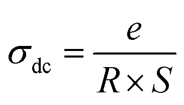 | (7) |
 | (8) |
 | ||
| Fig. 8 Variation of dc conductivity (ln(σdc × T)) as a function of (1000/T). | ||
3.3 Study of electrical conductivity
The electrical conductivity of disordered solids arises from the thermally activated motion of charge carriers, which undergo a hopping process when subjected to an electric field.Fig. 9 shows the variation in temperature-dependent AC conductivity as a function of frequency. The conductivity observed in the low-frequency region was attributed to DC conductivity, whereas that in the high-frequency range was driven primarily by AC conductivity. The presence of both frequency-independent and temperature-dependent DC conductivities resulted in flattening of the conductivity curves at lower frequencies. However, as the frequency increased, the curves expanded significantly, indicating a significant frequency dispersion, mainly resulting from the effect of AC conductivity.
 | ||
| Fig. 9 Electrical conductivity spectra of the studied system at various temperatures. | ||
Frequency-independent DC conductivity and frequency-dependent AC conductivity noted are explained using the jump-relaxation model (JRM) proposed by Funke. According to this model, in the low-frequency range, ions can effectively hop to adjacent sites, with these successful transitions facilitated by the prolonged availability of sites, thereby driving the long-range translational motion of ions that contribute to DC conductivity. By contrast, in the high-frequency range, both successful and unsuccessful hops occur. In the case of unsuccessful hopping, the ion may return to its original position, resulting in back-and-forth motion. On the other hand, during a successful hop, the ion moves to a new site and becomes stable there, whereas the surrounding ions relax in response. As the frequency increases, the proportion of successful hops relative to unsuccessful ones grows, which accounts for the dispersive nature of conductivity observed in the high-frequency range.30 To analyze the AC conductivity of semiconductors, Jonscher's universal power law provides an excellent framework, that accurately describes the behavior of these materials. The frequency and temperature dependence of AC conductivity can be effectively described using this universal power law:31
| σac(ω, T) = σdc(T) + AωS | (9) |
 | (10) |
 | ||
| Fig. 10 (a) The temperature dependence of the frequency exponent s, (b): evolution of (1 − s) against the temperature and the deduced W(I)M and W(II)M energies for the CBH mechanism. | ||
Curve fitting is used to determine the value of Wm, which is approximately (0.21–0.41) eV, as shown in eqn (10) and illustrated in Fig. 10(b). In accordance with the CBH mode, the equation for AC conductivity is as follows:39
 | (11) |
 | (12) |
Fig. 11 illustrates the temperature dependence of ln(σAC) at various frequencies. The experimental data were effectively fitted using the theoretical conductivity equation (eqn (11)), yielding results that closely align with the observed values. The specific parameters determined for the CBH model are illustrated in Table 4† (ESI).
 | ||
| Fig. 11 Variation of AC conductivity versus 1000/T for CBH model. | ||
A qualitative analysis of the data, revealed that the number of localized states increased as the frequency rose. This increase can be attributed to a reduction in disorder, which enhances the charge transport. Fig. 12 illustrates the relationship between hopping distance (Rω), temperature, and frequency. As the frequency increases, Rω decreases, demonstrating an inverse trend between these variables. In contrast, Rω increases with rising temperature, driven by the thermal energy enhancing the hopping process. At lower temperatures, Rω remains stable, showing minimal sensitivity to temperature changes. Notably, the observed hopping distances are within the range of the K–Cl interatomic spacing (3.269 Å). This close agreement suggests that the charge transport mechanism in K2SnCl6 is strongly influenced by its local structural environment, particularly the arrangement of potassium (K) and chlorine (Cl) ions within the cubic perovskite lattice. The similarity between the hopping distances and the K–Cl bond length further supports the correlated barrier hopping (CBH) model as the dominant charge-transport mechanism, where charge carriers overcome energy barriers between adjacent sites in a thermally activated manner. This finding underscores the crucial role of crystal structure in determining electrical properties and offers valuable insights for designing materials with enhanced ionic conductivity for energy storage applications.40
 | ||
| Fig. 12 The temperature dependence of Rω (Å) of K2SnCl6 at different indicated frequencies. | ||
Additionally, the analysis highlights that higher frequencies correspond to shorter hopping distances, further reinforcing the inverse relationship between frequency and Rω. These trends reflect the interplay between frequency, temperature, and hopping dynamics.
In ionic architectures, the polarization of the network is intrinsically linked to the presence of ionic carriers. These carriers manifest as entities, termed polarons. Within the effective mass approximation framework, an electron traversing a deformable or polarizable medium engenders categories of large or small polarons. A large polaron's wave function, accompanied by associated lattice deformations, spans multiple lattice sites. However, in a flawless lattice, absolute self-trapping remains elusive. Given the finite vibrational frequencies of phonons, ionic polarization can adapt to the motion of polaron but only if its progression is sufficiently gradual. Consequently, large polarons, characterized by diminished kinetic energy, traverse the lattice in a manner akin to that of free electrons, albeit with an augmented effective mass.
Conversely, when the distortion induced by a charge carrier is confined to its immediate neighboring ions, a small polaron emerges. In this scenario, conductivity is heavily influenced by the carrier's interaction with this distortion, leading to a relatively low mobility that is acutely sensitive to temperature changes.
3.4 Analysis of the electric modulus
To gain insight into the relaxation process in KSC, a comprehensive analysis of the complex modulus spectra was conducted. The complex electric modulus, introduced by Macedo et al.,41 is defined as the inverse of the complex permittivity. This approach is particularly effective for studying electrical relaxation processes related to space charge distribution, as it minimizes the influence of electrode effects. The electric modulus characterizes the relaxation behavior of the electric field within the material under conditions of constant dielectric displacement. It is mathematically expressed as follows:
 | (13) |
 | (14) |
 | ||
| Fig. 13 Evolution of the imaginary part M′′ of the electric modulus as a function of frequency at different temperatures. | ||
The frequency at which M′′ reaches its maximum value is referred to as fmax and the maximum value of M′′ is denoted as  . The two parameters, “a” and “b,” control the shape of the low-frequency and high-frequency sides, correspondingly. Additionally, the smoothing parameter is represented by “c.” When both “a” and “b” are set to 1, and “c” is set to 0, a modified KWW function that fits the data well is obtained, as shown in Fig. 13. The associated parameter values are listed in Table 5† (ESI). The data suggest that as the temperature increases, both the “a” and “b” values also rise, indicating that M′′ increasingly approximates ideal Debye-type behavior at higher temperatures. The relaxation time is determined using the following equation:
 | (15) |
The mean activation energy of the charge carriers is calculated using the Arrhenius formula, as demonstrated below:
 | (16) |
The activation energy can be calculated by analyzing the plot of ln(τ) versus 1000/T, as depicted in Fig. 14. From this analysis, the activation energy is determined to be 0.197 ± 0.07 eV. Under these circumstances, owing to the presence of a single peak, neither the relaxation frequencies nor the peak maxima are useful for determining actual microstructures. There is still some uncertainty regarding whether the observed peak can be attributed to the grain or to other components. One of the most effective approaches to clarify this ambiguity is to combine the spectroscopic displays of M′′ and Z′′. This method provides more detailed information than individual separation. Thus, the spectra of M′′ and Z′′, normalized for the current devices, can be displayed at an arbitrary temperature of 350 K, as shown in Fig. 15. This figure demonstrates that the electrical modulus and impedance data peaks occur at two distinct frequencies.43 Overall, if the peaks of Z′′ and M′′ occur at different frequencies, the process is considered to be short-range. However, in the long-range scenario, the charge carrier peaks occur at the same frequency. In this material, the mismatch between the two peaks at various temperatures suggests the presence of short-range movement of charge carriers.44
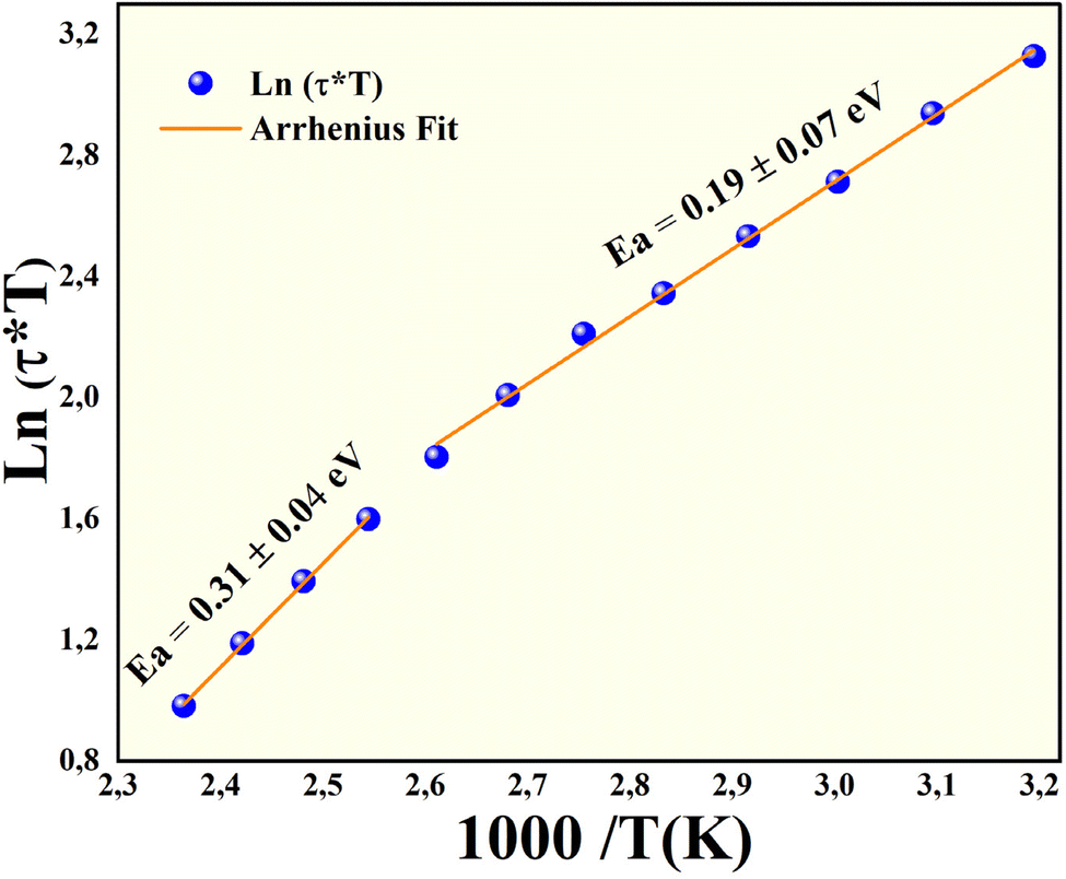 | ||
| Fig. 14 Variation of ln(τxT) as a function of 1000/T for the K2SnCl6 compound. | ||
 | ||
| Fig. 15 Variation of Z′′ and M′′ with frequency at (393 K and 423 K) temperature of K2SnCl6 perovskite. | ||
4 Conclusions
Potassium tin chloride (K2SnCl6, KSC) was successfully synthesized via an ambient-temperature antisolvent method, yielding a cubic perovskite structure (lattice parameter a = 10.00 ± 0.04 Å, volume V = 1001.66 ± 0.01 Å3) with high crystallinity, as confirmed by X-ray diffraction, Raman spectroscopy, and electron microscopy. SEM analysis revealed that the grain size was significantly larger than the crystallite size, with an average grain size of 10.03 ± 0.08 μm. The material exhibited structural stability with a noticeable microstrain of 1.11 × 10⁻³ ± 0.01, as calculated from the Williamson–Hall method.Impedance spectroscopy revealed thermally activated ionic conductivity with a low activation energy of 0.176 ± 0.004 eV, consistent with ion-hopping conduction. Analysis of AC conductivity using Jonscher's power law indicated that correlated barrier hopping, driven by the high mobility of K+ ions, was the dominant charge transport mechanism. Electric modulus spectroscopy demonstrated non-Debye relaxation behavior, with relaxation times decreasing systematically with rising temperature, highlighting the strong temperature dependence of charge carrier dynamics.
The material exhibited ionic conductivity of 7.564 × 10⁻⁹ Ω−1 cm−1 at 423 K, coupled with its stability and straightforward synthesis, positioning KSC as a promising lead-free candidate for optoelectronic devices and energy storage systems, such as chloride-ion batteries. The findings advance the understanding of ionic conduction mechanisms in KSC, linking its cubic perovskite framework to efficient ion transport.
This study not only enhances the comprehension of ion transport in KSC but also emphasizes its potential for use in various applications. Future work should focus on optimizing ionic conductivity (e.g., through doping or defect engineering) and evaluating the material's performance in prototype solid-state devices, to bridge laboratory-scale findings with practical applications.
Data availability
Data will be shared upon reasonable request to the corresponding author.Author contributions
S. Nasri: conceptualization, methodology, investigation, data analysis, and writing, original draft. A. Jraba: formal analysis, data curation, and review of the manuscript. I. Garaoui: synthesis of materials, experimental work, and data interpretation. A. Oueslati: supervision, funding acquisition, and project administration. E. Elaloui: writing, review and editing, validation, and visualization.Conflicts of interest
The authors declare that they have no known competing financial interests or personal relationships that could have appeared to influence the work reported in this paper.Acknowledgements
We would like to express our sincere gratitude to the High Minister of Scientific Research of Tunisia for their support and encouragement throughout the course of this research.References
- I. Romdhane, A. Ajmi, M. B. Bechir, R. Barilleb and A. Ben Rhaiem, Cs2ZnCl4: a lead-free all-inorganic perovskite with a large dielectric permittivity, RSC Adv., 2024, 14, 36253, 10.1039/d4ra04755a
.
- R. Kalthoum, M. B. Bechir, A. B. Rhaiem and M. H. Dhaou, Opt. Mater., 2022, 125, 112084 CrossRef CAS
- F. Deschler, M. Price, S. Pathak, L. E. Klintberg, D. D. Jarausch, R. Higler, S. Hüttner, T. Leijtens, S. D. Stranks and H. J. Snaith, et al., J. Phys. Chem. Lett., 2014, 5, 1421 CrossRef CAS PubMed
- Z. K. Tan, R. S. Moghaddam, M. L. Lai, P. Docampo, R. Higler, F. Deschler, M. Price, A. Sadhanala, L. M. Pazos and D. Credgington, et al., Nat. Nanotechnol., 2014, 9, 1 CrossRef PubMed
- K. Xiao, R. Lin, Q. Han, Y. Hou, Z. Qin, H. T. Nguyen, J. Wen, M. Wei, V. Yeddu, M. I. Saidaminov, Y. Gao, X. Luo, Y. Wang, H. Gao, C. Zhang, J. Xu, J. Zhu, E. H. Sargent and H. Tan, Nat. Energy, 2020, 5, 870–880 CrossRef CAS
- M. Ben Bechir and F. Alresheedib, Morphological, structural, optical and dielectric analysis of Cs2TiBr6 perovskite nanoparticles, RSC Adv., 2024, 14, 1634, 10.1039/d3ra06860a
- I. Romdhane, A. Ajmi, M. B. Bechir, R. Barilleb and A. Ben Rhaie, Cs2ZnCl4: a lead-free all-inorganic perovskite with a large dielectric permittivity, RSC Adv., 2024, 14, 36253–36263, 10.1039/D4RA04755A
- G. Niu, X. Guo and L. Wang, Review of Recent Progress in Chemical Stability of Perovskite Solar Cells, J. Mater. Chem. A, 2015, 3(17), 8970–8980, 10.1039/C4TA04994B
- I. C. Smith, E. T. Hoke and D. Solis-Ibarra, A Layered Hybrid Perovskite Solar-Cell Absorber with Enhanced Moisture Stability, Angew. Chem. Int. Ed., 2014, 53(42), 11232–11235, DOI:10.1002/anie.201406466
- F. Giustino and H. J. Snaith, Toward Lead-Free Perovskite Solar Cells, ACS Energy Lett., 2016, 1(6), 1233–1240, DOI:10.1021/acsenergylett.6b00499
- W. Ke, C. C. Stoumpos and M. G. Kanatzidis, Unleaded Perovskites: Status Quo and Future Prospects of Tin-Based Perovskite Solar Cells, Adv. Mater., 2018, 1803230, DOI:10.1002/adma.201803230
- I. L. Braly, D. W. deQilettes, L. M. Pazos-Outon, S. Burke, M. E. Ziffer, D. S. Ginger and H. W. Hillhouse, Nat. Photonics, 2018, 12, 355–361 CrossRef CAS
- M. M. Lee, J. Teuscher, T. Miyasaka, T. N. Murakami and H. J. Snaith, Science, 2012, 338, 643–647 CrossRef CAS PubMed
- R. T. Yadlapalli, R. R. Alla, R. Kandipati and A. Kotapati, Super capacitors for 195 energy storage: Progress, applications and challenges, J. Energy Storage, 2022, 196(49), 104194, DOI:10.1016/j.est.2022.104194
- Z. Tan, J. Li, C. Zhang, Z. Li, Q. Hu, Z. Xiao, T. Kamiya, H. Hosono, G. Niu, E. Lifshitz, Y. Cheng and J. Tang, Highly Efficient Blue-Emitting Bi-Doped Cs2SnCl6 Perovskite Variant: Photoluminescence Induced by Impurity Doping, Adv. Funct. Mater., 2018, 28, 1801131, DOI:10.1002/adfm.201801131
- Z. Tan, J. Li, C. Zhang, Z. Li, Q. Hu, Z. Xiao, T. Kamiya, H. Hosono, G. Niu and E. Lifshitz, et al., Highly Efficient Blue-emitting Bi-doped Cs2SnCl6 Perovskite Variant: Photoluminescence Induced by Impurity Doping, Adv. Funct. Mater., 2018, 28, 1801131 CrossRef
- M. Lyu, J.-H. Yun and P. Chen, Addressing Toxicity of Lead: Progress and Applications of Low-Toxic Metal Halide Perovskites and Their Derivatives, Adv. Energy Mater., 2017, 7(15), 1602512, DOI:10.1002/aenm.201602512
- M. H. Futscher and J. V. Milic, Mixed Conductivity of Hybrid Halide Perovskites: Emerging Opportunities and Challenges, Front. Energy Res., 2021, 9, 629074, DOI:10.3389/fenrg.2021.629074
- S. F. Solari, S. Kumar, J. Jagielski, N. M. Kubo, F. Krumeich and C. J. Shih, Ligand-assisted solid phase synthesis of mixed-halide perovskite nanocrystals for color-pure and efficient electroluminescence, J. Mater. Chem. C, 2021, 9, 5771–5778, 10.1039/D0TC04667A
- Y. Zhang, Z. Huang, H. Gao, Z. Xu, W. Fang, Y. Chen, Y. Hu, Z. Yi, J. Huang and H. Zhu, Green anti-solvent engineering for high-efficiency and environmentally friendly perovskite solar cells, RSC Adv., 2024, 14, 1–19, 10.1039/D4RA05082G
- J. A. Lerbscher and J. Trotter, Potassium hexachlorostannate(IV) and ammonium hexachlorostannate(IV), Acta Crystallogr., 1976, 32, 2671, DOI:10.1107/S0567740876008480
- C. J. Bartel, C. Sutton, B. R. Goldsmith, R. Ouyang, C. B. Musgrave, L. M. Ghiringhelli and M. Scheffler, New tolerance factor to predict the stability of perovskite oxides and halides, Sci. Adv., 2019, 5(2), eaav0693, DOI:10.1126/sciadv.aav0693
- S. Znaidia and B. B. Mohamed, Investigation of optical, dielectric, and charge transfer properties in lead-free double perovskite Cs2MSbBr6 (M = Cu, Ag), Ionics, 2024, 30, 1177–1195, DOI:10.1007/s11581-023-05300-8
- C. Li, X. Lu, W. Ding, L. Feng, Y. Gao and Z. Guo, Formability of ABX3 (X = F, Cl, Br, I) halide perovskites, Acta Crystallogr. B, 2008, 64(Pt 6), 702–707, DOI:10.1107/S0108768108032734
- Ch. Rayssi, S. El. Kossi, J. Dhahri and K. Khirouni, Colossal dielectric constant and non-debye type re Ca0.85Er0.1Ti1-x Co4x/3O3 (x¼0.15 and 0.2) ceramic, J. Alloys Compd., 2018, 759, 93e99, DOI:10.1016/j.jallcom.2018.05.155
- G. K. Williamson and W. H. Hall, X-ray line broadening from filed aluminium and wolfram, Acta Metall., 1953, 1, 22–31, DOI:10.1016/0001-6160(53)90006-6
- P. Sengupta, P. Sadhukhan, A. Ray, R. Ray, S. Bhattacharyya and S. Das, Temperature and frequency dependent dielectric response of C3H7NH3PbI3 : A new hybrid perovskite, Appl. Phys., 2020, 127, 204103, DOI:10.1063/1.5142810
- A. Ray, A. Roy, S. Bhattacharjee, S. Jana, C. K. Ghosh, C. Sinha and S. Das, Correlation between the dielectric and electrochemical properties of TiO2-V2O5 nanocomposite for energy storage application, Electrochim. Acta, 2018, 266, 404 CrossRef CAS
- D. K. Pradhan, P. Misra, V. S. Puli, S. Sahoo, D. K. Pradhan and R. S. Katiyar, Studies on structural, dielectric, and transport properties of Ni0. 65Zn0. 35Fe2O4J, Appl. Phys., 2014, 115, 243904, DOI:10.1063/1.4885420
- K. Agrawal, B. Behera, S. C. Sahoo, S. K. Rout, A. Kumar, D. K. Pradhan and P. R. Das, Electrical conduction mechanism in multiferroic Gd doped GaFeO3, Chem. Phys. Impact., 2023, 7, 100358, DOI:10.1016/j.chphi.2023.100358
- A. K. Jonscher, The universal’ dielectric response, Nature, 1977, 267, 673–679 CrossRef CAS
- S. Nasri, M. Megdiche and M. Gargouri, DC conductivity and study of AC electrical conduction mechanisms by non-overlapping small polaron tunneling model in LiFeP2O7 ceramic, Ceram. Int., 2016, 42, 943–951, DOI:10.1016/j.ceramint.2015.09.023
- Y. B. Taher, A. Queslati, K. Khirouni and M. Gargouri, Impedance spectroscopy and conduction mechanism of LiAlP2O7 material, Mater. Res. Bull., 2016, 78, 148–157, DOI:10.1016/j.materresbull.2016.02.033
- A. Ghosh, Transport properties of vanadium germanate glassy semiconductors, Phys. Rev. B:Condens. Matter Mater. Phys., 1990, 42, 5665–5676, DOI:10.1103/PhysRevB.42.5665
- S. Mohlah, K. K. Som, K. Bose and B. K. Chaudhuri, ac conductivity in Bi4Sr3Ca3CuyOx and Bi4Sr3Ca3−zLizCu4Ox (z=0.1-1.0) semiconducting oxide glasses, J. Appl. Phys., 1993, 74, 931–937, DOI:10.1063/1.355328
- A. Ghosh, Frequency-dependent conductivity in bismuth-vanadate glassy semiconductors, Phys. Rev. B:Condens. Matter Mater. Phys., 1990, 41, 1479–1488, DOI:10.1103/PhysRevB.41.1479
- R. Meena and R. S. Dhaka, Structural properties, dielectric relaxation and impedance spectroscopy of NASICON type Na3+xZr2−xPrxSi2PO12 ceramics, J. Am. Ceram. Soc., 2024 DOI:10.48550/arXiv.2405.11460
- S. Nasri, M. Megdiche and M. Gargouri, Electrical conduction and dielectric properties of a newly synthesized single phase: Ag0. 4Na0. 6FeP2O7, Physica B: Condensed Matter, 2014, 451, 120–127, DOI:10.1016/j.physb.2014.06.036
- A. Zolanvari, N. Goyal and S. K. Tripathi, Electrical properties of a-GexSe100-x, Pramana – J. Phys., 2004, 63, 617–625, DOI:10.1007/BF0270448
- M. B. Bechir and M. H. Dhaou, Lead-free double perovskite Cs2MBiCl6 (M = Ag, Cu): insights into the optical, dielectric, and charge transfer properties, RSC Adv., 2023, 13, 17750, 10.1039/d3ra02731g
- P. B. Macedo, C. T. Moynihan and R. Bose, The Role of Ionic Diffusion in Polarization in Vitreous Ionic Conductors, Phys. Chem. Glasses, 1972, 13(6), 171–179 CAS
- M. B. Bechir, A. Almeshal and M. H. Dhaou, Dielectric properties and charge transfer mechanism of Li1+xAlxTi2−x(PO4)3 ceramic electrolyte used in lithium batteries, Ionics, 2022, 28, 5361–5376 CrossRef CAS
- I. Ahmad, M. J. Akhtar, R. T. A. Khan and M. M. Hasan, J. Appl. Phys., 2013, 1141, 10, DOI:10.1063/1.4813782
- D. K. Pradhan, R. N. P. Choudhary, C. Rinaldi and R. S. Katiyar, Effect of Mn substitution on electrical and magnetic properties of Bi0.9La0.1FeO3, J. Appl. Phys., 2009, 106, 024102 CrossRef
Footnote |
| † Electronic supplementary information (ESI) available. See DOI: https://doi.org/10.1039/d5ra00090d |
| This journal is © The Royal Society of Chemistry 2025 |