
 Open Access Article
 This Open Access Article is licensed under a Creative Commons Attribution-Non Commercial 3.0 Unported Licence
Photoelectrochemical water splitting with In2O3−x nanofilm/black Ti–Si–O composite photoanode
Jianing Cuia,
Dongyan Ding *a,
Shengzhe Yuea and
Zhi Chenb
*a,
Shengzhe Yuea and
Zhi Chenb
aSJTU-Zhongmu Joint Research Center for Materials and Technology of Intelligent and Connected Vehicles, Institute of Electronic Materials and Technology, School of Materials Science and Engineering, Shanghai Jiao Tong University, Shanghai 200240, China. E-mail: dyding@sjtu.edu.cn
bDepartment of Electrical & Computer Engineering, Center for Nanoscale Science & Engineering, University of Kentucky, Lexington, Kentucky 40506, USA
First published on 14th February 2025
Abstract
Fabricating TiO2 with heterostructures is one of the important ways to enhance its photocatalytic activity. In this work, we fabricated black Si-doped TiO2 nanotubes (Ti–Si–O) through anodization and Sn reduction, and constructed In2O3−x nanofilm/black Ti–Si–O composite photoanode through electrochemical deposition and Ar annealing. The composition evolution, morphology, optical properties and photoelectrochemical performance of the composite photoanode were investigated. The In2O3−x/black Ti–Si–O composite photoanode exhibited excellent PEC hydrogen production performance, with a high photocurrent density of 3.76 mA cm−2 at 0 V Ag/AgCl, which was 2.16 times that of the black Ti–Si–O photoanode. The synergistic effects of Si doping, Ti3+/O vacancies and the modification with In2O3−x nanofilms provide a beneficial approach to design of high-efficiency photoanodes.
1. Introduction
With the continuous growth of global energy demand and the increasing severity of environmental issues, the development of sustainable and clean energy technologies has become an urgent priority. Photoelectrochemical (PEC) water splitting, as an efficient method for directly converting solar energy into chemical energy, has rapidly emerged in the field of advanced energy materials in recent years. PEC water splitting not only utilizes solar energy to produce clean hydrogen gas but also provides new avenues for addressing energy crises and environmental pollution.In the research on PEC water splitting, the development of efficient and stable photocatalysts is crucial. In recent years, researchers have made significant progress in this field, reporting a variety of novel catalysts1–4 and structural designs5–7 that have significantly improved the efficiency and stability of PEC water splitting. As an emerging direction in the field of advanced energy materials, PEC water splitting is continuously achieving new breakthroughs. In the future, with in-depth research and the maturation of technology, PEC water splitting is expected to play an important role in sustainable energy supply.8
In 1972 Fujishima and Honda achieved visible light-driven photocatalytic overall water splitting on the surface of titanium dioxide (TiO2), providing an example for the non-biological conversion path of solar energy.9 Since then TiO2-based semiconductor photocatalytic water splitting technology has attracted great attention.10–13 However, its wide band gap results in low utilization rate of visible light in sunlight. And at the same time, the high recombination rate of photogenerated electrons and holes limits its use in the field of photocatalysis.14–16 Currently, researchers are employing various methods to enhance the photocatalytic efficiency of TiO2, such as doping with metal17,18 or non-metal19–21 elements and coupling with narrow-bandgap semiconductors.22–24
Doping with either metal or non-metal elements can also narrow the band gap of TiO2 and broaden its light absorption range. Chen et al.25 prepared N-doped TiO2 photoanodes by annealing TiO2 photoelectrodes in an ammonia atmosphere. They found that N-doping significantly enhanced the light absorption range and charge transport capability of the TiO2 photoanodes. Si26–29 has attracted significant attention due to its abundance, low cost, and non-toxicity. After doping with Si, Ti–Si–O bonds are formed in the TiO2 lattice, which facilitates the acceleration of photogenerated charge carrier transfer and enhances photocatalytic activity. There have been reports that self-doping with oxygen vacancies can regulate some physicochemical properties of TiO2, such as light absorption, photocatalytic reaction activity and selectivity.30–32
Semiconductor heterojunction construction can effectively enhance the efficiency of hydrogen production from water splitting using TiO2. Due to excellent light and structural stability as well as good resistance to photocorrosion, In2O3 is an n-type indirect semiconductor with conduction and valence band positions that can perfectly match with TiO2.33–35 The construction of In2O3/TiO2 heterojunctions can effectively promote the separation of photoexcited electron–hole pairs, thereby enhancing the photoelectrocatalytic performance of TiO2.36,37 In2O3 can be prepared by electro-deposition of In(OH)3 followed by annealing.38 Introducing oxygen vacancies in In2O3 can narrow the band gap and enhance the absorption capacity for visible light. And the oxygen vacancies, acting as donor levels, can further improve the conductivity of In2O3.39,40 Although previous studies have enhanced the photoelectrochemical performance of TiO2 through methods such as Si doping, oxygen vacancy self-doping and In2O3 decoration, research that integrates these methods into TiO2-based systems for efficient photoelectrochemical water splitting is still limited. This study aims to integrate these methods to further improve the performance of TiO2-based photoanodes, providing new solutions for solar-driven water splitting.
Therefore, in this work, we employed Sn reduction method to prepare reduced Ti–Si–O nanotube photoanode with oxygen vacancies in the Ti–Si–O nanotubes. Furthermore, In2O3−x nanofilm was electrodeposited to modify the reduced Ti–Si–O photoanode, forming a heterojunction structure. The deposition voltage was altered to adjust the deposition rate and morphology of the indium oxide, and the influence of the deposition voltage on the PEC performance of the composite photoanode was investigated. It was found that the modification with In2O3−x nanofilm could significantly enhance the photoelectrochemical performance of Si-doped TiO2, offering new way for the design of novel TiO2-based photoanodes.
2. Experimental section
2.1. Preparation of black Ti–Si–O nanotube arrays
The fabrication process of the composite photoanode is shown in Fig. 1. First, the Ti–Si alloy (with 5 wt% Si content) prepared by vacuum arc melting was cut into sheets with dimensions of 20 mm × 10 mm × 1 mm, homogenized at 800 °C for 2 hours then cooled to room temperature with the furnace. The samples were mechanically polished with aluminum oxide. They were then ultrasonically cleaned with acetone and ethanol for 10 and 20 minutes, respectively. Anodization was carried out for 20 minutes at a voltage of 40 V using an electrolyte containing 1 wt% NH4F and 3 wt% H2O in ethylene glycol, followed by annealing at 600 °C for 2 hours to prepare Ti–Si–O nanotubes. The annealed Ti–Si–O samples and 5 g of tin particles were placed in two crucibles inside a furnace filled with argon. The reduction temperature was set at 700 °C for a duration of 4 hours. | ||
| Fig. 1 Schematic diagram of the preparation process for In2O3−x/black Ti–Si–O composite photoanode. | ||
2.2. Fabrication of In2O3−x/black Ti–Si–O composite photoanode
Nano In2O3 films were grown on the black Ti–Si–O nanotube array by using an electro-deposition and annealing method. A CHI660C workstation was employed as the power supply, with the black Ti–Si–O nanotube array serving as the working electrode, a platinum sheet as the counter electrode, and Ag/AgCl as the reference electrode in a three-electrode system to deposit indium oxide. In(OH)3 nanofilm was deposited onto the black Ti–Si–O nanotubes in 0.02 M In(NO3)3·4.5H2O solution at a bath temperature of 85 °C, with different deposition potentials of −1 V, −2 V, and −3 V for 200 seconds. The as-prepared In(OH)3/black Ti–Si–O was annealed in a tubular furnace filled with Ar at 500 °C for 2 hours to fabricate the In2O3−x/black Ti–Si–O composite photoanode.2.3. Materials characterization and PEC measurement
The morphology of the samples was examined using a scanning electron microscope (SEM, RISE-MAGNA, TESCAN, CZ). The chemical composition was analyzed with an energy-dispersive spectrometer (EDS, INCA X-ACT, Oxford, UK). The crystal structure were characterized with X-ray diffractometer (XRD, D8 ADVANCE Da Vinci, Bruker, Germany) over a 2θ range of 20° to 80°. The chemical states of the elements and the position of the valence band (VB) were measured with X-ray photoelectron spectroscopy (XPS, Axis Ultra DLD, Kratos, Japan), with the 284.5 eV C 1s peak used to calibrate the binding energies of other elements. The optical properties of different samples were evaluated using UV absorption spectrophotometer (wavelength range 250–750 nm) (PerkinElmer Inc., Lambda 950, USA).Photoeletrochemical performance of the samples in a three-electrode system was studied with 1 M KOH (PH = 13.3) as electrolyte. The photoanode, platinum plate and Ag/AgCl served as the working electrode, counter electrode and reference electrode, respectively. A 150 W Xenon lamp (Lanpu, XQ350W, China) with an intensity of 100 mW cm−2 (corresponding to AM 1.5G irradiance) was used to simulate solar irradiance. Photocurrent–voltage dependence was tested using linear sweep voltammetry (LSV) with a scan rate of 0.05 V s−1. Charge transfer dynamics between the In2O3−x deposition and the black Ti–Si–O nanotube substrate, as well as between the electrode and the electrolyte, were studied under open circuit potential (OCP) irradiation from 0.1 Hz to 105 Hz using electrochemical impedance spectroscopy (EIS). Mott–Schottky curve was tested under dark conditions at 1000 Hz. The photocurrent–time (I–t) curve was obtained under intermittent light/dark switching at 0 V vs. Ag/AgCl.
3. Results and discussions
3.1. Composition and morphology characterizations
Microstructural and XRD characterization of black Ti–Si–O (Si-doped TiO2) could be found in our previous report.40 Fig. 2 shows XRD of different photoanodes. Compared to the XRD pattern of the black Ti–Si–O photoanode, four additional peaks attributed to In2O3−x were observed, indicating that the electrodeposition and annealing process did not affect the crystal structure of the black Ti–Si–O photoanode. In the XRD pattern, four distinct diffraction peaks observed at 21.58°, 30.56°, 51.01°, and 60.82° correspond to the (211), (222), (431), and (622) crystal planes of cubic In2O3−x, respectively.39,40 The diffraction peaks in the XRD pattern of the composite photoanode were well assigned to black Ti–Si–O and In2O3. The composite photoanode is composed of In2O3−x and black Ti–Si–O. Moreover, the XRD pattern of the composite photoanode after prolonged light illumination shows no significant changes, indicating that the composite photoanode possesses excellent structural stability. | ||
| Fig. 2 XRD patterns of the different samples. | ||
Fig. 3 shows SEM images of In2O3−x nanofilms deposited on black Ti–Si–O nanotubes for different deposition voltages. The black Ti–Si–O nanotubes had an average diameter of 68 nm and a length less than 1 μm. It can be observed that as the deposition voltage increased, the amount of deposited In2O3 gradually increased. For a deposition voltage of −1 V, In2O3−x exhibited an irregular nanosheet-like structure. The thickness of In2O3−x nanosheets was approximately tens of nanometers, uniformly covering the surface of the black Ti–Si–O photoanode. As the voltage increased, the deposition rate also increased and easily grew up as a dense film attached to the black Ti–Si–O nanotubes. The composite photoanode obtained at a deposition voltage of −1 V had a larger specific surface area in comparison with the other two composite photoanodes. Fig. 3g shows the morphology of the composite photoanode after 1 hour of light illumination. Compared with the photoanode that has not undergone electrochemical performance testing, no significant changes have occurred. This indicates that the composite photoanode has good stability.
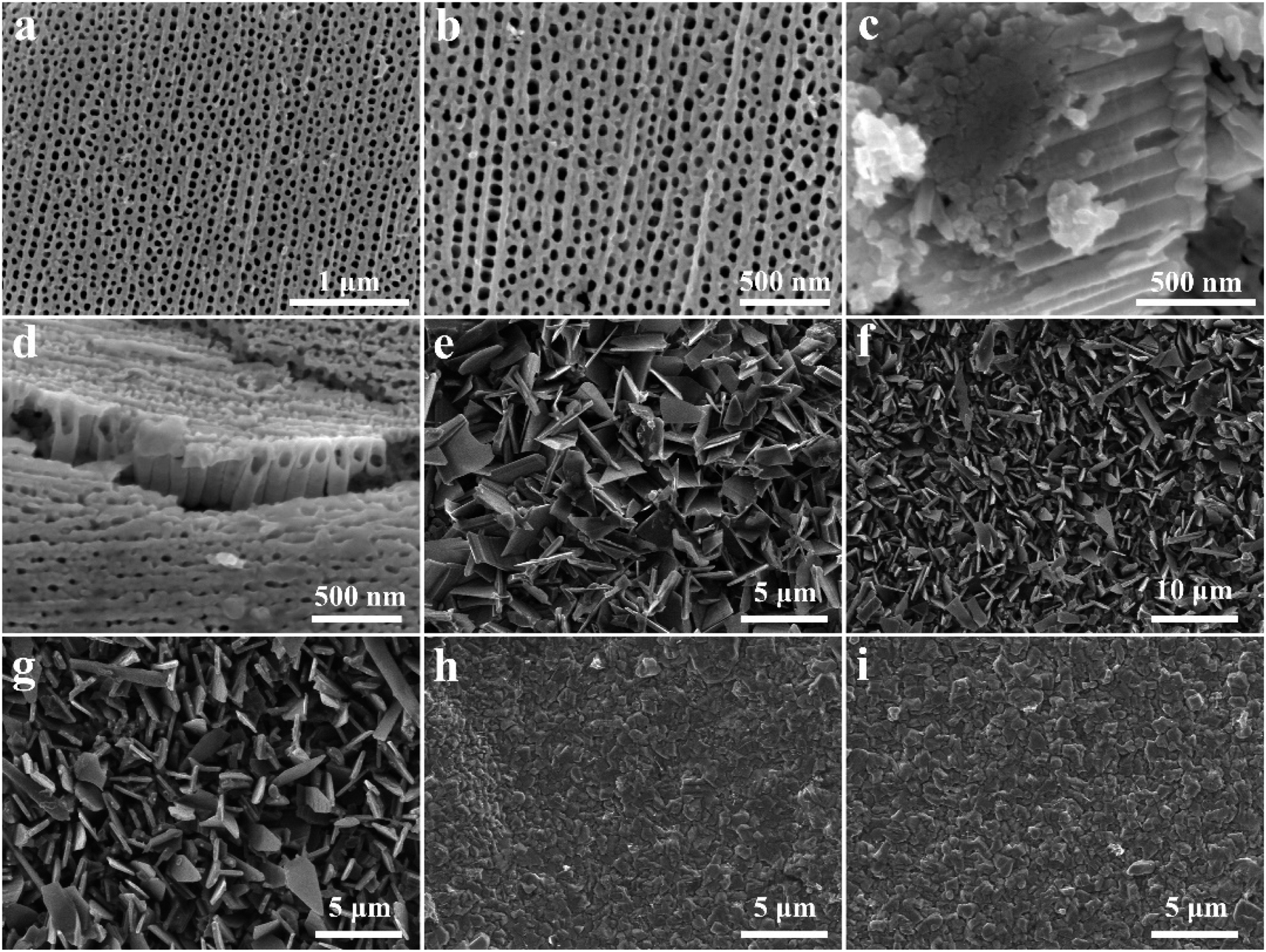 | ||
| Fig. 3 SEM images of the (a and b) surface of black Ti–Si–O photoanode, (c and d) scratched surface of the black TiSiO photoanode, (e) surface of the −1 V In2O3−x/black Ti–Si–O photoanode, (f and g) surface of the −1 V In2O3−x/black Ti–Si–O photoanode after 1 hour of testing, (h and i) surfaces of the −2 V and −3 V In2O3−x/black Ti–Si–O photoanodes. | ||
The EDS spectrum of −1 V In2O3−x/black Ti–Si–O is shown in Fig. 4. In the composite photoanode, Ti, Si, and O elements were found and they were in the black Ti–Si–O nanotubes. The In element was also evenly distributed on the surface of the composite photoanode. The nanofilm is composed of In2O3. Obviously, a composite heterojunction system composed of a nanofilm and black nanotubes was successfully prepared.
 | ||
| Fig. 4 EDS elemental mapping results of the surface of −1 V In2O3/black Ti–Si–O composite photoanode. (a) SEM image of the surface, (b–e) elemental mapping of Ti, Si, O and In element, respectively. | ||
Further analysis of the chemical status of the elements in the heterojunction was performed using XPS. As shown in Fig. 5. Ti, Si, O, and In elements were detected in the full spectrum of XPS (Fig. 5a). The spectrum of Ti is shown in Fig. 5b, where the two peaks of the Ti element spectrum located near 458.6 eV and 464.4 eV belong to the Ti4+–O bond,34 and the other two peaks near 457.6 eV and 463.4 eV belong to the Ti3+–O bond in the reduced Ti–Si–O.41,42 The Si 2p spectrum was found near 101.7 eV (Fig. 5c), which is slightly lower than the binding energy of Si in SiO2, indicating that the Si element did not form a SiO2 phase but entered the TiO2 lattice in the form of Ti–Si–O bonds. Four peaks were found in the O 1s spectrum (Fig. 5d), located near 529.7 eV, 530.6 eV, 529.1 eV and 531.4 eV. The first two peaks belong to the In–O bond and the oxygen vacancy peak in In2O3−x, and the latter two peaks belong to the Ti–O bond and the oxygen vacancy in the reduced Ti–Si–O. In the In 3d spectrum of Fig. 5e, the two peaks near 452.1 eV and 444.5 eV correspond to the In 3d5/2 and In 3d3/2 of In2O3−x, respectively.34 Obviously, we have successfully prepared a composite photoanode composed of In2O3−x and black Ti–Si–O.
 | ||
| Fig. 5 XPS patterns of (a) full spectra, (b) Ti 2p, (c) Si 2p, (d) O 1s and (e) In 3d of the −1 V In2O3−x/black Ti–Si–O photoanode. | ||
3.2. Optical properties
Ultraviolet-visible diffuse reflectance spectroscopy (UV-vis DRS) was utilized to study the optical properties of the prepared samples. As shown in Fig. 6, the absorption spectrum reveals the sample's capacity to absorb light. It can be observed that, compared to the bare black Ti–Si–O nanotube samples, the In2O3−x/black Ti–Si–O composite photoanode demonstrated significantly higher light absorption within the 400–700 nm range, and the absorption edge of the composite photoanode has undergone a redshift. Clearly, the modification with In2O3−x nanofilm had endowed the composite photoanode with enhanced light absorption capability. This may be attributed to the formation of heterojunction structures following the In2O3−x modification, which accelerated the separation rate of photogenerated charge carriers. Oxygen vacancies in In2O3−x, acting as defect states, could provide more active sites, and promote charge transport, and thereby further increase the carrier concentration. | ||
| Fig. 6 (a) UV-vis diffuse reflectance spectra, (b) corresponding plots of transformed Kubelka–Munk function versus the energy. | ||
Based on Fig. 6, the bandgap (Eg) values of the composite photoanode and the black Ti–Si–O photoanode were calculated using the Kubelka–Munk formula:43,44
| (αhv)n = A(hν − Eg) | (1) |
The Eg value can be obtained from the x-intercept of the plot in Fig. 6b. It was found that the bandgaps of the −1 V, −2 V, and −3 V composite photoanodes, as well as the bare black Ti–Si–O photoanode, were 2.77 eV, 2.86 eV, 2.93 eV, and 3.10 eV, respectively. Obviously, the modification with In2O3−x could narrow the bandgap of the black Ti–Si–O photoanode, significantly enhancing the light absorption capacity of the composite photoanode.
3.3. PEC performance
Fig. 7 shows the PEC water splitting characteristics of different photoanodes. It can be seen that, compared to black Ti–Si–O, the PEC water splitting characteristics of the composite photoanodes are improved after modification with In2O3−x. The −1 V In2O3−x/black Ti–Si–O photoanode exhibited the highest photocurrent density and the highest IPCE efficiency. Moreover, as the deposition voltage increased, the photocurrent density and the highest IPCE efficiency began to decrease gradually. Fig. 7a shows the I–t curves of the In2O3−x/black Ti–Si–O composite photoanode and the black photoanode at different voltages. All photoanodes exhibited a rapid response to light illumination, with a quick increase in photocurrent density when exposed to light. It can be found that the PEC performance of the In2O3−x/black Ti–Si–O photoanode is significantly better than that of the black Ti–Si–O photoanode (1.74 mA cm−2). This may be due to the better light absorption capability of In2O3−x and the promoting effect of the heterojunction on the transport of photogenerated charge carriers. The composite photoanode deposited at −1 V exhibited the highest photocurrent density (3.76 mA cm−2), which was significantly better than those of the composite photoanodes deposited at −2 V (2.96 mA cm−2) and −3 V (2.67 mA cm−2). Thus, finding the optimal deposition voltage has an important impact on the performance of the In2O3−x/black Ti–Si–O. Apparently, a deposition voltage that was too high could greatly accelerate the deposition rate of In2O3−x. The deposition voltage affects the photoelectric current performance by altering the thickness, structure, and surface coverage of the film. A higher deposition voltage increases the growth rate of the film. A thicker film can absorb more light, but it may also increase the probability of charge recombination, reducing the efficiency of the photoelectric current. On the other hand, a lower deposition voltage results in a thinner film that may absorb less light, but the charge transport path is shorter, reducing the probability of recombination. A higher deposition rate can also lead to uneven surface coverage, while a lower deposition voltage typically results in more uniform surface coverage, which helps to improve charge transport efficiency. Moreover, a lower deposition voltage can produce a purer film, reducing defects and impurities. The film formed at a deposition voltage of −1 V achieved the best balance between light absorption and charge transport, demonstrating the highest photoelectric current density. Although a higher deposition voltage could increase the thickness of the film, it could also lead to increased charge recombination, thereby reducing PEC performance.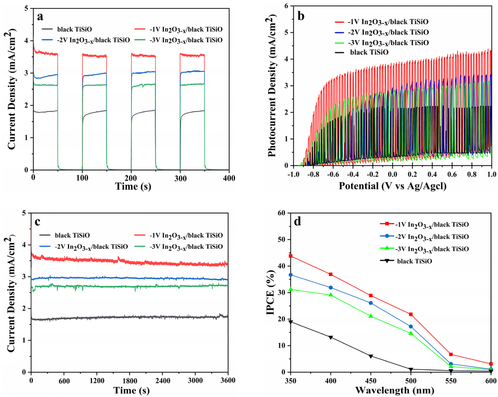 | ||
| Fig. 7 (a) Transient I–t curves of the photoanodes at different deposition voltages, (b) transient linear sweep voltammetry (LSV) curves, (c) stability of photocurrent density for different composite photoanodes (0 V vs. Ag/AgCl), (d) IPCE of different photoanodes. | ||
Fig. 7b illustrates the LSV curves of the composite photoanodes with deposition potentials of −1 V, −2 V, and −3 V and the black Ti–Si–O photoanode. All photoanodes show a prompt response to light exposure, aligning with the I–t curves depicted in Fig. 7a. At 0 V vs. Ag/AgCl, the photocurrent densities for all the composite photoanodes were recorded as 3.76 mA cm−2, 2.96 mA cm−2, and 2.67 mA cm−2, respectively. Whereas, the photocurrent density (1.74 mA cm−2) for the black Ti–Si–O photoanode was considerably lower than those of the composite photoanodes with the heterojunction of In2O3−x and the black Ti–Si–O. The −1 V In2O3−x/black Ti–Si–O photoanode exhibited superior PEC hydrogen production performance, mainly due to the moderate In2O3−x modification.
Fig. 7c shows the photocurrent densities of various photoanodes after one hour of illumination at 0 V vs. Ag/AgCl. Within the KOH electrolyte solution, all photoanodes demonstrated stable PEC performance with a minimal decrease in photocurrent density for less than 5%. This indicates that the photocurrent density of the In2O3−x/black Ti–Si–O photoanodes remains largely unchanged, signifying that the composite photoanode possessed good photoelectrochemical stability, which was consistent with previous reports.45 This long-term stability is crucial for practical PEC applications, as it ensures the reliability and efficiency of the photoanode over extended periods.46–48 This good stability should be mainly attributed to the photoelectrochemical stability of In2O3−x nanofilms coated on the black Ti–Si–O photoanode. In2O3−x exhibited good chemical stability in the electrolyte. It improved charge separation efficiency and significantly suppresses the recombination of photogenerated charge carriers, thereby greatly enhancing the photoelectrochemical water-splitting capability of the composite photoanode.
Fig. 7d shows the IPCE curves of different photoanodes. The IPCE results indicate that −1 V In2O3−x/black Ti–Si–O exhibits the highest photon conversion efficiency (43.8%). It can be seen that after the modification with In2O3−x, the photoelectrochemical quantum efficiency of the composite photoanodes was significantly enhanced. The probability of recombination of photogenerated carriers was greatly reduced, and the photocurrent density also increased accordingly.
Fig. 8a illustrates the transient open-circuit voltage (OCP) curves for various photoanodes under simulated solar illumination, which characterized the photoresponse and photoelectrochemical (PEC) performance of the In2O3−x/black Ti–Si–O photoanodes. As shown in Fig. 8a, all of the composite photoanodes with In2O3−x deposition had a negative shift relative to the black Ti–Si–O photoanode, indicating that the deposition of In2O3−x had quickened the separation velocity of photogenerated charge carriers. After the power supply turned off, photogenerated charge carriers underwent recombination, and the recombination of charges caused the open-circuit voltage (Voc) to decay. The lower the decay rate of Voc was, the slower the charge recombination kinetics was. The lifetime of photogenerated charge carriers was closely related to the decay rate of Voc. Obviously, −1 V In2O3−x/black Ti–Si–O photoanode exhibited a lower decay rate, indicating that this composite photoanode had slower recombination kinetics and a longer lifetime for photogenerated charge carriers. A slower decay rate of the open-circuit voltage typically implied that the recombination rate of photogenerated electrons and holes was slower, which enhanced their chances of participating in photocatalytic reactions, thereby improving photocatalytic efficiency. A slower decay rate may indicate a higher charge separation efficiency, which is a key factor in improving photocatalytic performance. Effective charge separation could reduce the recombination of electron–hole pairs, allowing more charge carriers to participate in photocatalytic reactions.
 | ||
| Fig. 8 (a) Transient open-circuit potential (OCP) curves of the composite photoanode at different voltages, (b) Mott–Schottky (MS) curves under light-off conditions. | ||
The Mott–Schottky (MS) plots from the graph revealed that all three composite photoanodes exhibit a positive slope, indicating that they were n-type semiconductors. According to the Mott–Schottky equation for the linear region of n-type semiconductors,49 it was possible to calculate the donor density (Nd) and the flat band potential (Vfb) for the three composite photoanodes:
| 1/C2 = (2/εε0eNDA2) (V − Vfb − kBT/e) | (2) |
The donor densities for the −1 V In2O3−x/black Ti–Si–O, −2 V In2O3−x/black Ti–Si–O, and −3 V In2O3−x/black Ti–Si–O photoanodes are 8.7 × 1018 cm−3, 6.7 × 1018 cm−3, and 4.7 × 1018 cm−3, respectively. There is a trend of gradual decrease with increasing deposition voltage. An increase in carrier density could significantly enhance the conductivity of the composite photoanode.50 An increase in ND could cause the Fermi level to move negatively, changing the direction of the conduction band and causing the band to bend, which greatly enhanced the separation and transport efficiency of photogenerated carriers at the composite photoanode/electrolyte interface. The −1 V In2O3−x/black Ti–Si–O composite photoanode shows the highest ND, consistent with the previously detected PEC performance. Moreover, the more negative the flat band potential was, the higher the charge separation and transfer density at the composite photoanode/electrolyte interface.51 The flat band potential of the −1 V In2O3−x/black Ti–Si–O photoanode (−0.813 V) was more negative than those of the −2 V In2O3−x/black Ti–Si–O photoanode (−0.721 V) and −3 V In2O3−x/black Ti–Si–O photoanode (−0.573 V). There was a big shift of the Fermi level towards the conduction band and a higher degree of band bending at the composite photoanode/electrolyte interface, which greatly improved charge separation efficiency and thus enhanced the reduction capability of photogenerated carriers.49
Under light illumination, the charge transfer characteristics of the In2O3−x/black Ti–Si–O photocathode were investigated using the EIS measurement technique. Fig. 9 presents Nyquist plot and the fitted equivalent circuit diagram, where Ri represents the series resistance between the substrate and the electrolyte, R1 denotes the charge transfer resistance within the reduced Ti–Si–O/In2O3−x film, C1 is related to the double-layer capacitance, R2 signifies the surface charge transfer resistance at the interface between the composite photoanode and the electrolyte, and C2 refers to the space charge capacitance. The data obtained from the fitting is listed in Table 1. The smaller the radius of the semicircle in the Nyquist plot, the more efficient the charge separation and the faster the electron transfer rate at the electrode/electrolyte interface. The −1 V In2O3−x/black Ti–Si–O photoanode exhibited the smallest radius, indicating the lowest charge transfer resistance.
 | ||
| Fig. 9 Electrochemical impedance spectra (EIS) with equivalent circuit inside at open-circuit potential of different photoanodes. | ||
| Photoanode | Ri (Ω cm2) | C1 (μF cm−2) | R1 (Ω cm2) | C2 (μF cm−2) | R2 (Ω cm2) |
|---|---|---|---|---|---|
| −1 V | 15.63 | 298.34 | 1.256 | 214.8 | 109.7 |
| −2 V | 17.53 | 210.73 | 1.6942 | 229.4 | 152.1 |
| −3 V | 19.12 | 141.53 | 1.9821 | 146.3 | 189.6 |
Table 1 shows that as the deposition voltage increases, the external circuit resistance (Ri) also increases accordingly. As mentioned above, with the decrease in deposition voltage, the nucleation rate of In(OH)3 significantly increased, leading to a substantial increase in the thickness of the final In2O3−x nanofilm.52 An excessively thick film resulted in reduced charge transfer efficiency and increased external circuit resistance. For a deposition voltage of −1 V, the In2O3−x nanofilm presented an irregular nanosheet-like structure on the black Ti–Si–O nanotubes, which resulted in the smallest R1 and the highest double-layer capacitance C1. R1 typically represents the resistance of charge transfer from the photoelectrode surface to the electrolyte. A smaller R1 indicates that the transport of photogenerated charge carriers at the photoelectrode surface is easier, and the probability of charge recombination is lower, thereby improving the PEC efficiency. As the deposition voltage increased, the thickness of the In2O3−x film increased significantly. The charge transport path became longer, and the recombination probability increased, ultimately leading to a gradual increase in R1 and a gradual decrease in double-layer capacitance C1. The R2 value of the composite photoanode obtained at a deposition voltage of −1 V is also significantly lower than those of the other two composite photoanodes. R2 typically represents the resistance of charge transport in the electrolyte; an excessively high deposition voltage leads to uneven film growth, reducing the charge transport efficiency at the electrode/electrolyte interface, thereby decreasing the photocurrent density and PEC efficiency. In addition, the In2O3−x modification could greatly promote the separation efficiency of photogenerated charge carriers and significantly enhance the ionic capacity of the composite photoanode/electrolyte interface, effectively suppressing the surface recombination of photogenerated charge carriers. These results indicate that the −1 V In2O3−x/black Ti–Si–O composite photoanode had the largest interface contact area, the highest separation efficiency of photogenerated charge carriers, and the lowest composite photoanode/electrolyte interface resistance, demonstrating excellent photoelectrochemical performance and chemical stability.
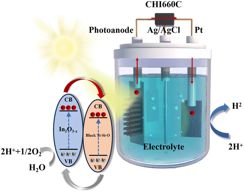
Fig. 10 illustrates the charge transfer mechanism in the In2O3−x/black Ti–Si–O composite photoanode. Upon illumination by solar light, photo-induced electron–hole pairs generated in the conduction and valence bands of both In2O3−x and black Ti–Si–O. Owing to the lower conduction and valence band positions of In2O3−x relative to black Ti–Si–O, a potential difference exists at the interface, facilitating the migration of photogenerated electrons from the conduction band of In2O3−x to that of black Ti–Si–O, thereby promoting effective electron accumulation. The photogenerated holes migrate from the valence band of black Ti–Si–O to the valence band of In2O3−x, thereby ensuring the effective separation of electron–hole pairs. Subsequently, the photogenerated electrons migrate to the platinum electrode surface under the applied electric field and react with H+ ions in the electrolyte to produce hydrogen gas. During the process of charge carrier transfer and separation, Si doping introduces impurity energy levels that not only promote the separation of carriers but also extend their lifetime. The presence of Ti3+/Vo defect energy levels alters the transport path of the photogenerated carriers, thereby facilitating their separation and transport. The In2O3−x composite leverages the difference in band positions between the two materials to further enhance the separation of photogenerated carriers and reduce their recombination probability. Consequently, the In2O3−x/black Ti–Si–O composite photoanode exhibits superior performance in photoelectrochemical water splitting for hydrogen production.
 | ||
| Fig. 10 Charge transfer mechanism of the In2O3−x/black Ti–Si–O photoanode. | ||
4. Conclusions
In this work, we successfully combined In2O3−x nanofilms with black Ti–Si–O nanotubes to fabricate a novel heterojunction for enhanced photoelectrochemical (PEC) water splitting performance. Black Ti–Si–O nanotube photoanodes were prepared through the reduction of Ti–Si–O nanotubes with tin, exhibiting high-efficiency photoelectrochemical performance due to Si doping and oxygen vacancies. The In2O3−x nanofilms deposited on the black Ti–Si–O photoanodes were fabricated through electrochemical deposition. Optical and PEC performance tests indicated that the photoanode at −1 V In2O3−x/black Ti–Si–O has the highest donor density, the narrowest bandgap, the smallest photogenerated charge carrier transport resistance, and the highest photocurrent density (3.76 mA cm−2), which was 2.16 times that of the black Ti–Si–O photoanode. The composite photoanode had great potential for low-cost hydrogen production. This work provides new insights into the preparation of TiO2-based composite catalysts with excellent photoelectrochemical performance.Data availability
The data that support the findings of this study are available on request from the corresponding author.Author contributions
Jianing Cui: experiments; writing – original draft preparation. Dongyan Ding: conceptualization; writing – review & editing; supervision; project administration. Shengzhe Yue: experiments; data curation. Zhi Chen: formal analysis.Conflicts of interest
The authors declare that they have no known competing financial interests or personal relationships that could have appeared to influence the work reported in this paper.Acknowledgements
This research was funded by SJTU-Zhongmu Joint Research Center for Materials and Technology of Intelligent and Connected Vehicles (no. 202310). We thank the contributions from SEM, XPS and UV-vis labs at Instrumental Analysis Center of SJTU.References
- K. Zhang, X. Huang, G. Peng, S. Li, S. Chandrasekaran and D. Zhong, et al., J. Alloys Compd., 2025, 1010, 178179 CrossRef.
- N. B. Trinh, T. A. Nguyen, S. V. Vu, H. G. Vo, T. N. Lo and I. Park, et al., RSC Adv., 2024, 14, 34037–34050 RSC.
- S. Cheng, Q. Liu, Z. Hu, C. Zhan, D. Fan and M. Li, et al., J. Phys. Chem. Solids, 2024, 193, 122122 CrossRef.
- N. A. Abdel-Hady, M. I. Badawy, M. S. Attia and T. A. Gad - Allah, RSC Adv., 2024, 14, 33666–33680 RSC.
- S. Chandrasekaran, L. Yao, L. Deng, C. Bowen, Y. Zhang and S. Chen, et al., Chem. Soc. Rev., 2019, 48, 4178–4280 RSC.
- S. Manzetti, T. Lu, H. Behzadi, M. D. Estrafili, H. Thi Le and H. Vach, RSC Adv., 2015, 5, 29159–29166 RSC.
- D. Lee, H. Shin and M. Yoon, RSC Adv., 2024, 14, 40180–40186 RSC.
- X. Chen, L. Liu, P. Y. Yu and S. S. Mao, Science, 2011, 331, 746–750 CrossRef PubMed.
- A. Fujishima and K. Honda, Nature, 1972, 238, 37–38 CrossRef PubMed.
- K. Nakata and A. Fujishima, J. Photochem. Photobiol., A, 2012, 13, 169–189 CrossRef.
- W. Sun, D. Wang, Z. U. Rahman, N. Wei and S. Chen, J. Alloys Compd., 2017, 695, 2154–2159 CrossRef.
- K. B. Koozegar, Opt. Quant. Electron., 2015, 47, 2075–2086 CrossRef.
- E. Musazade, R. Voloshin, N. Brady, J. Mondal, S. Atashova and S. K. Zharmukhamedov, et al., J. Photochem. Photobiol., C, 2018, 35, 23 CrossRef.
- M. J. Rivero, O. Iglesias, P. Ribao and I. Ortiz, Int. J. Hydrogen Energy, 2019, 44, 101–109 CrossRef.
- X. Liu, H. Lai, J. Li, G. Peng, Z. Yi, R. Zeng, M. Wang and Z. Liu, Int. J. Hydrogen Energy, 2019, 44, 4698–4706 CrossRef.
- X. Zhang, S. Cao, Z. Wu, S. Zhao and L. Piao, Appl. Surf. Sci., 2017, 402, 360–368 CrossRef CAS.
- B. Tahir, M. Tahir and N. A. S. Amin, Energy Convers. Manag., 2018, 159, 284–298 CrossRef CAS.
- M. A. Ahmed, J. Photochem. Photobiol., A, 2012, 238, 63–70 CrossRef CAS.
- Q. Wang, S. Zhu, Y. Liang, Z. Cui, X. Yang and C. Liang, et al., J. Nanoparticle Res., 2017, 19, 1–14 CrossRef.
- P. Filippatos, N. Kelaidis, M. Vasilopoulou, D. Davazoglou, N. N. Lathiotakis and A. Chroneos, Sci. Rep., 2019, 9, 1–10 CrossRef.
- X. Chen and C. Burda, J. Am. Chem. Soc., 2008, 130, 5018–5019 CrossRef.
- L. Wang, J. Han, J. Feng, X. Wang, D. Su and X. Hou, et al., Int. J. Hydrogen Energy, 2019, 44, 30899–30909 CrossRef.
- Y. Zhao, L. Nie, H. Yang, K. Song and H. Hou, Colloids Surf., 2021, 629, 127455 CrossRef.
- A. Knoks, J. Kleperis, G. Bajars, L. Grinberga and O. Bogdanova, Latv. J. Phys. Tech. Sci., 2021, 58, 24–34 Search PubMed.
- Y. Chen, A. Li, Q. Li, X. Hou and L. N. Wang, et al., J. Mater. Sci. Technol., 2018, 34, 955–960 CrossRef.
- C. Chen, Y. Wei, G. Yuan, Q. Liu, R. Lu and X. Huang, et al., Adv. Funct. Mater., 2017, 27, 1701575 CrossRef.
- Y. Su, S. Chen, X. Quan, H. Zhao and Y. Zhang, Appl. Surf. Sci., 2008, 255, 2167–2172 CrossRef.
- X. Yan, J. He, D. G. Evans, X. Duan and Y. X. Zhu, Appl. Catal., B, 2005, 55, 243–252 CrossRef.
- K. Yang, Y. Dai and B. Huang, Chem. Phys. Lett., 2008, 456, 71–75 CrossRef.
- Q. Zhao, Z. Liu, J. Li, W. Yan, J. Ya and X. Wu, Int. J. Hydrogen Energy, 2021, 46, 11 Search PubMed.
- Z. Wang, C. Yang, T. Lin, H. Yin, P. Chen and D. Wan, et al., Energy Environ. Sci., 2013, 6, 3007–3014 RSC.
- X. Chen, L. Liu and F. Huang, Chem. Soc. Rev., 2015, 44, 1861–1885 RSC.
- E. Wang, W. Yang and Y. Cao, J. Phys. Chem. C, 2009, 113, 20912–20917 CrossRef.
- H. Yang, J. Tian, Y. Bo, Y. Zhou, X. Wang and H. Cui, J. Colloid Interface Sci., 2017, 487, 258–265 CrossRef PubMed.
- C. Cao, C. Hu, W. Shen, S. Wang, J. Wang and H. Liu, et al., Sci. Adv. Mater., 2013, 5, 796–802 CrossRef.
- Z. Jiang, D. Jiang, Z. Yan, D. Liu, K. Qian and J. Xie, Appl. Catal., B, 2015, 17, 195–205 CrossRef.
- Y. C. Chen, Y. C. Pu and Y. J. Hsu, J. Phys. Chem. C, 2012, 116, 2967–2975 CrossRef.
- D. Chu, Y. Masuda, T. Ohji and K. Kato, Langmuir, 2010, 26, 14814–14820 CrossRef PubMed.
- J. Gan, X. Lu, J. Wu, S. Xie, T. Zhai and M. Yu, et al., Sci. Rep., 2013, 3, 1021 CrossRef.
- Z. Dong, D. Ding, T. Li and C. Ning, Int. J. Hydrogen Energy, 2019, 44, 17611–17621 CrossRef.
- H. Cui, W. Zhao, C. Yang, H. Yin, T. Lin and Y. Shan, et al., J. Mater. Chem., 2014, 2, 8612–8616 RSC.
- H. Khan and I. K. Swati, Ind. Eng. Chem. Res., 2016, 55, 6619–6633 CrossRef CAS.
- M. A. Butler, J. Appl. Phys., 1977, 48, 1914–1920 CrossRef CAS.
- J. Tauc, R. Grigorovici and A. Vancu, Phys. Status Solidi B, 1966, 15, 627–637 CrossRef CAS.
- B. Hou, K. Ou, Z. Zhu, X. Wu, H. Zhu and L. Liu, et al., Appl. Phys. A, 2024, 130, 934 CrossRef CAS.
- Y. Yuan, Y. Wang, G. Zhuang, Q. Li, F. Yang and X. Wang, et al., J. Mater. Chem. A, 2021, 9, 24909–24914 RSC.
- Y. Yang, L. Sun, W. Zhan, X. Wang and X. Han, J. Mater. Chem. A, 2021, 9, 4310–4316 RSC.
- K. Gelderman, L. Lee and S. W. Donne, J. Chem. Educ., 2007, 84, 685 CrossRef CAS.
- G. Wang, H. Wang, Y. Ling, Y. Tang, X. Yang and R. C. Fitzmorris, et al., Nano Lett., 2011, 11, 3026–3033 CrossRef CAS.
- Y. J. Hwang, A. Boukai and P. D. Yang, Nano Lett., 2009, 9, 410–415 CrossRef CAS PubMed.
- H. Cai, Q. Yang, Z. Hu, Z. Duan, Q. You and J. Sun, et al., Appl. Phys. Lett., 2014, 104, 53114 CrossRef.
- J. E. Carrera-Crespo, M. E. Rincon, F. Gonzalez, E. Barrera and I. Gonzalez, J. Solid State Electrochem., 2016, 20, 2713–2723 CrossRef.
| This journal is © The Royal Society of Chemistry 2025 |