
 Open Access Article
 This Open Access Article is licensed under a Creative Commons Attribution-Non Commercial 3.0 Unported Licence
Multifunctional acetoacetanilide additive strategy for enhanced efficiency and stability in perovskite solar cells
Abdullah Al Hossain Newaz a,
Anjan Kumarb,
Prakash Kanjariyac,
Asha Rajivd,
Aman Shankhyane,
Helen Merina Albertf,
Ahmed Mohsen*gj,
M. Atifh and
Mohammed El-Meligyik
a,
Anjan Kumarb,
Prakash Kanjariyac,
Asha Rajivd,
Aman Shankhyane,
Helen Merina Albertf,
Ahmed Mohsen*gj,
M. Atifh and
Mohammed El-Meligyik
aMasters of Science in Mechanical Engineering, University of Bridgeport, Bridgeport, Connecticut 06604, USA
bDepartment of Electronics and Communication Engineering, GLA University, Mathura-281406, India
cMarwadi University Research Center, Department of Physics, Faculty of Science, Marwadi University, Rajkot-360003, Gujarat, India
dDepartment of Physics & Electronics, School of Sciences, JAIN (Deemed to be University), Bangalore, Karnataka, India
eCentre for Research Impact & Outcome, Chitkara University Institute of Engineering and Technology, Chitkara University, Rajpura, Punjab 140401, India
fDepartment of Physics, Sathyabama Institute of Science and Technology, Chennai, Tamil Nadu, India
gRefrigeration & Air-condition Department, Technical Engineering College, The Islamic University, Najaf, Iraq. E-mail: ahmed.mohsen@rediffmail.com
hDepartment of Physics and Astronomy, College of Science, King Saud University, P. O. Box 2455, Riyadh 11451, Saudi Arabia
iJadara University Research Center, Jadara University, P. O. Box 733, Irbid, Jordan
jRefrigeration & Air-condition Department, College of Technical Engineering, the Islamic University of Al Diwaniyah, Al Diwaniyah, Iraq
kApplied Science Research Center, Applied Science Private University, Amman, Jordan
First published on 28th February 2025
Abstract
Perovskite solar cells (PSCs) have garnered tremendous interest for their cost-effective solution-based fabrication process and impressive power conversion efficiency (PCE). The performance and stability of PSCs are closely tied to the quality of the perovskite film. Additive engineering has emerged as a highly effective strategy to achieve stable and efficient PSCs. In this study, acetoacetanilide (AAA), containing amide and carbonyl groups, is introduced for the first time as a multifunctional agent to the MAPbI3 precursor solution. Carbonyl groups in AAA coordinate with lead ions (Pb2+), influencing the crystallization process by binding to Pb2+ ions through lone pair electrons. It helps to control crystallization kinetics and passivates defects caused by under-coordinated Pb2+ ions. Simultaneously, the amide groups strongly interact with iodide ions (I−), stabilizing them and suppressing ion migration, which reduces defect vacancies in the perovskite structure. Incorporating AAA led to a significant improvement in PCE, increasing from 16.93% in the untreated device to 20.1% in the AAA-treated devices. Furthermore, the AAA-treated devices showed more stability behavior against humidity and light. These findings underscore the potential of AAA as a high-performing additive for advancing the PCE and stability of PSCs.
1. Introduction
Perovskite solar cells (PSCs) consist of hybrid organic–inorganic perovskite (HOIP) materials with an ABX3 crystal structure as the absorber layer, where A represents an organic cation group (e.g., MA+, Cs+, and FA+), B is an inorganic cation (e.g., Pb2+ and Sn2+) and X is a halide ion (e.g., I−, Br−, and Cl−).1–4 HOIP materials were first applied in dye-sensitized solar cells by the Miyasaka research group, achieving an efficiency of 3.81% in 2009.1PSCs have garnered tremendous interest for their cost-effective solution-based fabrication process, and excellent optoelectronic properties.5–10 Their excellent optoelectronic properties include a high absorption coefficient, high mobility of carrier, low exciton binding energies, and tunable bandgap.11–17 PSCs have garnered significant interest from both academic and industrial sectors due to their strong potential for commercial applications and rapid advancement in PCE.18–21
Recent advancements in PSCs have led to significant improvements in device efficiency, with the highest reported PCE values reaching 26.5%.22 For instance, the development of solution-processed single-crystal MAPbI3 films enabled lower crystallization temperatures, leading to improved open-circuit voltages and efficiencies of up to 21.9%.23 Additionally, innovative defect passivation techniques, such as the spontaneous formation of a p–n homojunction using natural additives, achieving a PCE of 21.88%. Notably, these PCE values rank among the highest recorded for polycrystalline MAPbI3-based p-i-n PSCs reported to date.
Although significant progress has been made in the development of PSCs, further advancements in efficiency and stability are essential for their successful commercialization.24–27 The efficiency of PSCs appertains to the excellent quality of the perovskite film in terms of smooth morphology, absence of pinholes, minimal trap state density, large grain size, and high uniformity.28–32 These factors significantly influence efficient charge separation and collection, the diffusion length of perovskite film, long-term stability, charge carrier recombination, and charge mobility.33–35 However, thin perovskite films are fabricated using low-temperature solution processes, leading to defects such as grain boundaries, halide vacancies, and uncoordinated Pb2+ ions.28,32,36,37
As mentioned above, long-term stability remains a major challenge for PSC commercialization. Stability examination, including degradation rate evaluation (T80, T90) provide critical insight into PSCs lifetime under real-world condition. Additionally, energy yield, measure of actual power output over time, has emerged as a key performance metric.38 Notably, recent advancements in encapsulation, interfacial engineering, and defect passivation have significantly extended PSC stability, with some reports achieving over 90% PCE retention after 1000 h of operation.39 These advancements underscore the necessity of evaluating both efficiency and long-term performance for PSC commercialization.
In the past decade, numerous strategies have been devised to enhance stability and efficiency, such as interface engineering, anti-solvent techniques, additive engineering, etc.40–44 Among them, additive engineering, which involves incorporating small amounts of additives into the perovskite precursor solution, has proven to be a powerful strategy for controlling perovskite crystallization.28,45,46 This approach promotes the formation of larger grain sizes, minimizes the migration of mobile ions, and lowers trap densities in the perovskite film, leading to improved efficiency and stability of PSCs. A wide range of additives has been explored, including ammonium salts, polymers, Lewis acids and bases, low-dimensional perovskites, and ionic liquids.47–52 However, many of these additives typically contain a single functional group (e.g., amino, carbonyl, amide, phenethyl, and cyano) which can passivate only one or two types of defects in the perovskite structure.28,37,53,54
In contrast, passivation materials with multifunctional chemical group offer a unique advantage by addressing multiple challenges in PSCs simultaneously.40,55,56 These functional groups provide active sites that influence the crystallization process, passivate defects, and enhance the overall quality of perovskite films. For example, Li et al. used scandium trifluoromethanesulfonate (Sc(OTF)3) in the perovskite precursor solution as a multifunctional agent. This compound improved film morphology, extended charge carrier lifetimes, and stabilized methylamine ions through strong hydrogen bonding. As a result, the PSCs exhibited a high efficiency of 20.63%.57 Bi et al. developed benzoyl hydrazine (BH) as a multifunctional additive for PSCs. BH effectively reduced film defects, suppressed iodide migration, and reconverted I2 back to I− via its –NH–NH2 groups. These enhancements significantly improved device performance, achieving a PCE of 22.75%.58 Cao et al. introduced two multifunctional fluorinated propylamine salt 2,2,3,3,3-pentafluoropropylamine hydrochloride (PFPACl) and 3,3,3-triflupropylamine hydrochloride (TFPACl) into the perovskite precursor solution. These additives passivated defects and improved energy alignment with the hole transport layer, achieving a high PCE of 23.59%.59 Considering the above advantages, incorporating multifunctional additives into perovskite precursor solution is a promising strategy to effectively passivate various defects, thereby addressing key challenges in the field. Therefore, identifying novel multifunctional materials that can effectively passivate defects is essential for advancing PSCs' performance.
In this work, we reported the first use of acetoacetanilide (AAA) as a multifunctional additive in the MAPbI3 perovskite precursor solution. AAA, an organic compound with the formula C10H11NO2, contains both amide (–CONH–) and carbonyl (–C![[double bond, length as m-dash]](https://www.rsc.org/images/entities/char_e001.gif) O) functional groups which make it an effective additive for addressing key issues in PSCs, such as high defect densities, ion migration, and moisture instability. The carbonyl groups in AAA coordinate with lead ions (Pb2+), influencing the crystallization process by binding to Pb2+ ions through lone pair electrons. This coordination regulates the crystallization kinetics of the perovskite and passivates defects caused by under-coordinated Pb2+ ions. Simultaneously, the amide groups strongly interact with iodide ions (I−), stabilizing them and suppressing ion migration, thereby reducing defect vacancies in the perovskite structure. These synergistic effects lead to enhanced the morphology, improved charge transport properties, and increase device stability. Consequently, treated PSCs with 2.0 mol% of AAA exhibit a notable improvement in PCE, from 16.93% in untreated devices to 20.1% in devices treated with 2.0 mol% AAA, along with enhanced operational stability under environmental conditions. Our findings underscore the potential of AAA as a high-performance additive for advancing both the efficiency and stability of PSCs. This study provides new insights into the role of multifunctional additives in perovskite film formation and defect passivation, contributing to the ongoing development of commercially viable PSC technologies.
O) functional groups which make it an effective additive for addressing key issues in PSCs, such as high defect densities, ion migration, and moisture instability. The carbonyl groups in AAA coordinate with lead ions (Pb2+), influencing the crystallization process by binding to Pb2+ ions through lone pair electrons. This coordination regulates the crystallization kinetics of the perovskite and passivates defects caused by under-coordinated Pb2+ ions. Simultaneously, the amide groups strongly interact with iodide ions (I−), stabilizing them and suppressing ion migration, thereby reducing defect vacancies in the perovskite structure. These synergistic effects lead to enhanced the morphology, improved charge transport properties, and increase device stability. Consequently, treated PSCs with 2.0 mol% of AAA exhibit a notable improvement in PCE, from 16.93% in untreated devices to 20.1% in devices treated with 2.0 mol% AAA, along with enhanced operational stability under environmental conditions. Our findings underscore the potential of AAA as a high-performance additive for advancing both the efficiency and stability of PSCs. This study provides new insights into the role of multifunctional additives in perovskite film formation and defect passivation, contributing to the ongoing development of commercially viable PSC technologies.
2. Experimental
2.1 Material
Methylene ammonium iodide (MAI, 97%, Sigma-Aldrich), lead(II) iodide (PbI2, 99.8%, Lumtec), anhydrous dimethyl sulfoxide (DMSO, 99.5%, Sigma-Aldrich), anhydrous N,N-dimethylformamide (DMF, 99.8%, Merck), isopropyl alcohol (IPA, 99.8%, Sigma-Aldrich), anhydrous ethyl acetate (EA, 99.8%, Sigma-Aldrich), ethanol (EtOH, 99.8%, Merck), titanium(IV) isopropoxide (TTIP, 99.8%, Sigma-Aldrich), spiro-OMeTAD (99%, Sigma-Aldrich), bis(trifluoromethane)sulfonimide lithium salt (LiTFSI, >97%, Sigma-Aldrich), 4-tert-butylpyridine (t-BP, 98%, Merck), anhydrous acetonitrile (AC, 99.95%), acetoacetanilide (AAA, 99.5%, Sigma-Aldrich) were purchased. FTO substrate and commercial TiO2 paste were purchased from Dyesol.2.2 Device fabrication
The FTO-coated glasses were sequentially washed with a detergent solution, deionized water, acetone, and isopropanol in an ultrasonic bath. Cleaned and dried FTO substrates were treated with UV–ozone for 20 min. A compact titanium dioxide (c-TiO2) layer was formed on the FTO substrate by spin-coating 45 μL of TTIP + IPA (65 mg mL−1) at a speed of 4200 rpm for 30 s, then annealing at 450 °C for 30 min. Mesoporous TiO2 (mp-TiO2) was employed as an electron transport layer (ETL). It is coated on the c-TiO2 layer at a speed of 3400 rpm for 30 s and then baked at 500 °C for 45 min. The perovskite precursor solution was prepared by dissolving PbI2 (1.68 M, 0.755 g), MAI (1.60 M, 0.179 g), and DMSO (1.6 M, 0.114 mL) in 1 mL of DMF under stirring at 70 °C for 30 min. The perovskite + AAA solution was prepared similarly, except that different concentrations of AAA (e.g., 0.5, 1.0, 2.0, and 4.0 mol% relative to the PbI2) were added directly to the precursors before the DMF addition. The perovskite film was deposited using a two-step spin-coating procedure: first at 1000 rpm for 10 s followed by 4500 rpm for 20 s. In the middle of the second step, 200 μL of EA was poured onto the spinning substrate and then annealed at 150 °C for 30 min. Spiro-OMeTAD as hole transport layer (HTL) was spin coated over the perovskite layer at 3000 rpm for 30 s. The spiro-OMeTAD precursor solution was papered by dissolving 72.3 mg of spiro-OMeTAD in 1 mL of chlorobenzene. Then, 35 μL of LiTFS (from a stock solution containing 520 mg in 1 mL of AC) and 17.5 μL of 4-TBP were added to the solution. A thin layer of Au was Finally deposited by thermal evaporation onto HTL to serve as the back electrode.2.3 Characterizations
FESEM TESCAN MIRA4 microscope captured FESEM images of samples. X-ray photoelectron spectroscopy (XPS) test was conducted for samples with a Thermo Fisher Scientific, ESCALAB 250Xi XPS instrument. Crystalline phases of perovskite samples were recorded by D8 Bruker XRD. UV-Vis spectra of samples were recorded using Jasco V-670 spectrometer. Steady-state photoluminescence (PL) spectra of samples were investigated using an Edinburgh, FLS980 with a excitation wavelength of 530 nm. Time-resolved photoluminescence (TRPL) spectra of samples were measured using a Horiba Quantamaster 800 fluorometer. Current–voltage density curve (J–V) measurement were investigated using Keithley 2400 source under class AAA illumination from a Newport-Oriel simulator EIS of samples were recorded using a P1 ZIVE electrochemical instrument at open-circuit condition. Active area of samples to measure EIS response was 2 mm × 8 mm. Enlitech QE-R system measured EQE spectra of devices.3. Results and discussion
Fig. 1a illustrates the chemical structure of AAA, a compound from the β-diketone family featuring an aniline-derived amide group. This structure consists of both amide (–CONH–) and carbonyl (–CO) functional groups. It is assumed that the carbonyl groups coordinate with Pb2+ via their lone pair electrons, influencing the crystallization and passivating defects. Furthermore, we hypotheses that the amide groups can form strong interaction with iodide ions (I−), stabilizing these ions and suppressing ion migration, thereby reducing defect vacancies in the perovskite structure. To validate this hypothesis, AAA was applied to the MAPbI3 precursor as an agent, and the resulting solution was spin-coated using a two-step procedure.
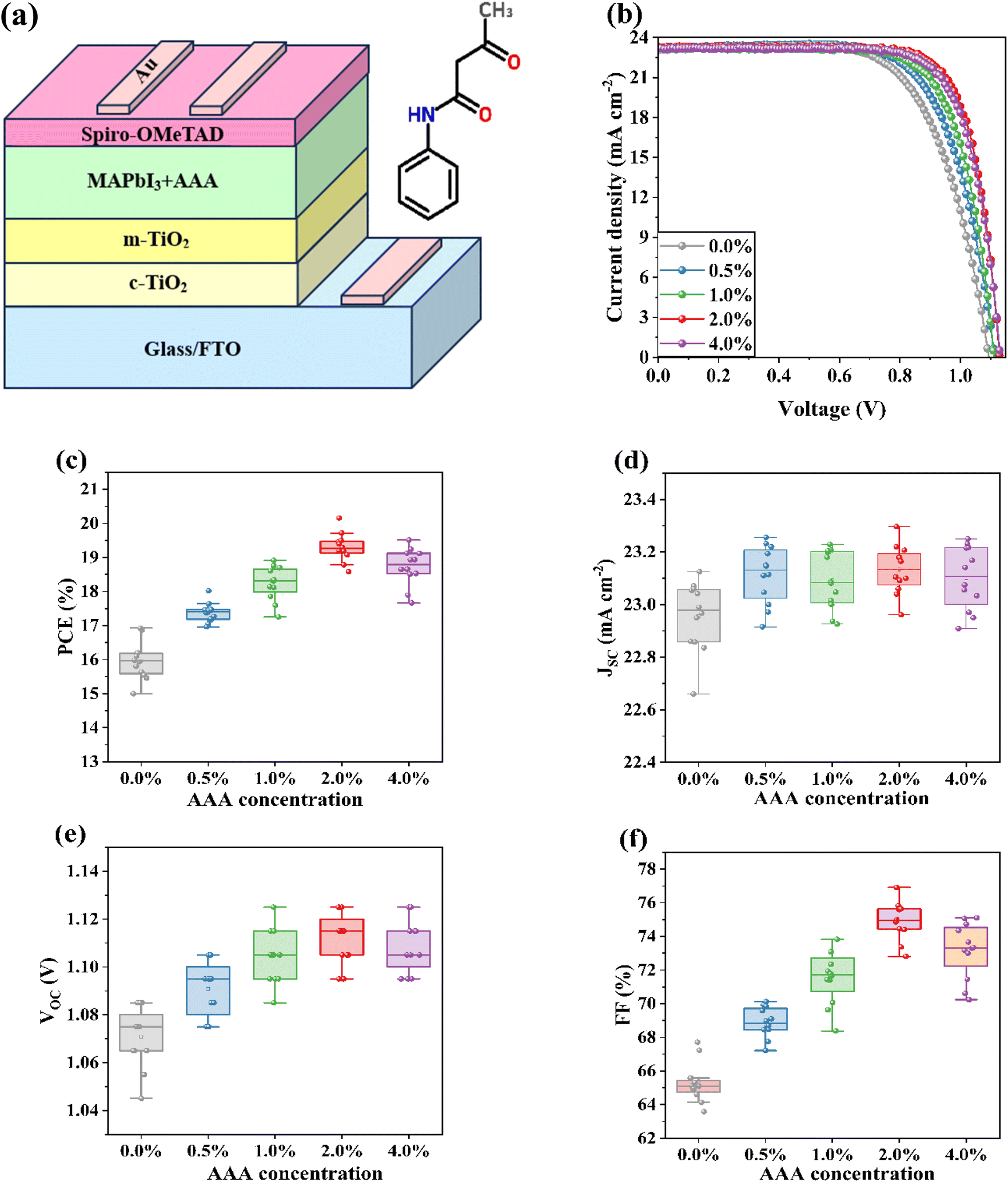 | ||
| Fig. 1 (a) Chemical structure of AAA and schematic of the fabricated device. (b) J–V curves of the untreated PSCs and treated PSCs with varying concentrations of AAA. Statistical distribution of photovoltaic parameters for untreated PSCs and treated PSCs as a function of AAA concentration: (c) PCE, (d) JSC, (e) VOC, (f) FF. | ||
Initially, to investigate the impact of incorporating AAA as an additive on photovoltaic performance and optimize additive concentration, PSCs were fabricated with the structure glass/FTO/TiO2/MAPbI3 + AAA/spiro-OMeTAD/Au, as illustrated in Fig. 1a. The treated PSCs were prepared with additive concentrations of 0.5, 1.0, 2.0, and 4.0 mol%. In contrast, the untreated PSCs were fabricated similarly without any additive.
The J–V curves of the champion PSCs with varying concentrations of AAA (0.0, 0.5, 1.0, 2.0, and 4.0 mol%) were measured under air mass (AM) 1.5 G illumination under an intensity of 100 mW cm−2, and shown in Fig. 1b. The champion and average photovoltaic parameters, including PCE, short circuit voltage (JSC), open circuit voltage (VOC), and fill factor (FF) were also extracted and are summarized in Table 1. Additionally, the statistical distribution of these photovoltaic parameters as a function of AAA concentration is presented in the box plots shown in Fig. 1c and d. As the results show, the untreated device achieved a champion efficiency of 16.93% with a JSC of 23.04 mA cm−2, a VOC of 1.085 V, and an FF of 67.71%. All devices treated with various additive concentrations exhibited higher average values for all photovoltaic parameters than untreated devices. As expected, the enhanced photovoltaic performance of PSCs incorporating the AAA additive particularly in VOC and FF can be attributed to its multifunctional benefits. The carbonyl groups of AAA interact with uncoordinated Pb2+ ions, improving perovskite crystallization while simultaneously passivating defects caused by under-coordinated Pb2+ ions. Additionally, the amide groups strongly interact with I− ions, effectively reducing defect vacancies in the perovskite structure. These combined effects significantly enhance overall device performance by lowering trap density, suppressing non-radiative charge recombination, and improving charge transfer within the device, thereby improved FF and VOC with a slight increase in JSC.
| Device | PCE (%) | JSC (mA cm−2) | FF (%) | VOC (V) | |
|---|---|---|---|---|---|
| a Av. indicates average and Cham. indicates champion. | |||||
| 0.0% | Av. | 16.05 | 22.96 | 65.29 | 1.071 |
| Cham. | 16.93 | 23.04 | 67.71 | 1.085 | |
| 0.5% | Av. | 17.37 | 23.11 | 68.89 | 1.091 |
| Cham. | 18.02 | 23.26 | 70.13 | 1.105 | |
| 1.0% | Av. | 18.24 | 23.09 | 71.55 | 1.105 |
| Cham. | 18.92 | 23.21 | 73.10 | 1.115 | |
| 2.0% | Av. | 19.30 | 23.14 | 74.95 | 1.113 |
| Cham. | 20.16 | 23.29 | 76.91 | 1.125 | |
| 4.0% | Av. | 18.73 | 23.10 | 73.17 | 1.108 |
| Cham. | 19.52 | 23.22 | 74.73 | 1.125 | |
Notably, as the additive concentration increased from 0.0 to 2.0 mol%, the champion PCE improved significantly, reaching a maximum of 20.16%. However, further increasing the additive concentration to 4.0% resulted in a slight decline in PCE to 19.52%. Therefore, the device treated with 2.0 mol% AAA exhibited the best overall improvement, achieving an efficiency of 20.16% with a JSC of 23.29 mA cm−2, VOC of 1.125 V, and FF of 76.91%. These observations can be attributed to the fact that at lower concentrations, the amount of AAA available for interact with Pb2+ and I− ions in the perovskite may be inadequate. Without sufficient interaction, AAA can't efficiently improve the crystal quality, grain size, suppress non-radiative charge recombination or charge transport properties of the perovskite, all of which are essential for achieving higher PCE. On the other hand, at higher concentrations, insulating nature of AAA can limit charge transport, thereby hinder performance. Consequently, the optimum concentration for AAA was determined to be 2.0 mol%. A systematic characterization was conducted to confirm the AAA additive significantly improves the photovoltaic performance of PSCs treated with AAA. In the following experiments, all procedures were carried out using an additive concentration of 2.0 mol% as it corresponded to the highest PCE.
To evaluated the hysteresis effect, the J–V curves of untreated and AAA-treated PSCs were recorded at a scanning rate of 0.1 V s−1 as presented in Fig. 2a and photovoltaic parameters are summarized in Table 2. The hysteresis index was calculated according to the formula of [HI = (PCEreverse − PCEforward)/PCEreverse] for the typical devices with and without AAA additive.60 The negligible hysteresis observed in the reverse and forward scans of PSCs with AAA indicates that the AAA additive efficiently passivates defects, reduces trap states and grain boundaries. Furthermore, the amide groups in AAA can facilitate the retention of mobile iodide ions in MAPbI3 through hydrogen-bonding interactions.
 | ||
| Fig. 2 (a) J–V curves of untreated and treated with 2.0 mol% AAA PSCs measured by forward and reverse direction at of 0.1 V s−1. (b) EQE spectra untreated and treated with 2.0 mol% AAA PSCs. | ||
| Device | PCE (%) | JSC (mA cm−2) | FF (%) | VOC (V) | HI (%) | |
|---|---|---|---|---|---|---|
| 0.0% | Reverse | 16.93 | 23.04 | 67.71 | 1.085 | 20.69 |
| Forward | 14.03 | 22.89 | 59.22 | 1.035 | ||
| 2.0% | Reverse | 20.16 | 23.29 | 76.91 | 1.125 | 7.17 |
| Forward | 18.81 | 23.10 | 73.03 | 1.115 |
To further confirm the enhancement in photovoltaic performance, EQE measurements were conducted for both untreated and treated PSCs with 2.0 mol% AAA (Fig. 2b). The EQE spectra reveal a slight enhancement in photon-to-current conversion efficiency across a wavelength range of 340 to 760 nm for the device traded compared to the untreated device, which is consistent with the slight increase in JSC observed in the J–V data. The integrated JSC (JIn) values obtained from the EQE measurements for untreated and treated PSCs are 22.86 and 23.12 mA cm−2, respectively. These values align well with the JSC obtained from J–V curves. The higher JIn for the traded PSCs can be attributed to the enhanced crystallinity of the MAPbI3.
The impact of AAA on the morphology of surface and crystallization of perovskite film was investigated using FESEM and XRD measurements. Top-view SEM images of untreated perovskite film and film treated with 2.0 mol% AAA are shown in Fig. 3a and b, respectively. The treated perovskite film exhibits excellent morphology with larger grain sizes and enhanced uniformity, unlike the untreated film, which displays a nonuniform morphology with numerous grain boundaries and a rough surface. Results suggest that AAA plays a crucial role in controlling the quality and morphology of perovskite film. Fig. 3c and d show the size distribution histograms of the fabricated perovskite films without and with 2.0 mol% of AAA. As shown in the histograms, the grain size distribution of untreated film has random and a big difference in size values with the smaller grain size compared to treated film by AAA.
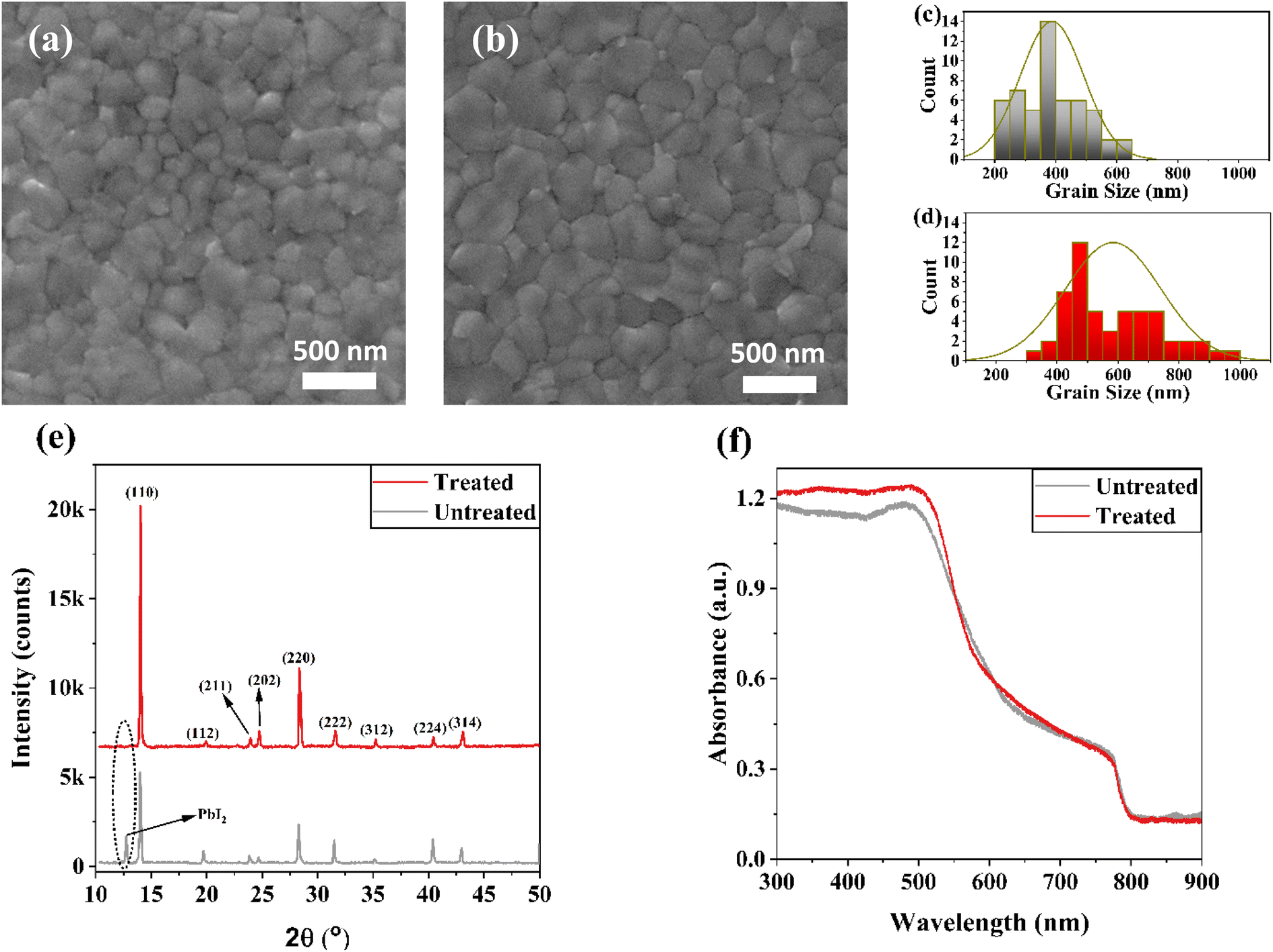 | ||
| Fig. 3 Top-view SEM images of (a) untreated perovskite film and (b) perovskite film treated with 2.0 mol% AAA. Grain size distribution histogram of (c) untreated and (d) treated perovskite films. (e) XRD patterns of the untreated and treated perovskite film with 2.0 mol% AAA. (f) UV-Vis spectra of the untreated and treated perovskite film with 2.0 mol% AAA. | ||
Fig. 3e shows the XRD patterns of untreated and treated perovskite films with 2.0 mol% AAA. Both treated and untreated perovskite films exhibit the same diffraction peaks at 14.06°, 19.81°, 23.95°, 24.76°, 28.38°, 31.58°, 35.26°, 40.47°, and 43.09°, corresponding to crystallographic planes of (110), (112), (211), (202), (220), (222), (312), (224), and (314), respectively.61 This finding indicates that the additive does not affect the crystal phase structure of the MAPbI3. However, the intensity of peaks of the treated perovskite film at 14.06° and 28.38° is stronger than those of the untreated film, indicating higher crystal orientation along the (110) and (220) directions. Additionally, the peak intensity at 12.68°, corresponding to the unreacted PbI2, is suppressed in the XRD pattern of treated perovskite film. These observations confirm that incorporating AAA into the MAPbI3 precursor solution significantly improves the crystallinity of the MAPbI3 film. This improvement is attributed to the powerful interactions between amide and carbonyl groups in AAA and the Pb2+ cations in the perovskite, which accelerate nucleation and delay crystallization during the film growth process, as evidenced by the enlarged perovskite grains observed in the SEM images.43,62
UV-Vis absorption spectra of both the untreated and treated perovskite film are shown in Fig. 3f. The treated perovskite film with 2.0 mol% AAA exhibited higher absorptance compared to the untreated film. This enhancement in light harvesting is due to the improved crystallinity and enlarged grain sizes of the MAPbI3 film, which is in good agreement with the higher JSC of treated devices.
To investigate the interaction between AAA and perovskite, XPS measurements were conducted to understand the compositional and chemical changes of the treated perovskite film. The XPS spectra of the N 1s, O 1s, Pb 4f, and I 3d core levels are shown in Fig. 4a–d. As seen in the N 1s spectra, a peak at 402.6, attributed to the C–N bond in the perovskite, shifted to a lower binding energy of 400.7 eV after the introduction of AAA (Fig. 4a). In addition, a peak appears at 402.8 eV in the treated perovskite film, confirming the incorporation of AAA in perovskite film. The two peaks at 532.2 and 534.1 in the spectrum of the treated perovskite film are assigned to O 1s from the CO and C–O groups in AAA, respectively. In contrast, no peaks are observed in O 1s of the untreated perovskite film, confirming the successful introduction of AAA into the perovskite film (Fig. 4b). As shown in Fig. 4c, the untreated perovskite film exhibited two main peaks of I 3d at binding energies of 619.2 and 630.7 eV. In contrast, these peaks shifted to higher binding energies of 619.5 and 631.0 eV, respectively, after incorporating AAA into perovskite film. For Pb 4f, two characteristic peaks appeared at 138.2 and 143.1 eV also shifted to higher binding energies of 138.4 and 143.3 eV upon the addition of AAA (Fig. 4d). The shift to higher binding energy is attributed to changes in the electron cloud density, indicating a chemical interaction between AAA and perovskite.63 Furthermore, the peaks detected at binding energies of 136.8 and 141.9 eV in the untreated perovskite film are associated with metallic lead (Pb0).64 Pb0 (formed when Pb2+ ions accept electrons) acts as a deep trap state creating non-radiative recombination center in the MAPbI3 film.37 The absence of Pb0 peaks in the spectrum of the treated perovskite film confirms that AAA effectively suppresses non-radiative recombination. The XPS results confirm that the carbonyl and amide functional groups of AAA interact with Pb2+ and I− in MAPbI3, effectively passivating defects in the perovskite film and enhancing its quality.
 | ||
| Fig. 4 High resolution XPS spectra of (a) N 1s, (b) O 1s, (c) I 3d, and (d) Pb 4f core levels for untreated and treated perovskite films with 2.0 mol% AAA. | ||
The impact of AAA on defect passivation and charge carrier transport was studied using PL and TRPL decay measurements. Perovskite films without and with 2.0 mol% AAA were deposited on glass substrates for TRPL and PL. As shown in Fig. 5a, the PL emission intensity of the perovskite film with the additive increased significantly compared to the untreated perovskite film, confirming the suppression of non-radiative recombination via defect passivation and reduced trap states. In addition, a blue shift was observed in the treated sample, which can be attributed to the passivating effect of the AAA additive. This additive effectively fills defects and reduces the density of shallow traps.65–67 The TRPL spectra of untreated and 2.0 mol% AAA-treated perovskite films are shown in Fig. 5b. By fitting the TRPL decays, the average lifetime of the untreated and AAA-treated perovskite films were calculated as 510.08 and 1538.53 ns, respectively.68 The enhanced PL intensity and longer lifetime of the treated perovskite film indicate suppressed non-radiative charge recombination, boosting FF and VOC as observed in the J–V curves.
 | ||
| Fig. 5 (a) PL and (b) TRPL spectra of different perovskites deposited on glass. | ||
EIS was utilized to further investigate charge carrier transport and recombination in both untreated and treated devices. Fig. 6 illustrates the Nyquist plots of untreated devices and those treated with 2.0 mol% AAA, measured at open-circuit voltage under dark conditions over a frequency range of 1 Hz to 3 MHz. The inset of Fig. 6 depicts the equivalent circuit model used for EIS fitting, which comprises series resistance (RS), charge transport resistance (RCt), and recombination resistance (RRec). The Nyquist plots exhibit two distinct arcs corresponding to different frequency regions. The smaller arc in the high-frequency region is attributed to the charge transport resistance RCt, which arises from the interfacial contact resistance, and is in parallel with the chemical capacitance (C1).69 In contrast, the larger arc in the low-frequency region represents recombination resistance (RRec), related to electron recombination within the ETL and perovskite layer, in parallel with the chemical capacitance (C2).70 Furthermore, RS denotes the series resistant, which primarily from the sheet resistance of the FTO and the contact resistance within the device.71
 | ||
| Fig. 6 EIS spectra of untreated and treated PSCs with 2.0 mol% AAA, measured at open-circuit voltage under dark conditions. | ||
Long-term stability is a crucial issue in the development and commercialization of PSCs. Accordingly, the effect of the AAA additive on environmental stability was studied under dark conditions at room temperature and in ambient air with a relative humidity of 30% for 2096 h. As shown in Fig. 7a, the device treated with 2.0 mol% AAA retained 84.2% of its initial PCE after 2096 h, whereas the untreated device dropped to 67.5% of its initial PCE over the same period, demonstrating that AAA significantly enhanced the humidity stability of PSCs. The enhanced stability of the MAPbI3 film is attributed to the high quality of perovskite film, fewer defects, and suppressed ion migration induced by the AAA additive. In addition, light stability of devices based on ISOS-L-1I protocol was measured in an inert environment (Fig. 7b). The treated retained 86.5% of its initial PCE after 576 h, whereas the untreated device dropped to 69% of its initial PCE just after 144 h, indicating that AAA significantly enhanced the light stability of PSCs. The reason behind stability improvements is the Pb2+ and I− passivation caused by the AAA additive, which improves perovskite quality and hinders ion migration during operational conditions. Besides, the enlarged grains in the treated perovskite layer block humidity and oxygen diffusion to the perovskite layer and thereby hinder perovskite degradation.72,73
 | ||
| Fig. 7 (a) Long-term ambient air stability and (b) operational light stability of untreated and treated PSCs with 2.0 mol% AAA. | ||
4. Conclusion
In summary, the multifunctional compound AAA, containing both amide and carbonyl functional groups, was successfully incorporated into MAPbI3 perovskite precursor solution for the first time as a high-performance agent to enhance PCE and stability of PSCs. We demonstrated that the carbonyl group coordinates with Pb2+ ions via their lone pair electrons, influencing crystallization and passivating defects. Simultaneously, the amide groups form strong interactions with I− ions, stabilizing them and suppressing ion migration, thereby reducing defect vacancies in the perovskite film. PL, TRPL, and EIS analysis confirmed that the AAA additive reduces defects in perovskite, suppresses charge recombination, facilitates charge transfer. As a result, the device treated with AAA achieved an improved PCE of 20.16%, compared to 16.93% for the untreated device. Furthermore, the treated device retained 84.2% of its initial PCE after 2096 h under environmental conditions, attributing the high quality of MAPbI3 film, fewer defects, and suppressed ion migration induced by the AAA additive. This work presents a simple and efficient strategy utilizing multifunctional organic compounds with a multi-passivation role to fabricate stable and efficient PSCs.Data availability
The data that support the findings of this study are available from the corresponding author upon reasonable request.Author contributions
All authors contributed equally in this paper.Conflicts of interest
The authors declare that they have no conflict of interest.Acknowledgements
The authors present their appreciation to King Saud University for funding this research through Researchers Supporting Project number (RSP2025R397), King Saud University, Riyadh, Saudi Arabia.References
- A. Kojima, K. Teshima, Y. Shirai and T. Miyasaka, J. Am. Chem. Soc., 2009, 131, 6050–6051 CrossRef CAS PubMed.
- L. Mao, C. C. Stoumpos and M. G. Kanatzidis, J. Am. Chem. Soc., 2018, 141, 1171–1190 CrossRef PubMed.
- D. Sirbu, F. H. Balogun, R. L. Milot and P. Docampo, Adv. Energy Mater., 2021, 11, 2003877 CrossRef CAS.
- B. Saparov and D. B. Mitzi, Chem. Rev., 2016, 116, 4558–4596 CrossRef CAS PubMed.
- Q. Wali, F. J. Iftikhar, M. E. Khan, A. Ullah, Y. Iqbal and R. Jose, Org. Electron., 2020, 78, 105590 CrossRef CAS.
- Research-cell efficiency chart, https://www.nrel.gov/pv/cellefficiency Search PubMed.
- J. J. Yoo, G. Seo, M. R. Chua, T. G. Park, Y. Lu, F. Rotermund, Y.-K. Kim, C. S. Moon, N. J. Jeon and J.-P. Correa-Baena, Nature, 2021, 590, 587–593 CrossRef CAS PubMed.
- J. Jeong, M. Kim, J. Seo, H. Lu, P. Ahlawat, A. Mishra, Y. Yang, M. A. Hope, F. T. Eickemeyer and M. Kim, Nature, 2021, 592, 381–385 CrossRef CAS PubMed.
- Z. Li, B. Li, X. Wu, S. A. Sheppard, S. Zhang, D. Gao, N. J. Long and Z. Zhu, Science, 2022, 376, 416–420 CrossRef CAS.
- Q. Jiang, J. Tong, Y. Xian, R. A. Kerner, S. P. Dunfield, C. Xiao, R. A. Scheidt, D. Kuciauskas, X. Wang and M. P. Hautzinger, Nature, 2022, 611, 278–283 CrossRef CAS.
- T. M. Brenner, D. A. Egger, L. Kronik, G. Hodes and D. Cahen, Nat. Rev. Mater., 2016, 1, 1–16 Search PubMed.
- D. Shi, V. Adinolfi, R. Comin, M. Yuan, E. Alarousu, A. Buin, Y. Chen, S. Hoogland, A. Rothenberger and K. Katsiev, Science, 2015, 347, 519–522 CrossRef CAS PubMed.
- M. B. Johnston and L. M. Herz, Acc. Chem. Res., 2016, 49, 146–154 CrossRef CAS PubMed.
- K. P. Ong, S. Wu, T. H. Nguyen, D. J. Singh, Z. Fan, M. B. Sullivan and C. Dang, Sci. Rep., 2019, 9, 2144 CrossRef.
- G. Xing, N. Mathews, S. Sun, S. S. Lim, Y. M. Lam, M. Grätzel, S. Mhaisalkar and T. C. Sum, Science, 2013, 342, 344–347 CrossRef CAS.
- S. D. Stranks, G. E. Eperon, G. Grancini, C. Menelaou, M. J. Alcocer, T. Leijtens, L. M. Herz, A. Petrozza and H. J. Snaith, Science, 2013, 342, 341–344 CrossRef CAS PubMed.
- M. Shao, T. Bie, L. Yang, Y. Gao, X. Jin, F. He, N. Zheng, Y. Yu and X. Zhang, Adv. Mater., 2022, 34, 2107211 CrossRef CAS.
- F. P. García de Arquer, A. Armin, P. Meredith and E. H. Sargent, Nat. Rev. Mater., 2017, 2, 1–17 Search PubMed.
- Y. Jiang, C. Qin, M. Cui, T. He, K. Liu, Y. Huang, M. Luo, L. Zhang, H. Xu and S. Li, Nat. Commun., 2019, 10, 1868 CrossRef PubMed.
- M. A. Green, E. D. Dunlop, M. Yoshita, N. Kopidakis, K. Bothe, G. Siefer, X. Hao and J. Y. Jiang, Prog. Photovolt., 2024, 425–441 CrossRef.
- C. Yang, W. Hu, J. Liu, C. Han, Q. Gao, A. Mei, Y. Zhou, F. Guo and H. Han, Light: Sci. Appl., 2024, 13, 227 CrossRef CAS.
- National Renewable Energy Laboratory (NREL), https://www.nrel.gov/pv/cell-efficiency.html, accessed 1/30/ 2025.
- A. Y. Alsalloum, B. Turedi, X. Zheng, S. Mitra, A. A. Zhumekenov, K. J. Lee, P. Maity, I. Gereige, A. AlSaggaf and I. S. Roqan, ACS Energy Lett., 2020, 5, 657–662 CrossRef CAS.
- Y. Wu, Q. Wang, Y. Chen, W. Qiu and Q. Peng, Energy Environ. Sci., 2022, 15, 4700–4709 RSC.
- T. Bu, J. Li, H. Li, C. Tian, J. Su, G. Tong, L. K. Ono, C. Wang, Z. Lin and N. Chai, Science, 2021, 372, 1327–1332 CrossRef CAS.
- Z. Yang, W. Zhang, S. Wu, H. Zhu, Z. Liu, Z. Liu, Z. Jiang, R. Chen, J. Zhou and Q. Lu, Sci. Adv., 2021, 7, eabg3749 CrossRef CAS.
- X. Li, F. Zhang, J. Wang, J. Tong, T. Xu and K. Zhu, Nat Sustainability, 2021, 4, 1038–1041 CrossRef.
- Y. Cai, J. Cui, M. Chen, M. Zhang, Y. Han, F. Qian, H. Zhao, S. Yang, Z. Yang and H. Bian, Adv. Funct. Mater., 2021, 31, 2005776 CrossRef CAS.
- G. A. Al-Dainy, S. E. Bourdo, V. Saini, B. C. Berry and A. S. Biris, Energy Technol., 2017, 5, 373–401 CrossRef CAS.
- Y.-H. Wu, X.-Q. Shi, X.-H. Ding, Y.-K. Ren, T. Hayat, A. Alsaedi, Y. Ding, P. Xu and S.-Y. Dai, ACS Appl. Mater. Interfaces, 2018, 10, 3602–3608 CrossRef CAS PubMed.
- F. Liu, Q. Dong, M. K. Wong, A. B. Djurišić, A. Ng, Z. Ren, Q. Shen, C. Surya, W. K. Chan and J. Wang, Adv. Energy Mater., 2016, 6, 1502206 CrossRef.
- C. Chen, Z. Song, C. Xiao, D. Zhao, N. Shrestha, C. Li, G. Yang, F. Yao, X. Zheng and R. J. Ellingson, Nano Energy, 2019, 61, 141–147 CrossRef CAS.
- H. Li, G. Wu, W. Li, Y. Zhang, Z. Liu, D. Wang and S. Liu, Advanced Science, 2019, 6, 1901241 CrossRef CAS PubMed.
- W. Ke, C. Xiao, C. Wang, B. Saparov, H.-S. Duan, D. Zhao, Z. Xiao, P. Schulz, S. P. Harvey and W. Liao, Adv. Mater., 2016, 28, 5214–5221 CrossRef CAS PubMed.
- N. J. Jeon, J. H. Noh, Y. C. Kim, W. S. Yang, S. Ryu and S. I. Seok, Nat. Mater., 2014, 13, 897–903 CrossRef CAS.
- B. Yang, J. Suo, D. Bogachuk, W. Kaiser, C. Baretzky, O. Er-Raji, G. Loukeris, A. A. Alothman, E. Mosconi and M. Kohlstädt, Energy Environ. Sci., 2024, 17, 1549–1558 RSC.
- B. Chen, P. N. Rudd, S. Yang, Y. Yuan and J. Huang, Chem. Soc. Rev., 2019, 48, 3842–3867 RSC.
- O. Almora, G. C. Bazan, C. I. Cabrera, L. A. Castriotta, S. Erten-Ela, K. Forberich, K. Fukuda, F. Guo, J. Hauch and A. W. Ho-Baillie, Adv. Energy Mater., 2024, 2404386 CrossRef.
- Q. Fu, X. Tang, B. Huang, T. Hu, L. Tan, L. Chen and Y. Chen, Adv. Sci., 2018, 5, 1700387 CrossRef PubMed.
- E. Khorshidi, B. Rezaei, D. Blätte, A. Buyruk, M. A. Reus, J. Hanisch, B. Böller, P. Müller-Buschbaum and T. Ameri, Sol. RRL, 2022, 6, 2200023 CrossRef CAS.
- E. Khorshidi, B. Rezaei, A. Kavousighahfarokhi, J. Hanisch, M. A. Reus, P. Muller-Buschbaum and T. Ameri, ACS Appl. Mater. Interfaces, 2022, 14, 54623–54634 CrossRef CAS.
- E. Khorshidi, B. Rezaei, N. Irannejad, S. Adhami, M. Ebrahimi, A. Kermanpur and A. A. Ensafi, Electrochim. Acta, 2020, 337, 135822 CrossRef CAS.
- Y.-J. Kang, S.-N. Kwon, S.-P. Cho, Y.-H. Seo, M.-J. Choi, S.-S. Kim and S.-I. Na, ACS Energy Lett., 2020, 5, 2535–2545 CrossRef CAS.
- S. Teale, M. Degani, B. Chen, E. H. Sargent and G. Grancini, Nat. Energy, 2024, 9, 779–792 CrossRef CAS.
- S. Bai, P. Da, C. Li, Z. Wang, Z. Yuan, F. Fu, M. Kawecki, X. Liu, N. Sakai and J. T.-W. Wang, Nature, 2019, 571, 245–250 CrossRef CAS PubMed.
- H. Zhou, K. Cai, S. Yu, Z. Wang, Z. Xiong, Z. Chu, X. Chu, Q. Jiang and J. You, Nat. Commun., 2024, 15, 6679 CrossRef CAS PubMed.
- S. Wang, B. Yang, J. Han, Z. He, T. Li, Q. Cao, J. Yang, J. Suo, X. Li and Z. Liu, Energy Environ. Sci., 2020, 13, 5068–5079 RSC.
- C. Li, X. Wang, E. Bi, F. Jiang, S. M. Park, Y. Li, L. Chen, Z. Wang, L. Zeng and H. Chen, Science, 2023, 379, 690–694 CrossRef CAS PubMed.
- J. Park, J. Kim, H.-S. Yun, M. J. Paik, E. Noh, H. J. Mun, M. G. Kim, T. J. Shin and S. I. Seok, Nature, 2023, 616, 724–730 CrossRef CAS PubMed.
- J. Suo, B. Yang, J. Jeong, T. Zhang, S. Olthof, F. Gao, M. Grätzel, G. Boschloo and A. Hagfeldt, Nano Energy, 2022, 94, 106924 CrossRef CAS.
- D. Bi, C. Yi, J. Luo, J.-D. Décoppet, F. Zhang, S. M. Zakeeruddin, X. Li, A. Hagfeldt and M. Grätzel, Nat. Energy, 2016, 1, 1–5 Search PubMed.
- A. R. bin Mohd Yusoff, M. Vasilopoulou, D. G. Georgiadou, L. C. Palilis, A. Abate and M. K. Nazeeruddin, Energy Environ. Sci., 2021, 14, 2906–2953 RSC.
- N. K. Noel, A. Abate, S. D. Stranks, E. S. Parrott, V. M. Burlakov, A. Goriely and H. J. Snaith, ACS Nano, 2014, 8, 9815–9821 CrossRef CAS.
- T. Niu, J. Lu, R. Munir, J. Li, D. Barrit, X. Zhang, H. Hu, Z. Yang, A. Amassian and K. Zhao, Adv. Mater., 2018, 30, 1706576 CrossRef.
- K. Wang, B. Yu, C. Lin, R. Yao, H. Yu and H. Wang, Sol. RRL, 2023, 7, 2300137 CrossRef CAS.
- J. Li, L. Xie, G. Liu, Z. Pu, X. Tong, S. Yang, M. Yang, J. Liu, J. Chen and Y. Meng, Angew. Chem., Int. Ed., 2024, 63, e202316898 CrossRef CAS PubMed.
- S. Li, L. Zhu, Z. Kan, Y. Hua and F. Wu, J. Mater. Chem. A, 2020, 8, 19555–19560 RSC.
- H. Bi, M. Guo, C. Ding, S. Hayase, Q. Shen, G. Han and W. Hou, Mater. Today Energy, 2023, 33, 101269 CrossRef CAS.
- S. Cao, Z. Bi, T. Zheng, S. Luo, L. G. Gutsev, B. R. Ramachandran, V. V. Ozerova, N. A. Emelianov, N. A. Slesarenko and Y. Zheng, Adv. Funct. Mater., 2024, 2405078 CrossRef CAS.
- G. Yin, J. Ma, H. Jiang, J. Li, D. Yang, F. Gao, J. Zeng, Z. Liu and S. F. Liu, ACS Appl. Mater. Interfaces, 2017, 9, 10752–10758 CrossRef CAS.
- J. Schlipf and P. Müller-Buschbaum, Adv. Energy Mater., 2017, 7, 1700131 CrossRef.
- Z. Wu, S. R. Raga, E. J. Juarez-Perez, X. Yao, Y. Jiang, L. K. Ono, Z. Ning, H. Tian and Y. Qi, Adv. Mater., 2018, 30, 1703670 CrossRef PubMed.
- Q. Zhou, L. Liang, J. Hu, B. Cao, L. Yang, T. Wu, X. Li, B. Zhang and P. Gao, Adv. Energy Mater., 2019, 9, 1802595 CrossRef.
- L. Meng, C. Sun, R. Wang, W. Huang, Z. Zhao, P. Sun, T. Huang, J. Xue, J.-W. Lee and C. Zhu, J. Am. Chem. Soc., 2018, 140, 17255–17262 CrossRef CAS PubMed.
- M. Salado, A. D. Jodlowski, C. Roldan-Carmona, G. de Miguel, S. Kazim, M. K. Nazeeruddin and S. Ahmad, Nano Energy, 2018, 50, 220–228 CrossRef CAS.
- R. Wang, A. Altujjar, N. Zibouche, X. Wang, B. F. Spencer, Z. Jia, A. G. Thomas, M. Z. Mokhtar, R. Cai and S. J. Haigh, Energy Environ. Sci., 2023, 16, 2646–2657 RSC.
- K. Zhu, S. Cong, Z. Lu, Y. Lou, L. He, J. Li, J. Ding, N. Yuang, M. H. Rümmeli and G. Zou, J. Power Sources, 2019, 428, 82–87 CrossRef CAS.
- Y. Dong, D. Lu, Z. Xu, H. Lai and Y. Liu, Adv. Energy Mater., 2020, 10, 2000694 CrossRef CAS.
- X. Huang, Z. Hu, J. Xu, P. Wang, L. Wang, J. Zhang and Y. Zhu, Sol. Energy Mater. Sol. Cells, 2017, 164, 87–92 CrossRef CAS.
- M. A. Mahmud, N. K. Elumalai, M. B. Upama, D. Wang, K. H. Chan, M. Wright, C. Xu, F. Haque and A. Uddin, Sol. Energy Mater. Sol. Cells, 2017, 159, 251–264 CrossRef CAS.
- S.-M. Yoo, S. J. Yoon, J. A. Anta, H. J. Lee, P. P. Boix and I. Mora-Sero, Joule, 2019, 3, 2535–2549 CrossRef CAS.
- M. Dehghanipour, A. Behjat and H. A. Bioki, J. Mater. Chem. C, 2021, 9, 957–966 RSC.
- D. A. Noori, A. Behjat and M. Dehghanipour, J. Mater. Sci.: Mater. Electron., 2023, 34, 592 CrossRef CAS.
| This journal is © The Royal Society of Chemistry 2025 |