
 Open Access Article
 This Open Access Article is licensed under a Creative Commons Attribution-Non Commercial 3.0 Unported Licence
Design of a heteroleptic green Ir(III) complex for eco-friendly solution-processed phosphorescent organic light-emitting diodes with external quantum efficiency exceeding 22%†
Ho-Yeol Parka,
Shahid Ameenb,
Thippan Manigandana,
Hyerin Kima,
Raja Kumaresana,
Donghyun Song a,
MyeongJin Jeona,
Jaeyeong Leec,
Jong Sung Jinc,
Geonguk Kimd,
Myung Kwan Songd,
Je-Sung Jee*a,
BongSoo Kim*b and
Sung-Ho Jin*a
a,
MyeongJin Jeona,
Jaeyeong Leec,
Jong Sung Jinc,
Geonguk Kimd,
Myung Kwan Songd,
Je-Sung Jee*a,
BongSoo Kim*b and
Sung-Ho Jin*a
aDepartment of Chemistry Education, Graduate Department of Chemical Materials, Institute for Plastic Information and Energy Materials, Sustainable Utilization of Photovoltaic Energy Research Center (ERC), Pusan National University, Busan, 46241, Republic of Korea. E-mail: shjin@pusan.ac.kr; bongsoo@unist.ac.kr; jsjee68@hanmail.net
bDepartment of Chemistry, Graduate School of Semiconductor Materials and Device Engineering, Graduate School of Carbon Neutrality, Ulsan National Institute of Science and Technology (UNIST), Ulsan 44919, Republic of Korea
cBusan Center Korea Basic Science Institute (KBSI), Busan 46742, Republic of Korea
dDepartment of Energy & Electronic Materials, Korea Institute of Materials Science (KIMS), (51508) 797 Changwondaero, Sungsan-Gu, Changwon-si, Gyeongsangnam-do, Republic of Korea
First published on 7th March 2025
Abstract
The development of eco-friendly solution-processed PHOLEDs (s-PHOLEDs) is a significant issue due to the toxicity of halogenated solvents. However, high-performance s-PHOLEDs have predominantly relied on halogenated solvents, owing to their superior ability to dissolve organic materials and facilitate high-quality film formation in the EMLs. To advance the development of eco-friendly s-PHOLEDs, several criteria are required to solve; the development of emitters and host materials having high solubility in eco-friendly solvents and the establishment of optimal conditions for achieving high-quality films, including uniformity, thickness, and morphology. Herein, we developed eco-friendly s-PHOLEDs using a novel green phosphorescent emitter, MECF-pop, and a new thermally cross-linkable hole transport material, C2DPACzPVB, using 2-methylanisole (2-MA) as a food additive solvent for device fabrication. We utilized an exciplex forming mixed hosts system consisting of TCTA as a hole transport type material and TPBi as an electron transport type material. Interestingly, the variation of exciplex formation was observed in the EMLs due to the changed dispersion of TCTA and TPBi according to film-forming conditions. The optimized eco-friendly s-PHOLEDs using chlorobenzene and 2-MA showed maximum external quantum efficiencies of 26.4 and 22.7% and current efficiencies of 94.8 and 81.2 cd A−1, respectively.
Introduction
Since organic light-emitting diodes (OLEDs) were first reported by C. W. Tang and S. A. VanSlyke at Kodak,1 fluorescent OLEDs (FLOLEDs) fabricated through dry-process have been successfully developed and commercialized. However, FLOLEDs have low device performance because radiative transitions in fluorescence are allowed between states of the same electronic spin multiplicity.2 To overcome the intrinsic limitations of FLOLEDs, Stephan R. Forrest and colleagues pioneered the development of phosphorescent OLEDs (PHOLEDs) using heavy-metal-based phosphorescent complexes, such as iridium(III) and platinum(II) organometallic compounds.3,4 In modern commercial OLEDs, there has been a notable transition from employing green and red fluorescent materials to their phosphorescent counterparts, based on their superior efficiency and extended device longevity.5–8 The dry-processed OLEDs (d-OLEDs) have successfully met commercial standards, but they still face challenges, such as high-cost processing, substantial material consumption, and limitations in large-area production. Solution-processed OLEDs (s-OLEDs) have been developed to resolve the limitations of d-OLEDs. However, s-OLEDs have demonstrated lower device performance as compared to d-OLEDs because of the challenges in achieving multilayer deposition, low molecular packing density, and the presence of numerous free volumes.9–15 Moreover, it should be noted that the majority of the reported s-OLEDs have been fabricated using halogenated solvents such as chloroform (CF), chlorobenzene (CB), o-dichlorobenzene (o-DCB) etc., due to their high solvating power to typical OLED materials. However, it is imperative to note that chlorinated solvents pose serious safety hazards to both humans and the environment.16–21 Recent advancements have introduced non-halogenated solvent-processed OLEDs, utilizing toluene, o-xylene, tetrahydrofuran, and cyclohexanone among others.22–25 However, it's essential to recognize that while these solvents are less toxic than chlorinated ones, they still pose risks to health and the environment.26,27 In response to environmental concerns, researchers are actively investigating the utilization of environmentally benign green solvents in the development of s-OLEDs, including food additives solvents, and much effort are focused on leveraging these solvents to enable the eco-friendly solution-processed fabrication of PHOLEDs. Anisole and 2-methylanisole (2-MA) are natural flavor ingredients and are attractive candidates for eco-friendly solution-processed organic electronics.26,27 The application of food additive solvents in solution-processed organic electronics has been centered around organic photovoltaics (OPV) and hybrid organic-inorganic perovskite solar cells (PSCs).28–36 In the realm of OLEDs, the fabrication of s-OLEDs using food additive solvents has not been explored because of the limited solubility of typical OLED materials. Therefore, to enable the production of environmentally friendly solution-processed OLEDs, it is key to develop new highly soluble OLED materials and processing techniques that are compatible with green solvents. Herein, we present the utilization of a new phosphorescence emitter, bis[5-(2-ethylhexyl)-4-methyl-8-(trifluoromethyl)benzo[c][1,5]naphthyridin-6(5H)-one][2-(5-phenyl-1,3,4-oxadiazol-2-yl)phenolate]iridium(III) (MECF-pop), and a new thermally cross-linkable hole transport material, C2DPACzPVB, for eco-friendly solution-processed green PHOLED. MECF-pop contains benzo[c][1,5] naphthyridin-6(5H)-one (BNO) as the main ligand and 2-(5-phenyl-1,3,4-oxadiazol-2-yl)phenolate as an ancillary ligand. The structure and synthesis route to MECF-pop are shown in Scheme 1. To enhance the solubility of MECF-pop in green solvents and minimize interactions between neighboring molecules, we incorporated 2-ethylhexyl and methyl groups into the main ligand. The introduction of the trifluoromethyl (–CF3) group served to stabilize the highest occupied molecular orbital (HOMO) energy level. We fabricated two types of solution-processed PHOLEDs, one using the conventional chlorinated solvent, CB, and the other using an eco-friendly food additive solvent, 2-MA. The emissive layer (EML) consisted of MECF-pop as the emitter with an exciplex-forming mixed host system, comprising 4,4′,4′′-tris(N-carbazolyl)triphenylamine (TCTA) as the p-type host and 1,3,5-tris(N-phenyl-benzimidazole-2-yl)benzene (TPBi) as the n-type host. The optimized s-PHOLED fabricated by using CB demonstrated exceptional device performance with a maximum external quantum efficiency (EQEmax) of 26.4%, a maximum current efficiency (CEmax) of 94.8 cd A−1, and a maximum power efficiency (PEmax) of 42.5 lm W−1. The eco-friendly s-PHOLED using 2-MA as the processing solvent exhibited a lower performance with an EQEmax of 20.2%, a CEmax of 73.7 cd A−1, and a PEmax of 46.3 lm W−1. When the newly developed material, C2DPACzPVB (Scheme 2), was introduced as an hole transport layer (HTL) to the eco-friendly s-PHOLED, the device performance was enhanced to an EQEmax of 22.7%, a CEmax of 81.2 cd A−1, and a PEmax of 42.5 lm W−1. To the best of our knowledge, these results represent the initial stride towards the development of eco-friendly solution-processed high-performance PHOLEDs utilizing food additive solvent. | ||
| Scheme 1 Synthetic route to MECF-pop. | ||
 | ||
| Scheme 2 Synthetic route to C2DPACzPVB. | ||
Results and discussion
Synthetic details of MECF-pop and C2DPACzVB are presented in the ESI† along with the 1H, 13C NMR, and mass spectra (Fig. S1–S9†). To investigate the photophysical properties of MECF-pop, it was dissolved in degassed dichloromethane (DCM), toluene, and tetrahydrofuran solvents at a concentration of 1 × 10⁻⁵ M. UV-vis spectroscopy was utilized to measure the absorption properties of MECF-pop. The absorption characteristics of MECF-pop are similar to our previously reported green emitter, Ir(CF3BNO)2-pop.37 As shown in Fig. 1a, the strong absorption below 340 nm is attributed to spin-allowed ligand-centered (π–π*) transitions. The range from 376 to 512 nm, exhibiting weaker absorption, is assumed to comprise a mixture of spin-allowed metal-to-ligand charge-transfer (1MLCT) and spin-forbidden 3MLCT transitions. The optical band gap (Eg) of MECF-pop was calculated to be 2.45 eV from the absorption edge in the absorption spectrum (Table 1). The emission characteristics of MECF-pop were assessed through room-temperature photoluminescence (PL) and low-temperature PL (LTPL) spectroscopies. The PL spectrum of MECF-pop exhibits a lower full-width at half maximum (FWHM) and a blue-shifted PL maximum (PLmax) compared to Ir(CF3BNO)2-pop as shown in Fig. 1b. This difference can be attributed to the methyl group at the para position of pyridine, which induces increased steric hindrance and destabilization of the lowest unoccupied molecular orbital (LUMO), respectively. Consequently, the new Ir(III) complex, MECF-pop, gives pure green emission with PLmax of 525 nm and FWHM of 63 nm. The triplet energy level (ET) of MECF-pop was found to be 2.42 eV (Table 1) from its LTPL in 2-methyl tetrahydrofuran (2-MeTHF) at 77 K. Additionally, a positive solvatochromic shift was observed in the emission spectra of MECF-pop according to the increased polarity mediums (Fig. S10†). The PLmax of MECF-pop is 525, 522 and 519 nm in DCM (1.6 debye), toluene (0.4 debye), and poly methyl methacrylate (PMMA, 0 debye), respectively. We found that the emission nature of MECF-pop was more MLCT (polar excited state) than LC (non-polar excited state) because of a high bathochromic shift in a polar medium and rigidochromic blue shift in a frozen medium (77 K).38 The UV-vis absorption and PL spectra of C2DPACzPVB in DCM are depicted in Fig. 1c. Like MECF-pop, Eg of C2DPACzPVB was determined from the absorption edge of its UV-vis absorption spectrum and was found to be 3.21 eV. The ET for C2DPACzPVB, calculated from its phosphorescence spectrum in 2-MeTHF at 77 K, was found to be 2.65 eV, exceeding the ET (2.42 eV) of MECF-pop. The HOMO of MECF-pop and C2DPACzPVB were investigated using ultraviolet photo-emission spectra (UPS) (Fig. S11 and Table S1†). The HOMO and LUMO energy levels of MECF-pop were found to be −5.46 and −3.01 eV, respectively. The LUMO level of MECF-pop is shallower than that of Ir(CF3BNO)2-pop due to the presence of the electron-donating methyl group at the para position of the pyridine in the main ligands of MECF-pop. The HOMO level of C2DPACzPVB was calculated to be −5.35 eV. The LUMO level of C2DPACzPVB was calculated to be −2.14 eV by subtracting the Eg value from its HOMO value (Table 1).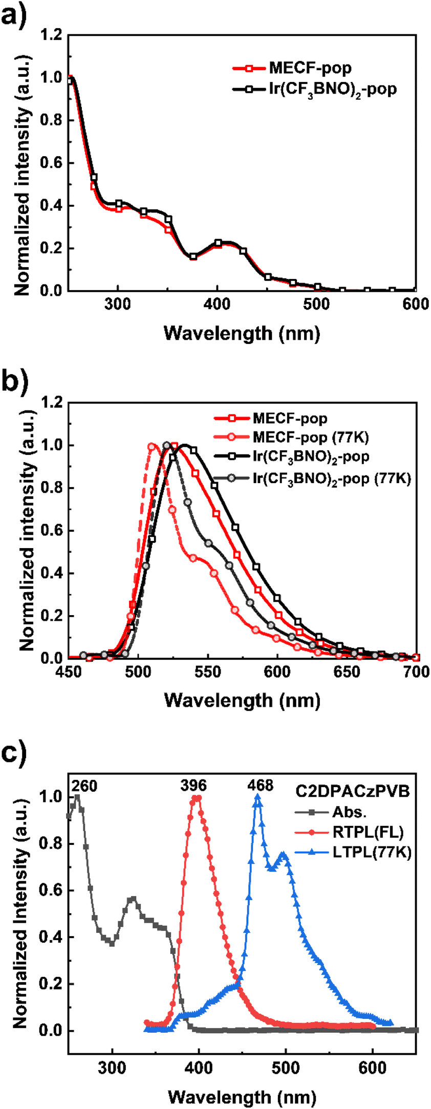 | ||
| Fig. 1 (a) UV-vis absorption, (b) PL spectra of MECF-pop and Ir(CF3BNO)2-pop. (c) UV-vis absorption, RTPL (FL) and LTPL (Ph) spectra of C2DPACzPVB. | ||
| Compound | Tg/Td (°C) | λPL (nm) | λPLd (nm) | PLQYe (%) | τPL (μs) | HOMOf (eV) | LUMOg (eV) | Eg (eV) | ET (eV) | FWHM (nm) | |||
|---|---|---|---|---|---|---|---|---|---|---|---|---|---|
| CH2Cl2a | Tolb | PMMAc | Neat film | 77 K | CH2Cl2 | PMMAc | |||||||
| a Measured in degassed CH2Cl2 solution at RT (1 × 10⁻⁵ M).b Measured in degassed toluene solution at RT (1 × 10⁻⁵ M).c Measured PMMA film with a 5 wt% Ir complex.d Measured in 2-MeTHF solution at 77 K (1 × 10⁻⁵ M).e Relative PLQYs of Ir(III) complexes.f Determined from UPS.g Determined by adding up the optical band and the HOMO value. | |||||||||||||
| MECF-pop | 153/407 | 525 | 522 | 519 | 534 | 512 | 95 | 1.52 | −5.46 | −3.01 | 2.45 | 2.42 | 63 |
| Ir(CF3BNO)2-pop | 139/413 | 533 | 526 | — | 554 | 522 | 90 | 1.78 | −5.62 | −3.22 | 2.40 | 2.38 | 72 |
| C2DPACzPVB | —/360 | 396 | — | — | — | 468 | — | — | −5.35 | −2.14 | 3.21 | 2.65 | — |
To determine the distribution of HOMO and LUMO for MECF-pop and C2DPACzPVB, density functional theory calculations were performed with B3LYP/6-31G(d,p) for light elements (H, C, N, O, and F) and B3LYP/LANL2DZ for Ir as the basis sets (Fig. S12 and S13†). The HOMO of MECF-pop was mainly dispersed on Ir center and ancillary ligand, while electron distribution of LUMO was dominated at the main ligand. We assume that the electron-donating methyl group at the para position of pyridine affects the LUMO energy level. Thermal properties of MECF-pop and C2DPACzPVB were investigated by thermogravimetric analysis (TGA) and differential scanning calorimetry (DSC). The decomposition temperature (Td) and glass transition temperature (Tg) of MECF-pop determined from TGA and DSC were found to be 407 °C and 153 °C, respectively (Fig. S14† and Table 1). DSC and TGA thermograms of C2DPACzPVB are shown in Fig. S15.† The crosslinking behavior of C2DPACzPVB film was assessed through solvent resistance measured by UV-vis spectroscopy. The optimum cross-linking temperature was found to be 200 °C (Fig. S16†).
The transient PL decays (τ) of MECF-pop and Ir(CF3BNO)2-pop films (5 wt% in PMMA) were measured at room-temperature. As shown in Fig. S17,† the exciton lifetime (τ) of both emitters were collected from mono-exponential fitting because the emitters indicated mono-exponential decay. The MECF-pop has a shorter exciton lifetime of 1.5 μs than 1.8 μs of Ir(CF3BNO)2-pop. Moreover, to extract radiative decay rate (kr) and non-radiative decay rate (knr) of both emitters, we measured relative photoluminescence quantum yields (ΦPL) of Ir(CF3BNO)2-pop and MECF-pop in N2-saturated DCM, with relative ΦPL = 90 and 95% (compared with ΦPL of fac-Ir(ppy)3),39 respectively. The ratios of kr/knr (kr = ΦPL/τ and knr = (1 − ΦPL)/τ; ref. 40) of MECF-pop and Ir(CF3BNO)2-pop are calculated to be 6.3/0.3 and 5.0/0.6 × 105 s−1, respectively. Accordingly, the MECF-pop has a higher potential for green PHOLED than Ir(CF3BNO)2-pop.
To evaluate the electroluminescence (EL) of MECF-pop, we fabricated PHOLEDs with the configuration: indium tin oxide (ITO) on glass/poly(3,4-ethylenedioxythiophene):polystyrene sulfonic acid (PEDOT:PSS)/emissive layer (EML)/TPBi/lithium fluoride (LiF)/aluminum (Al). The EML solution (1 wt% dissolved in CB) was prepared (detailed description of EML solution is described in ESI†). The PEDOT:PSS and EML films were formed by spin-coating (wet-process) by dissolving PEDOT:PSS in water with 3000 rpm and the EML materials in CB with 1000 rpm (Device A), while the TPBi, LiF, and Al were deposited via thermal evaporation (dry-process) (Fig. 2a). As shown in Fig. 2, the PHOLED using a chlorinated solvent of CB showed impressive device performance. The optimized PHOLED exhibited an EQEmax of 26.4%, a CEmax of 94.8 cd A−1, and a PEmax of 42.5 lm W−1. Furthermore, a high brightness of 23![[thin space (1/6-em)]](https://www.rsc.org/images/entities/char_2009.gif) 404 cd m−2 and a narrow FWHM of 72 nm were observed. Importantly, the MECF-pop indicated higher device performance than Ir(CF3BNO)2-pop in the same device architecture, presumably because the MECF-pop has higher kr and lower knr than Ir(CF3BNO)2-pop as mentioned above.
404 cd m−2 and a narrow FWHM of 72 nm were observed. Importantly, the MECF-pop indicated higher device performance than Ir(CF3BNO)2-pop in the same device architecture, presumably because the MECF-pop has higher kr and lower knr than Ir(CF3BNO)2-pop as mentioned above.
 | ||
| Fig. 2 (a) Energy level diagram of solution-processed PHOLEDs. (b) Molecular structure of TCTA, TPBi, and MECF-pop, (c) J–V–L curve, (d) EL spectra, (e) EQE–L curve, and (f) CE–L–PE curve of Devices A–D. | ||
Additionally, we fabricated eco-friendly solution-processed green PHOLEDs using 2-MA (Device B and C). As depicted in Fig. 2, Device B/C exhibited EQEmaxs of 16.8/20.2% and CEmaxs of 61.0/73.7 cd A−1, respectively. Surprisingly, Device B and C had lower device performance compared to Device A, despite sharing the same device architecture as well as the same EML formation conditions, i.e. spin-coating at 1000 rpm and a 1 wt% concentration of EML solution. To understand the origin of the reduced device performance of Device B and Device C compared to that of Device A, we analyzed the EML thicknesses according to solvents. To evaluate film thicknesses, we utilized alpha-step for thick films and Beer–Lambert law for thin films. First, we compared the thickness between an EML and a TPBi film under the same conditions (formed by 1 wt% dissolved in CB and 500 rpm in N2 atmosphere) using alpha-step. The EML and TPBi films showed similar thicknesses (Table S2†). To estimate EML thicknesses, we utilized TPBi films to exclude bimolecular interactions between TCTA and TPBi. The absorption coefficient of TPBi film was found to be 9603 × 10−2 cm−1 (@307 nm) using Beer–Lambert law (Fig. S18†). Based on the information from alpha-step measurement and the absorption coefficient, the thickness of TPBi films were calculated. TPBi films formed by CB indicated relatively thicker thickness than TPBi films formed by 2-MA. The estimated film thicknesses of EMLs are 40, 28, and 25 nm for Devices A, B, and C, respectively (Table S2†). Despite using the same concentration and spin-coating conditions, the resulting different film thicknesses might be attributed to the intrinsic physical property difference between CB and 2-MA. 2-MA has a higher boiling point and a lower solution viscosity than CB. Therefore, the film thicknesses of Device B and C are thinner than that of Device A. The thinner EML causes the occupied exciton generation zone on the electron transport layer (ETL) and/or HTL, which induces the quenched exciton through non-radiative pathways at the interfaces, ETL, and HTL.
It should be noted that Device C showed a slightly better device performance compared to Device B, although it was fabricated under air conditions and had similar EML thickness. To understand the difference in performance between Device B and C despite having comparable EML thicknesses, we investigated the dependence of exciplex formation in the EML on the processing solvents and spin-coating atmosphere using PL and time-of-flight secondary ion mass spectrometry (ToF-SIMS). We also measured absolute ΦPL and charge carrier mobilities of EML films under different film-forming conditions. Fig. 3a shows the PL properties of TCTA, TPBi, and mixed TCTA:TPBi films formed by 2-MA solution as well as the higher performance giving CB solution. The mixed TCTA:TPBi film, formed by 1000 rpm and 2-MA in the N2-filled glove box, exhibited the combined emission from TCTA, TPBi, and the exciplex (a bimolecular transition from an electronically excited molecule to another molecule in the ground state). Interestingly, the mixed TCTA:TPBi film, formed by 1000 rpm and 2-MA in air, had a higher ratio of exciplex than that formed by formed by 1000 rpm and 2-MA in N2. We also found that 2-MA solution spin-coated at 500 rpm in glovebox generated nearly the same PL spectrum as that from 2-MA solution spin-coated at 1000 rpm in air. In contrast, the mixed TCTA:TPBi film formed by CB exhibited the complete disappearance of the PL emission peaks of TCTA and TPBi, with the appearance of an exciplex PL peak only. We hypothesized that the mixed TCTA:TPBi film prepared using 2-MA induced substantial un-uniform distribution of each host material. To estimate the PLQYs depending on exciplex formation, absolute PLQYs under various EML conditions were measured. The EML processed from CB has a high absolute ΦPL of 96.6%. Interestingly, for the EML films formed by 2-MA, the absolute ΦPL of EML films were enhanced according to the increased exciplex ratio (Fig. 2a and Table S3†). These results indicate a direct correlation between PLQY and the proportion of exciplex. In other words, the exciplex formation is beneficial to achieve higher EQEs.
 | ||
| Fig. 3 (a) PL properties of TCTA, TPBi, and mixed films (TCTA and TPBi). (b) Hole mobility of mixed films depending on film forming conditions using CB and 2-MA. ToF-SIMS 3D analysis of (c) TCTA (C54H37N+), (d) TPBi (C45H21N6+), and (e) mixed TCTA and TPBi distribution according to film forming conditions. | ||
The exciplex formation is correlated with nano-scale morphology in EMLs that was revealed using ToF-SIMS. (Note that atomic force microscopy (AFM) images were taken, but they did not present notable differences (Fig. S19†)) Positive ion images for TCTA molecule (C54H37N4)+ and TPBi (C45H31N6)+ from the TCTA:TPBi films, which were prepared under the conditions of Devices A-D, are shown in Fig. 3c–e. The TCTA:TPBi films formed by using CB (1000 rpm in N2 atmosphere) and formed by using 2-MA (1000 rpm in air atmosphere and 500 rpm in N2 atmosphere) exhibited a well-distributed population of TCTA and TPBi molecules. In contrast, the TCTA:TPBi film prepared using 2-MA (1000 rpm in N2 atmosphere) exhibited highly aggregated TCTAs. Interestingly, the TCTA:TPBi film formed in N2 with a decreased spin coating RPM (from 1000 rpm to 500 rpm in the glovebox) indicated the relatively evenly distributed population of TCTA and TPBi molecules. Therefore, the TCTA:TPBi film formed by 500 rpm and 2-MA in the glovebox has optimized nano-scale morphology, which indicated the highest absolute ΦPL of EML film using green solvent. The results indicate that the evenly well-distribution of comprising host molecules is key to obtaining high device performance.
To estimate charge carrier mobility depending on nano-scale morphology, the hole mobilities of mixed films were investigated using space-charge-limited current (SCLC) (Fig. 3b). The energy level diagram of the hole-only device components is shown in Fig. S20.† The hole mobility of mixed film formed by CB (1000 rpm in N2 atmosphere), 2-MA (1000 rpm in Air), and 2-MA (500 rpm in N2 atmosphere) was 1.9 × 10⁻⁷, 1.5 × 10⁻⁷, and 1.7 × 10⁻⁷ cm2 V−1 s−1 at 1000 V1/2 cm−1/2, respectively. Furthermore, the hole mobility of the mixed film using 2-MA (1000 rpm in N2 atmosphere) was much lower than the other mixed films due to the disproportionate distribution of TCTA. These results suggest that the disproportionate distribution of host materials led to a decrease in hole mobility, as hole transport through TCTA molecules was hindered by the increased distances between molecules. This disproportionate distribution of TCTA or TPBi resulted in alterations to the electron/hole transport properties and energy transfer dynamics within the EML.
Nevertheless, the performance of Device C is still lower than that of Device A. That is, Device A and C showed a difference of EQE over 20% despite only a 10% difference in PLQY. The reason for this unexpected difference is still occupied exciton generation zone on HTL and/or ETL. To overcome the problem mentioned above, we conducted optimization of thickness and nano-scale morphology of EML (500 rpm in N2 atmosphere, Device D). However, Device D has still lower device performance than Device A, even though Device D has a slightly improved device performance compared with Device C (Fig. 2 and Table 2). To optimize eco-friendly PHOLEDs, we utilized C2DPACzPVB as newly developed thermally cross-linkable HTL and 1,3,5-tris(3-pyridyl-3-phenyl)benzene (TmPyPB) as ETL to reduced non-radiative pathway via HTL, ETL, and interfaces. We fabricated Device E with the architecture: PEDOT:PSS/C2DPACzPVB/optimized EML/TmPyPB/LiF/Al (Fig. 4a). The optimized Device E showed an EQEmax of 22.7%, a CEmax of 81.2 cd A−1, and a PEmax of 42.5 lm/W with a maximum luminance of 16067 cd m−2 (Fig. 4b–d). The deep HOMO energy of TmPyPB blocked a leakage of the hole.41 A C2DPACzPVB which has a high triplet energy level (2.65 eV) and shallow LUMO energy level (−2.14 eV) suppressed energy transfer and electron leakage from EML to HTL, respectively. Furthermore, the suitable HOMO energy level of C2DPACzPVB induced the decrease of turn-on voltage due to efficient hole injection. Therefore, Device E showed improved device performance as compared to Device D.
| Device | Spin-coating condition (thickness) | Environment | Solvent | Von (V) | EQE (%) | CE (cd A−1) | PE (lm W−1) | CIE (x,y) | ELmax (nm) | Lmax (cd m−2) | |||||
|---|---|---|---|---|---|---|---|---|---|---|---|---|---|---|---|
| Max., @1000 cd m−2 | @10 mA cm−2 | ||||||||||||||
| a Operation voltage (OV) at 1 cd m−2.b OV at 1000 cd m−2. | |||||||||||||||
| A | 1000 rpm (40 nm) | N2 | CB | 5.0a | 7.4b | 26.4 | 23.5 | 94.8 | 83.3 | 42.5 | 35.5 | 0.340 | 0.616 | 523 | 23404 |
| B | 1000 rpm (28 nm) | N2 | 2-MA | 5.2a | 7.2b | 16.8 | 12.8 | 61.0 | 45.7 | 32.0 | 19.8 | 0.329 | 0.620 | 522 | 5500 |
| C | 1000 rpm (25 nm) | Air | 2-MA | 4.3a | 6.1b | 20.2 | 14.9 | 73.7 | 53.9 | 46.3 | 28.2 | 0.327 | 0.618 | 522 | 15345 |
| D | 500 rpm (32 nm) | N2 | 2-MA | 5.5a | 7.6b | 21.7 | 20.2 | 78.3 | 73.2 | 35.1 | 27.7 | 0.341 | 0.611 | 522 | 17908 |
| E | 500 rpm (32 nm) | N2 | 2-MA | 3.9a | 6.8b | 22.7 | 21.8 | 81.2 | 78.2 | 42.5 | 36.4 | 0.338 | 0.614 | 522 | 16067 |
 | ||
| Fig. 4 (a) Energy level diagram of Device E and molecular structure of C2DPACzPVB. (b) J–V–L curves. (c) EL spectrum. (d) EQE–L curve. (e) CE–L–PE curves of Device E. | ||
Conclusion
In summary, we designed and synthesized a novel green emitting Ir(III) complex, MECF-pop, and a new thermally cross-linkable HTL material, C2DPACzPVB for s-PHOLEDs. The phosphorescent emitter showed pure green emission, good thermal properties, PLQY, and FWHM. To evaluate the potential of the new emitter and HTL material, we fabricated s-PHOLEDs using MECF-pop in CB and an environmentally friendly solvent, 2-MA, used as a food additive. Impressively, the CB-processed optimized device exhibited an EQEmax of 26% with a CEmax of 95.5 cd m−2. To fabricate the eco-friendly s-PHOLEDs, we introduced C2DPACzPVB as a hole transport material and 2-MA as a food additive solvent. The optimized eco-friendly s-PHOLED exhibited an EQEmax of 22.7% and a CEmax of 81.2 cd A−1 with pure green emission. Although 2-MA well dissolved the EML materials (i.e. MECF-pop, TPBi, and TCTA), the eco-friendly s-PHOLEDs fabricated showed lower device performance than the s-PHOLEDs using CB solvent because EMLs formed by 2-MA solution do not possess proper nanoscale morphology to form exciplex. In other words, the nanoscale morphology in EML film is a crucial factor in improving PLQY and affecting charge carrier mobility. To improve eco-friendly s-PHOLEDs, film thickness, nanoscale morphology, and carrier mobility were considered depending on solvents. We strongly believe that our results will assist researchers in achieving high-performance eco-friendly s-PHOLEDs.Data availability
The data supporting this article have been included as part of the ESI.†Author contributions
Dr H.-Y. Park, Dr S. Ameen, and T. Manigandan: conceptualization, data curation, formal analysis, and writing- original draft; Dr R. Kumaresan: data curation and writing – review and editing; H. Kim, J. Park, D. Song, M. J. Jeon, J. Lee, Dr J. S. Jin, G. Kim, and Dr M. K. Song: investigation and formal analysis; Dr J.-S. Jee: conceptualization and writing – review and editing; Prof. B. Kim and Prof. S.-H. Jin: supervision, conceptualization, and writing – review and editing.Conflicts of interest
There are no conflicts to declare.Acknowledgements
H.-Y. Park, S. Ameen, and T. Manigandan contributed equally to this work. The research received support from the Technology Innovation Program (20016283) funded by the Ministry of Trade, Industry & Energy (MOTIE, Korea), as well as from the Basic Science Research Program through the National Research Foundation of korea (NRF) grants funded by the Ministry of Education (NRF-2022R1A6A3A01086432). Additionally, support was provided by the Korea Basic Science Institute under the R&D program (Project No. C330430) and NRF under project number NRF-2023R1A2C3006550 supervised by the Ministry of Science and ICT. Furthermore, this research is backed by a grant from the NRF under project number RS-2023-00244309, funded by the Ministry of Science, ICT, and Future Planning.References
- C. W. Tang and S. A. Vanslyke, Appl. Phys. Lett., 1987, 51, 913–915 CrossRef CAS.
- G. Hong, X. Gan, C. Leonhardt, Z. Zhang, J. Seibert, J. M. Busch and S. Bräse, Adv. Mater., 2021, 33, 2005630 CrossRef CAS PubMed.
- M. A. Baldo, D. F. O'Brien, Y. You, A. Ahoustikov, S. Sibely, M. E. Thompson and S. R. Forrest, Nature, 1998, 395, 151–154 CrossRef CAS.
- M. A. Baldo, S. Lamansky, P. E. Burrow, M. E. Thompson and S. R. Forrest, Appl. Phys. Lett., 1999, 75, 4–6 CrossRef CAS.
- K. H. Kim, S. Lee, C. K. Moon, S. Y. Kim, Y. S. Park, J. H. Lee, J. Woo Lee, J. Huh, Y. You and J. J. Kim, Nat. Commun., 2014, 5, 4769 CrossRef CAS PubMed.
- D. Zhang, J. Qiao, D. Zhang and L. Duan, Adv. Mater., 2017, 29, 1702847 CrossRef PubMed.
- H.-Y. Park, A. Maheshwaran, C.-K. Moon, H. Lee, S. S. Reddy, V. G. Sree, J. Yoon, J. W. Kim, J. H. Kwon, J.-J. Kim and S.-H. Jin, Adv. Mater., 2020, 2002120 CrossRef CAS PubMed.
- J. Sun, H. Ahn, S. Kang, S.-B. Ko, D. Song, H. A. Um, S. Kim, Y. Lee, P. Jeon, S.-H. Hwang, Y. You, C. Chu and S. Kim, Nat. Photon., 2022, 16, 212–218 CrossRef CAS.
- L. Duan, L. Hou, T.-W. Lee, J. Qiao, D. Zhang, G. Dong, L. Wang and Y. Qiu, J. Mater. Chem., 2010, 20, 6392–6407 RSC.
- M. Shibata, Y. Sakai and D. Yokoyama, J. Mater. Chem. C, 2015, 3, 11178–11191 RSC.
- W. R. Mateker, T. Heumueller, R. Cheacharoen, I. T. Sachs-Quintana, M. D. McGehee, J. Warnan, P. M. Beaujuge, X. Liu and G. C. Bazan, Chem. Meter., 2015, 27, 6345–6253 CrossRef CAS.
- T.-W. Lee, T. Noh, H.-W. Shin, O. Kwon, J.-J. Park, B.-Ki. Choi, M.-S. Kim, D. W. Shin and Y.-R. Kim, Adv. Funct. Mater., 2009, 19, 1625–1630 CrossRef CAS.
- V. N. Hamanaka, E. Salsberg, F. J. Fonseca and H. Aziz, Org. Electron., 2020, 78, 105509 CrossRef CAS.
- Y. J. Cho, Y. Zhang, H. Yu and H. Aziz, Adv. Funct. Mater., 2016, 26, 8662–8669 CrossRef CAS.
- V. G. Sree, H.-Y. Park, W. Cho and S.-H. Jin, Mol. Cryst. Liq. Cryst., 2017, 654, 73–82 CrossRef CAS.
- W. Cho, G. Sarada, A. Maheshwaran, Y. Nam, J. Y. Lee and S.-H. Jin, J. Mater. Chem. C, 2017, 5, 10029–10038 RSC.
- G. Sarada, W. Cho, A. Maheshwaran, H.-Y. Park, Y.-S. Gal, M. Song and S.-H. Jin, Adv. Funct. Mater., 2017, 27, 1701002 CrossRef.
- M.-Ju. Tsai, W.-W. Huang, L.-M. Chen, G.-L. Ruan, D. Luo, Z.-L. Tseng and K.-T. Wong, J. Mater. Chem. C, 2023, 11, 1056–1066 RSC.
- V. G. Sree, A. Maheshwaran, H. Kim, H.-Y. Park, Y. Kim, J. C. Lee, M. Song and S.-H. Jin, Adv. Funct. Mater., 2018, 28, 1804714 CrossRef.
- R. Kumaresan, H.-Y. Park, A. Maheshwaran, H. Park, Y. Do, M. Song, J. Yoon, S. I. Ahn and S.-H. Jin, Adv. Optical Mater., 2022, 10, 2101686 CrossRef CAS.
- J. Hu, Y. Wang, Q. Li, S. Shao, L. Wang, X. Jing and F. Wang, Chem. Sci., 2021, 12, 13083 RSC.
- T.-H. Han, M.-R. Choi, C.-W. Jeon, Y.-H. Kim, S.-K. Kwon and T.-W. Lee, Sci. Adv., 2016, 2, 21601428 Search PubMed.
- N. Aizawa, Y.-J. Pu, M. Watanabe, T. Chilba, K. Ideta, N. Toyota, M. Lgarashi, Y. Suzuri, H. Sasabe and J. Kido, Nat. Commund., 2014, 5, 5756 CrossRef PubMed.
- R. Kumaresan, A. Maheshwaran, H.-Y. Park, K. Sung, J. Choi, W. Cho, M. Song, S. I. Ahn and S.-H. Jin, J. Mater. Chem. C, 2020, 8, 12959–12967 RSC.
- V. G. Sree, C. Bathula, A. N. Kadam, M. Ravindra, K. M. Mahadevan, J. I. Sohn, H.-S. Kim and H. Im, Nano Energy, 2022, 92, 106753 CrossRef CAS.
- S. K. Podapangi, F. Jafarzadeh, S. Mattiello, T. G. Korukonda, A. Singh, L. Beverina and T. M. Brown, RSC Adv., 2023, 13, 18165 RSC.
- J. Lee, S. A. Park, S. U. Ryu, D. Chung, T. Park and S. Y. Son, J. Mater. Chem. A, 2020, 8, 21455–21473 RSC.
- N. P. Holmes, H. Munday, M. G. Barr, L. Thomesen, M. A. Marcus, A. L. D. Kicoyne, A. Fahy, J. V. Stam, P. C. Dastoor and E. Moons, Green Chem., 2019, 21, 5090–5103 RSC.
- J. Lee, M. M. Byranvand, G. Kang, S. Y. Son, S. Song, G.-W. Kim and T. Park, J. Am. Chem. Soc., 2017, 139, 12175–12181 CrossRef CAS PubMed.
- Z. Ma, B. Zhao, Y. Gong, J. Deng and Z. Tan, J. Mater. Chem. A, 2019, 7, 22826–22847 RSC.
- J. Lee, J. W. Kim, S. A. Park, S. Y. Son, K. Choi, W. Lee, M. Kim, J. Y. Kim and T. Park, Adv. Energy Mater., 2019, 9, 1901829 CrossRef.
- K. Zhang, Z. Chen, A. Armin, S. Dong, R. Xia, H.-L. Yip, S. Shoaee, F. Huang and Y. Cao, Sol. RRL, 2018, 2, 1700169 CrossRef.
- S. Y. Son, J. W. Kim, J. Lee, G.-W. Kim, J. Hong, J. Y. Kim and T. Park, J. Mater. Chem. A, 2018, 6, 24580–24587 RSC.
- J. Lee, T. H. Lee, M. M. Byranvand, K. Choi, H. I. Kim, S. A. Park, J. Y. Kim and T. Park, J. Mater. Chem. A, 2018, 6, 5538–5543 RSC.
- H. Zhamg, H. Yao, W. Zhao, L. Ye and J. Hou, Adv. Energy Mater., 2016, 6, 1502177 CrossRef.
- X. Du, X. Lu, J. Zhao, Y. Zhang, X. Li, H. Lin, C. Zheng and S. Tao, Adv. Funct. Mater., 2019, 29, 1902078 CrossRef.
- H.-Y. Park, S. Ameen, R. Kumaresan, J. Lee, J. Park, D. Song, J. Lee, Y. Heo, B. Kim and S.-H. Jin, Adv. Optical Mater., 2023, 11, 2202641 CrossRef CAS.
- J. Lee, H.-F. Chen, T. Batagoda, C. Coburn, P. I. Djurovich, M. E. Thompson and S. R. Forrest, Nat. Mater., 2016, 15, 92 CrossRef CAS PubMed.
- C.-C. Wang, Y.-M. Jing, T.-Y. Li, Q.-L. Xu, S. Zhang, W.-N. Li, Y.-X. Zheng, J.-L. Zuo, X.-Z. You and X.-Q. Wang, Eur. J. Inorg. Chem., 2013, 33, 5683 CrossRef.
- A. B. Tamayo, B. D. Alleyne, P. I. Djurovich, S. Lamansky, I. Tsyba, N. N. Ho, R. Bau and M. E. Thompson, J. Am. Chem. Soc., 2023, 125, 7377–7387 CrossRef PubMed.
- A. Maheswaran, R. Kumaresan, H.-Y. Park, J. kim, H. Kim and S.-H. Jin, Org. Electron., 2022, 106, 106517 CrossRef CAS.
Footnote |
| † Electronic supplementary information (ESI) available. See DOI: https://doi.org/10.1039/d4ra08598a |
| This journal is © The Royal Society of Chemistry 2025 |