
 Open Access Article
 This Open Access Article is licensed under a Creative Commons Attribution-Non Commercial 3.0 Unported Licence
Optimizing Cs2CuBiBr6 double halide perovskite for solar applications: the role of electron transport layers in SCAPS-1D simulations
Khandoker Isfaque Ferdous Utshoa,
S. M. G. Mostafaa,
Md. Tarekuzzaman ab,
Muneera S. M. Al-Saleemc,
Nazmul Islam Nahidab,
Jehan Y. Al-Humaidic,
Md. Rasheduzzamanab,
Mohammed M. Rahman*d and
Md. Zahid Hasan*ab
ab,
Muneera S. M. Al-Saleemc,
Nazmul Islam Nahidab,
Jehan Y. Al-Humaidic,
Md. Rasheduzzamanab,
Mohammed M. Rahman*d and
Md. Zahid Hasan*ab
aDepartment of Electrical and Electronic Engineering, International Islamic University Chittagong, Kumira, Chittagong, 4318, Bangladesh. E-mail: zahidhasan.02@gmail.com
bMaterials Research and Simulation Lab, Department of Electrical and Electronic Engineering, International Islamic University Chittagong, Kumira, Chittagong, 4318, Bangladesh
cDepartment of Chemistry, Science College, Princess Nourah bint Abdulrahman University, P.O. Box 84428, Riyadh 11671, Saudi Arabia
dCenter of Excellence for Advanced Materials Research (CEAMR) & Chemistry Department, King Abdulaziz University, Jeddah 21589, Saudi Arabia. E-mail: mmrahman@kau.edu.sa
First published on 23rd January 2025
Abstract
Perovskite solar cells are commonly employed in photovoltaic systems because of their special characteristics. Perovskite solar cells remain efficient, but lead-based absorbers are dangerous, restricting their manufacture. Therefore, studies in the field of perovskite materials are now focusing on investigating lead-free perovskites. The SCAPS-1D simulator is used to simulate the impact of lead-free double perovskite as the absorber in perovskite solar cells. The research examines how the effectiveness of solar cells is impacted by a hole transport layer (CBTS) and several electron transports layers (WS2, C60, PCBM, and TiO2), using Ni and Al acting as the back and front contacts metal. This work explores the impact of a Cs2CuBiBr6 perovskite as a solar cell absorber. The effectiveness of these device structures depends on defect density, absorber thickness, ETL thickness, and ETL combination. With WS2, C60, PCBM, and TiO2, the device's power conversion efficiency (PCE) is 19.70%, 18.69%, 19.52%, and 19.65%, respectively. This research also highlights the impact of the absorber and HTL thickness. This investigation further included the analysis of the valence band offset (VBO) and conduction band offset (CBO). We also investigated the current density–voltage (J–V), quantum efficiency (QE), series and shunt resistance, capacitance-Mott–Schottky characteristics, and photocarrier generation–recombination rates and effective temperature. This study provides crucial structural design guidelines for a lead-free double perovskite device and highlights solar energy optoelectronic developments.
1. Introduction
With the potential to significantly influence human society and mold the future of renewable energy, solar cells represent a promising technological advancement. Sustainable energy is a plentiful resource that emits no carbon dioxide, is free to use, and is freely available.1,2 Photovoltaic cells use visible light to generate power by converting solar photons to electric energy.3,4 In the last two decades, significant technological advancements in photovoltaic technology have driven substantial cost reductions and remarkable improvements in the PCE of PV cells. The exploration and application of innovative materials present exciting possibilities for even greater advancements in the years to come.5,6 There are three generations of photovoltaic cell technology. In 1954, Bell Laboratories produced the first generation, with an efficiency of 6%. Second-generation solar cells, also called thin-film photovoltaic cells, offer a more affordable option than conventional silicon wafer-based cells. These thin-film cells have clear benefits in terms of material efficiency and lower total mass. They are distinguished by their flexibility and lightweight construction.3,7 Third-generation solar cells have improved dependability and efficiency compared to previous versions. The exceptional efficiency of these cells is due to their diversified composition, particularly including conductive polymers, organic dyes, silicon nanowires, and nanomaterials with large band gaps.8–10The SCAPS-1D simulator has been utilized by researchers for numerical simulations, utilizing computational analysis to support cost-effective production processes and optimize solar cell design. Before a device is put into production, it can be thoroughly evaluated in a virtual environment using simulation tools, which can save a lot of resources and time.11 The SCAPS 1D simulation program facilitates the exploration and linkage of experimental as well as theoretical studies. Previously, planar FA-based PSCs were analyzed and their performance was illustrated using both numerical simulations and experimental analysis.12 More than ever, the necessity of alternative energy sources is highlighted by the world's expanding energy demand, the increasing exhaustion of fossil fuel resources, and the rising levels of pollution that feed global warming.13–15 Renewable energy is becoming increasingly acknowledged as a vital source of electricity because of the worldwide problem of global warming. Especially remarkable is solar power, which is the most abundant energy resource on the planet. The high initial prices and low conversion efficiency of solar power generation remain barriers to mainstream adoption. It is anticipated that advancements in perovskite-based solar cell structure will increase production capacity while lowering resource and energy consumption.16,17 The key factors driving perovskite film photovoltaics' growing popularity are their ability to produce them quickly and effectively, as well as the low material requirements and resulting cost reductions.6,18–20
The perovskite material, such as lead-free double perovskite structure Cs2B′B′′Br6 where B′ = Cu and B′′ = Bi. This perovskite structure is a lead-free non-toxic substance with preferred absorption.21 Increased charge carrier production, a higher rate of photon generation, resulting in reduced energy loss and an enhanced concentration of electric charge carriers at the electrodes.22,23 In comparison to conventional bismuth-based double perovskite solar cells, Cesium Copper Bismuth Bromide (Cs2CuBiBr6), referred to as the absorber, demonstrates enhanced thermal stability, owing to its single crystal structure and lower susceptibility to moisture. When compared to CH3NH3PbX3, McClure and coworkers observed that Cs2AgBiBr6 and Cs2AgBiCl6 had a superior bandgap and good stability.24 Cs2AgBiBr6 and Cs2AgBiCl6 exhibit poor efficiency due to high charge carrier effective masses, insufficient charge carrier transport properties, and large band gaps (>2 eV),25–27 making them unsuitable for solar cell applications. Conversely, compared to Cs2AgBiBr6 and Cs2AgBiCl6, the Cs2CuBiBr6 absorber demonstrated an ideal band gap (1.24 eV), larger light absorption abilities, and superior performance, making it appropriate for the PSC.21,28,29 Due to its substantial bandgap, which is closely correlated with VOC, the inclusion of bromide in the perovskite might facilitate a high VOC. In addition to the preferred optical band gap and light spectrum, their strength under illumination in humid conditions, and elevated temperatures are markedly enhanced in comparison to organic lead halide perovskites.30 In PSCs, utilizing an appropriate electron transport layer (ETL) and a hole transport layer (HTL) can improve the absorber's performance and efficiency. A light-absorbing perovskite layer is often positioned between the ETL and the HTL in mesoporous and planar structures, which are common in solar cell systems. Electrons can move between mesoscopic perovskite structures and nanoparticles of mesoporous metal oxides like TiO2 (ref. 31 and 32) and ZnO33 through the ETL, while holes can successfully transmit through HTLs.34 The thickness of the ETL, HTL, absorber layer, as well as their interface and phase matching characteristics, are the main determinants of photovoltaic parameters such as the open-circuit voltage (VOC), short-circuit current density (JSC), fill factor (FF), and power conversion efficiency (PCE). Several semiconductor materials have been used as ETLs, including ZnO, TiO2, WO3, I2O3, WS2, PCBM, C60, Al2O3, and SnO2.35–38 Prior research has not extensively investigated the usage of ETLs like WS2, PCBM, and CdS in combination with Cs2CuBiBr6 perovskite-based solar cells.21 The ETL used in this work comprises Tungsten Disulfide (WS2), Buckminsterfullerene (C60), phenyl-C61 butyric acid methyl ester (PCBM), and Titanium Dioxide (TiO2) as the electron transport materials. The electron transport layer made of tungsten disulfide (WS2) is very desirable in optoelectronics because of its adaptability and excellent bandgap.39,40 Furthermore, the effective extraction of electrons has been observed by organic electron transport layers, such as C60, when combined with the perovskite layers.41 The need for high-temperature heating of TiO2 to attain the rutile form for solar application, along with the confined movement of electrons, impedes its effectiveness as an electron transport material in PSCs.31,42–44 The PCBM ETL obviates the necessity for thermal annealing or processing at high temperatures, therefore considerably streamlining the production procedure and reducing production costs.
Moreover, the HTL and nearby surfaces affect the solar cell's efficiency, durability, and manufacturing cost.45,46 Solar cell performance is improved by small-molecule HTLs; however, they don't have enough photostability and thermal stability. By comparison, polymeric HTLs are attractive because they are suitable with other materials, water-repellent, and can withstand high temperatures.47 But these HTLs could have limitations with their optoelectronic characteristics, which might lead to lower efficiency. Due to the increasing demand for affordable solar cell manufacturing, earth-abundant, air-stable thin-film materials like copper barium thiocyanate (CBTS) are being investigated as possible substitutes for widely used HTLs like Cu2O, CuSCN, CuSbS2, NiO, P3HT, PEDOT: PSS, spiro-OMeTAD, CuI, CuO, and V2O5. CBTS is an appropriate option for HTL application due to its large atomic size, non-centrosymmetric crystal structure, high absorption coefficient, variable bandgap, and effective light-absorbing properties.47–50 The shallow valence band of CBTS aligns well with Cs2B′B′′Br6, leading to modest energy loss when CBTS is used as the hole transport layer in Cs2B′B′′Br6 (where B′ = Cu and B′′ = Bi) based PSCs. Prior research has shown that the CBTS HTL had favorable characteristics due to its suitable absorption coefficient and electron affinity.51
Therefore, ETL and HTL are implemented to improve the PV parameters of solar cells. Furthermore, this investigation on Cs2CuBiBr6 has shown substantial advancement, increasing efficiency from the previous 14.08% to an improved 19.70%. The energy band alignment was likely enhanced by the use of CBTS as a hole transport layer (HTL) and Ni as the back-contact metal, which decreased energy losses during charge carrier transport. This ideal alignment improves charge extraction and minimizes recombination. The use of ITO instead of FTO may have enhanced optical transmittance and electrical conductivity. Thus, more photons are able to reach the active perovskite layer, which improves the production of charge carriers. These results highlight the significant advancements attained in our study, which boost the performance of the examined absorber materials. Utilizing SCAPS-1D software to investigate single absorber-based perovskite solar cells enhances experimental efficiency by virtually adjusting device settings. SCAPS-1D determines optimal designs and material selections by simulating many combinations, thus assisting experimentalists in the fabrication of high-performance devices.
This process expedites development, ensuring more efficient and accurate manufacturing procedures, eventually resulting in improved device performance. Therefore, this investigation entails the assessment of Cs2CuBiBr6 in a variety of configurations, such as WS2, C60, PCBM, and TiO2 as electron transport layers (ETL), CBTS as hole transport layers (HTL), Al as the front contact metal, and Ni as the back-contact metal. The photovoltaic (PV) performance is investigated and evaluated by observing the impact of variations in the absorber thickness and ETL thickness, as well as the impact of series and shunt resistance on PV parameters, to determine the optimal configurations. To further understand the studied SC designs, we also compute the current–voltage (J–V) curves, capacitance–voltage (C–V) properties, quantum efficiency (QE), generation and recombination rate.
2. Device concept modeling and design
2.1. Numerical simulation employing SCAPS-1D
Understanding the basic principles of solar cells and determining the major variables affecting their efficiency is feasible through the computational model's framework. The SCAPS-1D application may be used to numerically solve significant 1D semiconductor problems.52–55 Eqn (1) indicates that the charges are related to the electrostatic potential according to Poisson's equation.56
 | (1) |
The above equation represents the electronic potential (ψ), relative permittivity (εr), free space permittivity (ε0), ionized acceptor densities and donor densities (NA and Nd), electron and hole densities (n and p), electron and hole distributions (ρp and ρn), and electronic charge (q). When generation, recombination, drift, and diffusion are all evaluated at the same time, the continuity equation emerges as the governing equation. The continuity equations for the variation in electron and hole concentrations are presented in eqn (2) and (3).
 | (2) |
 | (3) |
In this scenario, Jn and JP represent the current densities of electrons and holes, Gn and GP represent electron and hole generation, and Rn and RP represent electron and hole recombination. The charge carrier drift-diffusion equations used to compute the electron and hole current densities in solar cells are given by eqn (4) and (5).
| Jn = qμnnε + qDn∂n | (4) |
| JP = qμPpε + qDP∂p | (5) |
 | (6) |
 | (7) |
 | (8) |
Under steady-state factors, SCAPS-1D determines the basis of semiconductor equations. Fig. 1 describes the simulation technique of SCAPS-1D. The program was started to execute the SCAPS-1D simulation, and the solar cell's construction consisted of several layers such as WS2, C60, PCBM, and TiO2 acting as ETL and Cs2CuBiBr6 acting as the absorber of perovskite. Inputs included material properties such as electron affinity, dielectric constant, carrier mobilities, bandgap, etc., and operating characteristics such as temperature, AM1.5 G illumination intensity, bias voltage range for J–V characteristics, etc. Capacitance, quantum efficiency (QE), J–V properties, Mott–Schottky characteristics were among the several measures that were considered. Next, we solved Poisson's equation, continuity equations, and drift-diffusion equations before initiating the simulation. We examined the results using graphical tools, such as origin, to evaluate the efficiency of solar cells.
 | ||
| Fig. 1 SCAPS-1D operational instruction. | ||
2.2. Device structure
The main device's conceptual design is shown in Fig. 2a. The formation of the configuration of a lead-free double perovskite halide solar cell is accomplished by the combination of ETL, HTL, and back contact with the Cs2CuBiBr6 absorber layer. As a solar cell, the Cs2CuBiBr6 absorber has an n–i–p configuration. In this case, an n–i–p structure outperforms a standard semiconductor p–n junction due to its superior long-wavelength sensitivity. The depletion zone of an n–i–p structure is positioned deep inside the device, including the intrinsic area. Photons penetrate deeply into cells when they are subjected to long wavelengths. Despite this, the creation of electron–hole pairs within and outside the zone of depletion is the only source of current. An increase in depletion width allows for more effective production and distinction of electron–hole pairs, which ultimately turn increases the cell's quantum efficiency.51 The photon-capturing properties of Cs2CuBiBr6 are a result of its double heterostructure, which guarantees charge and photon confinement and functions as an ohmic contact around the heavily doped ETL and HTL. When designing this device, we keep the following elements in consideration: CBTS for the HTL, Ni for the back-metal contact, Al for the front-metal contact, WS2, C60, PCBM, and TiO2 for the ETLs, and cesium copper bismuth bromide for the absorber layer. Fig. 2a depicts the structure of the ITO/ETL/Cs2CuBiBr6/CBTS/Ni device. The simulated input parameters for the absorber layer, ETLs, along with HTL, are presented in Table 1, along with the input parameters for the interfacial defect layers included in Table 2. While we execute the SCAPS-1D investigation, the software helps us analyze the performance of different double PSC configurations. The formation of double perovskite structures is achieved by maintaining an ambient temperature of 300 K, a frequency of 1 MHz, and an AM1.5G spectrum. | ||
| Fig. 2 The Cs2CuBiBr6 absorber's (a) crystal arrangement and (b) energy band aligning associated with various ETL materials (WS2, C60, PCBM, and TiO2). | ||
| Parameter (unit) | ITO | ETL | Cs2CuBiBr6 | HTL | |||
| WS2 | C60 | PCBM | TiO2 | CBTS | |||
| Ref. | 51 and 58 | 21 and 51 | 51 and 59 | 21 and 59 | 51 and 60 | 21 | 48 and 51 |
| Thickness [μm] | 0.5 | 0.1 | 0.05 | 0.05 | 0.03 | 0.6 | 0.100 |
| Bandgap, Eg [eV] | 3.5 | 1.8 | 1.7 | 2 | 3.2 | 1.24 | 1.90 |
| Electron affinity, X [eV] | 4 | 3.95 | 3.9 | 3.9 | 4 | 3.95 | 3.60 |
| Dielectric permittivity, εr (relative) | 9 | 13.6 | 4.2 | 3.9 | 9 | 5.40 | 5.40 |
| CB effective density of states, NC [cm−3] | 2.2 × 10¹⁸ | 1 × 10¹⁸ | 8.0 × 10¹⁹ | 2.5 × 10²¹ | 2 × 10¹⁸ | 1.46 × 10¹⁹ | 2.2 × 10¹⁸ |
| VB effective density of states NV [cm−3] | 1.8 × 10¹⁹ | 2.4 × 10¹⁹ | 8.0 × 10¹⁹ | 2.5 × 10²¹ | 1.8 × 10¹⁹ | 3.34 × 10¹⁹ | 1.8 × 10¹⁹ |
| Electron thermal velocity [cm−1 s] | 1 × 10⁷ | 1 × 10⁷ | 1 × 10⁷ | 1 × 10⁷ | 1 × 10⁷ | 1.39 × 10⁷ | 1 × 10⁷ |
| Hole thermal velocity [cm−1 s] | 1 × 10⁷ | 1 × 10⁷ | 1 × 10⁷ | 1 × 10⁷ | 1 × 10⁷ | 1.06 × 10⁷ | 1 × 10⁷ |
| Electron mobility, μn [cm2 V−1 s−1] | 20 | 100 | 8.0 × 10⁻² | 0.2 | 20 | 13.98 | 30 |
| Hole mobility, μh [cm2 V−1 s−1] | 10 | 100 | 3.5 × 10⁻³ | 0.2 | 10 | 2.98 | 10 |
| Shallow uniform donor density, ND [cm−3] | 1 × 10²¹ | 1 × 10¹⁸ | 1 × 10¹⁷ | 2.93 × 10¹⁷ | 9 × 10¹⁶ | 1 × 10¹⁵ | 0 |
| Shallow uniform acceptor density, NA [cm−3] | 0 | 0 | 0 | 0 | 0 | 1 × 10¹⁵ | 1 × 10¹⁸ |
| Defect density, Nt [cm−3] | 1 × 10¹⁵a | 1 × 10¹⁵ | 1 × 10¹⁵ | 1 × 10¹⁵ | 1 × 10¹⁵ | 1 × 10¹⁵a | 1 × 10¹⁵ |
| Capture cross-section for electrons [cm2] | 1 × 10⁻¹⁵ | 1 × 10⁻¹⁵ | 1 × 10⁻¹⁵ | 1 × 10⁻¹⁵ | 1 × 10⁻¹⁵ | 1 × 10⁻¹⁵ | 1 × 10⁻¹⁵ |
| Capture cross-section for holes [cm2] | 1 × 10⁻¹⁵ | 1 × 10⁻¹⁵ | 1 × 10⁻¹⁵ | 1 × 10⁻¹⁵ | 1 × 10⁻¹⁵ | 1 × 10⁻¹⁵ | 1 × 10⁻¹⁵ |
| Interface | Defect type | Capture cross-section: electrons/holes [cm2] | Distribution of energy | Reference for defect energy levels, Et | Interface defect density [cm−2] |
|---|---|---|---|---|---|
| ETL/Cs2CuBiBr6 | Neutral | 1 × 10⁻¹⁷ | Single | Above the VB maximum | 1 × 10¹⁰ |
| 1 × 10⁻¹⁸ | |||||
| Cs2CuBiBr6/CBTS | Neutral | 1 × 10⁻¹⁸ | Single | Above the VB maximum | 1 × 10¹⁰ |
| 1 × 10⁻¹⁹ |
2.3. Band orientation of Cs2CuBiBr6 utilizing absorber with various ETLs
The band orientation of several heterostructures based on the Cs2CuBiBr6 absorber is shown in Fig. 2b. It shows the valence band maxima (EV), conduction band minima (EC), and the quasi-Fermi levels of electrons (Fn) and holes (Fp). While Fn and EC continue to exhibit a harmonic connection, Fp aligns with EV in different kinds of ETL. Fn and EV stay at equal levels across all ETLs using CBTS as the HTL; therefore, Fn intersects EC and inhibits the flow of holes and electrons from ETLs and HTL. A nickel (Ni) back contact with a work function (WF) of 5.5 eV effectively captures holes from the HTL, while aluminum (Al) front contact, having a work function (WF) of 4.1 eV efficiently collects electrons.3. Result and discussion
3.1. Impacts of conduction band offset (CBO) and valence band offset (VBO)
The ETL and HTL are required for efficiently moving photo-generated charge carriers from the absorber to their specific contacts in perovskite solar cells. Furthermore, they restrict the recombination of charges at the ETL/absorber and absorber/HTL interfaces by delaying the movement of electrons and holes toward specific charge carrier accumulation at each electrode.61 When sunlight strikes the solar cell, the perovskite absorber produces electrons and holes. Subsequently, these charge carriers are split up and distributed to the relevant contacts for collection. The effectiveness of the splitting process depends on the conduction band offset (CBO) and valence band offset (VBO) at the ETL/absorber and absorber/HTL interfaces, respectively. The performance of the device is directly affected by these offsets. At the ETL/absorber interface and absorber/HTL interface, there are three distinct kinds of barriers: cliff-like, nearly flat, and spike-like.62 The energy differential in cliff-like barrier facilitates the movement of carriers, owing to the band bending at the interfacial layers. In particular, when interface defects are present, band bending in a cliff-like barrier accelerates recombination at the interface, which reduces the VOC and lowers the solar cell's efficiency. The energy difference is zero, and there is no band offset in a nearly flat barrier. Here, the interfaces of CBO and VBO are almost flat, and the produced electrons and holes may move freely due to the absence of an energy barrier. When the spike-like barrier is present, the energy differential, caused by the shape of band bending at the layer interface, prevents transporting carriers from moving through the structure. Spike-like band bending reduces recombination at the interface, especially between absorber valence band holes (conduction band electrons) and ETL conduction band electrons (HTL valence band holes).63–66The CBO at the ETL/absorber interface is defined as
| CBO = Xabsorber − XETL | (9) |
While XETL exceeds Xabsorber, a negative CBO for a cliff-like barrier indicates that the ETL's conduction band minimum (CBM) is smaller compared to the absorber's. If the value of CBO is zero, then the barrier is nearly flat. Conversely, the barrier of spike-like, having a positive CBO, is seen when the CBM of the ETL is greater than the CBM of the absorber (XETL < Xabsorber).
Conversely, the VBO at the absorber/HTL interface is defined as61
| VBO = XHTL − Xabsorber + Eg,HTL − Eg,absorber | (10) |
VBO is depicted as Valence Band Offsets, XHTL represents the electron affinity of the HTL, while Eg,absorber and Eg,HTL denote the bandgaps of the absorber and HTL, consequently.
The absorber/HTL interface and the ETL/absorber interface both exhibit similar barrier types. The absorber exhibits a cliff-like barrier having a negative VBO when its valence band maximum is less than the HTL's. When the VBO is zero and the barrier is nearly flat, there is no band offset. On the other hand, the barrier of spike-like occurs when the HTL's valence band maximum is less than the absorber's and may be identified by a positive VBO.
Eqn (9) and (10) were used to determine the CBO and VBO.61 For WS2 the conduction band offset (CBO) and valence band offset (VBO) are given below.
The CBO at the interface between the absorber and ETL is = Xabsorber − XETL = 3.95 − 3.95 = 0 eV.
This indicates that the CBO is at zero, and the barrier is nearly flat.
The VBO at the HTL and the absorber interface is = XHTL − Xabsorber + Eg,HTL − Eg,absorber = 3.6 − 3.95 + 1.9 − 1.24 = 0.31 eV.
The calculation shows that the VBO is positive, and the barrier is spike-like.
The values of CBO and VBO were determined using the same approach as for the remaining ETLs in Table 3. For the ETL C60, both the CBO and VBO exhibit positive values, forming spike-like barriers. Similarly, in the case of the ETL PCBM, both CBO and VBO are positive and also form spike-like barriers. In contrast, the ETL TiO2 presents a negative CBO, forming a cliff-like barrier, while the VBO remains positive, forming a spike-like barrier.
| Absorber | ETLs | CBO | VBO |
|---|---|---|---|
| Cs2CuBiBr6 | WS2 | 0 | 0.31 |
| C60 | 0.05 | 0.31 | |
| PCBM | 0.05 | 0.31 | |
| TiO2 | −0.05 | 0.31 |
The higher VOC in the CBTS device, featuring a spike-like barrier, is attributed to reduced recombination at the absorber/CBTS interface, thereby enhancing carrier collecting efficiency. Conversely, the cliff-like barrier in the spiro-OMeTAD device enhances hole transport but results in increased recombination, hence reducing VOC.21 Therefore, despite the less effective hole transport, the spike-like barrier in CBTS reduces recombination, leading to a higher VOC and overall superior device performance.
3.2. Band diagram
With the use of cesium copper bismuth bromide, the energy band diagrams of the PSCs that were utilized are shown in Fig. 3a–d. The offset between the valence and conduction bands, that indicates disparity in the valence band between the HTL and absorber layer, is affected through every ETL in this scenario, including an absorbing layer of Cs2CuBiBr6 as well as CBTS considering the HTL. The PSC's reliability and efficacy are highly influenced by the energy level alignment. In PSCs, photo-generated electrons are injected into the ETL's conduction band while holes are simultaneously transported to the HTL. The next step is collecting the electrons and holes from the front-contact metal (Al) and the back-contact metal (Ni), according to the sequence. If the energy levels (conduction band and valence band) of the materials interacting at an interface are not perfectly matched, a phenomenon known as energy band mismatch will occur. The device's performance characteristics have a major impact on the energy band mismatch at the Cs2CuBiBr6 and HTL as well as ETL and Cs2CuBiBr6 interfaces. To enable effective electron extraction, the ETL's conduction band minimum (CBM) should be either slightly lower than or closely aligned with the CBM of Cs2CuBiBr6. Likewise, to facilitate efficient hole transmission, the valence band maximum (VBM) of the HTL should be in near alignment with or somewhat higher than the VBM of Cs2CuBiBr6. Any large mismatch may result in energy barriers that reduce carrier transit and increase interfacial recombination, both of which reduce the efficiency of the device. Consequently, electronic property tuning of ETL and HTL materials becomes an essential task. To properly remove electrons at the interface ETL/Cs2CuBiBr6, the electron affinity of ETL should be greater than that of Cs2CuBiBr6. On the other hand, the HTL must have a lower ionization energy to extract holes at the interface Cs2CuBiBr6/HTL. Fig. 3 shows that in the four best configurations of Cs2CuBiBr6-based devices, the Fermi level moves inside the conduction band, which is close to it. In the Cs2CuBiBr6-based device, the Fermi level crossed the conduction band with WS2 as the layer of ETL and CBTS as the layer of HTL (Fig. 3a). Fig. 3b–d illustrate the various architectures of devices based on Cs2CuBiBr6 perovskite. The degenerate semiconductor nature and pattern of C60, PCBM, and TiO2 as ETL and CBTS as HTL were similar to those illustrated in Fig. 3a. All four ETLs (WS2, C60, PCBM, TiO2) provide identical results when used with the same heterostructure; this is because their bandgap energies are 1.8, 1.7, 2, and 3.2 eV, respectively. The energy of the valence band is almost equal to that of the quasi-Fermi levels Fn and Fp, as seen in Fig. 3a–d. Fp is always higher than EV and Fn, and the conduction band (EC) also shows synchronized behavior. | ||
| Fig. 3 Band diagram containing (a) WS2, (b) C60, (c) PCBM, and (d) TiO2 for Cs2CuBiBr6. | ||
3.3. Variation of absorber layer thickness and ETL layer thickness on PV performance for Cs2CuBiBr6
The ETL, positioned between the ITO and the absorber layer, may extremely influence the absorber layer's interaction with photons. To improve the PV output properties of the SCs, the thickness of the layer covering the absorber and the ETL is essential. The best-performing solar collectors need PV output tuning.67 For this study, we considered WS2, C60, PCBM, and TiO2 to be ETL, Cs2CuBiBr6 to be an absorber, and CBTS to be HTL. Fig. 4–7 show the contour maps of VOC, JSC, FF, and PCE for Cs2CuBiBr6 absorber-based PSCs, with performance varying with absorber thickness (0.4–1.2 μm) and ETL thickness (0.03–0.15 μm).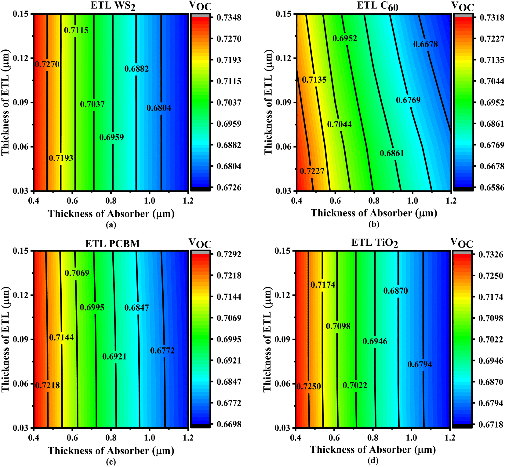 | ||
| Fig. 4 Contour plots of VOC resulting from the sequential change in absorber layer thickness and ETL layer thickness with ETLs including (a) WS2, (b) C60, (c) PCBM, and (d) TiO2. | ||
Fig. 4a illustrates that the maximum VOC levels were observed when the absorber layer thickness was adjusted from 0.4 to 0.45 μm, while the thickness of ETL ranged from 0.03 to 0.15 μm. When the ETL layer thickness increases, the absorber layer thickness remains constant, but VOC may decrease if the absorber layer is increased (Fig. 4a). The thickness of absorber layer remains constant for the C60, PCBM, and TiO2 structures, regardless of the increase in the ETL layer thickness (Fig. 4b–d). No matter how thick the ETL is, the WS2, PCBM, and TiO2 structures attained the greatest value of VOC values considering the thickness of absorber layers are about 0.4 μm and 0.045 μm thick, respectively (Fig. 4a, c and d). Regarding the C60 ETL-based structure, the maximum VOC is found while the thickness of absorber is generally 0.4 to 0.45 μm and the thickness of the ETL is around 0.07 μm (Fig. 4b). Overall, most of the solar systems that were considered might have fewer VOC with increasing absorber layer, as shown in Fig. 4. An increase in saturation current exceeding the photocurrent in the presence of a thick absorber layer can explain this phenomenon by increasing the carrier recombination rate.68
In Fig. 5, we observe how the JSC parameters of four different perovskite solar cells are affected by using different ETL and absorber layer thicknesses. The maximum JSC values (36.77–37.24 mA cm−2) for WS2-based solar cells are noted when the thickness of absorber is between 0.89 and 1.2 μm and the thickness of ETL is between 0.03 and 0.15 μm (Fig. 5a). Based on absorber thicknesses of 0.89–1.2 μm, the PCBM and TiO2 ETL-based solar cells exhibit the same pattern, with peak JSC values of 36.77–37.25 mA cm−2 and 36.77–37.26 mA cm−2, respectively (Fig. 5c and d). Increasing the absorber thickness while maintaining the ETL thickness results in higher JSC values. If the absorber layer is thicker, higher light absorption, providing a higher generation rate and JSC values. To minimize the effects of series resistance, thinner ETL layers may raise the current by decreasing the amount of recombination between electron–hole pairs. Keeping the ETL thickness at a minimum is recommended to enhance JSC, VOC, and overall efficiency. This will help minimize the production of large pinholes and rough surfaces. For WS2, PCBM, and TiO2 ETL-based solar cells, the appropriate absorber thickness is usually determined to be between 0.89 and 1.2 μm, and the ETL thickness does not affect JSC fluctuation (Fig. 5a, c and d). Finally, Fig. 5b shows that the C60-based ETL solar cells have the greater JSC value (35.61–36.85 mA cm−2) when the absorber thickness is between 0.68 and 1.2 μm and the ETL thickness is between 0.03 and 0.05 μm. The observation shows that a smaller ETL and a thicker absorber may result in a higher JSC for C60. Increasing the generation rate and greater JSC is possible with a larger absorber layer since it improves light absorption.68 The impact of series resistance may be alleviated by a thin electron transport layer (ETL), which enhances current by diminishing the chance of recombination of electron–hole pairs. Crucially for JSC, reducing the ETL thickness mitigates the development of bigger pinhole and uneven surface.68
 | ||
| Fig. 5 Contour plots of JSC resulting from the sequential change in absorber layer thickness and ETL layer thickness with ETLs including (a) WS2, (b) C60, (c) PCBM, and (d) TiO2. | ||
Fig. 6 depicts the change of the fill factor (FF) for perovskite solar cells following variations in the absorber and ETL thickness. For Cs2CuBiBr6-based PSCs, the WS2 ETL had an FF of 78.98% when the thickness of absorber layer was between 0.4 and 0.5 μm and the ETL thickness was between 0.03 and 0.15 μm, shown in Fig. 6a. When the thickness of absorber varies from 0.4 to 0.5 μm and the thickness of ETL varies from 0.03 to 0.15 μm, the FF value is observed in solar cells connected to ETLs C60, PCBM, and TiO2-related solar cells, as shown in Fig. 6b–d. This pattern is almost identical to the one that we have found. With the increase in thickness of the absorber layer, the value of FF decreases, and it is not affected by the change in the thickness of the ETL. Alteration to the ETL's thickness may lead to a relationship between rising series resistance and falling FF with increasing absorber thickness.69
 | ||
| Fig. 6 Contour plots of FF resulting from the sequential change in absorber layer thickness and ETL layer thickness with ETLs including (a) WS2, (b) C60, (c) PCBM, and (d) TiO2. | ||
Fig. 7 depicts contour plots that demonstrate changes in PCE for different solar structures when the thickness of the absorber and ETL layers is changed. The ETL WS2 solar design attained optimal efficiency of 19.71% within the absorber thickness range of 0.50 to 0.65 μm and the ETL thickness range of 0.03 to 0.15 μm shown in Fig. 7a. When the absorber thickness varied from 0.5 to 0.65 μm and the ETL thickness varied from 0.03 to 0.15 μm, the devices that employed TiO2 ETL also demonstrated an excellent PCE of 19.65%, illustrated in Fig. 7d. According to Fig. 7c, the PCBM ETL also demonstrated consistent PCEs of 19.55%, with an absorber thickness ranging from 0.55 to 0.65 μm and an ETL thickness ranging from 0.03 to 0.085 μm. In contrast to alternative devices, the PSC with C60 ETL demonstrated the lowest PCE of 19.42%, with an absorber thickness between 0.43 to 0.75 μm and an ETL thickness of around 0.03 μm, as seen in Fig. 7b.
 | ||
| Fig. 7 Contour plots of PCE resulting from the sequential change in absorber layer thickness and ETL layer thickness with ETLs including (a) WS2, (b) C60, (c) PCBM, and (d) TiO2. | ||
3.4. Variation of absorber layer thickness and defect density on PV performance for Cs2CuBiBr6
Since there is a direct relationship between defect density (Nt) and the absorber layer thickness, the entire thickness of the absorber layer has a major impact on the efficient operation of solar cells (SCS) and photovoltaic (PV) devices.68 A decrease in stability and PCE occurs in PSCS as a result of film disintegration with the creation of pinholes caused by an increase within the defect density (Nt) in the absorber layer.70 This section explores the overall effect of defect density (Nt) and absorber thickness on a photovoltaic cell that is based on a Cs2CuBiBr6 absorber. Fig. 8–11 shows the results of the simulations that analyzed the effect of different absorber thicknesses (0.4−1.2 μm) and Nt values (1 × 10¹⁵ − 1 × 1019 cm−3) on the PV performance characteristics of the four optimal PSCs. | ||
| Fig. 8 Contour plots of VOC resulting from the concurrent variation in defect density and absorber layer thickness with ETLs including (a) WS2, (b) C60, (c) PCBM, and (d) TiO2. | ||
Fig. 8 illustrates the impact contour plot visualization on the VOC parameter for properties being examined. This visualization was applied to sequentially change the thickness of the absorber layer and Nt. When absorber thickness varies between 0.4–0.8 μm and Nt varies between 1 × 10¹⁵ − 1 × 1017 cm−3, the highest VOC that can be produced using WS2-based ETLs is 0.7360 V, as shown in Fig. 8a. The VOC for TiO2 ETL-related PSC is 0.7340 V when the absorber thickness is between 0.4–0.8 μm and Nt is between 1 × 10¹⁵ − 1 × 1017 cm−3, depicts in Fig. 8d. A constant VOC of 0.7320 V was also demonstrated by the C60 ETL, with absorber thicknesses ranging from 0.4–0.8 μm and Nt ranging from 1 × 10¹⁵ − 1 × 1017 cm−3, illustrated in Fig. 8b. Compared to other devices, the PSC with PCBM ETL exhibited the lowest VOC of 0.730 V, with an absorber thickness varying between 0.4–0.8 μm and Nt between 1 × 10¹⁵ − 1 × 1017 cm−3, as seen in Fig. 8c. It was noted that when absorber thickness was varied with defect densities for WS2, C60, PCBM, and TiO2, a similar impact was seen with ETL-based SC configurations.
The effect of changing absorber thickness and defect density on JSC is demonstrated in Fig. 9a, c and d. When the absorber thickness is between 0.7–1.2 μm and Nt fluctuates between 1 × 10¹⁵ − 1 × 1017 cm−3, the JSC for WS2, PCBM, and TiO2 ETLs achieves 37.30 mA cm−2. In contrast, at the same thickness of the absorber and Nt ranges, the C60-based optimal device attains a JSC value of 35.70 mA cm−2, illustrated in Fig. 9b. Therefore, as the absorber thickness and defect density increase, the JSC value also increases.
 | ||
| Fig. 9 Contour plots of JSC resulting from the concurrent variation in defect density and absorber layer thickness with ETLs including (a) WS2, (b) C60, (c) PCBM, and (d) TiO2. | ||
Regarding all four structures under consideration, Fig. 10 depicts the impact of varying Nt and absorber layer thickness on FF. When the absorber thickness is between 0.4–0.8 μm and the Nt falls within the range of 1 × 10¹⁵ − 1 × 1017 cm−3, the WS2-based PSC achieves the highest FF of 79.00%, shown in Fig. 10a. The result for TiO2 is also similar, according to Fig. 10d. Conversely, the solar cell design based on ETL, C60 shows smaller FF values, measuring 78.80% in cases when the absorber thickness ranges between 0.4–0.8 μm and the Nt value ranges between 1 × 10¹⁵ − 1 × 1017 cm−3, illustrated in Fig. 10b. Similarly, ETL PCBM exhibits the same result in Fig. 10c within the same range of absorber thickness and defect density (Nt).
 | ||
| Fig. 10 Contour plots of FF resulting from the concurrent variation in defect density and absorber layer thickness with ETLs including (a) WS2, (b) C60, (c) PCBM, and (d) TiO2. | ||
Finally, the efficiency (PCE) is defined with variations in absorber thickness and defect density (Nt), shown in Fig. 11. According to Fig. 11a and d, the absorber thickness ranges from 0.4–0.8 μm and the Nt ranges from 1 × 10¹⁵ − less than 1 × 1017 cm−3, resulting in the maximum efficiency for WS2 and TiO2 being 19.70%. Fig. 11c displays an almost similar PCE of 19.60% for a PCBM-based optimized device when the absorber thickness is between 0.4–0.8 μm and Nt is between 1 × 10¹⁵ − less than 1 × 1017 cm−3. In contrast with the other ETLs in Fig. 11b, the ETL-based solar structure C60 exhibits lower PCE values, recording 18.70% at the same absorber thickness and defect density (Nt) ranges. For every device structure, the optimal thickness of ETLs is a crucial factor in achieving the highest possible PCE value.
 | ||
| Fig. 11 Contour plots of PCE resulting from the concurrent variation in defect density and absorber layer thickness with ETLs including (a) WS2, (b) C60, (c) PCBM, and (d) TiO2. | ||
3.5. Impact of absorber layer and HTL layer thickness of several ETLs on PV performance for Cs2CuBiBr6
 | ||
| Fig. 12 Impact of photovoltaic (PV) variables (PCE, FF, JSC and VOC) given the modification in (a) absorber thickness and (b) HTL thickness of Cs2CuBiBr6. | ||
3.6. Impact of series resistance, shunt resistance and temperature of several ETLs on PV performance for Cs2CuBiBr6
 | ||
| Fig. 13 Impact of photovoltaic (PV) variables (PCE, FF, JSC and VOC) given the modification in (a) series resistance (b) shunt resistance and (c) temperature of Cs2CuBiBr6. | ||
 | (11) |
Previous studies indicate that as the PSC temperature increases, the VOC value decreases due to the presence of more defects.51 The bandgap decreased with increasing temperature, which had little effect on the current. However, this alternation appears to remain stable as the temperature rises, despite its small size. The FF and PCE of the device are affected by changes in diffusion length and Rs, which happen as temperature increases.77,78
3.7. Effect of capacitance, Mott–Schottky, generation and recombination rate of several ETLs on PV performance for Cs2CuBiBr6
 | (12) |
 | ||
| Fig. 14 Distinctions in (a) capacitance (b) Mott–Schottky (c) generation and (d) recombination of Cs2CuBiBr6. | ||
According to Fig. 14b, the variables εr, q, V, and ε0 stand for the donor's dielectric constant, electronic charge, applied voltage, and vacuum permittivity, respectively.79 Vbi is produced by the prolongation of the linear component to the voltage axis, whereas Nd is produced by the gradient of the linear component. In both scenarios (Fig. 14a and b), the voltage varies between −0.8 to 0.8 V, and the frequency remains constant at 1 MHz. All enhanced devices exhibit an exponential rise in capacitance with increasing applied voltage, as shown in Fig. 14a. At 0.6 V, the solar structures based on WS2, C60, PCBM, and TiO2 ETL exhibit an exponential rise. Particularly, the PCBM-based ETL configuration has the greatest capacitance value, at about 710 nF cm−2. The capacitance value of the C60-based PSC is approximately 661 nF cm−2, while the WS2 and TiO2 ETL-based PSCs have capacitance values of approximately 680 nF cm−2 and 693 nF cm−2, respectively. Various ETL-associated solar configurations, as depicted in Fig. 14a, could represent the independent voltage capacitance resulting from the saturation of the depletion layer capacitance. Prior studies have shown that even at low voltages, the current remains substantially below saturation values, and that saturation occurs only at voltage peaks located at the points of contact.80 This material has significant prospects as a voltage-controlled solar cell since its capacitance fluctuates as an effect of voltage.
Conversely, the built-in potential (Vbi), which is the difference between the electrode operation and doping level operations, may be effectively and widely determined with the M–S. The p–n junction is the main structure of the M–S theory, with the x-axis intercept usually referring to the Vbi of the semiconductor devices. Different electrode operation functions are used to find the slope of 1/C2(V), which hows the percentage of engaged entrapment centers with lower values as expected.81
| G(λ,x) = α(λ,x)Nphot(λ,x) | (13) |
In contrast, the generation rate involves the creation of new electrons and holes in the conduction band, whereas the recombination rate involves their elimination. The lifetime and charge carrier density of a solar cell define its recombination rate. In the initial stages, the existence of defect states inside the absorber layer causes a decrease in the amount of electron–hole recombination. Consequently, the formation of energy levels impacts the electron–hole recombination rate inside the solar cell structure. In this case, WS2 ETL-based PSCs have a maximum recombination rate of 0.303 μm, shown in Fig. 14d.
3.8. J–V and QE characteristics of Cs2CuBiBr6
With voltage ranging from 0 to 0.72 V, Fig. 15a depicts the fluctuating pattern of the J–V characteristics for the four solar cell structures in the investigation. The current density of the C60-associated PSC is roughly 34.07 mA cm−2, as shown in Fig. 15a, while the JSC of the PCBM-associated device is almost 35.59 mA cm−2. The other two ETL-associated devices perform better than the C60 and PCBM-associated devices. In Fig. 15a, the ETL-associated structures of WS2 and TiO2 showed an open circuit voltage density of unity and a current density of 35.63 mA cm−2. The device's efficiency is greatly affected by defects in perovskite films because photoelectrons are created inside these layers. The behavior of electron–hole recombination significantly influences the photovoltaic characteristics of the PSC. The interaction between the J–V curve and the bulk trap density is shown in Fig. 15a for a perovskite film. If defect states exist in perovskite films, there is a significant drop in all photovoltaic films. These findings are consistent with the assumption that perovskite solar structures with a high degree of crystallinity reduce charge recombination and improve performance.82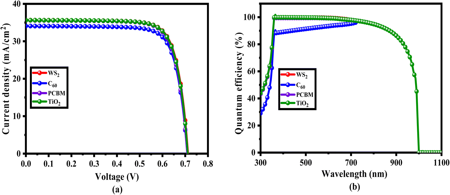 | ||
| Fig. 15 Optimization of the (a) J–V characteristic curve and (b) the quantum energy curve of Cs2CuBiBr6. | ||
Fig. 15b exhibits the quantum efficiency (QE) graphs for all the devices associated with the research. In this case, the wavelength is changed from 300 to 1100 nm. The exponential increase is seen in Fig. 15b for all structures in the 300 to 360 nm range. The value is consistent across a wide range of around 360 to 600 nm. The QE of the PSCs according to the research at that time was determined to be unaffected by wavelength. Subsequently, the quantum efficiency declines across all structures as the wavelength increases. The QE for the ITO/C60/Cs2CuBiBr6/CBTS/Ni PSC in Fig. 15b was slightly lower than that of the other structures. In contrast, regarding wavelength variation, the other three PSCs showed approximately equivalent levels of efficiency. As the thickness of the absorber rises, the quantum efficiency (QE) also rises. This happens because a thicker absorber can absorb more photons.83
3.9. Results from SCAPS-1D are compared to earlier research
The performance characteristics of four device combinations with the recently published optimal configurations are compared in Table 4. Compared to the previously reported Cs2CuBiBr6 device structure, Table 4 demonstrates that the optimal Cs2CuBiBr6 double perovskite-based solar cell exhibits a higher PCE value. Four sets of device structures were presented with power conversion efficiencies (PCEs) of 19.70%, 18.69%, 19.52%, and 19.65%. In contrast, previously published device structures, such as the FTO/WS2/Cs2CuBiBr6/spiro-OMeTAD/Ag configuration, show a considerably reduced efficiency of around 14.08%.21 The exhibited solar structures have greater VOC levels compared to the published configurations of devices. Conversely, the solar structure that has been given exhibits greater JSC and FF values than the previously reported Cs2CuBiBr6-based device structure. All of the solar structures mentioned have VOC values over 0.7 V and FF values above 77%, but the device structure that was previously published has the lowest VOC and FF values. The four solar structures shown in Table 4 performed more effectively than the previously described Cs2CuBiBr6-based solar cells.| Type | Optimized devices | VOC (V) | JSC (mA cm−2) | FF (%) | PCE (%) | Ref. |
|---|---|---|---|---|---|---|
| a E – experimental, T – theoretical. | ||||||
| E | FTO/TiO2/Cs2AgBiBr6/spiro-OMeTAD/MoO3/Ag | 1.01 | 3.82 | 65 | 2.51 | 84 |
| E | FTO/c-TiO2/mTiO2/Cs2AgBiBr6/N719/spiro-OmeTAD/Ag | 1.06 | 5.13 | — | 2.84 | 85 |
| E | FTO/TiO2/Cs2AgBiBr6/spiro-OMeTAD/Au | 1.511 | 3.89 | 51.76 | 3.04 | 86 |
| T | ITO/SnO2/Cs2AgBiBr6/spiro-OMeTAD/Au | 0.92 | 11.4 | 60.93 | 6.37 | 87 |
| T | FTO/WS2/Cs2CuBiBr6/spiro-OMeTAD/Ag | 0.60 | 34.59 | 67.36 | 14.08 | 21 |
| T | FTO/TiO2/Cs2AgSbBr6/spiro-OMeTAD/Ag | 0.94 | 22.49 | 50.2 | 10.69 | 21 |
| T | ITO/WS2/Cs2CuBiBr6/CBTS/Ni | 0.712 | 35.63 | 77.57 | 19.70 | This work |
| T | ITO/C60/Cs2CuBiBr6/CBTS/Ni | 0.709 | 34.07 | 77.39 | 18.69 | This work |
| T | ITO/PCBM/Cs2CuBiBr6/CBTS/Ni | 0.709 | 35.59 | 77.35 | 19.52 | This work |
| T | ITO/TiO2/Cs2CuBiBr6/CBTS/Ni | 0.711 | 35.62 | 77.52 | 19.65 | This work |
The performance parameters of the four device configurations that were presented in Table 4 are compared to the optimum configurations that were recently published. In comparison to the previously reported Cs2B′B′′Br6 device structure, Table 4 demonstrates that the optimal Cs2CuBiBr6 double perovskite-based solar cell exhibits a greater PCE value. In Table 4, the fifth solar cell device structure used spiro-OMeTAD HTL, resulting in 14.08% efficiency compared to our present study of HTL CBTS. The emphasis of our investigation was on the properties of the absorber, such as its defect density, which were different from those of previous theoretical research on device structures. The characteristics of our study's ETL and HTL combinations also differed from those used in previous theoretical assessments. The optical characteristics of the absorber also influence the absorption of solar energy. By achieving 14.08% PCE in the FTO/WS2/Cs2CuBiBr6/spiro-OMeTAD/Ag structure, the improved optical characteristics of the Cs2CuBiBr6 absorber were observed.21 The above justifies the conclusion that, compared with previously researched Cs2CuBiBr6-based, differently structured solar cells, our Cs2CuBiBr6 solar cell exhibits superior PCE.
4. Conclusion
The research objective is to investigate the SCAPS-1D simulation results and determine the possibility of developing perovskites based on cesium copper bismuth bromide. The four solar designs (ITO/WS2/Cs2CuBiBr6/CBTS/Ni, ITO/C60/Cs2CuBiBr6/CBTS/Ni, ITO/PCBM/Cs2CuBiBr6/CBTS/Ni, ITO/TiO2/Cs2CuBiBr6/CBTS/Ni) are compared in terms of their PV properties. Among all the investigated structures, ITO/WS2/Cs2CuBiBr6/CBTS/Ni demonstrated the greatest performance with PCE of 19.70%, VOC of 0.712 V, JSC of 35.63 mA cm−2, and FF of 77.57%. An advantageous band alignment is responsible for this higher performance. The absorber layer falls within the range of 0.4 to 1.2 μm, with the highest efficiency occurring at 0.6 μm. The thickness of the electron transport layers (ETLs) varies between 0.03 and 0.15 μm for the four different perovskite solar cell structures. Device efficiency is further improved by optimizing the HTL thickness between 0.1 and 0.5 μm. PV characteristics are greatly impacted by changes in defect density (Nt), whereas PCE and FF are adversely affected by series resistance without significantly impacting JSC and VOC. While VOC, FF, and PCE increase with shunt resistance, enhancing at 102 Ω cm2, the JSC stays constant. From 300 to 450 K, the performance of WS2-based ETL structures remains preferable; as the temperature rises, PCE, VOC, and FF drop but JSC stays constant. In particular, at around 710 nF cm−2, the PCBM-based ETL structure has the highest capacitance value. When the rates of generation and recombination were investigated, the ITO/WS2/Cs2CuBiBr6/CBTS/Ni structures exhibited the maximum recombination at 0.303 μm and the ITO/TiO2/Cs2CuBiBr6/CBTS/Ni configurations showed the most generation at 0.7 μm. J–V characteristics and quantum efficiency (QE) analysis both demonstrated superior performance WS2 ETL devices. For the development of double perovskite-based innovations, these outcomes provide significant information for improving solar cell designs.Data availability
Data will be made available on request.Author contributions
Khandoker Isfaque Ferdous Utsho: investigation, methodology, data curation, conceptualization, writing original manuscript; S. M. G. Mostafa: investigation, methodology, data curation, review-editing; Md. Tarekuzzaman: formal analysis, software, conceptualization, review-editing; Muneera S. M. Al-Saleem: formal analysis, methodology, data curation, review-editing; Nazmul Islam Nahid: formal analysis, methodology, data curation, review-editing; Jehan Y. Al-Humaidi: formal analysis, methodology, data curation, review-editing; Md. Rasheduzzaman: formal analysis, validation, review-editing; Mohammed M. Rahman: formal analysis, validation, supervision, review-editing; Md. Zahid Hasan: formal analysis, validation, supervision, review-editing.Conflicts of interest
There is no conflict to declare.Acknowledgements
This research is funded by Princess Nourah bint Abdulrahman University Researchers Supporting Project number (PNURSP2025R80), Princess Nourah bint Abdulrahman University, Riyadh, Saudi Arabia.References
- M. Hosenuzzaman, N. A. Rahim, J. Selvaraj, M. Hasanuzzaman, A. A. Malek and A. Nahar, Renewable Sustainable Energy Rev., 2015, 41, 284–297 CrossRef.
- K. Ranabhat, L. Patrikeev, A. A. Revina, K. Andrianov, V. Lapshinsky and E. Sofronova, J. Appl. Eng. Sci., 2016, 31, 103532 Search PubMed.
- S. B. Verma, Emerging Trends in IoT and Computing Technologies, 2022 Search PubMed.
- J. N. Davis, Master's thesis, The University of Utah, 2023.
- A. M. Bagher, M. Vahid and M. Mohsen, Int. J. Renewable Sustainable Energy, 2014, 3, 59–67 CrossRef.
- H. Al Dmour, East Eur. J. Phys., 2023, 3, 555–561 CrossRef.
- H. Al-Dmour, D. M. Taylor and J. A. Cambridge, J. Phys. D:Appl. Phys., 2007, 40, 5034 CrossRef.
- M. T. Kibria, A. Ahammed, S. M. Sony, F. Hossain and S. U. Islam, in Proc. of 5th, 2014, pp. 51–53 Search PubMed.
- K. K. Sharma, D. I. Patel and R. Jain, Chem. Commun., 2015, 51, 15129–15132 RSC.
- H. Al-Dmour and D. M. Taylor, Thin Solid Films, 2011, 519, 8135–8138 CrossRef.
- A. Slami, M. Bouchaour and L. Merad, Int. J. Energy Environ., 2019, 13, 17–21 Search PubMed.
- S. Karthick, S. Velumani and J. Bouclé, Sol. Energy, 2020, 205, 349–357 CrossRef.
- A. Aftab and M. I. Ahmad, Sol. Energy, 2021, 216, 26–47 CrossRef.
- F. Baig, Y. H. Khattak, B. Marí, S. Beg, A. Ahmed and K. Khan, J. Electron. Mater., 2018, 47, 5275–5282 CrossRef.
- H. Al-Dmour, R. H. Alzard, H. Alblooshi, K. Alhosani, S. AlMadhoob and N. Saleh, Front. Chem., 2019, 7, 561 CrossRef CAS PubMed.
- A. K. Mishra and R. K. Shukla, SN Appl. Sci., 2020, 2, 321 CrossRef CAS.
- H. Al-Dmour, S. Al-Trawneh and S. Al-Taweel, Int. J. Adv. Appl. Sci., 2021, 8, 128–135 CrossRef.
- H. Kolya and C.-W. Kang, Polymers, 2023, 15, 3421 CrossRef CAS PubMed.
- S. Shahi, PhD thesis, State University of New York at Buffalo, 2022.
- H. Al-Dmour and D. M. Taylor, J. Ovonic Res., 2023, 19(5), 587–596 CrossRef CAS.
- R. Yao, S. Ji, T. Zhou, C. Quan, W. Liu and X. Li, Phys. Chem. Chem. Phys., 2024, 26, 5253–5261 RSC.
- Z.-L. Huang, C.-M. Chen, Z.-K. Lin and S.-H. Yang, Superlattices Microstruct., 2017, 102, 94–102 CrossRef CAS.
- W. S. Yang, J. H. Noh, N. J. Jeon, Y. C. Kim, S. Ryu, J. Seo and S. I. Seok, Science, 2015, 348, 1234–1237 CrossRef CAS PubMed.
- E. T. McClure, M. R. Ball, W. Windl and P. M. Woodward, Chem. Mater., 2016, 28, 1348–1354 CrossRef CAS.
- G. Volonakis, M. R. Filip, A. A. Haghighirad, N. Sakai, B. Wenger, H. J. Snaith and F. Giustino, J. Phys. Chem. Lett., 2016, 7, 1254–1259 CrossRef CAS PubMed.
- F. Igbari, Z. Wang and L. Liao, Adv. Energy Mater., 2019, 9, 1803150 CrossRef.
- X.-G. Zhao, D. Yang, J.-C. Ren, Y. Sun, Z. Xiao and L. Zhang, Joule, 2018, 2, 1662–1673 CrossRef CAS.
- H. Absike, N. Baaalla, R. Lamouri, H. Labrim and H. Ez-zahraouy, Int. J. Energy Res., 2022, 46, 11053–11064 CrossRef.
- H. Wu, A. Erbing, M. B. Johansson, J. Wang, C. Kamal, M. Odelius and E. M. J. Johansson, ChemSusChem, 2021, 14, 4507–4515 CrossRef PubMed.
- H.-J. Feng, W. Deng, K. Yang, J. Huang and X. C. Zeng, J. Phys. Chem. C, 2017, 121, 4471–4480 CrossRef.
- J. Burschka, N. Pellet, S.-J. Moon, R. Humphry-Baker, P. Gao, M. K. Nazeeruddin and M. Grätzel, Nature, 2013, 499, 316–319 CrossRef PubMed.
- H. Bencherif and M. K. Hossain, Sol. Energy, 2022, 248, 137–148 CrossRef.
- Y.-F. Chiang, J.-Y. Jeng, M.-H. Lee, S.-R. Peng, P. Chen, T.-F. Guo, T.-C. Wen, Y.-J. Hsu and C.-M. Hsu, Phys. Chem. Chem. Phys., 2014, 16, 6033–6040 RSC.
- S. Ryu, J. H. Noh, N. J. Jeon, Y. C. Kim, W. S. Yang, J. Seo and S. I. Seok, Energy Environ. Sci., 2014, 7, 2614–2618 RSC.
- V. Sebastian and J. Kurian, Sol. Energy, 2021, 221, 99–108 CrossRef.
- H. Bencherif, L. Dehimi, N. Mahsar, E. Kouriche and F. Pezzimenti, Mater. Sci. Eng., B, 2022, 276, 115574 CrossRef.
- M. Khaouani, A. Hamdoune, H. Bencherif, Z. Kourdi and L. Dehimi, Optik, 2020, 217, 164797 CrossRef.
- F. Kherrat, L. Dehimi, H. Bencherif, M. M. A. Moon, M. K. Hossain, N. A. Sonmez, T. Ataser, Z. Messai and S. Özçelik, Micro Nanostruct., 2023, 183, 207676 CrossRef.
- S. Chen, Y. Pan, D. Wang and H. Deng, J. Electron. Mater., 2020, 49, 7363–7369 CrossRef.
- Y. Pan and W. Guan, J. Power Sources, 2016, 325, 246–251 CrossRef CAS.
- J. Zhou, J. Hou, X. Tao, X. Meng and S. Yang, J. Mater. Chem. A, 2019, 7, 7710–7716 RSC.
- X. Guo, H. Dong, W. Li, N. Li and L. Wang, ChemPhysChem, 2015, 16, 1727–1732 CrossRef CAS PubMed.
- B. Zaidi, N. Mekhaznia, M. S. Ullah and H. Al-Dmour, J. Phys.: Conf. Ser., 2024, 2843, 012012 CrossRef CAS.
- N. L. Dey, Md. S. Reza, A. Ghosh, H. Al-Dmour, M. Moumita, Md. S. Reza, S. Sultana, A. K. M. Yahia, M. Shahjalal, N. S. Awwad and H. A. Ibrahium, J. Phys. Chem. Solids, 2025, 196, 112386 CrossRef CAS.
- X. Shi, Y. Ding, S. Zhou, B. Zhang, M. Cai, J. Yao, L. Hu, J. Wu, S. Dai and M. K. Nazeeruddin, Adv. Sci., 2019, 6, 1901213 CrossRef CAS.
- L. Cojocaru, S. Uchida, Y. Sanehira, J. Nakazaki, T. Kubo and H. Segawa, Chem. Lett., 2015, 44, 674–676 CrossRef CAS.
- K. Wang, Z. Jin, L. Liang, H. Bian, D. Bai, H. Wang, J. Zhang, Q. Wang and S. Liu, Nat. Commun., 2018, 9, 4544 CrossRef.
- Y. H. Khattak, F. Baig, H. Toura, S. Beg and B. M. Soucase, J. Electron. Mater., 2019, 48, 5723–5733 CrossRef CAS.
- D. Shin, B. Saparov, T. Zhu, W. P. Huhn, V. Blum and D. B. Mitzi, Chem. Mater., 2016, 28, 4771–4780 CrossRef CAS.
- R. Chakraborty, K. M. Sim, M. Shrivastava, K. V. Adarsh, D. S. Chung and A. Nag, ACS Appl. Energy Mater., 2019, 2, 3049–3055 CrossRef CAS.
- M. K. Hossain, M. H. K. Rubel, G. F. I. Toki, I. Alam, Md. F. Rahman and H. Bencherif, ACS Omega, 2022, 7, 43210–43230 CrossRef CAS PubMed.
- M. H. Ali, A. S. Islam, M. D. Haque, M. F. Rahman, M. K. Hossain, N. Sultana and A. T. Islam, Mater. Today Commun., 2023, 34, 105387 CrossRef.
- R. Pandey, S. Bhattarai, K. Sharma, J. Madan, A. K. Al-Mousoi, M. K. A. Mohammed and M. K. Hossain, ACS Appl. Electron. Mater., 2023, 5, 5303–5315 CrossRef CAS.
- A. K Al-Mousoi, M. K. A. Mohammed, S. Q. Salih, R. Pandey, J. Madan, D. Dastan, E. Akman, A. A. Alsewari and Z. M. Yaseen, Energy Fuels, 2022, 36, 14403–14410 CrossRef CAS.
- A. K. Al-Mousoi, M. K. Mohammed, R. Pandey, J. Madan, D. Dastan, G. Ravi and P. Sakthivel, RSC Adv., 2022, 12, 32365–32373 RSC.
- R. A. Jabr, M. Hamad and Y. M. Mohanna, Int. J. Electr. Eng. Educ., 2007, 44, 23–33 CrossRef.
- Y. H. Khattak, PhD thesis, Universitat Politècnica de València, 2019.
- F. Anwar, S. Afrin, S. Satter, R. Mahbub and S. M. Ullah, Int. J. Renew. Energy Res., 2017, 7, 885–893 Search PubMed.
- Y. Gan, X. Bi, Y. Liu, B. Qin, Q. Li, Q. Jiang and P. Mo, Energies, 2020, 13, 5907 CrossRef.
- Y. Raoui, H. Ez-Zahraouy, N. Tahiri, O. El Bounagui, S. Ahmad and S. Kazim, Sol. Energy, 2019, 193, 948–955 CrossRef.
- K. Sekar, L. Marasamy, S. Mayarambakam, H. Hawashin, M. Nour and J. Bouclé, RSC Adv., 2023, 13, 25483–25496 RSC.
- T. Minemoto and M. Murata, Sol. Energy Mater. Sol. Cells, 2015, 133, 8–14 CrossRef.
- H. Abnavi, D. K. Maram and A. Abnavi, Opt. Mater., 2021, 118, 111258 CrossRef.
- D. K. Maram, M. Haghighi, O. Shekoofa, H. Habibiyan and H. Ghafoorifard, Sol. Energy, 2021, 213, 1–12 CrossRef.
- O. Gunawan, T. K. Todorov and D. B. Mitzi, Appl. Phys. Lett., 2010, 97, 233506 CrossRef.
- C. Yan, F. Liu, N. Song, B. K. Ng, J. A. Stride, A. Tadich and X. Hao, Appl. Phys. Lett., 2014, 104, 173901 CrossRef.
- S. Rai, B. K. Pandey and D. K. Dwivedi, Opt. Mater., 2020, 100, 109631 CrossRef.
- M. K. Hossain, A. A. Arnab, R. C. Das, K. M. Hossain, M. H. K. Rubel, M. F. Rahman, H. Bencherif, M. E. Emetere, M. K. Mohammed and R. Pandey, RSC Adv., 2022, 12, 35002–35025 Search PubMed.
- S. Abdelaziz, A. Zekry, A. Shaker and M. Abouelatta, Opt. Mater., 2020, 101, 109738 CrossRef.
- J. A. Owolabi, M. Y. Onimisi, J. A. Ukwenya, A. B. Bature and U. R. Ushiekpan, Am. J. Phys. Appl., 2020, 8, 8–18 Search PubMed.
- U. Mandadapu, S. V. Vedanayakam and K. Thyagarajan, Indian J. Sci. Technol., 2017, 10, 65–72 Search PubMed.
- M. K. Hossain, D. P. Samajdar, R. C. Das, A. A. Arnab, Md. F. Rahman, M. H. K. Rubel, Md. R. Islam, H. Bencherif, R. Pandey, J. Madan and M. K. A. Mohammed, Energy Fuels, 2023, 37, 3957–3979 CrossRef CAS.
- E. Bi, W. Tang, H. Chen, Y. Wang, J. Barbaud, T. Wu, W. Kong, P. Tu, H. Zhu and X. Zeng, Joule, 2019, 3, 2748–2760 Search PubMed.
- E. H. Jung, N. J. Jeon, E. Y. Park, C. S. Moon, T. J. Shin, T.-Y. Yang, J. H. Noh and J. Seo, Nature, 2019, 567, 511–515 CrossRef CAS PubMed.
- D. Bogachuk, R. Tsuji, D. Martineau, S. Narbey, J. P. Herterich, L. Wagner, K. Suginuma, S. Ito and A. Hinsch, Carbon, 2021, 178, 10–18 CrossRef CAS.
- A. Sunny, S. Rahman, M. Khatun and S. R. A. Ahmed, AIP Adv., 2021, 11, 065102 Search PubMed.
- S. R. Raga, E. M. Barea and F. Fabregat-Santiago, J. Phys. Chem. Lett., 2012, 3, 1629–1634 CrossRef CAS PubMed.
- F. Behrouznejad, S. Shahbazi, N. Taghavinia, H.-P. Wu and E. W.-G. Diau, J. Mater. Chem. A, 2016, 4, 13488–13498 RSC.
- S. Lin, Computer Solutions of the Traveling Salesman Problem, Bell Syst. Tech. J., 1965, 44, 2245–2269 CrossRef.
- G. G. Malliaras, J. R. Salem, P. J. Brock and C. Scott, Phys. Rev. B:Condens. Matter Mater. Phys., 1998, 58, R13411–R13414 CrossRef CAS.
- M. Samiul Islam, K. Sobayel, A. Al-Kahtani, M. A. Islam, G. Muhammad, N. Amin, M. Shahiduzzaman and M. Akhtaruzzaman, Nanomaterials, 2021, 11, 1218 CrossRef PubMed.
- M. Liu, M. B. Johnston and H. J. Snaith, Nature, 2013, 501, 395–398 CrossRef CAS.
- K. K. Maurya and V. N. Singh, J. Sci.:Adv. Mater. Devices, 2022, 7, 100445 Search PubMed.
- F. Igbari, R. Wang, Z.-K. Wang, X.-J. Ma, Q. Wang, K.-L. Wang, Y. Zhang, L.-S. Liao and Y. Yang, Nano Lett., 2019, 19, 2066–2073 Search PubMed.
- X. Yang, Y. Chen, P. Liu, H. Xiang, W. Wang, R. Ran, W. Zhou and Z. Shao, Adv. Funct. Mater., 2020, 30, 2001557 CrossRef CAS.
- E. Greul, M. L. Petrus, A. Binek, P. Docampo and T. Bein, J. Mater. Chem. A, 2017, 5, 19972–19981 RSC.
- Z. Zhang, Q. Sun, Y. Lu, F. Lu, X. Mu, S.-H. Wei and M. Sui, Nat. Commun., 2022, 13, 3397 Search PubMed.
| This journal is © The Royal Society of Chemistry 2025 |