DOI:
10.1039/D4RA08323G
(Paper)
RSC Adv., 2025,
15, 7342-7353
Probing high-efficiency Cs0.05(FA0.77MA0.23)0.95Pb(I0.77Br0.23)3-based perovskite solar cells through first principles computations and SCAPS-1D simulation†
Received
24th November 2024
, Accepted 22nd February 2025
First published on 7th March 2025
Abstract
This study presents a high-efficiency perovskite solar cell structure, incorporating a Cs0.05(FA0.77MA0.23)0.95Pb(I0.77Br0.23)3 as absorber, PCBM as the electron transport layer (ETL), and CuSbS2 as the hole transport layer (HTL). First-principles calculations were conducted to explore the electronic and optical properties of these materials, revealing a high absorption coefficient of approximately 105 cm−1, making the perovskite an excellent absorber. The SCAPS-1D simulation tool was employed to evaluate the photovoltaic performance of the ITO/PCBM/mixed perovskite/CuSbS2/Ag device. Various factors such as different HTLs and ETLs, absorber thickness, ETL and HTL thickness, defect concentration, temperature, and resistance were analyzed to optimize device performance. The results demonstrate that the optimized configuration achieves an outstanding power conversion efficiency of 28.01%, with an open-circuit voltage of 1.12 V, a short-circuit current density of 29.84 mA cm−2, and a fill factor of 83.78%. Notably, the study found that HTL thickness variations have a more dominant impact on efficiency than perovskite thickness, emphasizing the importance of transport layer engineering. The findings offer a promising pathway for further research on material optimization, stability enhancement, and large-scale fabrication, paving the way for the next generation of perovskite solar technologies.
1. Introduction
Perovskite solar cells (PSCs) are among the most promising photovoltaic technologies, which in experimental conditions have demonstrated a power conversion efficiency (PCE) of 26.7%.1–4 This remarkable efficiency rivals that of traditional silicon solar cells, establishing PSCs as strong contenders for industrial-scale applications.5,6 The commercialization of PSCs faces significant challenges, particularly their instability under ambient conditions, susceptibility to radiation exposure, and the toxicity of lead (Pb) used in their composition.7 Nevertheless, PSCs offer key advantages, including cost-effectiveness, high performance, enhanced absorption coefficients, and superior charge transport properties, all of which contribute to their high efficiency.8–15 Methylammonium lead iodide (MAPbI3), a widely used absorber layer in PSCs, exhibits exceptional optoelectronic properties.16 However, its stability is compromised by environmental factors such as temperature, moisture, and oxygen, posing a major obstacle to large-scale industrial adoption.7 Compared to thin-film solar cells, the instability caused by moisture and oxygen can be mitigated through encapsulation techniques or by improving interface properties, while thermal stability depends largely on structural components.17
Compositional engineering has emerged as a key strategy for enhancing the performance and stability of perovskite solar cells. Among various perovskite materials, cesium (Cs)-based perovskites exhibit superior thermal stability, making them highly suitable for long-term applications.18 Cs+ incorporation stabilizes the α-phase by optimizing the Goldschmidt tolerance factor, thereby improving structural integrity and phase stability.18 Beyond Cs+ doping, mixed-cation perovskites have gained significant attention due to concerns over lead toxicity and the need for enhanced optoelectronic properties.19 The partial substitution of Cs, methylammonium (MA), and formamidinium (FA) in perovskite compositions such as (Cs/MA/FA)Pb(I/Br)3 offers notable advantages, including improved mechanical robustness, enhanced thermal stability, and intrinsic moisture resistance. These properties, combined with their tunable bandgaps, make mixed-cation perovskites particularly promising for flexible and tandem perovskite solar cells.20 The bandgap engineering plays a crucial role in optimizing energy absorption and charge transport. Advanced mixed-cation, mixed-halide perovskites with carefully tuned bandgaps and optimized p–i–n device architectures have led to significant efficiency gains. Notably, triple-cation compositions (FA, MA, Cs) with bandgaps ranging from 1.59 to 1.68 eV have achieved higher efficiencies as an absorber layer in PSCs, demonstrating their potential for high-performance photovoltaic applications.21–23 Regardless of the bandgap of perovskite material and its energy level alignment with adjacent charge transport layers, selecting optimal electron transport layer (ETL) and hole transport layer (HTL) materials is crucial for designing high-performance single-junction perovskite solar cells. The ETL plays a vital role in PSCs, facilitating efficient charge extraction and transport. Among the most promising ETL materials, tin oxide (SnO2)24 and phenyl-C71-butyric acid methyl ester (PCBM)25,26 offer several advantages, including high electron mobility, a wide bandgap, chemical stability, and excellent optical transmittance. Additionally, their low-temperature processability makes them suitable for flexible and lightweight substrates, expanding the potential for next-generation photovoltaic applications. Similarly, the HTL is essential for optimizing PCE by ensuring efficient hole extraction and reducing recombination losses. Copper thiocyanate (CuSCN)27 and (CuO2)28 have emerged as promising HTL candidates due to their high hole mobility, favorable energy level alignment with perovskite materials, and ability to suppress recombination at the HTL/perovskite interface. Among emerging HTLs, (copper antimony sulfide) (CuSbS2) offers distinct advantages, including well-matched energy levels with the absorber layer, which enhances hole collection and transport while minimizing energy losses. Moreover, its excellent chemical stability and compatibility with perovskite materials contribute to improved device longevity. The high absorption coefficient and superior optical properties of CuSbS2 further boost light absorption, leading to enhanced photoconversion efficiency.29,30 The performance of mixed-cation lead halide perovskite solar cells has been extensively studied through experimental research21,22,31–33 to achieve higher efficiencies. However, to the best of our knowledge, theoretical investigation23 on device performance and performance modeling for mixed perovskite solar cells remain limited.
In this study, we investigate a Cs0.05(FA0.77MA0.23)0.95Pb(I0.77Br0.23)3-based perovskite solar cell, exploring various hole transport layers (HTLs)—V2O5 (vanadium pentoxide), CuO2, CuSCN, CBTS (copper bismuth thiophosphate), and CuSbS2—and electron transport layers (ETLs)—SnO2, ZnO, C60, IGZO (indium gallium zinc oxide), and PCBM. Using SCAPS-1D simulations, we systematically evaluate these ETL-HTL combinations to identify the optimal theoretical pairing within an ITO/ETL/perovskite/HTL/Ag architecture. To further validate the structural and optical properties of the selected perovskite absorber, we perform first-principles calculations based on density functional theory (DFT), confirming its band gap characteristics. Additionally, we analyze the impact of absorber and ETL thicknesses on photovoltaic performance, as well as the effects of series (Rs) and shunt (Rsh) resistance and operating temperature on the best-performing configuration. By unraveling the intricate interplay of these parameters, our study provides valuable insights into efficiency and stability optimization in perovskite solar cells. This comprehensive theoretical investigation not only enhances the fundamental understanding of device physics but also paves the way for future advancements in perovskite-based photovoltaics.
2. Details of calculation
The calculations were performed using the QuantumATK software.34 All geometries were fully optimized using the Perdew–Burke–Ernzerhof functional with generalized gradient approximation (GGA-PBE).35 A medium basis set pseudopotential from the norm-conserving PseudoDojo36 was applied. Brillouin zone sampling utilized a 5 × 5 × 6 Monkhorst–Pack k-point mesh, with a cutoff energy of 105 Ha for primitive cell lattice optimization. Electronic calculations employed a 3 × 3 × 3 and 5 × 7 × 2 k-point grid for mixed perovskite and CuSbS2, respectively. Convergence criteria were set at 0.03 eV Å−1 for force and 10−5 eV for energy throughout the optimization process.
The proposed device architecture for simulating a high-efficiency PSC, as shown in Fig. S1,† comprises of multiple layers with specific thicknesses and material compositions: ITO (0.05 μm), PCBM (0.1 μm), mixed perovskite (0.4 μm), and CuSbS2 (0.1 μm). ITO (indium tin oxide) is a transparent conducting oxide exploited like bottom contact, allowing light to pass through while providing a conductive surface for electron flow. PCBM (phenyl-C61-butyric acid methyl ester), a fullerene derivative commonly used as an electron acceptor in organic solar cells, acts as the efficient ETL by extracting electrons generated by the material that absorbs radiance.37 The mixed perovskite is the key of PSC, the suggested absorber, is a mixed-halide perovskite material composed of Cs, FA, MA, Pb, iodine(I), and bromine (Br). This layer absorbs sunlight and generates electron–hole pairs, initiating the photovoltaic effect. CuSbS2 serves as HTL, promoting the movement of holes, or positive charges, from the mixed perovskite layer to the front contact, making it a promising material for enhancing the cell's overall efficiency.38 Besides, Tables S1 and S2† provide the input parameters of the absorption coefficient values used for each layer as well as the electrical properties of the interfaces. The simulations were carried out under standard conditions, specifically at 300 K ambient temperature and AM 1.5 G lighting. Additionally, we took great care in defining the simulation parameters for the different HTLs, ETLs, and the absorber, as elaborated in Tables S3 and S4.†
The SCAPS-1D39 software effectively solves the equations governing Poisson, continuity, and drift-diffusion. The following eqn (1) is a basic building block for comprehending charge distribution and electrostatics in semiconductor materials. The electric field E can be expressed as the gradient of the electrostatic potential ϕ.40
| |
 | (1) |
where
εr is the relative permittivity,
ε0 represents the permittivity of free space
q is the charge,
p and
n denote the electron and hole concentrations, respectively.
ND+ is the donor density,
NA− is the acceptor density, and
ρp and
ρn represent the charge density of hole and electron, respectively. The following equation describes the device's carrier continuity formulas:
41| |
 | (2) |
| |
 | (3) |
Here,
Jn and
Jp denote for the current densities of electrons and holes, respectively.
G is the generation rate, and
R stands for the recombination rate. Additionally, carrier current density can be acquired from:
42| |
 | (4) |
| |
 | (5) |
The charge is represented by q, the carrier mobilities by μp, μn, and the diffusion coefficients by Dp, Dn.
3. Results and discussion
3.1 First principles results analysis
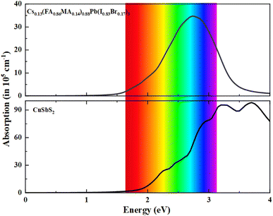
Let us now examine the geometric structure of the supercell containing (Cs/FA/MA)Pb(I/Br)3, CuSbS2 (chalcostibite), and PCBM molecule. To model the mixed lead halide perovskite, we start from cubic phase of FAPbI3 by using a 2 × 2 × 2 supercell, as shown in Fig. S2a.† The structure of CuSbS2 consists of continuous SbS2 units aligned with the b-axis formed by sharing edges between square pyramidal SbS5 units (see Fig. S2b†). The optimized lattice constants for Cs0.14(FA0.85MA0.14)0.88Pb(I0.83Br0.17)3 are found to be a = 11.853 Å, b = 12.270 Å, and c = 12.203 Å. The computed lattice parameters for CuSbS2, with values of a = 6.160 Å, b = 3.843 Å, and c = 14.311 Å, closely match experimental results (a = 6.134 Å, b = 3.911 Å, and c = 14.549 Å).43 For electronic characterization, we conducted band structure and density of states calculations for mixed-cation lead halide perovskite at GGA-PBE, and for CuSbS2 at Heyd–Scuseria–Ernzerhof hybrid with spin–orbit coupling (HSE06+SOC), as shown in Fig. 1. Additionally, the lowest unoccupied molecular orbital (LUMO) and highest occupied molecular orbital (HOMO) were ascertained of PCBM using HSE06 functional (see Fig. 1). Our findings reveal that the mixed lead halide perovskite exhibits characteristics of a direct semiconductor band-gap, with the Γ point serving as the location of the conduction band minimum and valence band maximum. The computed band gap is around 1.67 eV, turn it ideal for photovoltaic applications. Conversely, CuSbS2 demonstrates an indirect band gap of 1.59 eV, in close matching comparing to the experimental value of 1.58,44 indicative of its electron transport layer properties. Moreover, the valence band maximum of bulk CuSbS2 is located at the Z point, while the conduction band minimum lies between the R and U points. Lastly, the HOMO–LUMO gap of the PCBM molecule is determined to be 2.08 eV. From a comprehensive standpoint, considering the analysis of combined lead halide perovskite, it is evident that the states near the higher valence band (VB) predominantly derive from Pb s- and (I and Br) p-states. Conversely, the states near the lower band minimum are mainly comprised of Pb p- and (I and Br) p-states, consistent with existing literature ref. 45. The local-projected density of states (DOS) for CuSbS2 is depicted in Fig. 2 and S3.† The top of the valence band is primarily composed of Cu 3d and S 3p states, while the conduction band is mainly formed by Sb 5p and S 3p states, with minor contributions from Sb 5s, Sb 4d, and S 3s states. Consequently, Cu+ (d10) to Cu2+ (d9) may oxidize as a result of the enhancement of a Cu-based electron during photoexcitation.46 This phenomenon could potentially impact hole transport in CuSbS2, particularly as films from concurrent experimental investigations have demonstrated slight copper deficiency.47 Therefore, we conducted calculations to determine the optical absorption coefficient of mixed-cation lead halide perovskites and CuSbS2 (refer to Fig. 3). As illustrated in Fig. 3, the mixed lead halide perovskite exhibits a wide-ranging absorption spectrum within the visible-light range. Notably, when the wavelength falls between 2 to 3 eV, the optical absorption of the studied perovskite material intensifies, with the absorption coefficient surpassing 30 × 10−5 cm−1. These observations highlight the favorable structural stability and strong optical absorption characteristics of mixed-cation lead halide perovskite within the visible light region, indicating its potential suitability as absorbing layer in PSCs. Regarding CuSbS2, analysis of the absorption coefficient curve reveals an initial small peak within the visible light region, followed by a broader peak in the ultraviolet region at an energy level of 3.90 eV, reaching a maximum value of 91 × 105 cm−1.
 |
| | Fig. 1 Computed band structures of (a) mixed-cation lead halide perovskite and (b) CuSbS2. (c) Illustration of the HOMO and LUMO of PCBM molecule. | |
 |
| | Fig. 2 Partial density of the states of (a) mixed-cation lead halide perovskite and (b) CuSbS2 in the equilibrium geometry. The Fermi level was positioned along the dashed black line. | |
 |
| | Fig. 3 Calculated optical absorption coefficients for mixed-cation lead halide perovskite (top) and CuSbS2 (bottom). | |
3.2 Device simulation results analysis
Before optimizing the proposed solar cell's parameters, it is essential to identify compatible ETL and HTL layers. Simulations were conducted with various ETL and HTL materials, revealing that PCBM and CuSbS2 are the most suitable choices based on the PSC's figure of merit. Fig. 4(a) and (b) present radar plots of key PV parameters, including short-circuit current density (JSC), open-circuit voltage (VOC), fill factor (FF), and power conversion efficiency (PCE), for different ETL and HTL combinations. Compared to other materials like C60, SnO2, ZnO, and IGZO, PCBM stands out due to its exceptional electronic properties, including high electron mobility, favorable energy level alignment, excellent solution processability, and film morphology.48 These advantages make PCBM a preferred ETL in many organic solar cell architectures. Additionally, years of research and optimization have established robust processing protocols and a deep understanding of role of PCBM in solar cells.14,25,26 Similarly, CuSbS2 may surpass other HTL materials such as CBTS, V2O5, Cu2O, and CuSCN due to its high hole mobility, tunable energy levels, chemical stability, and cost-effectiveness.49 These attributes position CuSbS2 as a promising HTL for next-generation solar cells. Ongoing research continues to enhance its properties and device performance, aiming to improve photovoltaic efficiency and long-term stability.49 Moreover, the PCBM and CuSbS2 layers play crucial roles in directing charge carriers toward the respective electrodes. PCBM, a fullerene derivative, exhibits high electron mobility, favorable energy level alignment, and low-temperature processability compared to traditional ETLs like TiO2.26 PCBM, with a conduction band minimum (CBM) of 3.95 eV, enables electron extraction from the perovskite CBM (4.5 eV) while blocking hole recombination. CuSbS2, serving as the HTL, has a valence band maximum (VBM) of 3.0 eV, closely aligning with the perovskite VBM (2.82 eV), ensuring efficient hole transport. Additionally, the stability and high absorption of CuSbS2 enhance device performance and longevity.50
 |
| | Fig. 4 (a) Effect of different ETL layers (b) effect of different HTL layers of the performance of PSC. | |
The impact of the mixed perovskite layer thickness on the J–V characteristics of the proposed PSC structure is depicted in Fig. 5(a). As the thickness increases from 0.2 μm to 1.4 μm, the JSC exhibits a notable rise. This trend can be attributed to enhanced light absorption with increasing absorber thickness, which leads to greater photogenerated charge carriers. However, beyond a certain thickness, recombination losses may counteract this benefit, causing JSC to saturate or slightly decline.28 Fig. 5(b) further analyzes the effect of thickness variation on the photovoltaic parameters, including VOC, JSC, FF, and PCE. The VOC follows a decreasing trend as the absorber thickness increases. This decline is primarily caused by increased charge carrier recombination within thicker layers, which hinders charge extraction efficiency. The FF initially increases from 82.5% to 84.4% with thickness but stabilizes beyond 1.0 μm. This behavior suggests that an optimal thickness range exists where series resistance is minimized, ensuring efficient charge transport. The PCE reaches its peak at an absorber thickness of 0.8 μm, achieving a maximum value of 22.5%. Beyond this point, further increasing the thickness results in a slight decline in efficiency, likely due to diminishing gains in JSC and increased recombination losses.51 These findings highlight the importance of optimizing the absorber layer thickness to balance light absorption, charge transport, and recombination effects. The simulation results indicate that an optimal mixed perovskite layer thickness of 0.8 μm provides the highest efficiency for the proposed PSC device. This optimization is critical for enhancing overall device performance and achieving high-efficiency, stable perovskite solar cells.
 |
| | Fig. 5 (a) J–V characteristics; (b) effect of thickness of absorber layer in VOC, JSC, FF and PCE. (c) J–V characteristics; (d) effect of thickness of CuSbS2 HTL in VOC, JSC, FF and PCE. | |
The effect of CuSbS2 HTL thickness on the photovoltaic performance of the perovskite solar cell is analyzed in Fig. 5(c) and (d). As shown in Fig. 5(c), the J–V characteristics indicate that increasing the HTL thickness from 0.1 μm to 0.5 μm results in a decrease in JSC. This decline is primarily due to increased charge transport resistance within the thicker HTL, which limits the efficient extraction of photogenerated carriers. Fig. 5(d) further illustrates the variations in the key PV parameters as a function of CuSbS2 thickness. The JSC decreases from 22 mA cm−2 to 14 mA cm−2 with increasing HTL thickness, which can be attributed to reduced light absorption and enhanced recombination losses in thicker layers. The VOC remains relatively stable, suggesting that changes in HTL thickness do not significantly alter the energy band positions or the alignment of Fermi levels at the interfaces. However, both FF and PCE exhibit a declining trend as the HTL thickness increases beyond 0.1 μm. The increase in series resistance associated with a thicker HTL contributes to this deterioration in performance. These findings emphasize the necessity of optimizing the CuSbS2 HTL thickness to balance hole extraction efficiency, minimize recombination losses, and maintain low contact resistance.52 The optimal thickness of 0.1 μm ensures efficient charge transport while avoiding excessive resistive losses, thereby maximizing the overall performance of the PSC. Optimizing the ETL thickness in a PSC is crucial for achieving efficient electron extraction, minimizing contact and series resistance, reducing charge recombination, and ensuring proper energy level alignment. If the ETL is too thick, charge carriers experience longer transit times, increasing the likelihood of recombination at defect sites. Additionally, ETL thickness impacts energy level alignment at the absorber interface, where an optimal thickness facilitates efficient charge transfer while minimizing energy losses.53 To identify the optimal ETL thickness, we varied it from 0.1 μm to 0.5 μm in increments of 0.1 μm. As shown in Fig. S4,† a thickness of 0.1 μm delivers the best device performance.
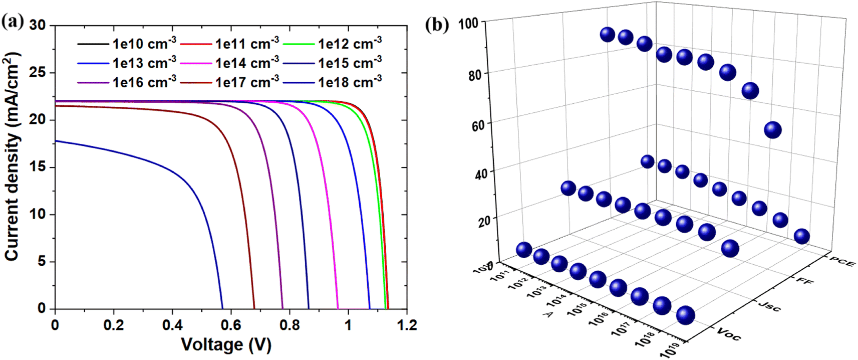
Fig. 6(a) and (b) illustrate the significant impact of defect density on the electrical characteristics and overall performance of PSCs. In Fig. 6(a), the J–V curves shift considerably as the defect density increases from 1010 cm−3 to 1018 cm−3, highlighting the role of trap-assisted recombination. At low defect densities (≤1015 cm−3), the device maintains a high JSC of approximately 24.2 mA cm−2, indicating minimal recombination losses and efficient charge transport. However, as the defect density increases beyond 1016 cm−3, JSC decreases drastically, reaching ∼14 mA cm−2 at 1018 cm−3, due to enhanced recombination and reduced carrier lifetime. Fig. 6(b) further confirms these trends by illustrating the relationship between defect density and key photovoltaic parameters. The results indicate that VOC remains relatively stable at 0.98 V for defect densities up to 1015 cm−3, but decreases to 0.94 V at 1018 cm−3. Similarly, the FF, which remains around 86% for defect densities below 1015 cm−3, drops significantly to ∼70% at 1018 cm−3, reflecting increased charge carrier scattering and higher series resistance. The PCE follows the same trend, starting at ∼20% for defect densities ≤1014 cm−3, but dropping sharply to <10% for densities exceeding 1017 cm−3. This highlights how excessive defect concentrations lead to increased non-radiative recombination, reducing overall device efficiency. To mitigate these negative effects, minimizing defect concentrations in the perovskite absorber layer is crucial. Strategies such as optimizing fabrication processes, improving material purity, introducing defect passivation layers, and developing defect-tolerant perovskite compositions are essential for achieving high-performance and stable PSCs. Understanding and controlling defect-related losses remain key factors in advancing next-generation photovoltaic technologies.
 |
| | Fig. 6 Effect of defect density in (a) J–V characteristics and (b) in VOC, JSC, FF and PCE. | |
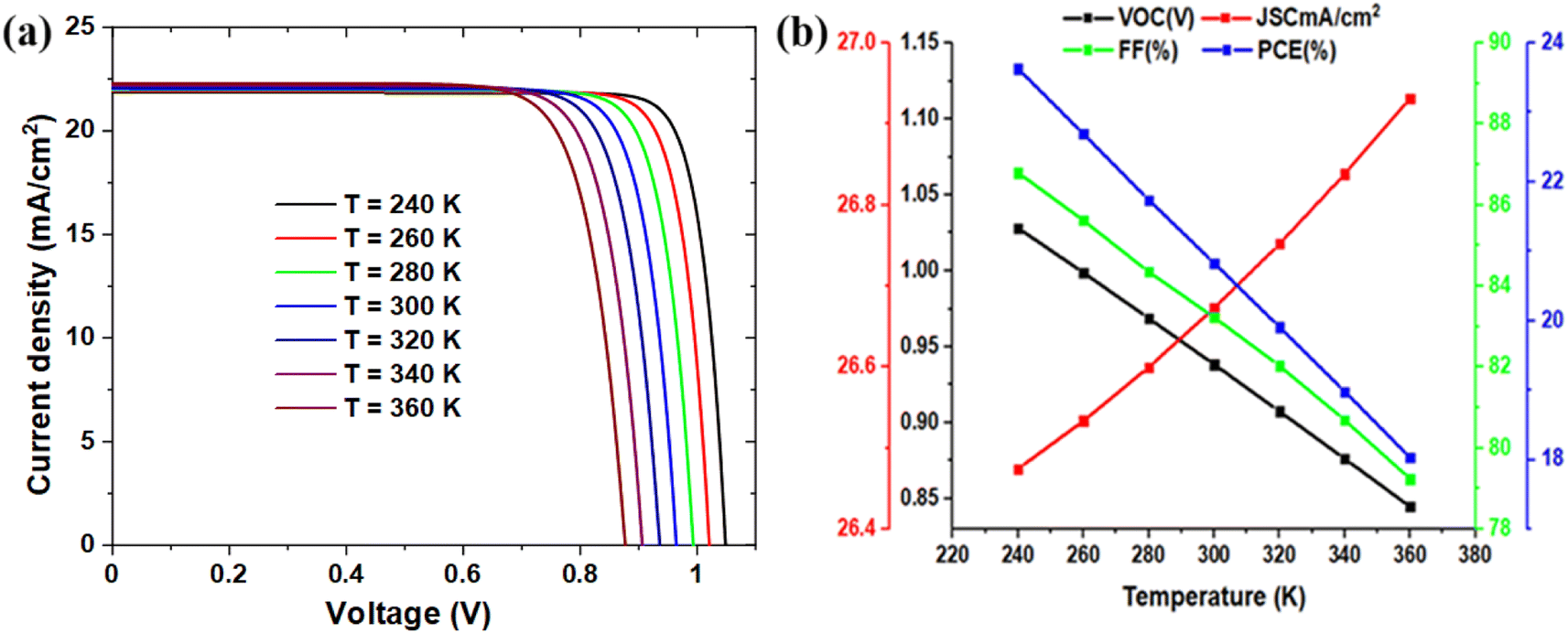
Fig. 7(a) and (b) illustrate the J–V characteristics and impact of temperature variations on the performance of PSCs, with a focus on key photovoltaic parameters. The results confirm that increasing temperature from 240 K to 360 K negatively affects overall device performance, primarily due to enhanced non-radiative recombination and changes in resistive losses. As observed in Fig. 7(b), the VOC exhibits a consistent decline with increasing temperature. This effect arises due to higher carrier recombination rates at elevated temperatures, which reduce the quasi-Fermi level splitting. VOC drops from approximately 1.052 V at 240 K to 0.85 V at 360 K, indicating a thermal-driven energy loss mechanism. Consequently, the PCE follows the same trend, decreasing from around ∼23.8% at 240 K to 18% at 360 K, confirming the strong correlation between temperature and recombination losses. In contrast to VOC, the JSC remains relatively stable across the temperature range. The stability of JSC in PSCs indicates that temperature-induced losses are mainly due to increased recombination rather than changes in charge generation.52 The FF is significantly impacted by temperature, decreasing from ∼87% at 240 K to ∼79% at 360 K. This decline is attributed to increased Rs and reduced Rsh at higher temperatures, leading to efficiency losses. The increase in Rs impedes charge transport, while lower Rsh facilitates leakage currents, further degrading FF and the overall performance. These results highlight the necessity of thermal stability optimization in PSCs.
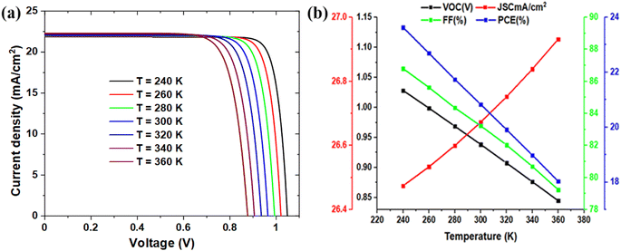 |
| | Fig. 7 Temperature impact from 240 to 360 K in (a) J–V characteristics; (b) VOC, JSC, FF and PCE. | |
Fig. 8(a) and (b) illustrate the variations in photovoltaic parameters of PSCs with changing series resistance (Rs) and shunt resistance (Rsh). The optimization of these resistances plays a critical role in maximizing PSC performance and stability. As observed in Fig. 8(a), increasing Rs from 2 Ω cm2 to 10 Ω cm2 results in a significant decline in FF and PCE. When Rs = 2 Ω cm2, the device achieves a high FF of approximately 80% and PCE close to 18%. However, at Rs = 10 Ω cm2, both FF and PCE drop significantly, with FF reducing to ∼40% and PCE falling below 10%. This confirms that excessive Rs induces voltage losses, increasing power dissipation and reducing device efficiency. Notably, JSC remains relatively stable across the range of Rs, staying between 20–24 mA cm−2, indicating that series resistance primarily affects voltage-dependent parameters rather than current generation. Fig. 8(b) shows the impact of varying Rsh from 104 Ω cm2 to 108 Ω cm2. Higher Rsh values lead to improved device performance by suppressing leakage currents. At Rsh = 108 Ω cm2, the device exhibits a VOC close to 1.05 V, FF around 85%, and a PCE exceeding 20%. In contrast, when Rsh = 104 Ω cm2, the FF drops to 50%, and the PCE falls below 12%, indicating significant recombination losses due to shunt pathways. Notably, JSC remains relatively unaffected, hovering between 22–24 mA cm−2, reinforcing the notion that Rsh mainly influences voltage-related losses rather than photocurrent generation. Achieving high-performance PSCs requires minimizing series resistance (Rs < 2 Ω cm2) and optimizing shunt resistance (RSh > 107 Ω cm2). The findings imply that resistive losses mostly impact voltage-dependent parameters like VOC, FF, and PCE because JSC is rather stable despite changes in Rs and Rsh. While a high Rsh decreases recombination losses, improving VOC and overall efficiency, a high Rs increases series resistance losses, decreasing FF and PCE.54 The maximum PCE (∼20%) is obtained under the optimum conditions (Rs = 2 Ω cm2, Rsh ≈ 108 Ω cm2), indicating that careful resistance engineering is essential for PSC performance. In order to create robust and effective perovskite-based photovoltaics, these results highlight the necessity of improving Rs and Rsh through material selection, fabrication methods, and device engineering.
 |
| | Fig. 8 Variation in PV parameters related to (a) Rs and (b) Rsh. | |
For the final optimization of the simulated device, a mixed perovskite layer with a thickness of 0.8 μm and a defect density of 1017 cm−3 was selected. Fig. 9 and 10 illustrate the influence of ETL and HTL thickness on the performance of the FTO/PCBM/mixed perovskite/CuSbS2 device. The results indicate that a 1.8 μm-thick mixed perovskite layer effectively captures AM 1.5 insolation, minimizing reliance on light reflected from the back electrode. This suggests that the proposed design optimizes light absorption and charge transport without requiring additional optical enhancements. Fig. 10 demonstrates the influence of ETL (0.1–0.5 μm) and absorber thickness (0.2–1.4 μm) on the photovoltaic performance of PSCs, revealing complex trade-offs between light absorption, charge transport, and recombination. The VOC reaches a peak of 0.96 V at an absorber thickness of 0.2 μm with an ETL of 0.1–0.3 μm, but declines with increasing absorber thickness due to enhanced reverse saturation current. The JSC improves with absorber thickness up to an optimal range, beyond which bulk recombination limits further gains. The FF remains high when both layers are optimized, as excessive thickness introduces series resistance and charge recombination losses. Consequently, the highest PCE is observed for absorber thicknesses of 0.6–1.0 μm and ETL thicknesses of 0.1–0.3 μm, balancing light absorption and charge extraction. The results from Fig. 9 emphasize the importance of carefully tuning the ETL and absorber thickness to achieve an optimal balance between light absorption, charge generation, and transport. While a thicker absorber increases JSC, it can also lead to higher recombination losses, negatively affecting VOC and FF. Similarly, an optimal ETL thickness is required to facilitate efficient electron extraction without introducing excessive series resistance. These findings highlight the necessity of jointly optimizing these layers to minimize recombination and resistance losses, thereby maximizing device efficiency and stability.
 |
| | Fig. 9 Effect of absorber versus ETL thickness in (a) JSC, (b) VOC, (c) FF, (d) PCE. | |
 |
| | Fig. 10 Effect of absorber thickness vs. HTL thickness in (a) JSC, (b) VOC, (c) FF, (d) PCE. | |
The 3D plots illustrate the effects of changing the HTL and mixed perovskite thicknesses on solar cell performance (Fig. 10). The mixed perovskite layer thickness varies between 0.2 and 1.4 μm, while the HTL thickness ranges from 0.1 to 0.5 μm. The JSC increases notably with mixed perovskite thickness, reaching approximately 30 mA cm−2 at 1.4 μm, demonstrating enhanced light absorption. However, the VOC declines from 0.97 V to ∼0.89 V beyond 1.0 μm, indicating higher recombination losses. The FF initially increases but stabilizes at ∼84.4% when the mixed perovskite thickness exceeds 1.0 μm, showing that further increases have minimal impact. The PCE peaks at ∼22.5% with an optimal 0.8 μm mixed perovskite and 0.1 μm HTL thickness, achieving a balance between light absorption, charge transport, and recombination losses.55 These trends suggest that while a thicker mixed perovskite layer enhances absorption, excessive thickness leads to VOC degradation and charge transport limitations. The dominance of HTL thickness variations over mixed perovskite in optimizing PCE underscores the importance of finely tuning both layers to minimize series resistance and recombination while maximizing carrier extraction efficiency.
Table 1 compares our results with existing theoretical and experimental studies on mixed perovskite-based PSCs. Our optimized configuration achieved a maximum PCE of 28.01%, significantly outperforming previous experimental and simulation studies,23 which reported efficiencies of around 20%. To refine device performance, we conducted a comprehensive simulation to identify the most efficient ETL, HTL, and their key properties. The primary objective of these simulations was to determine the optimal material combinations that yield the highest efficiency. Notably, our studied configurations demonstrated superior performance compared to previous simulations, offering valuable insights for future device optimization. This substantial improvement underscores the superiority and potential of optimized solar cell designs, paving the way for further advancements and innovations in photovoltaic technology.
Table 1 Comparison of photovoltaic performance characteristics for mixed perovskite-based solar cells
| Structures |
JSC (mA cm−2) |
VOC (V) |
FF (%) |
PCE (%) |
| Initial Configuration |
25.67 |
0.938 |
82.23 |
20.83 |
| Experiment23 |
20.70 |
1.220 |
82.0 |
20.8 |
| Simulation23 |
20.35 |
1.290 |
78.38 |
20.57 |
| Optimized configuration |
29.84 |
1.120 |
83.78 |
28.01 |
4. Conclusion
This study introduces a high-efficiency device structure based on perovskite solar cell, incorporating Cs0.05(FA0.77MA0.23)0.95Pb(I0.77Br0.23)3 as the absorber, PCBM as the ETL, and CuSbS2 as the HTL. DFT calculations were employed to extract the structural and optoelectronic properties of these materials, which were then integrated into SCAPS-1D simulations. The optimized ITO/PCBM/mixed perovskite/CuSbS2/Ag structure demonstrated outstanding photovoltaic performance, achieving an VOC of 1.12 V, a JSC of 29.84 mA cm−2, a FF of 83.78%, and a PCE of 28.01%. These results mark a significant advancement over previous experimental and theoretical studies, where efficiencies were typically limited to ∼20%. A comprehensive analysis was conducted to evaluate the impact of key parameters, including HTL and ETL selection, absorber and transport layer thicknesses, defect concentration, operating temperature, and resistance effects. The findings indicate that a 1.2 μm-thick perovskite absorber and a 0.3 μm HTL provide the optimal balance between light absorption, charge transport, and recombination losses. Furthermore, the study confirms that HTL thickness variations have a more dominant influence on PCE than perovskite thickness, highlighting the importance of precise material engineering in optimizing device efficiency. This substantial improvement in photovoltaic performance underscores the superiority of the optimized structure design and its potential to push the boundaries of high-efficiency perovskite solar cells. This work lays a strong foundation for next-generation solar cell research, providing valuable insights for further material optimization, stability enhancement, and large-scale fabrication.
Data availability
All data were communicated in the paper.
Conflicts of interest
There are no conflicts to declare.
Acknowledgements
Research work of authors, from University Mohamed El Bachir El Ibrahimi, was supported by the DGRSDT of Algeria's Ministry of Higher Education. S. Goumri-Said thank the office of research at Alfaisal University in Saudi Arabia for funding this research work through internal project number 24407. M. B. K. would like to thank Prince Sultan University for their support.
References
- T. Nie, Z. Fang, X. Ren, Y. Duan and S. Liu, Recent advances in wide-bandgap organic–inorganic halide perovskite solar cells and tandem application, Nano-Micro Lett., 2023, 15, 70 CrossRef CAS PubMed.
- Y. Wang, J. Wan, J. Ding, J. Hu and D. Wang, A rutile TiO2 electron transport layer for the enhancement of charge collection for efficient perovskite solar cells, Angew. Chem., Int. Ed., 2019, 58, 9414–9418 CrossRef CAS PubMed.
- J. Park, J. Kim, H.-S. Yun, M. J. Paik, E. Noh, H. J. Mun, M. G. Kim, T. J. Shin and S. I. Seok, Controlled growth of perovskite layers with volatile alkylammonium chlorides, Nature, 2023, 616, 724–730 CrossRef CAS PubMed.
- NREL, Best Research-Cell Efficiency Chart, https://www.nrel.gov/pv/cell-efficiency.html, accessed October 2024.
- L. Chu, S. Zhai, W. Ahmad, J. Zhang, Y. Zang, W. Yan and Y. Li, High-performance large-area perovskite photovoltaic modules, Nano Res. Energy, 2022, 1, 9120024 CrossRef.
- N. Ali, N. Shehzad, S. Uddin, R. Ahmed, M. Jabeen, A. Kalam, A. G. Al-Sehemi, H. Alrobei, M. B. Kanoun, A. Khesro and S. Goumri-Said, A review on perovskite materials with solar cell prospective, Int. J. Energy Res., 2021, 45, 19729–19745 CrossRef CAS.
- Y. Ma and Q. Zhao, A strategic review on processing routes towards scalable fabrication of perovskite solar cells, J. Energy Chem., 2022, 64, 538–560 CrossRef CAS.
- W.-J. Yin, T. Shi and Y. Yan, Unique properties of halide perovskites as possible origins of the superior solar cell performance, Adv. Mater., 2014, 26, 4653–4658 CrossRef CAS PubMed.
- S. Choudhary, Potential functionality of perovskite solar cells: A brief review, J. Condens. Matter, 2023, 1, 4–9 CrossRef.
- G. Li, Z. Su, L. Canil, D. Hughes, M. H. Aldamasy, J. Dagar, S. Trofimov, L. Wang, W. Zuo, J. J. Jeronimo-Rendon, M. M. Byranvand, C. Wang, R. Zhu, Z. Zhang, F. Yang, G. Nasti, B. Naydenov, W. C. Tsoi, Z. Li, X. Gao, Z. Wang, Y. Jia, E. Unger, M. Saliba, M. Li and A. Abate, Highly efficient p-i-n perovskite solar cells that endure temperature variations, Science, 2023, 379, 399–403 CrossRef CAS PubMed.
- Y. Rong, Y. Hu, S. Ravishankar, H. Liu, X. Hou, Y. Sheng, A. Mei, Q. Wang, D. Li, M. Xu, J. Bisquert and H. Han, Tunable hysteresis effect for perovskite solar cells, Energy Environ. Sci., 2017, 10, 2383–2391 RSC.
- Q. Jiang, J. Tong, Y. Xian, R. A. Kerner, S. P. Dunfield, C. Xiao, R. A. Scheidt, D. Kuciauskas, X. Wang, M. P. Hautzinger, R. Tirawat, M. C. Beard, D. P. Fenning, J. J. Berry, B. W. Larson, E. L. Warren, M. C. Beard, J. J. Berry, Y. Yan and K. Zhu, Science, 2022, 378, 295–1300 Search PubMed.
- Y. Yan and K. Zhu, Surface reaction for efficient and stable inverted perovskite solar cells, Nature, 2022, 611, 278–283 CrossRef PubMed.
- E. A. Nyiekaa, T. A. Aika, P. E. Orukpe, C. E. Akhabue and E. Danladi, Development on inverted perovskite solar cells: A review, Heliyon, 2024, 10, e24689 CrossRef CAS PubMed.
- A. Miyata, et al., Direct measurement of the exciton binding energy and effective masses for charge carriers in organic–inorganic tri-halide perovskites, Nat. Phys., 2015, 11, 582–587 Search PubMed.
- D. B. Khadka, et al., Advancing efficiency and stability of lead, tin, and lead/tin perovskite solar cells: strategies and perspectives, Sol. RRL, 2023, 7, 2300535 Search PubMed.
- M. B. Faheem, B. Khan, J. Z. Hashmi, A. Baniya, W. S. Subhani, R. S. Bobba, A. Yildiz and Q. Qiao, Insights from scalable fabrication to operational stability and industrial opportunities for perovskite solar cells and modules, Cell Rep. Phys. Sci., 2022, 3, 100827 Search PubMed.
- M. M. Byranvand, T. Kodalle, W. Zuo, T. Magorian Friedlmeier, M. Abdelsamie, K. Hong, W. Zia, S. Perween, O. Clemens, C. M. Sutter-Fella and M. Saliba, One-step thermal gradient- and antisolvent-free crystallization of all-inorganic perovskites for highly efficient and thermally stable solar cells, Adv. Sci., 2022, 2202441 Search PubMed.
- W.-Q. Wu, et al., Bilateral alkylamine for suppressing charge recombination and improving stability in blade-coated perovskite solar cells, Sci. Adv., 2019, 5, eaav8925 Search PubMed.
- M. Wang, J. Liu, C. Ma, Y. Wang, J. Li and J. Bian, Modular perovskite solar cells with Cs0.05(FA0.85MA0.15)0.95Pb(I0.85Br0.15)3 light-harvesting layer and graphene electrode, J. Electron. Mater., 2022, 51, 2381–2389 CrossRef CAS.
- F. Hou, X. Ren, H. Guo, X. Ning, Y. Wang, T. Li, C. Zhu, Y. Zhao and X. Zhang, Monolithic perovskite/silicon tandem solar cells: A review of the present status and solutions toward commercial application, Nano Energy, 2024, 124, 109476 CrossRef CAS.
- P. S. C. Schulze, A. J. Bett, M. Bivour, P. Caprioglio, F. M. Gerspacher, Ö. S. Kabaklı, A. Richter, M. Stolterfoht, Q. Zhang, D. Neher, M. Hermle, H. Hillebrecht, S. W. Glunz and J. C. Goldschmidt, 25.1% high-efficiency monolithic perovskite silicon tandem solar cell with a high bandgap perovskite absorber, Sol. RRL, 2020, 4, 2000152 CrossRef CAS.
- A. Mohandes, M. Moradi and M. Kanani, Numerical analysis of high-performance perovskite solar cells with stacked ETLs/C60 using SCAPS-1D device simulator, Opt. Quantum Electron., 2023, 55, 533 CrossRef CAS.
- S. Huang, P. Li, J. Wang, J. C.-C. Huang, Q. Xue and N. Fu, Modification of SnO2 electron transport layer: Brilliant strategies to make perovskite solar cells stronger, Chem. Eng. J., 2022, 439, 135687 CrossRef CAS.
- H. Liu, S. Hussain, D. Vikraman, J. Lee, S. H. A. Jaffery, J. Jung, H.-S. Kim and J. Kang, Fabrication of InGaZnO-SnO2/PCBM hybrid electron transfer layer for high-performance perovskite solar cell and X-ray detector, J. Alloys Compd., 2022, 906, 164399 CrossRef CAS.
- L. Kavan, Conduction band engineering in semiconducting oxides (TiO2, SnO2): Applications in perovskite photovoltaics and beyond, Catal. Today, 2019, 328, 50–56 CrossRef CAS.
- S. S. Mali, J. V. Patil, H. Kim, R. Luque and C. K. Hong, Highly efficient thermally stable perovskite solar cells via Cs:NiO/CuSCN double-inorganic hole extraction layer interface engineering, Mater. Today, 2019, 26, 8–18 CrossRef CAS.
- A.-A. Kanoun, M. B. Kanoun, A. E. Merad and S. Goumri-Said, Toward development of high-performance perovskite solar cells based on CH3NH3GeI3 using computational approach, Sol. Energy, 2019, 182, 237–244 CrossRef CAS.
- J. Chen and N.-G. Park, Inorganic hole transporting materials for stable and high-efficiency perovskite solar cells, J. Phys.
Chem. C, 2018, 122, 14039–14063 CrossRef CAS.
- R. Zouache, I. Bouchama, O. Saidani, M. A. Ghebouli, M. S. Akhtar, M. A. Saeed and M. Messaoudi, et al., CGS/CIGS single and triple-junction thin-film solar cell: Optimization of CGS/CIGS solar cell at current matching point, Micro Nanostruct., 2024, 207812 CrossRef CAS.
- S. Wang, A. Wang and F. Hao, Toward stable lead halide perovskite solar cells: A knob on the A/X sites components, iScience, 2022, 25, 103599 CrossRef CAS PubMed.
- C. Liu, X. Zhou, S. Chen, X. Zhao, S. Dai and B. Xu, Hydrophobic Cu2O quantum dots enabled by surfactant modification as top hole-transport materials for efficient perovskite solar cells, Adv. Sci., 2019, 6, 1801169 CrossRef PubMed.
- V. Kumar, D. Kumar, R. D. Chavan, K. P. Kumar, B. Yadagiri, M. Ans, J. Kruszynska, A. Mahapatra, J. Nawrocki, K. Nikiforow, N. Mrkyvkova, P. Siffalovic, P. Yadav, S. Akin, S. P. Singh and D. Prochowicz, Molecular modification of spiro[fluorene-9,9'-xanthene]-based dopant-free hole transporting materials for perovskite solar cells, J. Mater. Chem. A, 2024, 12, 8370 RSC.
- S. Smidstrup, T. Markussen, P. Vancraeyveld, J. Wellendorff, J. Schneider, T. Gunst, B. Verstichel, D. Stradi, P. A. Khomyakov, U. G. Vej-Hansen, M. E. Lee, S. T. Chill, F. Rasmussen, G. Penazzi, F. Corsetti, A. Ojanperä, K. Jensen, M. L. N. Palsgaard, U. Martinez, A. Blom, M. Brandbyge and K. Stokbro, QuantumATK: An integrated platform of electronic and atomic-scale modelling tools, J. Phys.: Condens. Matter, 2020, 32, 015901 CrossRef CAS PubMed.
- J. P. Perdew, K. Burke and M. Ernzerhof, Generalized gradient approximation made simple, Phys. Rev. Lett., 1996, 77, 3865–3868 CrossRef CAS PubMed.
- M. J. van Setten, M. Giantomassi, E. Bousquet, M. J. Verstraete, D. R. Hamann, X. Gonze and G. M. Rignanese, The PSEUDODOJO: Training and grading an 85-element optimized norm-conserving pseudopotential table, Comput. Phys. Commun., 2018, 226, 39–54 CrossRef CAS.
- S. Wang, M. Sina, P. Parikh, T. Uekert, B. Shahbazian, A. Devaraj and Y. S. Meng, Role of 4-tert-butylpyridine as a hole transport layer morphological controller in perovskite solar cells, Nano Lett., 2016, 16, 5594–5600 CrossRef CAS PubMed.
- C. Liu, et al., Highly stable and efficient perovskite solar cells with 22.0% efficiency based on inorganic-organic dopant-free double hole transporting layers, Adv. Funct. Mater., 2020, 30, 1908462 CrossRef CAS.
- M. Burgelman, P. Nollet and S. Degrave, Modeling polycrystalline semiconductor solar cells, Thin Solid Films, 2000, 361, 527–532 CrossRef.
- L. Rakocevic, R. Gehlhaar, T. Merckx, P. Qiu, H. Fledderus and J. Poortmans, Interconnection optimization for highly efficient perovskite modules, IEEE J. Photovolt., 2017, 7(2), 404–408 Search PubMed.
- M. Stuckelberger, T. Nietzold, G. N. Hall, B. West, J. Werner, B. Niesen, C. Ballif, V. Rose, D. P. Fenning and M. I. Bertoni, Charge collection in hybrid perovskite solar cells: relation to the nanoscale elemental distribution, IEEE J. Photovolt., 2017, 7(2), 590–597 Search PubMed.
- M. S. Ali, S. Das, Y. F. Abed and M. A. Basith, Lead-free CsSnCl3 perovskite nanocrystals: Rapid synthesis, experimental characterization and DFT simulations, Phys. Chem. Chem. Phys., 2021, 23, 22184–22198 RSC.
- A. Kyono and M. Kimata, Crystal structures of chalcostibite (CuSbS2) and emplectite (CuBiS2): Structural relationship of stereochemical activity between chalcostibite and emplectite, Am. Mineral., 2005, 90(1), 162–165 CrossRef CAS.
- Y. Rodriguez-Lazcano, M. Nair and P. Nair, CuSbS2 thin film formed through annealing chemically deposited Sb2S3–CuS thin films, J. Cryst. Growth, 2001, 223, 399–406 CrossRef CAS.
- M. S. de Holanda, R. F. Moral, P. E. Marchezi, F. C. Marques and A. F. Nogueira, Layered metal halide perovskite solar cells: A review from structure-properties perspective towards maximization of their performance and stability, EcoMat, 2021, 3(4), e12124 CrossRef CAS.
- J. T. Dufton, A. Walsh, P. M. Panchmatia, L. M. Peter, D. Colombara and M. S. Islam, Structural and electronic properties of CuSbS2 and CuBiS2: Potential absorber materials for thin-film solar cells, Phys. Chem. Chem. Phys., 2012, 14(20), 7229–7233 RSC.
- D. Colombara, L. M. Peter, K. D. Rogers, J. D. Painter and S. Roncallo, Formation of CuSbS2 and CuSbSe2 thin films via chalcogenization of Sb–Cu metal precursors, Thin Solid Films, 2011, 519(21), 7438–7443 CrossRef CAS.
- R. Pandey, et al., Halide composition engineered non-toxic perovskite-silicon tandem solar cell with 30.7% conversion efficiency, Appl. Electron. Mater., 2023, 5(10), 5303–5315 CrossRef CAS.
- B. Yang, et al., CuSbS2 as a promising earth-abundant photovoltaic absorber material: A combined theoretical and experimental study, Chem. Mater., 2014, 26(10), 3135–3143 CrossRef CAS.
- R. Mohammadpour, Potential application of CuSbS2 as the hole transport material in perovskite solar cell: A simulation study, Superlattices Microstruct., 2018, 118, 116–122 CrossRef.
- W. Qarony, Y. A. Jui, G. M. Das, T. Mohsin, M. I. Hossain and S. N. Islam, Optical analysis in CH3NH3PbI3 and CH3NH3PbI2Cl-based thin-film perovskite solar cells, Am. J. Energy Res., 2015, 3(2), 19–24 CAS.
- M. Ferdous Rahman, M. Chowdhury, L. Marasamy, M. K. A. Mohammed, M. D. Haque, S. R. Al Ahmed, A. Irfan, A. R. Chaudhry and S. Goumri-Said, Improving the efficiency of a CIGS solar cell to above 31% with Sb2S3 as a new BSF: a numerical simulation approach by SCAPS-1D, RSC Adv., 2024, 14, 1924–1938 RSC.
- M. B. Kanoun, et al., PInorganic Zn2SnO4 electron transport layer in single-junction perovskite solar cells achieving highly efficient performance exceeding 32.85 %, Sol. Energy, 2025, 284(1), 1–10 Search PubMed.
- A. Yousfi, O. Saidani, Z. Messai, R. Zouache, M. Meddah and Y. Belgoumri, Design and simulation of a triple absorber layer perovskite solar cell for high conversion efficiency, East Eur. J. Phys., 2023,(4), 137–146 CrossRef.
- A. Mohandes and M. Moradi, Improved performance of inorganic CsPbI3 perovskite solar cells with WO3/C60 UTL bilayer as an ETL structure: A computational study, Phys. Scr., 2024, 99(5), 055951 CrossRef CAS.
|
| This journal is © The Royal Society of Chemistry 2025 |
Click here to see how this site uses Cookies. View our privacy policy here. 
 Open Access Article
 This Open Access Article is licensed under a Creative Commons Attribution-Non Commercial 3.0 Unported Licence
 *b,
Abderrahim Yousfia,
Girija Shankar Sahooc and
Mohammed Benali Kanoun
*b,
Abderrahim Yousfia,
Girija Shankar Sahooc and
Mohammed Benali Kanoun