
 Open Access Article
 This Open Access Article is licensed under a Creative Commons Attribution-Non Commercial 3.0 Unported Licence
Quantum dot-based non-volatile memory: a comprehensive outlook
Abu Tahera,
M. Atikur Rahman *ab,
Rana Miaa,
Nasir Uddinb,
Mustavi Islamc,
M. N. I. Khand,
M. Khurshed Alame and
Mohammad A. Alim*a
*ab,
Rana Miaa,
Nasir Uddinb,
Mustavi Islamc,
M. N. I. Khand,
M. Khurshed Alame and
Mohammad A. Alim*a
aDepartment of Electrical and Electronic Engineering, University of Chittagong, Chittagong-4331, Bangladesh. E-mail: atikursomon1@gmail.com; mohammadabdulalim@cu.ac.bd
bDepartment of Electrical and Computer Engineering, University of Missouri Kansas City, Missouri, USA
cDepartment of Computer Science, University of Missouri Kansas City, Missouri, USA
dMaterial Science Division, Bangladesh Atomic Energy Commission, Dhaka-1000, Bangladesh
eDepartment of Physics, Bangladesh University of Engineering and Technology, Dhaka-1000, Bangladesh
First published on 6th May 2025
Abstract
With the rise of digital technology, the use of memory devices is swiftly expanding, and this trend is expected to continue in the forthcoming years. Accordingly, researchers are exploring materials that surpass the performance of those used in traditional memory devices, and notably, there is a considerable interest in quantum dots (QDs). This is primarily due to the fact that quantum dots possess exceptional optical and electric properties. As a result, they have become appealing materials to enhance the performance of non-volatile memory devices. In this review, we outlined the various approaches employed for the synthesis of quantum dots as well as different types of quantum dots used for prototyping different non-volatile memory technologies and their current perspective. Additionally, we compared various key parameters, such as the ON/OFF ratio, retention time, memory window, charge trapping capacity, and multiple voltage levels, of these QD-based memories together with future outlook.
1. Introduction
With digitization expanding across various domains, from personal gadgets to automated industries, the demand for memory devices is increasing rapidly.1–7 A crucial component of the majority of contemporary electronic devices is non-volatile memory (NVM) devices. Computer memory that keeps recorded information even when the power is turned off belongs to NVM systems. NVM is utilized for long-term data storage in a variety of applications, such as firmware, embedded systems, and mass storage devices, such as USB flash drives and solid-state drives (SSDs), in contrast to volatile memory, such as random access memory (RAM), which needs constant power to preserve data. Non-volatile memory technologies have undergone substantial advancements over time. Initially, the foundation of NVM was floating gate MOS transistors, which facilitated the development of NAND flash memory. NAND flash is extensively used owing to its increased density and economical cost. Nevertheless, when technology progressed beyond the 20 nm node, conventional NAND flash faced significant constraints, including scaling challenges, high power consumption, and restricted durability.8 Alternatively, various emerging NVM technologies, including all-optical switching, magnetic tunnel junction (MTJ), resistive random access memory (ReRAM), phase change memory (PCM), spin–orbit torque magnetic random-access memory (SOT-MRAM), and spin-transfer torque magnetic random-access memory (STT-MRAM), offer retention periods exceeding 10 years while improving the memory endurance capability. Endurance of approximately 105 cycles has been reported for CdSe QD-based resistive memory.9 The latency for read and write operations in these memories falls within the range of 1 to 7 ns, demonstrating a significant improvement over flash memory and other charge-based memory, such as dynamic random access memory (DRAM) and electrically erasable programmable read-only memory (EEPROM).10In the last few years, there has been significant interest in quantum dots (QDs) in the fields of electrical engineering, materials science, and physics.11 Quantum dots (QDs) are inorganic semiconductor nanoparticles characterized by a radius smaller than that of Bohr excitons.12–14 The nanoscale size (typically 2–10 nm) and quantum confinement of these nanocrystals result in unique optical and electrical properties. These are crystalline materials whose nanoscale dimensions can be considered negligible. Owing to the confinement of excitons in all three spatial directions, these nanocrystals have quantum mechanical characteristics.15–17
The pursuit of devices characterized by high speed, scalability, and reliability has led to extensive investigations into memory devices based on QDs in recent times. The scientific community is experimenting with various quantum dots such as perovskite quantum dots (PQDs), self-assembled quantum dots (SAQDs), magnetic quantum dots (MQDs), core–shell quantum dots (CSQDs), metal oxide quantum dots (MOQDs), metal alloy quantum dots (MAQDs), graphene oxide quantum dots (GOQDs), graphene quantum dots (GQDs), and silicon quantum dots (SiQDs) for application in non-volatile memory.18–32
Quantum dots possess an adjustable bandgap, allowing precise control of their electrical and optical characteristics via size adjustment. This tunability facilitates the tailoring of quantum dots for particular memory applications, hence improving their performance and efficiency.33 The characteristics of quantum dots, including charge storage capacity and energy levels, are significantly influenced by their dimensions. This size dependence facilitates the construction of memory devices with customized attributes, such as multi-level storage, which may substantially enhance the data storage density.34 Quantum dot materials possess many exceptional qualities, including scalability,33 compatibility with semiconductor production,33,34 enhanced charge retention, and stability.34 Besides, QD-based memories have superior retention times, enhanced ON/OFF ratios, increased charge trapping capacity, multiple storage voltages, low power consumption, and tunable bandgaps, making them very attractive candidates for non-volatile memory applications. These attributes also make quantum dots promising materials for data storage. Fig. 1 illustrates various types of quantum dots and their applications in non-volatile memory device prototyping. Different types of QDs can bring unique advantages towards NVM systems. For examples, self-assembled quantum dots have improved chemical stability and charge retention capacity, enabling longevity and fast read/write operation of NVM.11 Core–shell quantum dots show improved quantum yield (QY) and faster carrier transfer, reducing the excitation recombination losses. Also, they can be integrated with other semiconductors during the fabrication process. These crucial properties make CSQDs another promising agent for NVM.35 Graphene oxide quantum dots also exhibit fast read/write operation for (ReRAM) applications.20,36,37 Graphene-based quantum dots have high electrical conductivity, extensive surface area, minimal operating voltage, rapid switching speed, and enhanced quantum confinement, making them promising materials for non-volatile memory systems.29–31
 | ||
| Fig. 1 Various quantum dots used in non-volatile memory. | ||
The major goal of this review is to determine how various types of quantum dots may be used to improve the performance of non-volatile memory systems. We summarize their synthesis processes, working mechanisms, switching properties, ON/OFF ratios, multiple levels and overall potential as transformational materials in the realm of data storage. By analyzing the benefits and drawbacks of each form of quantum dots, we aim to give insights into the future orientations of non-volatile memory technology and the role of quantum dots in its evolution.
2. Prospects and challenges of QDs in NVM technology
Quantum dots show excellent charge transfer capacity due to their unique electronic structure and ultra-low energy consumption. This enables more efficient data storage and retrieval in NVM cells.15,38 In addition, the optical tuning capabilities of QDs are opening new horizons for the creation of photonic memories, where it is possible to control memory devices using light. Quantum dots (QDs) offer several advantages for non-volatile memory (NVM) devices over conventional material across various aspects.2.1 Scalability
Quantum dots (QDs) significantly enhance the scalability of non-volatile memory (NVM) devices. The electronic properties of QDs are size-dependent, allowing precise control of their behavior by adjusting their size. This is crucial for scaling down memory devices, given that smaller QDs can be used to create more densely packed memory cells. In conventional floating-gate (FG) MOSFETs, the floating gate is a continuous layer that stores charge. As the device scales down, the gate dielectric thickness must also decrease, leading to reliability issues such as charge leakage and dielectric breakdown. Alternatively, QDs act as discrete charge storage nodes. This discrete nature reduces the risk of charge leakage and improves the reliability of the memory device. The tunnel oxide in FG MOSFETs becomes less resistant to defect formation as it scales down, which can cause data loss. In QD-based NVMs, the tunnel oxide can be thicker, while still allowing efficient charge trapping and de-trapping due to the quantum confinement effect. This improves the reliability and endurance of the memory device.2.2 Power consumption
The quantum confinement effect in QDs enables them to operate at lower voltages compared to bulk materials. This is because the energy levels in QDs are quantized, allowing more precise control of their charge states, which allows efficient charge trapping and de-trapping. This efficiency reduces the energy required to write and erase data. In conventional floating-gate (FG) MOSFETs, the continuous floating gate requires higher voltages to move charges in and out, leading to higher power consumption. As a result, QD-based NVMs can achieve the same functionality as conventional devices but with significantly lower power requirements.39 Another concern related to power consumption is the leakage current. In conventional NVM devices, leakage currents can significantly contribute to the power consumption, especially as the device scales down. As mentioned, discrete and isolated charge storage nodes also reduce the likelihood of charge leakage. This isolation helps maintain the stored charge without a continuous power supply, thereby reducing the static power consumption.2.3 Endurance/retention
Endurance refers to the ability of a memory device to withstand numerous program/erase cycles without degradation. QD-based NVMs exhibit improved endurance due to several factors. As an example, the aforementioned fact of reduced charge leakage minimizes the wear and tear on the tunnel oxide layer, which is a common issue in conventional floating-gate transistor memory. The tunnel oxide in QD-based NVMs can be thicker compared to the conventional NVMs, which improves its resistance to defect formation. This reduces the likelihood of charge loss and enhances the endurance of the memory device. The thicker tunnel oxide in QD-based NVMs not only improves the endurance but also enhances the retention by reducing the likelihood of charge leakage through defects. Retention refers to the ability of a memory device to retain stored data over time. QD-based NVMs exhibit enhanced retention due to their quantized energy levels, which makes it more difficult for the trapped charge to escape. In some QD-based NVMs, QDs are clad with materials such as germanium oxide (GeOx). This cladding provides electrical and physical isolation, preventing lateral dot-to-dot conduction and reducing charge leakage.33 Also, controlling the solvent or ligand can control the interatomic distance, which will be discussed in the next section. These facts favor QD high-speed operation in memory devices. For example, GeOx-cladded Ge QDs have shown a negligible shift in threshold voltage over a period of one year (Table 1).40| Aspect | Quantum dots (QDs) | Conventional bulk materials |
|---|---|---|
| Scalability | -Better scaling | -Limited by gate dielectric thickness and reliability issues |
| Power consumption | -Lower operating voltages due to efficient charge trapping and de-trapping | -Higher power consumption due to continuous floating gate |
| -Reduced leakage currents due to discrete charge storage nodes | -Significant leakage currents, especially at smaller scales | |
| Endurance | -Improved endurance with discrete and isolated charge storage nodes | -Higher risk of charge leakage and degradation over time |
| -Reduced defect formation in thicker tunnel oxide | -Tunnel oxide more prone to defects and charge loss | |
| Retention | -Enhanced retention | -Lower retention for higher charge leakage |
| -GeOx cladding provides electrical and physical isolation | -Continuous floating gate more susceptible to charge loss |
2.4 Optimizing the performance of ligand-assisted QDs
The use of insulating ligands during the synthesis of quantum dots (QDs) can significantly impact the performance of non-volatile memory (NVM) devices. These ligands, often long-chain organic molecules such as oleic acid, stabilize the QDs but also hinder charge transport between them. This can reduce the efficiency of NVM devices by limiting the movement of charge carriers, which is crucial for device operation. Thus, to address this issue, researchers often employ ligand exchange techniques to replace these long, insulating ligands with shorter, more conductive ligands. This improves the electronic coupling between QDs, enhancing the charge transport and overall device performance. In this case, sometimes the choice of solvent affects ligand-assisted QDs. Fig. 2(a) shows that employing an appropriate solvent, the interatomic distance can be controlled for the better functionalization of QDs. | ||
| Fig. 2 (a) Effect of solvent on atomic distance. (b) Capping layer effect of 3-MPA and β-Ala on transport properties. Reproduced from ref. 41 with permission from RSC. Copyright 2013, RSC. | ||
When QDs are capped with long, insulating ligands, the distance between the QDs is relatively large, and the electronic wavefunctions of the QDs do not overlap significantly. This results in weak electronic coupling and poor charge transport. Thus, by replacing long, insulating ligands with shorter, more conductive ligands, the distance between QDs can be reduced, allowing their electronic wavefunctions to overlap more. This stronger overlap enhances the electronic coupling, facilitating more efficient charge transfer between QDs. This is because the overlapping electronic wavefunctions create pathways for charge carriers to hop or tunnel from one QD to another in non-volatile memory networks. Hines et al.41 explained the effects of various ligands on the surface of QDs and their influence on the electron wavefunction, as shown in Fig. 2(b). TOPO is a common ligand employed for the synthesis of CdSe QDs, which stabilizes the QDs and protects their surface. In the presence of this ligand, the wavefunctions of electrons and holes are confined to the core of the QDs. The TOPO ligand does not create trap states on the surface of the QDs, and thus the wavefunctions of electrons and holes are generally confined to the core of the QDs. 3-Mercaptopropionic acid (3-MPA) is a thiol-based ligand that creates trap states on the surface of QDs. In the presence of this ligand, the electron wave function is extended towards the surface of QDs, as the thiol group creates electron trap states on the surface of QDs. These trap states prevent electron–hole pair separation and slow down the electron transfer process. β-Alanine (β-Ala) is an amino acid ligand that fills the trap states on the surface of QDs. The amino group of this ligand fills the electron trap states on the surface of QDs and confines the electron wavefunction towards the core of the QDs. In the presence of the β-Ala ligand, the electron–hole pair separation improves and the electron transfer rate increases. Conjugated ligands can also induce changes in the tunneling mechanism of QDs. Fig. 3(a and b) show the analysis of the photoresponsive I–V characteristics of polythiophene conjugated CdSe QD (QD-P3000) and carbazole conjugated QD-CB nanoparticles (NPs) based on the Fowler–Nordheim (F–N) tunneling and direct tunneling models, respectively.
 | ||
| Fig. 3 Fowler–Nordheim (F–N) and direct tunneling models under dark and light conditions with (a) forward conditions of QD-P300 and (b) reverse bias of QD-CB NPs. Energy diagram is shown in the inset. Reproduced from ref. 42 with permission from Springer-Nature. | ||
Fig. 3(a) shows the I–V characteristics of QD-P3000 NPs. At a high forward bias, F–N tunneling behavior is observed, indicating photo-induced charge transport. At a low bias voltage, direct tunneling occurs, where the charge flows across the triangular barrier. Fig. 3(b) shows the I–V characteristics of QD-CB NPs, where F–N tunneling occurs at a high bias and direct tunneling occurs at a low bias. However, compared to QD-P3000 NPs, the photo-induced charge transfer in QD-CB NPs is much weaker because of the insulating molecular block in the CB molecule. This image was used to analyze the photoresponsive charge transport, which showed that QD-P3000 exhibits more efficient charge transfer and photo-responsiveness, whereas QD-CB NP shows a poor charge transport performance. QD-P3000 has a direct n–p junction, which allows efficient energy and charge transfer. The QD-CB has an n-ins-p junction, where an insulating molecular block limits the charge transfer. In this case, ligand-assisted QDs can be optimized through engineering for efficient transport operation in memory devices.
3. Synthesis perspective of quantum dots
3.1 Bottom-up approach
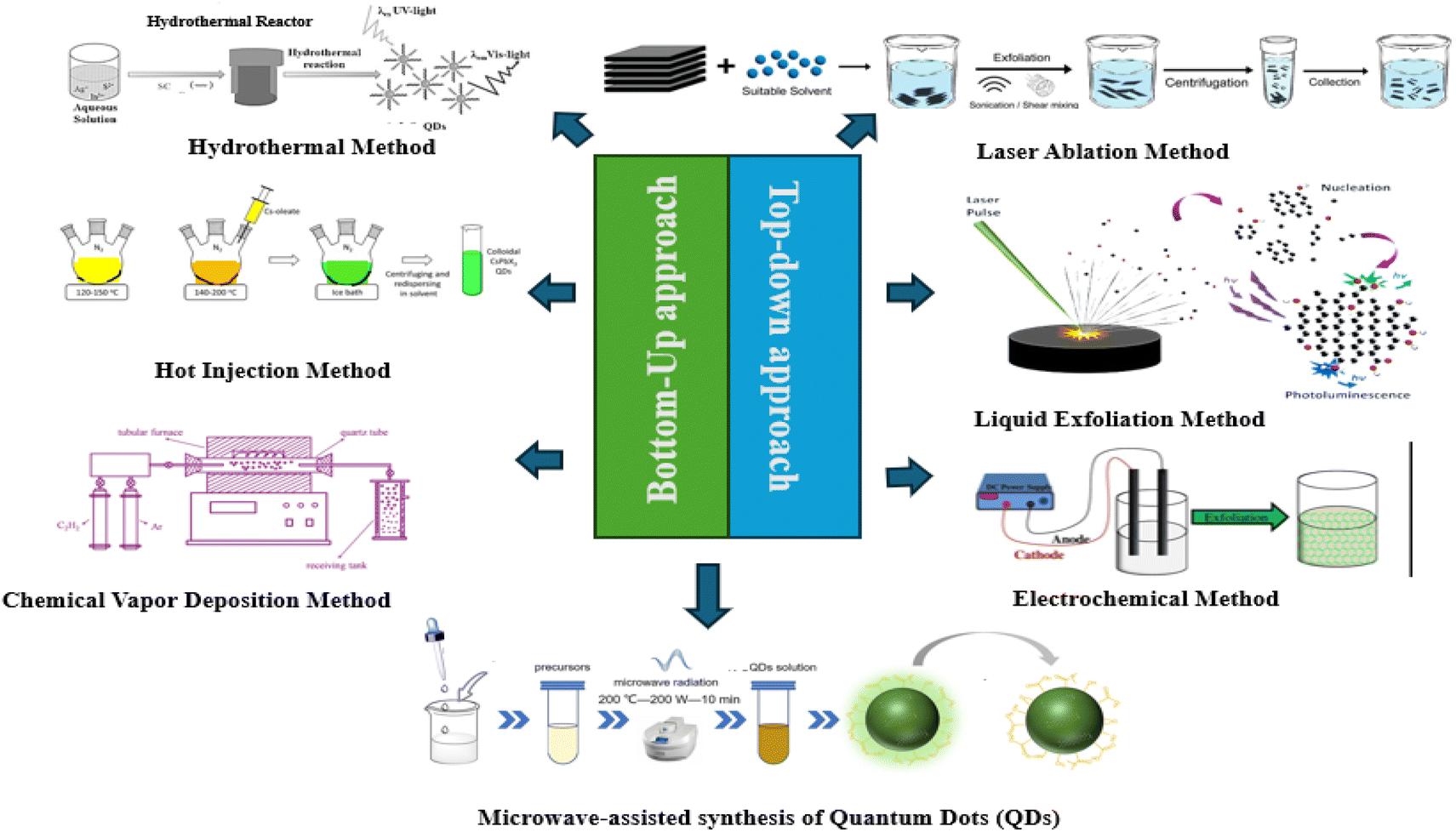 | ||
| Fig. 4 Different synthesis approaches for quantum dots. | ||
Solvothermal synthesis is elegant because of its adaptability. Researchers can produce QDs with precise sizes, forms (ranging from spheres to rods), and even compositions by varying the types and quantities of components, reaction temperature, and reaction time. The light absorption and emission characteristics of these QDs can be further optimized by doping them with additional components. There are various benefits to this approach. It works with a range of QD materials, is easily scaled up for larger volumes, and permits exact control of the features of QDs. Additionally, QDs with great uniformity in size and characteristics are frequently produced by solvothermal synthesis. However, to withstand the tremendous pressure and temperature involved, specific equipment is also needed. Furthermore, some solvents and precursors may be dangerous, necessitating cautious handling and appropriate waste disposal. Notwithstanding these drawbacks, solvothermal synthesis is still a vital method for producing functioning, high-quality quantum dots.55–57 Scientists may unleash the enormous potential of these adaptable nanomaterials by carefully selecting the formulation and reaction conditions, opening the door to breakthroughs in solar cells, LEDs, bioimaging, and many other areas.50,58
One of the major advantages of microwave-assisted synthesis is its versatility. It can be applied to a wide range of precursor materials and solvents, both aqueous and organic. This flexibility allows the synthesis of various types of QDs, such as CdSe, ZnS, and other semiconductor nanocrystals. Additionally, this method is compatible with environmentally friendly solvents and lower reaction temperatures, making it a greener alternative to some conventional synthesis techniques. The rapid heating and cooling cycles enabled by microwave irradiation also facilitate the synthesis of QDs with complex core–shell structures, which are essential for applications requiring specific optical properties.77–80 However, despite its many advantages, microwave-assisted synthesis has some limitations. The scalability of this method can be challenging, given that the uniformity of microwave heating may decrease with larger reaction volumes. Also, specialized microwave reactors are required to ensure consistent and reproducible results, which can be costly and require careful calibration. Moreover, the penetration depth of microwaves can be limited by the dielectric properties of the reaction medium, potentially affecting the synthesis of certain types of QDs. Nevertheless, ongoing advancements in microwave reactor design and process optimization continue to expand the potential of this technique, making it a promising approach for the efficient and sustainable production of high-quality QDs.81–83
3.2 Top-down approach
The capacity of laser ablation to generate high-purity quantum dots is one of its main benefits. The quick quenching of the vaporized material minimizes contamination and enables the creation of nanoparticles with well-defined characteristics. This technique is extremely flexible and may be applied to a variety of materials, such as metals, carbon-based compounds such as graphene and carbon quantum dots, semiconductors such as Ge and Si, and others.84–88 Because of their nanoscale size, the quantum dots created by laser ablation have special optical and electrical properties, making them useful for a variety of applications, including solar cells, photodetectors, and light-emitting diodes (LEDs) in optoelectronics.44,89,90 Also, their intense and stable fluorescence makes them perfect for marking and tracking biological molecules in the field of bioimaging. Additionally, because of their excellent sensitivity and selectivity, quantum dots are used in sensors to identify chemical and biological substances.86,91,92 Laser ablation is a strong and adaptable technique for creating quantum dots, providing exact control of their size and characteristics, excellent purity, and suitability for a variety of materials and uses.87
There are various steps in the electrochemical synthesis process. Firstly, the electrolyte solution dissolves the precursor components. Metal or semiconductor nanoparticles are formed at the cathode when the voltage is applied because the precursor ions are reduced there. Depending on the specific circumstances and materials utilized, these nanoparticles may experience additional oxidation or other surface alterations. When graphite electrodes are utilized in the production of carbon-based quantum dots, such as graphene quantum dots, this approach works especially well. The electrolyte in these cases usually consists of a mixture of bases and acids.94,95 The resulting quantum dots, with their nanoscale dimensions and quantum confinement effects, display distinctive optical and electrical features. Their characteristics make them appropriate for an extensive array of applications, including bioimaging, medication administration, sensing, and optoelectronic devices. Also, because it typically requires gentler temperatures and generates less byproducts than conventional chemical synthesis methods, the electrochemical method is regarded as a green synthesis route.96 Overall, the electrochemical method for the synthesis of quantum dots is a useful technique in nanotechnology and materials research given that it provides a flexible and sustainable way to produce high-quality nanoparticles with customized features.95,97
The bulk material is initially dispersed in an appropriate solvent in liquid-phase exfoliation. The stability of the resultant quantum dots and the effectiveness of exfoliation are both impacted by the choice of solvent, which is critical. Water, ethanol, and organic solvents such as dimethylformamide (DMF) and N-methyl-2-pyrrolidone (NMP) are examples of the common solvents. After the material is distributed, thin nanosheets and quantum dots are created using high shear pressures or ultrasonic waves to break the van der Waals forces keeping their layers together. Numerous variables, including the length and force of sonication, the material concentration in the solvent, and the solvent type, can be changed to regulate the size and quality of the generated quantum dots. For example, smaller and more homogeneous quantum dots can be achieved with increased power and longer sonication durations.
In order to maintain a stable dispersion of quantum dots, surfactants or stabilizers in the solvent can also aid in preventing the re-aggregation of the exfoliated layers.100–102 Because liquid-phase exfoliation is easy to use, scalable, and economical, it is very beneficial. It is suitable for large-scale production because it doesn't require high temperatures or sophisticated equipment. Additionally, this process is eco-friendly, particularly when water or other green solvents are used. Excellent optical and electrical properties render the quantum dots generated via liquid-phase exfoliation useful for a multitude of applications, such as bioimaging, sensors, and optoelectronics. In general, liquid-phase exfoliation is a scalable, ecologically benign, and very effective technique for producing high-quality quantum dots. It provides exact control over the size and characteristics of the dots.103,104 Table 2 illustrates the different quantum dot synthesis techniques, highlighting their respective benefits and drawbacks.
| Method | Type | Advantages | Disadvantages | Examples | Ref. |
|---|---|---|---|---|---|
| Hot injection | Bottom-up | High-quality, monodisperse QDs, precise size control | Requires high temperature, complex setup | CdSe, PbS | 105 and 106 |
| Solvothermal | Bottom-up | Simple setup, scalable, high crystallinity | Long reaction time, high pressure | ZnS, CdTe | 107–109 |
| Hydrothermal | Bottom-up | Environmentally friendly, low cost | Limited to water-soluble precursors | CdS, ZnO | 110–112 |
| Microwave-assisted | Bottom-up | Rapid synthesis, uniform heating, energy-efficient | Limited scalability, specialized equipment | CdSe, ZnS | 113 and 114 |
| Laser ablation | Top-down | No chemical precursors needed, high purity | Expensive equipment, low yield | Si, Ge | 88 and 115 |
| Liquid-phase exfoliation | Top-down | Simple, scalable, no need for high temperature | Produces QDs with wide size distribution | Graphene QDs | 116 and 117 |
| Electrochemical | Top-down | Precise control over size and composition | Requires conductive substrates, complex setup | CdSe, ZnO | 118 and 119 |
| Soft-template | Bottom-up | High surface area, tunable pore size | Template removal can be challenging | ZnS, SiO2, TiO2, C, graphene | 90, 120 and 121 |
| Pyrolysis | Bottom-up | High yield, continuous production possible | High temperature required, potential for toxic by-products | CdSe, InP | 122 and 123 |
| Chemical vapor deposition | Bottom-up | High purity, good control over thickness and composition | Requires high temperature, expensive equipment | Si, Ge | 124–126 |
4. Different quantum dots in non-volatile memory systems
4.1 Perovskite quantum dots (PQDs)
Perovskites are a common class of materials with the general formula ABX3. In this configuration, ‘A’ and ‘B’ represent two cations with markedly different sizes, while ‘X’ denotes an anion that establishes bonds with both cations.38 These nano-sized crystals are a product of perovskite materials, initially defined as metal oxides possessing an octahedral crystal structure similar to that of natural calcium titanate (CaTiO3). Perovskite quantum dots (PQDs) merge the distinctive semiconductor properties of bulk perovskite structures with the precise exciton dynamics made possible by the quantum confinement effect.127,128 This suggests that the semiconductor traits of PQDs can be adjusted through quantum size and surface engineering.17,129,130 Perovskites have been utilized in non-volatile memory devices because of their exceptional electronic properties and the flexibility offered by dimensionality engineering.16,131 There is a considerable relationship between the dimensions of perovskite materials and the operational efficiency of these memory devices.16,18,132 | ||
| Fig. 5 Schematic of CF formation and annihilation in CsPbI3 PQD-based device across various states: (a) iLRS; (b) HRS; (c) IRS; and (d) fLRS. Reproduced from ref. 133 with permission from ACS. Copyright 2024, ACS. | ||
4.1.1.1 Write operation. The ‘write’ operation in PQD-based NVMs is usually accomplished by transferring an external electric field, which causes halide vacancies (such as iodine and bromine vacancies) to migrate within the PQD lattice. As a result of this migration, conductive filaments (CFs) grow between the electrodes of the device, turning it from a high-resistance (HRS) to a low-resistance (LRS) state and decreasing its resistance. The ‘SET’ operation describes this procedure.133
4.1.1.2 Read operation. The ‘read’ function in these devices entails supplying a reduced voltage that is inadequate to modify the existing conductive pathways. The resistance state (HRS or LRS) of the device can be ascertained by measuring the resultant current, which corresponds to the stored data bits (‘0’ or ‘1’).133
4.1.2.1 Resistance switching memory. Resistance switching memory, often referred to as resistive memory or memristor, represents innovative non-volatile memory technology. It operates by altering the electrical resistance of a material between a low resistance state (LRS) and a high resistance state (HRS) when an adequate electric voltage is applied. This mechanism functions similarly to a switch that relies on varying resistance levels, enabling data storage without requiring continuous power to preserve the information.134 A conductive filament is formed within the material when a voltage pulse is applied, resulting in a substantial decrease in resistance (LRS). The filament can be broken by reversing the voltage polarity, which will restore the resistance to a high state (HRS).135 Z. Chen et al.18 synthesized CsPbBr3, an inorganic perovskite quantum dot, and experimentally proved that it exhibits a highly favourable response for use in non-volatile memory cells.18 They used a sandwich model sample (depicted in Fig. 6(a)), which consisted of Au (gold), CsPbBr3, ITO and glass.
 | ||
| Fig. 6 (a) CsPbBr3 QD-based WORM setup. (b) Photoluminescence and absorbance of CsPbBr3 QDs. Daylight and UV light images of CsPbBr3 QD solution are in the inset. (c–e) TEM images of CsPbBr3 (f) SEM cross-sectional image of CsPbBr3 QD-based resistive switching device. Reproduced from ref. 18 with permission from Elsevier. Copyright 2019, Elsevier. | ||
Fig. 6(b) presents the UV-vis absorption and PL spectra of the synthesized CsPbBr3 quantum dots. The inset highlights how the CsPbBr3 QD solution appears under daylight and UV light. The strong exciton absorption peak and well-defined PL spectra suggest a uniform size distribution for the CsPbBr3 quantum dots. Fig. 6(c–e) display the TEM images of these QDs. The cubic perovskite structure, with an average edge length of about 10 nm, exhibits excellent crystalline properties in the CsPbBr3 QDs. Fig. 6(f) shows a cross-sectional SEM image of the memory device unit. The CsPbBr3 quantum dot layer has a thickness of around 350 nm, and the current–voltage properties of the quantum dot were observed.
They observed different voltage sweeps in a sequence of 0 V, −4 V, 0 V, 3 V and 0 V. Initially, the memory device was in a state referred to as HRS or OFF. Fig. 7(a) delineates the sweep voltage and current characteristics. In sweep 1, the initial voltage was 0 V. As the negative voltage increased in sweep 2 from 0 V to −4 V the current increased gradually. Upon reaching −1.1 V for the sweep voltage, there was a sharp rise in current, from approximately 10−4 mA to 1 mA, signifying the shift in the device status from HRS to LRS or ON, which indicates an ON/OFF ratio of approximately 104. The electrical transition occurring in a memory device while shifting from the high resistance state (HRS) to the low resistance state (LRS) is termed the “writing” process, with a voltage threshold of −1.1 V designated as the “writing” voltage. Throughout the subsequent negative sweep (sweep 2) and the positive sweeps (sweeps 3 and 4), the device maintained stability in the ON state. Thus, thus device revealed a WORM-type memory effect.136
 | ||
| Fig. 7 (a) Compliance current of 1 mA applied during the voltage sweep to avoid hard breakdown of the device. The detailed view, particularly near 0 V bias, is shown with an enlarged scale. (b) Retention properties of the low-resistance state (LRS) and high-resistance state (HRS) measured using a reading voltage of −0.5 V across all resistive states. (c) I–V curves for the “writing” process, (d) and (e) I–V characteristic curves for the HRS (both are measured and fitted), and (f) I–V characteristic curves for the LRS (both measured and fitted). Reproduced from ref. 18 with permission from Elsevier. Copyright 2019, Elsevier. | ||
Fig. 7(b) shows the memory device capacity for retention. The values of the LRS and HRS remained nearly constant over a duration of 1000 s. Although there were slight fluctuations in the LRS and HRS values, the ON/OFF ratio remained unchanged. Fig. 7(c) depicts the entire procedure of the “writing” process, commencing at 0 V, transitioning to −4 V, and subsequently returning to 0 V. In the high-resistance state (HRS), as shown in Fig. 7(d), the voltage varied from 0 V to −0.96 V, with the experimental data conforming to a linear fit, exhibiting a slope near 1. This indicates that the primary mechanism entails charge injection across the energy barrier separating ITO and CsPbBr3 quantum dots. As depicted in Fig. 7(e), the slope of the fitted line increased from 1 to 2 in the applied negative voltage range of −0.96 V to −1.1 V. This suggests a gradual filling of traps by carriers, leading to the closure of the active material band gap. This area is recognized as the space charge-limited conduction (SCLC) region that is saturated with traps. Upon reaching a negative bias voltage of −1.1 V, nearly all traps become filled with carriers. Subsequently, the injected electrons can move freely via trap-to-trap hopping, forming conductive pathways. As a result, the device shifts from a high-resistance state (HRS) to a low-resistance state (LRS). In the LRS, as depicted in Fig. 7(f), the current follows ohmic conduction. After the “writing” process, the device exhibits a write-once-read-many (WORM)-type memory effect. This behavior is primarily attributed to the considerable height of the space charge layer within the CsPbBr3 quantum dots, which effectively counteracts the applied electric field.18
4.1.2.2 Floating gate transistor memory. A floating gate transistor memory is memory technology that stores data by trapping electrical charges on a specially designed floating gate within a transistor. This gate is electrically isolated and retains the charge even when power is removed, resulting in a non-volatile memory solution frequently utilized in flash memory devices such as USB drives and SSDs137 Jin et al.138 studied a floating gate transistor-based memory device using inorganic halide perovskite CsPbBr3 quantum dots. The floating gates, as shown in Fig. 8(a), were fabricated using composite layers including inorganic perovskite quantum dots placed inside a polystyrene (PS) matrix. This architecture enabled higher-quality memory features including tiered data storage and extended retention length. The composite layer of the floating gate consisted of inorganic perovskite QDs embedded in a polystyrene (PS) matrix. Improved memory properties, such as layered data storage and prolonged retention duration, were made possible by this structure.
 | ||
| Fig. 8 (a) Diagram showing the structure of CsPbBr3 quantum dots (QDs) combined with a polystyrene (PS) composite film in field-effect transistor memory devices (FGOFETMs). (b) Molecular structures of pentacene and C8-BTBT. Reproduced from ref. 138 with permission from RSC. Copyright 2020, RSC. | ||
The QD-embedded PS layer improved the stability and charge trapping, leading to higher on/off ratios and a wider memory window.138 In the past two decades, non-volatile memory based on organic field-effect transistors (OFETs) has attracted considerable attention due to its benefits such as non-destructive read-out, lightweight construction, simple processing, low production costs, and strong compatibility with current integrated circuit technologies.139–141 Jin et al.138 synthesized CsPbBr3 QD using the method established by L. Protesescu et al.142 and proceeded to form and characterize a floating gate transistor flash memory system. They used Si and SiO2 as the substrate and top of the substrate CsPbBr3 QD layer, PS and pentacene layer, and organic semiconductor 2,7-dioctyl[1]benzothieno[3,2-b][1]benzothiophene (C8-BTBT) layer, respectively, and finally on the top of two Au plates, as shown in Fig. 8(a and b). The molecular structures of pentacene and C8-BTBT are shown in Fig. 8(b). They achieved a large memory window, ultra-high ON/OFF ratio (107), and a retention time of 10 years (3.16 × 10⁸ s). Consequently, C8-BTBT-based floating-gate organic field-effect transistor memories (FGOFETMs) have great potential to achieve multilevel data storage.143,144 These devices impressively offer the ability to store data across four distinct levels, showcasing their multilevel storage capability. Additionally, they incorporate a photoinduced-reset function, which innovatively allows the erasure of stored data through light exposure instead of traditional electrical methods as an energy saving operation. The CsPbBr3 QDs absorb photons in the presence of white light, producing photoexcited electron–hole pairs (excitons). The internal electric field (Ein) created by the stored holes causes these excitons to split. The charge storage is neutralized when the photogenerated electrons recombine with the holes that were stored in the QDs. The initial charge balance is restored when photo-generated holes return to the organic semiconductor layer at the same time. This causes the device to enter a reset mode, where it regains its original threshold voltage and erases recorded data without causing any electrical stress. After light exposure for the erase operation, the transfer curve is shown in Fig. 9(a) with a range of programming voltages (VG,Pro = −50, −100, −120, −140, −160, −180, and −200 V). Fig. 9(b) delineates the corresponding √ID vs. VG characteristics.
 | ||
| Fig. 9 (a) I–V curves and (b) √I–V curves for devices featuring C8-BTBT with a CsPbBr3 QD/PS composite floating-gate layer. (c) Program/erase cycling across 20 iterations at VG = −30 V, VD = −40 V, and (d) at VG = −60 V, VD = −40 V. (e) Retention behavior for various current levels following programming at VG = −140, −160, and −200 V, along with the photoinduced reset process. (f) Retention time derived from the extrapolation of the on- and off-state data. Reproduced from ref. 138 with permission from RSC. Copyright 2020, RSC. | ||
The cycling tests conducted during the repeated programming and erasing operations, as illustrated in Fig. 9(c) and (d), reveal a consistent and repeatable pattern of current cycles, highlighting the reliability of the devices. The retention test of the four current states in FGOFETMs utilizing C8-BTBT, as illustrated in Fig. 9(e), demonstrated that these states remained stable even after 10![[thin space (1/6-em)]](https://www.rsc.org/images/entities/char_2009.gif) 000 s, showing no significant degradation. The multilevel FGOFETM charge storage stability stands out, with CsPbBr3 QDs demonstrating impressive quasi-permanent retention for more than a decade, as illustrated in Fig. 9(f). This highlights the impressive long-term reliability of the device.
000 s, showing no significant degradation. The multilevel FGOFETM charge storage stability stands out, with CsPbBr3 QDs demonstrating impressive quasi-permanent retention for more than a decade, as illustrated in Fig. 9(f). This highlights the impressive long-term reliability of the device.
 | ||
| Fig. 10 (a) Schematic of the flexible PeQD memory device, featuring a PET/ITO/PMMA/PeQDs:PMMA/PMMA/Ag structure. Inset: depiction of the energy band diagram for the PeQD memory device. (b) Typical I–V characteristics for the PeQD memory device through repeated testing. (c) Results of fitting a typical I–V curve with a log–log scale. (d) Outcome of the erase-read-write-read sequence test conducted on the PeQD memory device. (e) Data retention characteristics observed for ON and OFF states. (f) I–V characteristics of the flexible memory device before and after undergoing 10 cycles of bending. Inset: photograph of the as-fabricated flexible PeQD memory device subjected to bending. Reproduced from ref. 132 with permission from AIP. Copyright 2017, AIP. | ||
To provide a more in-depth interpretation of the conduction mechanism, Yang et al. represented the I–V curve on a log–log scale, as demonstrated in Fig. 10(c). Within the high-resistance state (HRS) region, the fitting result predominantly encompasses two regions characterized by distinct slopes of 1 and 2. In the range of 0 to 0.5 V, the I–V curve exhibits linearity, adhering to Ohm's law (I/V). In the range of 0.5 V to 1 V, the I–V curve adheres to Child's law (I/V2), indicating a characteristic feature of space charge-limited conduction (SCLC).27,42 With a substantial increase in the number of injected carriers induced by the high electric field, the traps within the PeQDs layer undergo continuous filling with these injected carriers. To showcase the switching characteristics of the memory, they conducted an “erase-read-write-read” sequence test. The applied voltage pulse was cycled through a sequence of “−2 V, 0.2 V, 2 V, 0.2 V” with each pulse lasting for 1 s per step, as depicted in Fig. 10(d). The write voltage was configured at 2 V to transition the device into the ON state (low-resistance state, LRS), whereas the erase voltage was set to −2 V to revert the device back to the OFF state (high-resistance state, HRS). Subsequently, the “read” voltage was configured at 0.2 V to discern between the ON state and OFF state. In each cycle, the application of the setting pulse induced a transition from the OFF state to the ON state, resulting in a high recorded current during the subsequent reading period. Conversely, a low current was recorded in the subsequent reading period after the application of the resetting pulse. This confirmed that switching the memory device by a voltage pulse is feasible, where Fig. 10(d) shows that the switching procedure is repeatable from cycle to cycle. The memory device data retention characteristics for both the ON and OFF states were evaluated by applying a reading bias of 0.2 V. This assessment served to demonstrate the electrical reliability of the memory device. As depicted in Fig. 10(e), the ON and OFF states persisted for a duration of up to 4000 s, exhibiting only a marginal reduction from approximately 103 to 102. Although there was a slight decrease, it remained significant to distinguish between the ON and OFF states.
The findings presented above collectively affirm the commendable reproducibility and reliability of PeQD memory devices, underscoring their suitability for practical applications. The flexibility of the PeQD memory device was showcased, demonstrating its viability for application in flexible electronics. The bending test involved subjecting the flexible device to bending with a curvature radius of 7 mm, as illustrated in Fig. 10(f). Following 10 instances of bending, the ON/OFF current ratio of the device experienced a modest reduction from 103 to approximately 102. This suggests its commendable flexibility under conditions of sharp bending.
4.2 Self-assembled quantum dots
Self-assembled quantum dots (SAQDs) are semiconductor formations capable of trapping charge carriers at a scale comparable to their de Broglie wavelength. These structures are often called “artificial atoms” because their quantum confinement effects limit the motion of electrons and holes in all three dimensions, resulting in discrete energy levels similar to that found in atoms.153 This formation arises from the release of strain energy in epitaxial systems, where the deposited material has a significantly larger lattice parameter compared to the substrate material. This self-assembly technique can significantly increase the mobility and stability of QDs. In the realm of non-volatile memory applications, self-assembled quantum dots (SAQDs) present intriguing possibilities given that they exhibit discrete energy levels, charge trapping and retention characteristics.150,153–155 | ||
| Fig. 11 Schematic of (a) device architecture and mechanisms of (b) charge carrier storage, (c) writing and (d) erase processes in the proposed quantum dot-based flash memory using hole storage. Reproduced from ref. 157 with permission from Elsevier. Copyright 2009, Elsevier. | ||
In terms of hole storage, the doping concentration and the positioning of the quantum dots within the structure are meticulously calibrated at zero bias to ensure that the quantum dots reside within the depletion region. This illustrates the storage scenario, as shown in Fig. 11(b). An external bias can effectively alter the width of the depletion region. The application of forward bias effectively decreases the width, positioning the quantum dots outside the depletion region, as illustrated in Fig. 11(c). In contrast to the traditional flash memory concept, which relies on a fixed SiO2 barrier height, this approach eliminates the capture barrier, allowing remarkably fast capture in the quantum dot states. A high reverse bias is applied to the diode to erase the information, as illustrated in Fig. 11(d).
4.2.1.1 Charge trapping. When a voltage is applied across the device, such as from the control gate, electrons or holes are injected into the quantum dots through the process of injection. Quantum confinement results in the restriction of charges within the SAQDs, which serve as nodes for the storage of floating charges.154
4.2.1.2 Data retention. The trapped charges in quantum dots can indicate a binary state of 0 or 1, depending on the device configuration. A quantum dot is analogous to a floating gate in quantum physics; its presence indicates one logic state (such as “1”) and its absence another (such as “0”).154
4.2.1.3 Read operation. During the read process, a reduced voltage is applied to the gate to examine whether there is any charge present in the quantum dots of the memory cell. The trapping of charges within the quantum dots alters the threshold voltage of the memory cell, leading to a variation in the observed current through the channel, indicating a “1.” Conversely, if no charges are trapped, the channel current reaches a different value, representing a “0.”154
4.2.1.4 Write operation. To write data to the quantum dots, a higher voltage is applied to the control gate, which activates the tunneling oxide layer. This allows electrons or holes to travel from the channel into the quantum dots. The dielectric material surrounding the quantum dots creates potential barriers, confining the electrons within the quantum dots.154
4.2.1.5 Erase operation. Typically, erasing data requires applying a negative voltage or reverse voltage to the control gate. This procedure resets the memory cell by releasing the quantum dot trapped charges and forcing them to return to the channel via the oxide layers.154
 | ||
| Fig. 12 (a) Cross-sectional schematic showing the layer structure. (b) Diagram of the QD-flash prototype. (c) Hysteresis at 50 K. (d) Temperature dependence of hysteresis width for sweeps at 50 K with 1 ms and 100 ms intervals. (e) Changes in drain current at 0 V, 0.4 V, and 0.7 V, with the valence band profile at the respective voltage shown in the inset. (f) Write times and (g) erase times, demonstrating their relationship with pulse voltage in the QD-flash prototype. Reproduced from ref. 21 with permission from AIP. Copyright 2009, AIP. | ||
They observed the valence band for three functionalities such as store, write and erase for the discussed prototype. The binding potential of holes in the QD at the storage site serves as the emission barrier required to store a logic “1”. To store a logic “0,” or an empty QD, a capture barrier must be formed, which is achieved through band-bending at the Schottky contact. The retention time for both logic states is determined by the emission and capture mechanisms associated with the QDs.158,159 In their prototype, the processes of charging and discharging are initiated by the use of thermally assisted tunneling over the emission and capture barriers.160,161 The rates of emission and capture depend factors such as barrier height (localization energy and capture barrier height), temperature, and electric field. Applying a negative bias to the gate was employed to write a logic “1”. This action entirely removed the capture barrier formed by the band-bending, facilitating rapid write times in the order of nanoseconds.162 The QD-flash approach efficiently addresses the limitations of flash SiO2 barriers by using a significant barrier height, which may be practically reduced to zero during the writing process. This method makes it possible to achieve write times comparable to or perhaps shorter than that of DRAMs. To erase information, the electric field at the quantum dot site is intensified by applying a positive bias, which induces tunnel emission. Stored information is retrieved via the 2DHG located underneath the QD layer.
This study investigated the influence of stored holes in QDs on the conductance of the 2DHG by measuring the drain current (ID) as a function of gate voltage (VG) without light exposure. The experiments maintained a constant drain-source voltage of 100 mV. Fig. 12(c) depicts the characteristic graph of drain current against time in ms after erasing and writing for a saturated voltage of 0 V at a temperature of 50 K. As can be seen in Fig. 12(d), the measurement cycle starts with a 10 millisecond charging pulse (VG = −1 V), which drives the QD states below the Fermi level. After that, the QD states are charged with holes from the two-dimensional hole gas (2DHG). When the gate voltage is increased to 1.5 V, a decrease in drain current occurs, eventually resulting in the pinching off of the 2DHG, which typically happens around 1.1 V for 2DHG.163,164 Moreover, there was an expectation that the transference of holes within QDs would lead to a reduction in the carrier density within the 2DHG following Gauss' law.
During the downward voltage sweep, the quantum dots (QDs) remain occupied as long as the duration of the sweep is shorter than the time the holes are held within the QDs. Acting as Coulomb scattering centers, the charged QDs reduce the charge carrier mobility. This dual effect, encompassing both a diminished charge carrier density and lower mobility, contributes to a decrease in conductance during the downward sweep. Consequently, this manifests in a current trace lower than that observed during the upward sweep.165,166 Because of the decreased mobility and lower charge carrier density, the conductance is reduced during the downward sweep. This results in a lower current trace as opposed to an upward sweep. In Fig. 12(d), the maximum hysteresis opening concerning the upward sweep is presented as a temperature-dependent function, considering two distinct sweep durations. Employing a sweep time of 1 ms, the hysteresis opening decreased from 32% at 20 K to nearly zero at 85 K. The decrease originates from the decreasing charge carrier storage time in the QDs at high temperatures. Stated differently, more holes are released during a declining sweep at greater temperatures. For the purpose of analyzing the QD-flash prototype memory performance, time-resolved measurements of the drain current at varying storage voltage (VSt) was obtained. Experiments such as this one make use of QDs that are either originally populated or blank. QDs are charged or discharged in accordance with the gate voltage, which may be either 0.8 V or 2 V. The gate voltage is quickly adjusted to the storage voltage after the initialization for either “1” or “0,” and the drain current is continually checked to ensure that it remains constant. There are three distinct storage voltages (0, 0.4, and 0.7 V), and Fig. 12(e) provides a thorough perspective of the transients that occur at 50 K for each of these voltages. Hole capture into originally empty QDs is shown by increased transients. This results in a reduction in the conductance of the two-dimensional high-gain material, which in turn leads to a decrease in the drain current. Alternatively, lower transients indicate hole emission from QDs that are entirely occupied, which causes the drain current to increase until it reaches the equilibrium level. Fig. 12(e) illustrates that a change in the storage voltage from 0 to 0.4 V, and subsequently to 0.7 V had different impacts. Both transients showed an increase in the time constants; however, the amplitude of the capture transient decreased, while the amplitude of the emission transient increased. The obtained findings are attributed to the alterations in the capture and emission processes induced by the application of a positive storage voltage to the structure.
The valence band profiles corresponding to the three storage voltages elucidate these variations, as illustrated on the right side of Fig. 12(e). The transient amplitude is related to the quantity of transferred holes and the levels situated below the Fermi level for emission, as well as those above the Fermi level for capture. The Fermi level shifts towards the ground state of a QD with increasing positive storage voltages. Consequently, fluctuations in amplitudes occur due to the increase in the release of holes and decrease in their capture rate. The extension of the time constants is associated with the shift in the Fermi level, resulting in an increase in both capture and emission barrier heights (Ebar in Fig. 12(e)). They measured the write and erase times of the memory structure. A technique was employed to investigate emission from or capture into QDs across a broad range of time constants, facilitating the determination of the write and erase times. Following the application of write/erase pulses with progressively reduced pulse widths, down to 10 ns, the hysteresis opening at a storage position of 0.4 V was recorded. The hysteresis opening vanished if the pulse width was inadequate to charge or discharge the QDs.21
The pulse width corresponding to a 50% reduction in the maximum hysteresis opening was utilized to characterize the write/erase time. The write time at 20 and 50 K is shown as a function of the write pulse voltage in Fig. 12(f). An exponential decrease in write time is the outcome of a more negative write pulse, which lowers the capture barrier during the writing process. The saturation effect in write time is activated by write pulses over 0.5 V, achieving a minimum of 80 ns for a write pulse of 1.75 V. Fig. 12(g) illustrates the erase times clearly. At a capacity of 50 K, the results show that a minimum erase time of 350 ns was achieved with an erase pulse of 2.5 V. The observed increase in thermal capture and emission rates at elevated temperatures is clearly evident in the temperature sensitivity of both write and erase durations.158 Table 4 provides information on several SAQDs including their composition, size, hole localization energy, charge storage duration, and strain condition.
| SAQD name | Composition | Dot size (nm) | Hole localization energy (eV) | Charge storage time (Years) | Strain | Ref. |
|---|---|---|---|---|---|---|
| InGaSb/AlP | InGaSb/AlP | 4–4.5 | 1.35–1.50 | 10 | Yes | 154 |
| GaSbP/AlP | GaSbP/AlP | 4–4.5 | 1.35–1.50 | 10 | Yes | 154 |
| InSb/AlP | InSb/AlP | 4–4.5 | 1.65–1.70 | 10 | No | 167 |
| InAs/GaAs | InAs/GaAs | 2–5 | 1.0–1.20 | 5 | Yes | 157 |
| InAs/AlGaAs | InAs/AlGaAs | 3–6 | 1.20–1.40 | 7 | Yes | 168 |
| CdSe/ZnS | CdSe/ZnS | 3–5 | 1.40–1.60 | 6 | Yes | 169 |
| Ge/Si | Ge/Si | 2–3 | 1.30–1.50 | 9 | Yes | 26 |
4.3 Core–shell quantum dots (CSQDs)
CSQDs are fascinating nanoscale semiconductor particles, characterized by a core material enveloped by a shell of another substance.170,171 Their unique structure offers intriguing possibilities in various applications. This class of nanoparticles stands out due to its distinctive optical properties, including enhanced photo-stability, broad absorption range, and narrow emission spectrum characteristic of quantum dots. The optical features of core/shell quantum dots are enhanced and intensified compared to regular quantum dots, owing to their unique structure. By further optimizing the structural composition QDs, we can achieve core/shell quantum dots.172–174 QDs that have been coated with appropriate materials to form core/shell structures have enhanced stability and quantum yields compared to QDs with only a core structure. Specifically, this is due to the fact that the growth of the shell restricts the excitation to the core and safeguards it from oxidation and chemical deterioration.175–177 Composite quantum dots, which have a core–shell structure, exhibit unique properties that make them attractive for both experimental and practical purposes.175 Core/shell-structured CdSe nanoparticles have attracted significant attention due to their fascinating potential in future nonvolatile flash memory systems, which are noted for their low power consumption and ultrahigh-density components.178,1794.3.1.1 Charge trapping/detrapping. This technique depends on the capacity of memory cells to hold and release electrical charges. Here, core–shell quantum dots are important. Charges can occasionally become trapped in defect states either in the core itself or at the interface where the materials of the shell and core meet. A voltage can be applied to modify the distribution of these trapped charges, which indicates a shift in the memory state (often a ‘0’ or ‘1’). Then, the memory state can be reset by applying a different voltage later on, which will free the trapped charges.180–182 Z. Sun et al.183 fabricated nonvolatile memory with a floating gate structure using ZnSe@ZnS core–shell quantum dots as discrete charge-trapping and tunneling centers. ZnSe quantum dots (QDs) were used as the charge storage centers in four types of FGT nonvolatile memories.
The FGT nonvolatile memory utilizing the ZnSe/ZnS core–shell quantum dots demonstrated a significant memory window, impressive endurance, and stable retention. Also, oleic acid (OA) was used as a capping agent. The working mechanism of their fabricated device is depicted in Fig. 13. The ZnS shell forms a type-I core–shell structure, while the OA ligand acts as a dielectric layer because of its low conductivity. Trapped electrons pass across these layers during the writing process using a gate pulse (VG) of 130 V for 100 ms in the ZnSe QDs. The ZnS shell and OA ligand must both be present for some trapped electrons to spontaneously return to the conductive channel when the gate pulse, VG, is withdrawn. ZnSe@ZnS-OA QDs have the best charge-holding capacity given that they have both a ZnS shell and OA ligand, but ZnSe-MPA QDs have the maximum recovery because they do not have blocking layers. In the case of ZnSe@ZnS-OA QDs, this led to the widest memory window despite their lower QD density. To restore a neutral state, the trapped electrons can be erased with a negative gate pulse of −50 V/100 ms. The trapped electron equilibrium state is ranked according to charge-holding capacity, where the charge-holding capacity has a greater influence than the QD density.
 | ||
| Fig. 13 Mechanism of charge trapping-detrapping in core–shell and non-core–shell QDs and retain process in each of the four quantum dots with the associated devices of writing, reading, and erasing. Reproduced from ref. 183 with permission from Wiley. Copyright 2019, Wiley. | ||
4.3.1.2 Nordheim and fowler tunneling in core–shell QDs. This process includes controlling the passage of electrons through a tiny layer of insulating material. The shell usually serves as the insulator in core–shell quantum dots made for this purpose. Electrons may be “tunneled” through this thin shell with a high voltage, changing the conductivity of the device. The stored data is represented by this change in conductivity. To keep the memory state, lowering the voltage usually prevents electrons from passing back through the barrier.180–182 These are only two instances; the precise method may differ based on the components and design of the gadget. Nonetheless, the fundamental idea is the same, controlling the electrical characteristics of the device by deliberate charge manipulation to encode and store data.
 | ||
| Fig. 14 (a) I–V switching behavior of the ITO/CdSe–ZnS core–shell quantum dot/Al device at room temperature and 150 °C, with arrows showing the switching direction. (b) Endurance performance for core–shell quantum dot memory devices over 200000 switching cycles. (c) Retention data at 0.1 V for 20000 seconds, with an inset showing a 150 °C retention test for 1000 seconds. (d) LogI vs. logV plot for V < turn-off voltage in both ON and OFF states. (e) I–V characteristics of a three-terminal device, with current through top and bottom electrodes on the left y-axis, and potential drop between top and middle electrodes on the right y-axis. The inset shows the device schematic with three leads. Reproduced from ref. 181 with permission from RSC. Copyright 2013, RSC. | ||
Conversely, at approximately −2 V, the device reverts from the ON state back to the OFF state, a process referred to as ‘erase’. The process of reading is executed by scanning to +0.1 V, which is employed to discern the two different ‘ON’ and ‘OFF’ states. The device showcases a fascinating characteristic where two conducting states occur at the same voltage, illustrating a bi-stable behavior that is quite noteworthy. The device status endured even after removing the applied bias. Therefore, a demonstration of non-volatile resistive memory with bi-stable behavior was presented. The conductivity ratio achieved between the two states was 103. The device demonstrated a reliable and consistent switching process between its ON and OFF states. The voltages applied for writing, erasing, and reading were 2 V, −3 V, and 0.1 V, respectively.19 The endurance results from a multi-cycle measurement are presented in Fig. 14(b). The resistance values remained stable in both the ON and OFF states throughout 200000 switching cycles. To assess the retention time of the memory devices in these states, a constant low voltage of 0.1 V was applied across the top and bottom electrodes, with current measurements taken at regular intervals of 10 s, as shown in Fig. 13(c). The current in the ON state was nearly three orders of magnitude higher than that in the OFF state. Fig. 14(c) indicates that there was minimal degradation in the device during the 20000 s stress test for both states, confirming their stability. Although the ON-state current maintained a steady profile, the OFF-state current exhibited some fluctuations, which is likely due to charge storage in the QDs/AlOx nanoclusters. The retention tests conducted at 150 °C for both states at 0.1 V over 1000 s showed that the device remained stable. Furthermore, after six months post-fabrication, there was no significant decline in performance. The memory device also demonstrated a consistent distribution of set and reset voltages, with averages of approximately 0.7 V and −1.7 V, respectively, for a single device.19 Fig. 14(d) illustrates the log-scale I–V characteristics for both the ON and OFF states when the voltage is below the turn-off threshold. In this region, the ON state follows a power–law relationship described by I = AVn, where n is the exponent factor (with n = 1 indicating ideal ohmic conduction) and A is a coefficient related to the resistance state. The ON state shows an exponent factor (n) close to 1, suggesting that it behaves according to ohmic conduction. In contrast, the OFF state curve exhibits a slightly exponential trend with n greater than 1, which points to more complex transport mechanisms at play. They developed a three-terminal memory device with the structure Al/CdSe–ZnS core–shell QD/AlOx/CdSe–ZnS core–shell QD/ITO/glass. The middle Al/AlOx layer served as the third terminal, as shown in the inset of Fig. 13(e). The aluminum contact for the third terminal was created using the previously mentioned shadow mask. The transition between the two conducting states is attributed to the trapping and de-trapping of charges in the CdSe/ZnS core–shell quantum dots embedded in the AlOx matrix. A bias was supplied between the top and bottom electrodes, as shown in Fig. 14(e), which depicts the voltage sweep in the range of −2 to +2 V. The right Y-axis of the graph shows a representation of the bias-dependent potential drop that occurs on the top section of a three-terminal memory device (between 1 and 2 of the voltage range). In addition, it displays the measured device current via 1 and 3 (on the left Y-axis). The bulk of the negative voltage bias occurs when the device is in the OFF state, and the potential drop V1–2 is about 1.5 V during the majority of the bias. A comparison of the characteristics of various core–shell QDs in non-volatile memory systems is displayed in Table 5. There is a significant decrease in V1–2 at the switch ON voltage, which is around 0.6 V. Subsequently, V1–2 stabilizes at 0.25 V as the positive voltage bias ends. Similarly, when the memory device transitions from the ON state to the OFF state at roughly −1.5 V, there is a dramatic increase in voltage 1–2. This occurs during the reverse voltage sweep.19
| Core–shell QD | Core material | Shell material | Retention time (s) | ON/OFF ratio | Ref. |
|---|---|---|---|---|---|
| CdSe/ZnS | CdSe | ZnS | 2 × 10⁴ | 103 | 181 |
| CdSe/ZnS | CdSe | ZnS | 2.88 × 10⁵ | 1.43 × 10⁶ | 184 |
| CdSe/ZnS | CdSe | ZnS | 7.2 × 10⁵ | 3.78 × 10⁵ | 185 |
| CdTe | CdTe | — | 104 | — | 186 |
| CdSe/CdS | CdSe | CdS | — | 13.4 | 5 |
| Ti–TiOx/CdSe–ZnS | Ti–TiOx | CdSe–ZnS | 1.5 × 10³ | 100 | 182 |
| CdTe/CdSe | CdTe | CdSe | >103 | >103 | 187 |
| CdSe/ZnSe | CdSe | ZnSe | 8 × 10³ | 2.7 × 10³ | 188 |
| CdSe/AlOx | CdSe | AlOx | 4 × 10³ | >104 | 9 |
4.4 Graphene oxide quantum dots
Graphene oxide quantum dots are nanocrystal particles derived from graphene oxide with a diameter typically less than 10 nm. They have special characteristics including effective photo-induced electron transfer, high solubility, adjustable photoluminescence, minimal toxicity, and biocompatibility. Because of these features, GOQDs are well suited for a wide range of uses, including non-volatile memory.189,190 GOQDs are placed in high-k materials such as HfO2 charge trapping layer for use in non-volatile memory applications. With a wider memory window and less gradual charge depletion, this integration improves the memory properties.31 Because GOQDs are less susceptible to local tunnelling oxide defects, lateral charge transfer is less likely to occur, improving the data retention and density.191 Because of these qualities, GOQDs are materials that holds great promise for creating high-performing non-volatile memory devices.20,189 | ||
| Fig. 15 (a) Pd/Al2O3/HfO2/GOQDs/HfO2/SiO2/Si charge trapping memory device, (b) programmed state and (c) erased state. Reproduced from ref. 31 with permission from AIP. Copyright 2020, AIP. | ||
4.4.1.1 Write operation. A higher voltage pulse is used to inject charges into the GOQDs during the writing process. One possible binary ‘1’ state is the result of the trapped charges changing the electrical conductivity of the device.20,191
4.4.1.2 Erase operation. The erase operation returns the conductivity to its initial state, which represents a binary ‘0’, by releasing the trapped charges with a reverse or lower voltage pulse.20,191
 | ||
| Fig. 16 Properties of graphene oxide quantum dots (GOQDs). (a) Scanning electron microscope (SEM) images showing GOQDs on ZHO films, with high-resolution transmission electron microscope (TEM) images and their corresponding two-dimensional fast Fourier transform (2D FFT) images displayed in the bottom-left corner. (b) Raman spectrum illustrating GOQDs on mica. (c) X-ray photoelectron spectroscopy (XPS) characterization of GOQDs on ZHO films. (d) Schematic of memory prototype. Reproduced from ref. 20 with permission from RSC. Copyright 2017, RSC. | ||
The lower left corner of Fig. 16(a) displays the high-resolution TEM images of GOQDs, together with their corresponding 2D fast Fourier transform (FFT) images. Both the TEM image and FFT pattern reveal a highly crystalline structure with a lattice spacing of approximately 0.24 nm. The AFM analysis of the GOQDs on ZHO films indicated that their height is roughly 1 nm. The Raman spectroscopy data for GOQDs, as shown in Fig. 16(b), revealed the disordered (D) band at 1365.3 cm−1 and crystalline (G) band at 1607.2 cm−1. The intensity ratio of the D band to the G band (ID/IG) is 0.92.
The XPS data, as shown in Fig. 16(c), were used to determine the composition of the GOQDs. The GOQDs display a sp2 C 1s peak at 284.5 eV, accounting for 30.14%, an sp3 carbon peak, which includes hydroxyl groups, at 287.24 eV (50.62%), and a carboxyl peak at 289.5 eV (16.24%). These peaks correspond to C![[double bond, length as m-dash]](https://www.rsc.org/images/entities/char_e001.gif) C/C–C in the aromatic rings, C–O (epoxy and alkoxy), CO (carbonyl), and COOH (carboxylic) groups, respectively. The dominant peak at 287.24 eV is attributed to sp3 carbons, particularly the hydroxyl group. Fig. 16(d) depicts the prototype of the memory, where grey balls represent carbon atoms and red balls represent oxygen atoms.
C/C–C in the aromatic rings, C–O (epoxy and alkoxy), CO (carbonyl), and COOH (carboxylic) groups, respectively. The dominant peak at 287.24 eV is attributed to sp3 carbons, particularly the hydroxyl group. Fig. 16(d) depicts the prototype of the memory, where grey balls represent carbon atoms and red balls represent oxygen atoms.
To demonstrate the enhanced stability of the device using GOQDs, a 200 loop test of two types of devices was statistically examined. Fig. 17(a) depicts the statistical threshold distribution of the ZHO-based device with and without GOQDs. In the case of the GOQD device, the values of VS and VR were limited in a 200-times continuous RS cycle measurement to the range of 0.08 V to 0.3 V and −0.14 V to −0.01 V, respectively. However, in the device without GOQDs, the values of VR and VS were in the range of 0.08 to 1.25 V and −0.01 to −0.25 V, respectively. According to the comparison of the results for the two types of ZHO-based devices, the Ag/ZHO/GOQDs/ZHO/Pt memory device has a smaller distribution of VS and VR than the device without GOQDs. This enhanced the precision of programming voltage control during set and reset operations, making the device more suitable for practical use.
 | ||
| Fig. 17 (a) Statistical distribution of threshold voltage in ZHO-based devices with and without GOQDs. Cumulative probability is abbreviated as CP. (b) Retention behavior of ZHO-based devices with and without GOQDs. (c) Graph with magenta bars depicting the power consumption of the device with GOQDs, while the green, red, and olive bars representing the power consumption reported in ref. 194–196 for other devices. (d) Configuration of input pulse (depicted in red) and the resulting conducting current output (depicted in blue) during the SET operation. (e) Configuration of input pulse (depicted in red) and the resulting conducting current output (depicted in blue) during the RESET operation. Reproduced from ref. 20 with permission from RSC. Copyright 2017, RSC. | ||
Based on the test results, it is evident that incorporating GOQDs led to performance improvements, particularly in achieving better uniformity. Fig. 17(b) illustrates the retention characteristics of devices with and without GOQDs. Notably, in the absence of GOQDs, the resistance of HRS and LRS began to fluctuate after 1 × 10⁴ s,197 whereas the device containing GOQDs maintained stable resistance levels. Furthermore, given the current data trend, the stored information in this structure appeared to remain intact for an extended period, demonstrating the reliability of the bipolar RS effect. As a result, the device integrated with GOQDs exhibited a superior retention performance compared to its counterpart without GOQDs. The power consumption for the set and reset processes of the device using GOQDs is around 2 × 10⁻⁵ W and 3.9 × 10⁻⁷ W, respectively (PSet × ROff = VSET2, PReset × ROn = VReset2). This is lower than the power requirements of the devices made from graphene oxide (GO) or MoS2 materials, as shown in Fig. 17(c).194–196 A pulse of 2 V and a −2 V negative pulse, each lasting 150 ns, were used to activate and deactivate the device, as shown in Fig. 17(d and e), respectively. All devices operated successfully. The device could be programmed to a low resistance state (LRS) in just 14 ns and to a high resistance state (HRS) within 50 ns during programming, showcasing faster switching speeds compared to traditional ReRAM devices.198,199 Table 6 illustrates a comparative analysis of several functional layers of GOQDs in terms of trapped charge density, gate voltage, memory window, and retention time for non-volatile memory applications. Fig. 18(a–c) show that pulses with amplitudes of 2 V/150 ns and 2.5 V/150 ns are insufficient to switch the device from a high resistance state (HRS) to a low resistance state (LRS).
| Functional layer | Trapped charge density (cm−2) | Gate voltage (V) | Memory window (V) | Retention time (s) | Ref. |
|---|---|---|---|---|---|
| SiO2/GOQDs/ZHO/SiO | 1.21 × 10¹⁴ | ±3 | 1.67 | 1.08 × 10⁴ | 200 |
| SiO2/ZHO/SiO2 | 7.45 × 10¹³ | ±5 | 1.67 | 1.08 × 10⁴ | 200 |
| ZnO/GOQDs/ZnO | 1.57 × 10¹¹ | ±4 | 1.86 | 104 | 201 |
| Al2O3/HfO2/GOQDs/HfO2 | 3.7 × 10¹² | ±3.5 | 1.57 | 1.2 × 10⁴ | 31 |
| GOQDs/PS/pentacene | 7.2 × 10¹² | >±12 | >12 | 104 | 202 |
| ALD–Al2O3 | 7.2 × 10¹² | ±5 | 3.27 | 3.1536 × 10⁸ | 203 |
| h-BN/MoS2/h-BN | — | ±5 | >12 | 105 | 204 |
 | ||
| Fig. 18 Results of the switching-speed measurement for the ReRAM device lacking GOQDs. Illustrations include input pulse shapes in red and corresponding output conducting current shapes in blue. The input pulses have amplitudes/widths of (a) 2 V/150 ns, (b) 2.5 V/150 ns, (c) 3 V/150 ns, (d) −2 V/150 ns, (e) −2.5 V/150 ns, and (f) −3 V/150 ns. Reproduced from ref. 20 with permission from RSC. Copyright 2017, RSC. | ||
However, when the pulse amplitude was increased to 3 V, the device was successfully activated. During the reset process, as shown in Fig. 18(d–f), pulses of −2 V/150 ns and −2.5 V/150 ns were ineffective at deactivating the device, which remained off until a 3 V pulse lasting 150 ns was applied. The device response times for activation and deactivation were approximately 20 ns and 70 ns, respectively.
 | ||
| Fig. 19 RS performance comparison of Ag/GQDs:GO/ITO and Ag/GO/ITO devices. (a) I–V characteristics of the Ag/GQD:GO/ITO device, with arrows indicating the voltage sweeping directions. The left inset provides a schematic of the Ag/GQD:GO/ITO device structure, while the right inset displays the I–V characteristics of the Ag/GO/ITO device. (b) Distribution of VSET and VRESET over 100 switching cycles. (c) Endurance performance and (d) retention capability of both Ag/GQD:GO/ITO and Ag/GO/ITO devices, with HRS and LRS measured at −0.02 V. Reproduced from ref. 205 with permission from Elsevier. Copyright 2021, Elsevier. | ||
The reliability tests on 36 randomly selected memory cells, as shown in Fig. 20(a and b), show an 89% functional yield, with minimal variation. Fig. 20(c) confirms the stable bi-stable resistance states, while Fig. 20(d) demonstrates the centralized operating voltages (∼0.05 V), ensuring high reliability. Fig. 21(a) presents the M–H curves for graphene oxide and hybrid GQD films in HRS and LRS switching, while Fig. 21(b) reveals the enhanced magnetic switching in the GQDs:GO hybrid films compared to GO films. The hybrid film exhibited a higher saturation magnetization (Ms) in HRS (2.45 × 10⁻² emu cm−3) than in LRS (4.18 × 10⁻³ emu cm−3), with a magnetic change ratio (MHRS/MLRS) of 5.86, which is substantially greater than that of GO of 2.01. After 28 days, the hybrid film retained over 95% of its magnetization, showing superior magnetic stability. Additionally, it maintained magnetic properties over three RS cycles, unlike the GO films, which degraded to 71% of their initial ratio.
 | ||
| Fig. 20 Color-coded resistance map of 36 memory cells in (a) HRS and (b) LRS states. Unwritten cells are shown in grey. The resistance values, represented by the color scale bar on the right, are mapped accordingly. The resistance distributions for each memory cell in the HRS (red) and LRS (blue) are illustrated in histograms at the bottom. (c) Resistance values of HRS (red) and LRS (blue) plotted for each memory cell, with blank spaces indicating unwritten cells. The minimum HRS value and maximum LRS value are highlighted on the right. (d) VSET and VRESET distributions across 32 standard memory cells. Reproduced from ref. 205 with permission from Elsevier. Copyright 2021, Elsevier. | ||
 | ||
| Fig. 21 GQD:GO hybrid film and GO film room-temperature LRS and HRS magnetism. (a) M–H curve. (b) RS behaviour causes reversible magnetic moment shifts. (c) Linear fitting of Ag/GQD:GO/ITO device I–V curve on log–log scale. Reproduced from ref. 205 with permission from Elsevier. Copyright 2021, Elsevier. | ||
The I–V slope in Fig. 21(c), plotted on a log–log scale, indicates that at low bias, the HRS follows linear (slope = 1.03) and quadratic (slope = 2.11) behavior, while at high bias, the slope increases to ∼9.95, confirming space-charge-limited conduction (SCLC).209,210 The linear relationship (slope ∼0.99) of the I–V curve over the whole voltage sweep range in the LRS validated the ohmic conduction behaviour, indicating that high conductivity was a localized filamentary effect in the LRS.209 The calculated trapped charge density in the high resistance state (HRS) is approximately 4.508 × 1016 cm−3, which significantly decreased to approximately 0 in the low resistance state (LRS). These findings indicate that the trap densities, primarily associated with oxygen groups in graphene oxide (GO), can be substantially reduced by applying a negative electric field to the device in the low resistance state (LRS). A comparison of the data of various QD-based NVMs is presented in Table 7.
| Materials | ON/OFF ratio | Retention time (s) | Multilevel | Ref. |
|---|---|---|---|---|
| CsPbBr3 QD | 1.86 × 10⁵ | 103 | 6 | 151 |
| CsPbBr3 QD | 107 | 3.16 × 10⁸ | 4 | 138 |
| CsPbBr3 QD | 104 | 103 | 2 | 18 |
| CsPbBr3 APQD | 107 | 103 | 3 | 152 |
| CsPbBr3 QD | 1.6 × 10⁵ | >100 | 2 | 211 |
| CsPbI3 | 103 | 104 | — | 133 |
| CdSe | 104 | >3.6 × 10³ | 3 | 19 |
| CH3NH3PbBr3 QD | 103 | 4 × 10³ | 3 | 132 |
| CH3NH3PbI3 QD | 10 | 104 | — | 150 |
| GO QD | — | 1.08 × 10⁴ | 3 | 200 |
| GO QD | 104 | 104 | 4 | 20 |
| GO QD | 3 × 10³ | 104 | 3 | 212 |
| GO QD | — | 1.08 × 10⁴ | 6 | 200 |
| GO QD | 103 | 104 | 3 | 37 |
| GO QD | 10 | 102 | 2 | 213 |
| Graphene QD | 106 | 2 × 10⁴ | 5 | 214 |
| Graphene QD | 105 | 104 | 2 | 215 |
| Graphene QD | 106 | 200 | 2 | 216 |
| Graphene QD | 104 | 104 | 2 | 217 |
| ITO-free graphene QD | 104 | 104 | 2 | 218 |
| Graphene QD | 104 | 104 | 4 | 219 |
| Ti–CdSe/Ti–TiOx–CdSe | 100 | 104 | 2 | 220 |
| Ti–TiOx/CdSe–ZnS QD | 100 | 1.5 × 10² | 2 | 182 |
| CdSe QD | 105 | 104 | 2 | 221 |
| CdSe | 6.1 × 10⁴ | Long | 4 | 222 |
| CdSe/ZnS QD | 6.9 × 10⁴ | 104 | 7 | 141 |
| CdSe/ZnS QD | 104 | 104 | 2 | 223 |
| Si QD | 107 | 105 | 2 | 224 |
| Fe2O3 QD | 107 | 105 | 2 | 26 |
| InP QD | — | 105 | 2 | 225 |
| InAs QD | 103 | — | 2 | 226 |
| Carbon QD | 104 | 7 × 10⁶ | 5 | 227 |
| CuInS2 QD | 105 | 1.5 × 10³ | 2 | 180 |
| Al/CdSe–ZnS QD | 103 | 2 × 10⁴ | 2 | 181 |
| Black P QD | >104 | 104 | 2 | 228 |
| CdTe QD | — | 104 | 2 | 186 |
| ZnO QD | 5 × 10⁴ | 105 | 2 | 229 |
| InOx QD | 100 | 5 × 10³ | 2 | 230 |
| MoS2 QD | 107 | 104 | 2 | 231 |
| MoS2 QD | >104 | 2 × 10³ | 3 | 232 |
| MoS2 QD | 102 | 104 | — | 233 |
| MoS2 QD | 105 | Long | 4 | 234 |
| WS2 | 104 | Long | 3 | 235 |
| WSe2 QD | 100 | 7 × 10³ | 4 | 236 |
| MXene QD | 100 | 1.2 × 10⁴ | 4 | 237 |
| Ag–In–Zn–S QD | 105 | 104 | — | 28 |
5. Challenges and future scope
QD-based NVM devices face several significant challenges that impede their practical application. A primary concern is charge retention; QDs are prone to charge leakage due to quantum tunneling and interface defects, leading to decreased data stability over time.238 Additionally, the variability in the size and distribution of QDs affects the memory uniformity and performance, complicating large-scale manufacturing. Scalability is another issue, given that maintaining consistent characteristics across an array of memory cells is challenging.239Integrating QD-based memory with existing semiconductor technologies, particularly CMOS, involves overcoming material compatibility and fabrication complexities.240 Furthermore, QD memories require precise control voltages to prevent unintended charge loss or disturbances, resulting in increased power consumption.241 The reliability of QD-based memory under varying temperature and environmental conditions is also a significant obstacle, given that the charge trapping and de-trapping behaviors change with external factors. Despite these challenges, research continues to explore novel materials, improved fabrication methods, and optimized device architectures to enhance the memory performance and feasibility of QDs for commercial applications.239 QD-based non-volatile memory devices hold significant promise for future technological advancements. One potential development is the integration of QDs with memristor-based systems, which can enable scalable cryogenic quantum dot biasing, enhancing the performance in quantum computing applications.240 Additionally, the use of III–V self-assembled quantum dots as floating gates in non-volatile memories is being explored to achieve long charge storage times, aiming for data retention of up to 10 years. Furthermore, the energy-efficient manipulation of topologically protected states in QD-based devices offers the potential for ultrafast switching speeds and low power consumption, which are crucial for high-performance computing applications. Advancements in QD synthesis methods, material properties, and device architectures are expected to overcome current limitations, paving the way for the practical implementation of QD-based non-volatile memory in various applications.167
6. Conclusions
The latest developments in information and technology have led to an increase in the need for non-volatile memory that is both efficient and effective. In the field of non-volatile memory, quantum dots are innovative technology that have the potential to totally transform the available technology for data storage. Within the scope of our investigation, we explored the potential role that quantum dots may play in the implementation of non-volatile memory. In comparison to conventional non-volatile memory, quantum dot-based non-volatile memory demonstrates a greater ON/OFF ratio, a longer retention period, and a greater number of sweep voltages. Because of these enhanced qualities, quantum dots have emerged as potential raw materials for the development of non-volatile memory systems. An examination of the comparative analysis shown in the tables illustrates the varied performance of quantum dots across a variety of parameters. Although quantum dots have huge promise for non-volatile memory, there are still several difficulties that have not been addressed, including their scalability, stability, and integration with available technology. The resolution of these challenges, as well as the investigation of innovative materials and manufacturing procedures that have the potential to increase the effectiveness and reliability of quantum dot-based memory systems, should be the primary subjects of study in the future.Data availability
No primary research results, software or code have been included and no new data were generated or analyzed as part of this review.Conflicts of interest
There are no conflicts to declare.References
- C. S. Hwang, Prospective of Semiconductor Memory Devices: from Memory System to Materials, Adv. Electron. Mater., 2015, 1, 1400056 CrossRef.
- Y.-J. Chen and C.-F. Chien, An empirical study of demand forecasting of non-volatile memory for smart production of semiconductor manufacturing, Int. J. Prod. Res., 2018, 56, 4629–4643 CrossRef.
- A. Sebastian, M. Le Gallo, R. Khaddam-Aljameh and E. Eleftheriou, Memory devices and applications for in-memory computing, Nat. Nanotechnol., 2020, 15, 529–544 CrossRef CAS PubMed.
- M. Marinella, in 2013 IEEE Aerospace Conference, IEEE, Big Sky, MT, 2013, pp. 1–11 Search PubMed.
- M. A. Mcdaniel, D. C. Howard and K. M. Butler, Implementation intentions facilitate prospective memory under high attention demands, Mem. Cognit., 2008, 36, 716–724 CrossRef PubMed.
- C. Stangor and C. Duan, Effects of multiple task demands upon memory for information about social groups, J. Exp. Soc. Psychol., 1991, 27, 357–378 CrossRef.
- F. Lillo, S. Mike and J. D. Farmer, Theory for long memory in supply and demand, Phys. Rev. E, 2005, 71, 066122 CrossRef PubMed.
- G. Molas and E. Nowak, Advances in Emerging Memory Technologies: From Data Storage to Artificial Intelligence, Appl. Sci., 2021, 11, 11254 CrossRef CAS.
- V. Kannan, H.-S. Kim and H.-C. Park, CdSe quantum dot/AlOx based non-volatile resistive memory, J. Mater. Sci.:Mater. Electron., 2016, 27, 3488–3492 CrossRef CAS.
- P. Jangra and M. Duhan, Performance-based comparative study of existing and emerging non-volatile memories: a review, J. Opt., 2023, 52, 2395–2409 CrossRef.
- Q. Hao, H. Lv, H. Ma, X. Tang and M. Chen, Development of Self-Assembly Methods on Quantum Dots, Materials, 2023, 16, 1317 CrossRef CAS PubMed.
- J. Cassidy and M. Zamkov, Nanoshell quantum dots: Quantum confinement beyond the exciton Bohr radius, J. Chem. Phys., 2020, 152, 110902 CrossRef CAS PubMed.
- D. Sumanth Kumar, B. Jai Kumar and H. M. Mahesh, in Synthesis of Inorganic Nanomaterials, Elsevier, 2018, pp. 59–88 Search PubMed.
- B. Bajorowicz, M. P. Kobylański, A. Gołąbiewska, J. Nadolna, A. Zaleska-Medynska and A. Malankowska, Quantum dot-decorated semiconductor micro- and nanoparticles: A review of their synthesis, characterization and application in photocatalysis, Adv. Colloid Interface Sci., 2018, 256, 352–372 CrossRef CAS PubMed.
- J. Zou, M. Li, X. Zhang and W. Zheng, Perovskite quantum dots: Synthesis, applications, prospects, and challenges, J. Appl. Phys., 2022, 132, 220901 CrossRef CAS.
- Q. Liu, S. Gao, L. Xu, W. Yue, C. Zhang, H. Kan, Y. Li and G. Shen, Nanostructured perovskites for nonvolatile memory devices, Chem. Soc. Rev., 2022, 51, 3341–3379 RSC.
- L. Zhang, L. Mei, K. Wang, Y. Lv, S. Zhang, Y. Lian, X. Liu, Z. Ma, G. Xiao, Q. Liu, S. Zhai, S. Zhang, G. Liu, L. Yuan, B. Guo, Z. Chen, K. Wei, A. Liu, S. Yue, G. Niu, X. Pan, J. Sun, Y. Hua, W.-Q. Wu, D. Di, B. Zhao, J. Tian, Z. Wang, Y. Yang, L. Chu, M. Yuan, H. Zeng, H.-L. Yip, K. Yan, W. Xu, L. Zhu, W. Zhang, G. Xing, F. Gao and L. Ding, Advances in the Application of Perovskite Materials, Nano-Micro Lett., 2023, 15, 177 CrossRef PubMed.
- Z. Chen, Y. Zhang, Y. Yu, Y. Che, L. Jin, Y. Li, Q. Li, T. Li, H. Dai and J. Yao, Write once read many times resistance switching memory based on all-inorganic perovskite CsPbBr3 quantum dot, Opt. Mater., 2019, 90, 123–126 CrossRef CAS.
- V. Kannan and J. K. Rhee, Ultra-fast switching in solution processed quantum dot based non-volatile resistive memory, Appl. Phys. Lett., 2011, 99, 143504 CrossRef.
- X. Yan, L. Zhang, Y. Yang, Z. Zhou, J. Zhao, Y. Zhang, Q. Liu and J. Chen, Highly improved performance in Zr 0.5 Hf 0.5 O 2 films inserted with graphene oxide quantum dots layer for resistive switching non-volatile memory, J. Mater. Chem. C, 2017, 5, 11046–11052 RSC.
- A. Marent, T. Nowozin, J. Gelze, F. Luckert and D. Bimberg, Hole-based memory operation in an InAs/GaAs quantum dot heterostructure, Appl. Phys. Lett., 2009, 95, 242114 CrossRef.
- H. Enaya, Y. G. Semenov, K. W. Kim and J. M. Zavada, Nonvolatile Memory via Spin Polaron Formation, IEEE Trans. Nanotechnol., 2008, 7, 480–483 Search PubMed.
- L. Bonato, E. M. Sala, G. Stracke, T. Nowozin, A. Strittmatter, M. N. Ajour, K. Daqrouq and D. Bimberg, 230 s room-temperature storage time and 1.14 eV hole localization energy in In0.5Ga0.5As quantum dots on a GaAs interlayer in GaP with an AlP barrier, Appl. Phys. Lett., 2015, 106, 042102 CrossRef.
- R. M. Luna-Sánchez and I. González-Martínez, New Non-Volatile Memory with Magnetic Nano-Dots, ECS Trans., 2006, 2, 209–215 CrossRef.
- R. S. R. Velampati, E.-S. Hasaneen, E. K. Heller and F. C. Jain, Floating Gate Nonvolatile Memory Using Individually Cladded Monodispersed Quantum Dots, IEEE Trans. Very Large Scale Integr. (VLSI) Syst., 2017, 25, 1774–1781 Search PubMed.
- R. Huang and J. R. Heath, Silicon Nanowire Charge-Trap Memory Incorporating Self-Assembled Iron Oxide Quantum Dots, Small, 2012, 8, 3417–3421 CrossRef CAS PubMed.
- A. Bricalli, E. Ambrosi, M. Laudato, M. Maestro, R. Rodriguez and D. Ielmini, Resistive Switching Device Technology Based on Silicon Oxide for Improved ON–OFF Ratio—Part II: Select Devices, IEEE Trans. Electron Devices, 2018, 65, 122–128 CAS.
- N. He, L. Tao, Q. Zhang, X. Liu, X. Lian, X. Wan, E.-T. Hu, L. He, Y. Sheng, F. Xu and Y. Tong, Reversible Transition of Volatile and Nonvolatile Switching in Ag–In–Zn–S Quantum Dot-Based Memristors with Low Power Consumption for Synaptic Applications, ACS Appl. Nano Mater., 2021, 4, 2365–2374 CrossRef CAS.
- K. J. Sarkar, K. Sarkar, B. Pal and P. Banerji, Graphene quantum dots as charge trap elements for nonvolatile flash memory, J. Phys. Chem. Solids, 2018, 122, 137–142 CrossRef CAS.
- S. Sin Joo, J. Kim, S. Seok Kang, S. Kim, S.-H. Choi and S. Won Hwang, Graphene-quantum-dot nonvolatile charge-trap flash memories, Nanotechnology, 2014, 25, 255203 CrossRef PubMed.
- T. Yang, H. Wang, B. Zhang and X. Yan, Enhanced memory characteristics of charge trapping memory by employing graphene oxide quantum dots, Appl. Phys. Lett., 2020, 116, 103501 CrossRef CAS.
- P. C. Ooi, M. F. M. Razip Wee and A. H. Hussain, Fabrication of Highly Stable Non-Volatile Memory Device Using Plasma-Polymerisation of Hexamethyldisiloxane with Graphene Quantum Dots, J. Phys.:Conf. Ser., 2020, 1535, 012013 CrossRef CAS.
- P. Dimitrakis, P. Normand and V. Ioannou-Sougleridis, in Charge-Trapping Non-Volatile Memories, ed. P. Dimitrakis, Springer International Publishing, Cham, 2015, pp. 165–181 Search PubMed.
- S. Karmakar, M. Gogna and F. C. Jain, Application of quantum dot gate nonvolatile memory (QDNVM) in image segmentation, Signal, Image and Video Processing, 2016, 10, 551–558 CrossRef.
- G. S. Selopal, H. Zhao, Z. M. Wang and F. Rosei, Core/Shell Quantum Dots Solar Cells, Adv. Funct. Mater., 2020, 30, 1908762 CrossRef CAS.
- R. C. Das, K. K. Gogoi, N. S. Das and A. Chowdhury, Optimization of quantum yield of highly luminescent graphene oxide quantum dots and their application in resistive memory devices, Semicond. Sci. Technol., 2019, 34, 125016 CrossRef CAS.
- L. Li, Graphene Oxide: Graphene Quantum Dot Nanocomposite for Better Memristic Switching Behaviors, Nanomaterials, 2020, 10, 1448 CrossRef CAS PubMed.
- Q. A. Akkerman and L. Manna, What Defines a Halide Perovskite?, ACS Energy Lett., 2020, 5, 604–610 CrossRef CAS PubMed.
- R. Dhavse, V. Mishra and R. Patrikar, Performance Appraisal and Static Behaviour Modeling of a Nano-scale Flash Memory Cell by Using Quantum Dots’ Floating Gate, Int. J. Simulat. Syst. Sci. Tech., 2014, 6, 15 Search PubMed.
- M. Gogna, E. Suarez, P.-Y. Chan, F. Al-Amoody, S. Karmakar and F. Jain, Nonvolatile Silicon Memory Using GeO x -Cladded Ge Quantum Dots Self-Assembled on SiO2 and Lattice-Matched II–VI Tunnel Insulator, J. Electron. Mater., 2011, 40, 1769–1774 CrossRef CAS.
- D. A. Hines and P. V. Kamat, Quantum Dot Surface Chemistry: Ligand Effects and Electron Transfer Reactions, J. Phys. Chem. C, 2013, 117, 14418–14426 CrossRef CAS.
- Y. D. Han, Y. Lee, S. Park, S. Jeon, A. J. Epstein, J.-H. Kim, J. Kim, K.-S. Lee and J. Joo, Quantum dot and π-conjugated molecule hybrids: nanoscale luminescence and application to photoresponsive molecular electronics, NPG Asia Mater., 2014, 6, e103 CrossRef CAS.
- M. Haque, J. Chutia, A. Mondal, S. Quraishi, K. Kumari, E. W. M. Marboh, K. Aguan and A. Singha Roy, Formation of CdTe core and CdTe@ZnTe core–shell quantum dots via hydrothermal approach using dual capping agents: deciphering the food dye sensing and protein binding applications, Phys. Chem. Chem. Phys., 2024, 26, 22941–22958 RSC.
- H. Arshad, A. Majid and M. A. U. Khan, in Quantum Dots for Plant Systems, Springer International Publishing, Cham, 2022, pp. 11–45 Search PubMed.
- D. Zhao, J.-T. Li, F. Gao, C. Zhang and Z. He, Facile synthesis and characterization of highly luminescent UV-blue-emitting ZnSe/ZnS quantum dots via a one-step hydrothermal method, RSC Adv., 2014, 4, 47005–47011 RSC.
- H. Nishimura, K. Enomoto, Y.-J. Pu and D. Kim, Hydrothermal synthesis of water-soluble Mn- and Cu-doped CdSe quantum dots with multi-shell structures and their photoluminescence properties, RSC Adv., 2022, 12, 6255–6264 Search PubMed.
- T. Chen, X. Hu, Y. Xu, L. Wang, W. Jiang, W. Jiang and Z. Xie, Hydrothermal synthesis of highly fluorescent Ag–In–S/ZnS core/shell quantum dots for white light-emitting diodes, J. Alloys Compd., 2019, 804, 119–127 CrossRef CAS.
- A. Aboulaich, D. Billaud, M. Abyan, L. Balan, J.-J. Gaumet, G. Medjadhi, J. Ghanbaja and R. Schneider, One-Pot Noninjection Route to CdS Quantum Dots via Hydrothermal Synthesis, ACS Appl. Mater. Interfaces, 2012, 4, 2561–2569 Search PubMed.
- N. Akmal Nazibudin, M. F. Zainuddin and C. A. Che Abdullah, Hydrothermal Synthesis of Carbon Quantum Dots: An Updated Review, J. Adv. Res. Fluid Mech. Therm. Sci., 2023, 101, 192–206 Search PubMed.
- X. Tang and F. Yang, in Handbook of Energy Materials, ed. R. Gupta, Springer Nature Singapore, Singapore, 2022, pp. 1–30 Search PubMed.
- A. Sahu and D. Kumar, Core-shell quantum dots: A review on classification, materials, application, and theoretical modeling, J. Alloys Compd., 2022, 924, 166508 CrossRef CAS.
- W. Gu, Y. Yan, C. Zhang, C. Ding and Y. Xian, One-Step Synthesis of Water-Soluble MoS 2 Quantum Dots via a Hydrothermal Method as a Fluorescent Probe for Hyaluronidase Detection, ACS Appl. Mater. Interfaces, 2016, 8, 11272–11279 CrossRef CAS PubMed.
- D.-E. Nam, W.-S. Song and H. Yang, Facile, air-insensitive solvothermal synthesis of emission-tunable CuInS2/ZnS quantum dots with high quantum yields, J. Mater. Chem., 2011, 21, 18220 RSC.
- K. M. Omer, D. I. Tofiq and A. Q. Hassan, Solvothermal synthesis of phosphorus and nitrogen doped carbon quantum dots as a fluorescent probe for iron(III), Microchim. Acta, 2018, 185, 466 CrossRef PubMed.
- R. Tian, S. Zhong, J. Wu, W. Jiang, Y. Shen, W. Jiang and T. Wang, Solvothermal method to prepare graphene quantum dots by hydrogen peroxide, Opt. Mater., 2016, 60, 204–208 CrossRef CAS.
- D. Zhang, D. Chao, C. Yu, Q. Zhu, S. Zhou, L. Tian and L. Zhou, One-Step Green Solvothermal Synthesis of Full-Color Carbon Quantum Dots Based on a Doping Strategy, J. Phys. Chem. Lett., 2021, 12, 8939–8946 CrossRef CAS PubMed.
- R. He and T. Tsuzuki, Low-Temperature Solvothermal Synthesis of ZnO Quantum Dots, J. Am. Ceram. Soc., 2010, 93, 2281–2285 CrossRef CAS.
- Y. Xu, Z. Wang, Z. Guo, H. Huang, Q. Xiao, H. Zhang and X. Yu, Solvothermal Synthesis and Ultrafast Photonics of Black Phosphorus Quantum Dots, Adv. Opt. Mater., 2016, 4, 1223–1229 CrossRef CAS.
- I. A. Mir, K. Das, K. Rawat and H. B. Bohidar, Hot injection versus room temperature synthesis of CdSe quantum dots: A differential spectroscopic and bioanalyte sensing efficacy evaluation, Colloids Surf., A, 2016, 494, 162–169 CrossRef CAS.
- A. M. Salaheldin, J. Walter, P. Herre, I. Levchuk, Y. Jabbari, J. M. Kolle, C. J. Brabec, W. Peukert and D. Segets, Automated synthesis of quantum dot nanocrystals by hot injection: Mixing induced self-focusing, Chem. Eng. J., 2017, 320, 232–243 CrossRef CAS.
- J. W. Kyobe, M. D. Khan, G. Kinunda, E. B. Mubofu and N. Revaprasadu, Synthesis of CdTe quantum dots capped with castor oil using a hot injection solution method, Mater. Sci. Semicond. Process., 2020, 106, 104780 CrossRef CAS.
- F. Meng, X. Liu, X. Cai, Z. Gong, B. Li, W. Xie, M. Li, D. Chen, H.-L. Yip and S.-J. Su, Incorporation of rubidium cations into blue perovskite quantum dot light-emitting diodes via FABr-modified multi-cation hot-injection method, Nanoscale, 2019, 11, 1295–1303 RSC.
- Z. Long, S. Yang, J. Pi, D. Zhou, Q. Wang, Y. Yang, H. Wu and J. Qiu, All-inorganic halide perovskite (CsPbX3, X=Cl, Br, I) quantum dots synthesized via fast anion hot injection by using trimethylhalosilanes, Ceram. Int., 2022, 48, 35474–35479 CrossRef CAS.
- A. Cao, Z. Liu, S. Chu, M. Wu, Z. Ye, Z. Cai, Y. Chang, S. Wang, Q. Gong and Y. Liu, A Facile One-step Method to Produce Graphene–CdS Quantum Dot Nanocomposites as Promising Optoelectronic Materials, Adv. Mater., 2010, 22, 103–106 CrossRef CAS PubMed.
- S. Kumar, S. T. Aziz, O. Girshevitz and G. D. Nessim, One-Step Synthesis of N-Doped Graphene Quantum Dots from Chitosan as a Sole Precursor Using Chemical Vapor Deposition, J. Phys. Chem. C, 2018, 122, 2343–2349 CrossRef CAS.
- Q. Ren, Y. Ma, S. Zhang, L. Ga and J. Ai, One-Step Synthesis of Water-Soluble Silver Sulfide Quantum Dots and Their Application to Bioimaging, ACS Omega, 2021, 6, 6361–6367 CrossRef CAS PubMed.
- W. Chen, G. Lv, W. Hu, D. Li, S. Chen and Z. Dai, Synthesis and applications of graphene quantum dots: a review, Nanotechnol. Rev., 2018, 7, 157–185 CrossRef CAS.
- N. Baig, I. Kammakakam and W. Falath, Nanomaterials: a review of synthesis methods, properties, recent progress, and challenges, Mater. Adv., 2021, 2, 1821–1871 RSC.
- T. Fukui, S. Ando, Y. Tokura and T. Toriyama, GaAs tetrahedral quantum dot structures fabricated using selective area metalorganic chemical vapor deposition, Appl. Phys. Lett., 1991, 58, 2018–2020 CrossRef CAS.
- J. Oshinowo, M. Nishioka, S. Ishida and Y. Arakawa, Highly uniform InGaAs/GaAs quantum dots (∼15 nm) by metalorganic chemical vapor deposition, Appl. Phys. Lett., 1994, 65, 1421–1423 CrossRef CAS.
- S.-W. Kim, S. Fujita and S. Fujita, Self-organized ZnO quantum dots on SiO2/Si substrates by metalorganic chemical vapor deposition, Appl. Phys. Lett., 2002, 81, 5036–5038 CrossRef CAS.
- F. Ma, Q. Zhou, M. Yang, J. Zhang and X. Chen, Microwave-Assisted Synthesis of Sulfur Quantum Dots for Detection of Alkaline Phosphatase Activity, Nanomaterials, 2022, 12, 2787 CrossRef CAS PubMed.
- T. U. G. Mir, S. Shukla, A. Q. Malik, J. Singh and D. Kumar, Microwave-assisted synthesis of N-doped carbon quantum dots for detection of methyl orange in saffron, Chem. Pap., 2023, 77, 3641–3649 CrossRef CAS.
- Z. He, H. Zhu and P. Zhou, Microwave-Assisted Aqueous Synthesis of Highly Luminescent Carboxymethyl Chitosan-Coated CdTe/CdS Quantum Dots as Fluorescent Probe for Live Cell Imaging, J. Fluoresc., 2012, 22, 193–199 CrossRef CAS PubMed.
- Y. Huang, Y. Lan, Q. Yi, H. Huang, Y. Wang and J. Lu, Microwave-assisted synthesis of CdTe quantum dots using 3-mercaptopropionic acid as both a reducing agent and a stabilizer, Chem. Res. Chin. Univ., 2016, 32, 16–19 CrossRef CAS.
- R. K. Singh, R. Kumar, D. P. Singh, R. Savu and S. A. Moshkalev, Progress in microwave-assisted synthesis of quantum dots (graphene/carbon/semiconducting) for bioapplications: a review, Mater. Today Chem., 2019, 12, 282–314 CrossRef CAS.
- R. Krishnan, S. N. Shibu, D. Poelman, A. K. Badyal, A. K. Kunti, H. C. Swart and S. G. Menon, Recent advances in microwave synthesis for photoluminescence and photocatalysis, Mater. Today Commun., 2022, 32, 103890 CrossRef CAS.
- J. Luo, H. Wei, F. Li, Q. Huang, D. Li, Y. Luo and Q. Meng, Microwave assisted aqueous synthesis of core–shell CdSexTe1−x–CdS quantum dots for high performance sensitized solar cells, Chem. Commun., 2014, 50, 3464 RSC.
- T.-T. Xuan, J.-Q. Liu, R.-J. Xie, H.-L. Li and Z. Sun, Microwave-Assisted Synthesis of CdS/ZnS:Cu Quantum Dots for White Light-Emitting Diodes with High Color Rendition, Chem. Mater., 2015, 27, 1187–1193 CrossRef CAS.
- L. Dhamo, K. D. Wegner, C. Würth, I. Häusler, V.-D. Hodoroaba and U. Resch-Genger, Assessing the influence of microwave-assisted synthesis parameters and stabilizing ligands on the optical properties of AIS/ZnS quantum dots, Sci. Rep., 2022, 12, 22000 CrossRef CAS PubMed.
- A. O. Adeola, M. P. Duarte and R. Naccache, Microwave-assisted synthesis of carbon-based nanomaterials from biobased resources for water treatment applications: emerging trends and prospects, Front. Carbon, 2023, 2, 1220021 CrossRef.
- Q. Xu, Y. Tang, P. Zhu, W. Zhang, Y. Zhang, O. S. Solis, T. S. Hu and J. Wang, Machine learning guided microwave-assisted quantum dot synthesis and an indication of residual H 2 O 2 in human teeth, Nanoscale, 2022, 14, 13771–13778 RSC.
- H. Luo, B. A. Kebede, E. J. McLaurin and V. Chikan, Rapid Induction and Microwave Heat-Up Syntheses of CdSe Quantum Dots, ACS Omega, 2018, 3, 5399–5405 CrossRef CAS PubMed.
- J. A. Serrano-Ruz, E. Campos-González, J. Santoyo-Salazar, J. S. Arias-Cerón, A. Chávez-Chávez, G. Gómez-Rosas, A. Pérez-Centeno, I. Ceja, F. De Moure-Flores, M. Meléndez-Lira, A. Hernández-Hernández, M. A. Santana-Aranda and J. G. Quiñones-Galván, Synthesis of colloidal silicon and germanium nanoparticles by laser ablation of solid Si and Ge targets in ethanol, Mater. Res. Express, 2018, 5, 015038 CrossRef.
- P. Russo, R. Liang, E. Jabari, E. Marzbanrad, E. Toyserkani and Y. N. Zhou, Single-step synthesis of graphene quantum dots by femtosecond laser ablation of graphene oxide dispersions, Nanoscale, 2016, 8, 8863–8877 RSC.
- L. Cui, X. Ren, J. Wang and M. Sun, Synthesis of homogeneous carbon quantum dots by ultrafast dual-beam pulsed laser ablation for bioimaging, Mater. Today Nano, 2020, 12, 100091 CrossRef.
- N. Shorgar, I. Bhati and P. Jhalora, in Quantum Dots, Elsevier, 2023, pp. 53–75 Search PubMed.
- S. Vadavalli, S. Valligatla, B. Neelamraju, M. H. Dar, A. Chiasera, M. Ferrari and N. R. Desai, Optical properties of germanium nanoparticles synthesized by pulsed laser ablation in acetone, Front. Phys., 2014, 2, 57 Search PubMed.
- M. Kim, S. Osone, T. Kim, H. Higashi and T. Seto, Synthesis of Nanoparticles by Laser Ablation: A Review, KONA Powder Part. J., 2017, 34, 80–90 CrossRef CAS.
- S. Tajik, Z. Dourandish, K. Zhang, H. Beitollahi, Q. V. Le, H. W. Jang and M. Shokouhimehr, Carbon and graphene quantum dots: a review on syntheses, characterization, biological and sensing applications for neurotransmitter determination, RSC Adv., 2020, 10, 15406–15429 RSC.
- X. Ren, F. Zhang and X. Zhang, Synthesis of Black Phosphorus Quantum Dots with High Quantum Yield by Pulsed Laser Ablation for Cell Bioimaging, Chem.–Asian J., 2018, 13, 1842–1846 CrossRef CAS PubMed.
- M. Geszke-Moritz and M. Moritz, Quantum dots as versatile probes in medical sciences: Synthesis, modification and properties, Mater. Sci. Eng. C, 2013, 33, 1008–1021 CrossRef CAS PubMed.
- R. M. Penner, Hybrid Electrochemical/Chemical Synthesis of Quantum Dots, Acc. Chem. Res., 2000, 33, 78–86 CrossRef CAS PubMed.
- N. Nesakumar, S. Srinivasan and S. Alwarappan, Graphene quantum dots: synthesis, properties, and applications to the development of optical and electrochemical sensors for chemical sensing, Microchim. Acta, 2022, 189, 258 CrossRef CAS PubMed.
- S. Ahirwar, S. Mallick and D. Bahadur, Electrochemical Method To Prepare Graphene Quantum Dots and Graphene Oxide Quantum Dots, ACS Omega, 2017, 2, 8343–8353 CrossRef CAS PubMed.
- D. Rocco, V. G. Moldoveanu, M. Feroci, M. Bortolami and F. Vetica, Electrochemical Synthesis of Carbon Quantum Dots, ChemElectroChem, 2023, 10, e202201104 CrossRef CAS PubMed.
- D. V. Freitas, J. M. M. Dias, S. G. B. Passos, G. C. S. De Souza, E. T. Neto and M. Navarro, Electrochemical synthesis of TGA-capped CdTe and CdSe quantum dots, Green Chem., 2014, 16, 3247 RSC.
- L. Lu, Y. Zhu, C. Shi and Y. T. Pei, Large-scale synthesis of defect-selective graphene quantum dots by ultrasonic-assisted liquid-phase exfoliation, Carbon, 2016, 109, 373–383 CrossRef CAS.
- W. Zhang, J. Du, Z. Liu, D. Zhang, Q. Wei, H. Liu, W. Ma, W. Ren and H.-M. Cheng, Production of carbon dots during the liquid phase exfoliation of MoS2 quantum dots, Carbon, 2019, 155, 243–249 Search PubMed.
- Y. Hernandez, V. Nicolosi, M. Lotya, F. M. Blighe, Z. Sun, S. De, I. T. McGovern, B. Holland, M. Byrne, Y. K. Gun’Ko, J. J. Boland, P. Niraj, G. Duesberg, S. Krishnamurthy, R. Goodhue, J. Hutchison, V. Scardaci, A. C. Ferrari and J. N. Coleman, High-yield production of graphene by liquid-phase exfoliation of graphite, Nat. Nanotechnol., 2008, 3, 563–568 CrossRef CAS PubMed.
- K. R. Paton, E. Varrla, C. Backes, R. J. Smith, U. Khan, A. O'Neill, C. Boland, M. Lotya, O. M. Istrate, P. King, T. Higgins, S. Barwich, P. May, P. Puczkarski, I. Ahmed, M. Moebius, H. Pettersson, E. Long, J. Coelho, S. E. O'Brien, E. K. McGuire, B. M. Sanchez, G. S. Duesberg, N. McEvoy, T. J. Pennycook, C. Downing, A. Crossley, V. Nicolosi and J. N. Coleman, Scalable production of large quantities of defect-free few-layer graphene by shear exfoliation in liquids, Nat. Mater., 2014, 13, 624–630 CrossRef CAS PubMed.
- J. N. Coleman, Liquid-Phase Exfoliation of Nanotubes and Graphene, Adv. Funct. Mater., 2009, 19, 3680–3695 CrossRef CAS.
- C. Backes, R. J. Smith, N. McEvoy, N. C. Berner, D. McCloskey, H. C. Nerl, A. O'Neill, P. J. King, T. Higgins, D. Hanlon, N. Scheuschner, J. Maultzsch, L. Houben, G. S. Duesberg, J. F. Donegan, V. Nicolosi and J. N. Coleman, Edge and confinement effects allow in situ measurement of size and thickness of liquid-exfoliated nanosheets, Nat. Commun., 2014, 5, 4576 CrossRef CAS PubMed.
- V. Nicolosi, M. Chhowalla, M. G. Kanatzidis, M. S. Strano and J. N. Coleman, Liquid Exfoliation of Layered Materials, Science, 2013, 340, 1226419 Search PubMed.
- J. V. Williams, N. A. Kotov and P. E. Savage, A Rapid Hot-Injection Method for the Improved Hydrothermal Synthesis of CdSe Nanoparticles, Ind. Eng. Chem. Res., 2009, 48, 4316–4321 CrossRef CAS.
- J. Zhang, R. W. Crisp, J. Gao, D. M. Kroupa, M. C. Beard and J. M. Luther, Synthetic Conditions for High-Accuracy Size Control of PbS Quantum Dots, J. Phys. Chem. Lett., 2015, 6, 1830–1833 CrossRef CAS PubMed.
- S. Mussa Farkhani and A. Valizadeh, Review: three synthesis methods of CdX (X = Se, S or Te) quantum dots, IET Nanobiotechnol., 2014, 8, 59–76 CrossRef PubMed.
- L. Yu, H. Ruan, Y. Zheng and D. Li, A facile solvothermal method to produce ZnS quantum dots-decorated graphene nanosheets with superior photoactivity, Nanotechnology, 2013, 24, 375601 CrossRef PubMed.
- P. Wang, T. Jiang, C. Zhu, Y. Zhai, D. Wang and S. Dong, One-step, solvothermal synthesis of graphene-CdS and graphene-ZnS quantum dot nanocomposites and their interesting photovoltaic properties, Nano Res., 2010, 3, 794–799 CrossRef CAS.
- X. L. Chen, W. Liu, J. C. Zhang, Q. S. Pan, D. S. Huang and L. X. Dong, Hydrothermal-Based Synthesis of CdS/ZnO Quantum Dots, Adv. Mater. Res., 2014, 875–877, 362–365 CAS.
- Z. Wang, X. Xing, Y. Yang, R. Zhao, T. Zou, Z. Wang and Y. Wang, One-step hydrothermal synthesis of thioglycolic acid capped CdS quantum dots as fluorescence determination of cobalt ion, Sci. Rep., 2018, 8, 8953 CrossRef PubMed.
- X. Shao, W. Xin and X. Yin, Hydrothermal synthesis of ZnO quantum dot/KNb 3 O 8 nanosheet photocatalysts for reducing carbon dioxide to methanol, Beilstein J. Nanotechnol., 2017, 8, 2264–2270 CrossRef CAS PubMed.
- R. Shahid, M. Gorlov, R. El-Sayed, M. S. Toprak, A. Sugunan, L. Kloo and M. Muhammed, Microwave assisted synthesis of ZnS quantum dots using ionic liquids, Mater. Lett., 2012, 89, 316–319 CrossRef CAS.
- M. M. Moghaddam, M. Baghbanzadeh, A. Keilbach and C. O. Kappe, Microwave-assisted synthesis of CdSe quantum dots: can the electromagnetic field influence the formation and quality of the resulting nanocrystals?, Nanoscale, 2012, 4, 7435 RSC.
- M. Rodio, R. Brescia, A. Diaspro and R. Intartaglia, Direct surface modification of ligand-free silicon quantum dots prepared by femtosecond laser ablation in deionized water, J. Colloid Interface Sci., 2016, 465, 242–248 CrossRef CAS PubMed.
- A. Wilson, A. Nambiar and A. Sobha, Synthesis of Graphene Quantum Dots by Liquid Phase Exfoliation Method and its Applications, Mater. Today: Proc., 2023, S2214785323022630 Search PubMed.
- L. Zdrazil, R. Zahradnicek, R. Mohan, P. Sedlacek, L. Nejdl, V. Schmiedova, J. Pospisil, M. Horak, M. Weiter, O. Zmeskal and J. Hubalek, Preparation of graphene quantum dots through liquid phase exfoliation method, J. Lumin., 2018, 204, 203–208 CrossRef CAS.
- L. Chen, N. Xu, H. Yang, C. Zhou and Y. Chi, Zinc oxide quantum dots synthesized by electrochemical etching of metallic zinc in organic electrolyte and their electrochemiluminescent properties, Electrochim. Acta, 2011, 56, 1387–1391 CrossRef CAS.
- Y.-T. Kim, J. H. Han, B. H. Hong and Y.-U. Kwon, Electrochemical Synthesis of CdSe Quantum Dot Array on Graphene Basal Plane using Mesoporous Silica Thin Film Templates, arXiv, 2010, preprint, arXiv:1001.3374, DOI:10.48550/arXiv.1001.3374.
- K. Komal, P. Shikha and T. S. Kang, Facile and green one pot synthesis of zinc sulphide quantum dots employing zinc-based ionic liquids and their photocatalytic activity, New J. Chem., 2017, 41, 7407–7416 Search PubMed.
- S. Talukdar and A. Gupta, in Quantum Dots Based Nanocomposites, ed. S. Thomas, P. Das and S. Ganguly, Springer Nature Switzerland, Cham, 2024, pp. 115–134 Search PubMed.
- W. E. Mahmoud and S. J. Yaghmour, Synthesis, characterization and luminescence properties of thiol-capped CdSe quantum dots at different processing conditions, Opt. Mater., 2013, 35, 652–656 CrossRef CAS.
- S. B. Brichkin, Synthesis and properties of colloidal indium phosphide quantum dots, Colloid J., 2015, 77, 393–403 Search PubMed.
- T. Baron, F. Martin, P. Mur, C. Wyon, M. Dupuy, C. Busseret, A. Souifi and G. Guillot, Low pressure chemical vapor deposition growth of silicon quantum dots on insulator for nanoelectronics devices, Appl. Surf. Sci., 2000, 164, 29–34 Search PubMed.
- D.-W. Kim, Y.-H. Kim, X. Chen, C.-H. Lee, S.-C. Song, F. E. Prins, D.-L. Kwong and S. Banerjee, Growth of germanium quantum dots on different dielectric substrates by chemical-vapor deposition, J. Vac. Sci. Technol., B:Microelectron. Nanometer Struct.–Process., Meas., Phenom., 2001, 19, 1104–1108 CrossRef CAS.
- J. Huang, Z. Ye, B. Zhao, X. Ma, Y. Wang and D. Que, Photoluminescence of Ge quantum dots prepared on porous silicon by ultrahigh vacuum chemical vapor deposition, Appl. Phys. Lett., 2001, 78, 1858–1860 CrossRef CAS.
- H. Wang, Z. Bao, H. Tsai, A. Tang and R. Liu, Perovskite Quantum Dots and Their Application in Light-Emitting Diodes, Small, 2018, 14, 1702433 Search PubMed.
- J. Shen and Q. Zhu, Stability strategies of perovskite quantum dots and their extended applications in extreme environment: A review, Mater. Res. Bull., 2022, 156, 111987 CrossRef CAS.
- P. P. Khirade and A. V. Raut, in Recent Advances in Multifunctional Perovskite Materials, ed. P. Sharma and A. Kumar, IntechOpen, 2022 Search PubMed.
- S. Kumar, V. Sharma, N. Kumari, G. A. Kaur, A. Saha, S. Thakur and M. Shandilya, Recent advances in perovskite materials: exploring multifaceted properties for energy harvesting applications, Ionics, 2024, 30, 5159–5188 Search PubMed.
- G. Thien Soon How, M. Arif Mohd Sarjidan, B. Tong Goh, B. Kar Yap and E. Mahmoud, in Recent Advances in Multifunctional Perovskite Materials, ed. P. Sharma and A. Kumar, IntechOpen, 2022 Search PubMed.
- K. Yang, F. Li, C. P. Veeramalai and T. Guo, A facile synthesis of CH3NH3PbBr3 perovskite quantum dots and their application in flexible nonvolatile memory, Appl. Phys. Lett., 2017, 110, 083102 CrossRef.
- L. Xu, Y. Fu, Y. Li, G. Zhou and X. Lu, CsPbI 3 Perovskite Quantum Dot-Based WORM Memory Device with Intrinsic Ternary States, ACS Appl. Mater. Interfaces, 2024, 16, 39827–39834 CrossRef CAS PubMed.
- S. Brivio and S. Menzel, in Memristive Devices for Brain-Inspired Computing, Elsevier, 2020, pp. 17–61 Search PubMed.
- F. Pan, C. Chen, Z. Wang, Y. Yang, J. Yang and F. Zeng, Nonvolatile resistive switching memories-characteristics, mechanisms and challenges, Prog. Nat. Sci.:Mater. Int., 2010, 20, 1–15 CrossRef.
- C. Funck and S. Menzel, Comprehensive Model of Electron Conduction in Oxide-Based Memristive Devices, ACS Appl. Electron. Mater., 2021, 3, 3674–3692 CrossRef CAS.
- R. Han, P. Huang, Y. Xiang, H. Hu, S. Lin, P. Dong, W. Shen, Y. Wang, X. Liu and J. Kang, Floating Gate Transistor-Based Accurate Digital In-Memory Computing for Deep Neural Networks, Adv. Intell. Syst., 2022, 4, 2200127 CrossRef.
- R. Jin, J. Wang, K. Shi, B. Qiu, L. Ma, S. Huang and Z. Li, Multilevel storage and photoinduced-reset memory by an inorganic perovskite quantum-dot/polystyrene floating-gate organic transistor, RSC Adv., 2020, 10, 43225–43232 RSC.
- Y. Yu, Q. Ma, H. Ling, W. Li, R. Ju, L. Bian, N. Shi, Y. Qian, M. Yi, L. Xie and W. Huang, Small-Molecule-Based Organic Field-Effect Transistor for Nonvolatile Memory and Artificial Synapse, Adv. Funct. Mater., 2019, 29, 1904602 CrossRef CAS.
- Y. Park, K.-J. Baeg and C. Kim, Solution-Processed Nonvolatile Organic Transistor Memory Based on Semiconductor Blends, ACS Appl. Mater. Interfaces, 2019, 11, 8327–8336 CrossRef CAS PubMed.
- X. Wu, S. Lan, D. Hu, Q. Chen, E. Li, Y. Yan, H. Chen and T. Guo, High performance flexible multilevel optical memory based on a vertical organic field effect transistor with ultrashort channel length, J. Mater. Chem. C, 2019, 7, 9229–9240 RSC.
- L. Protesescu, S. Yakunin, M. I. Bodnarchuk, F. Krieg, R. Caputo, C. H. Hendon, R. X. Yang, A. Walsh and M. V. Kovalenko, Nanocrystals of Cesium Lead Halide Perovskites (CsPbX 3 , X = Cl, Br, and I): Novel Optoelectronic Materials Showing Bright Emission with Wide Color Gamut, Nano Lett., 2015, 15, 3692–3696 CrossRef CAS PubMed.
- D. Lee, E. Hwang, Y. Lee, Y. Choi, J. S. Kim, S. Lee and J. H. Cho, Multibit MoS 2 Photoelectronic Memory with Ultrahigh Sensitivity, Adv. Mater., 2016, 28, 9196–9202 CrossRef CAS PubMed.
- W. Li, F. Guo, H. Ling, P. Zhang, M. Yi, L. Wang, D. Wu, L. Xie and W. Huang, High-Performance Nonvolatile Organic Field-Effect Transistor Memory Based on Organic Semiconductor Heterostructures of Pentacene/P13/Pentacene as Both Charge Transport and Trapping Layers, Adv. Sci., 2017, 4, 1700007 CrossRef PubMed.
- J. Szmytkowski, The influence of the thickness, recombination and space charge on the loss of photocurrent in organic semiconductors: an analytical model, J. Phys. D:Appl. Phys., 2007, 40, 3352–3357 CrossRef CAS.
- A. V. Shaposhnikov, T. V. Perevalov, V. A. Gritsenko, C. H. Cheng and A. Chin, Mechanism of GeO 2 resistive switching based on the multi-phonon assisted tunneling between traps, Appl. Phys. Lett., 2012, 100, 243506 CrossRef.
- H. Y. Choi, C. Wu, C. H. Bok and T. W. Kim, Organic electronic synapses with pinched hystereses based on graphene quantum-dot nanocomposites, NPG Asia Mater., 2017, 9, e413 CrossRef CAS.
- C. Gu and J.-S. Lee, Flexible Hybrid Organic–Inorganic Perovskite Memory, ACS Nano, 2016, 10, 5413–5418 CrossRef CAS PubMed.
- Y. Lai, P. Xin, S. Cheng, J. Yu and Q. Zheng, Plasma enhanced multistate storage capability of single ZnO nanowire based memory, Appl. Phys. Lett., 2015, 106, 031603 CrossRef.
- Z. Hong, J. Zhao, K. Huang, B. Cheng, Y. Xiao and S. Lei, Controllable switching properties in an individual CH 3 NH 3 PbI 3 micro/nanowire-based transistor for gate voltage and illumination dual-driving non-volatile memory, J. Mater. Chem. C, 2019, 7, 4259–4266 RSC.
- Y. Wang, Z. Lv, J. Chen, Z. Wang, Y. Zhou, L. Zhou, X. Chen and S. Han, Photonic Synapses Based on Inorganic Perovskite Quantum Dots for Neuromorphic Computing, Adv. Mater., 2018, 30, 1802883 CrossRef PubMed.
- Z. Chen, Y. Zhang, Y. Yu, M. Cao, Y. Che, L. Jin, Y. Li, Q. Li, T. Li, H. Dai, J. Yang and J. Yao, Light assisted multilevel resistive switching memory devices based on all-inorganic perovskite quantum dots, Appl. Phys. Lett., 2019, 114, 181103 CrossRef.
- B. J. Riel, An introduction to self-assembled quantum dots, Am. J. Phys., 2008, 76, 750–757 CrossRef CAS.
- D. S. Abramkin and V. V. Atuchin, Novel InGaSb/AlP Quantum Dots for Non-Volatile Memories, Nanomaterials, 2022, 12, 3794 CrossRef CAS PubMed.
- T. Nowozin, Self-Organized Quantum Dots for Memories: Electronic Properties and Carrier Dynamics, Springer International Publishing, Cham, 2014 Search PubMed.
- D. S. Abramkin, M. O. Petrushkov, D. B. Bogomolov, E. A. Emelyanov, M. Y. Yesin, A. V. Vasev, A. A. Bloshkin, E. S. Koptev, M. A. Putyato, V. V. Atuchin and V. V. Preobrazhenskii, Structural Properties and Energy Spectrum of Novel GaSb/AlP Self-Assembled Quantum Dots, Nanomaterials, 2023, 13, 910 CrossRef CAS PubMed.
- A. Marent, M. Geller and D. Bimberg, A novel nonvolatile memory based on self-organized quantum dots, Microelectron. J., 2009, 40, 492–495 CrossRef CAS.
- A. Marent, M. Geller, D. Bimberg, A. P. Vasi’ev, E. S. Semenova, A. E. Zhukov and V. M. Ustinov, Carrier storage time of milliseconds at room temperature in self-organized quantum dots, Appl. Phys. Lett., 2006, 89, 072103 CrossRef.
- M. Geller, A. Marent, E. Stock, D. Bimberg, V. I. Zubkov, I. S. Shulgunova and A. V. Solomonov, Hole capture into self-organized InGaAs quantum dots, Appl. Phys. Lett., 2006, 89, 232105 CrossRef.
- G. Vincent, A. Chantre and D. Bois, Electric field effect on the thermal emission of traps in semiconductor junctions, J. Appl. Phys., 1979, 50, 5484–5487 CrossRef CAS.
- W.-H. Chang, W. Y. Chen, T. M. Hsu, N.-T. Yeh and J.-I. Chyi, Hole emission processes in InAs/GaAs self-assembled quantum dots, Phys. Rev. B:Condens. Matter Mater. Phys., 2002, 66, 195337 CrossRef.
- M. Geller, A. Marent, T. Nowozin, D. Bimberg, N. Akçay and N. Öncan, A write time of 6ns for quantum dot–based memory structures, Appl. Phys. Lett., 2008, 92, 092108 CrossRef.
- R. Dingle, H. L. Störmer, A. C. Gossard and W. Wiegmann, Electron mobilities in modulation-doped semiconductor heterojunction superlattices, Appl. Phys. Lett., 1978, 33, 665–667 CrossRef CAS.
- M. Russ, C. Meier, B. Marquardt, A. Lorke, D. Reuter and A. D. Wieck, Quantum dot electrons as controllable scattering centers in the vicinity of a two-dimensional electron gas, Phase Transitions, 2006, 79, 765–770 CrossRef CAS.
- B. Marquardt, M. Geller, A. Lorke, D. Reuter and A. D. Wieck, Using a two-dimensional electron gas to study nonequilibrium tunneling dynamics and charge storage in self-assembled quantum dots, Appl. Phys. Lett., 2009, 95, 022113 CrossRef.
- M. Ruß, C. Meier, A. Lorke, D. Reuter and A. D. Wieck, Role of quantum capacitance in coupled low-dimensional electron systems, Phys. Rev. B:Condens. Matter Mater. Phys., 2006, 73, 115334 CrossRef.
- D. S. Abramkin and V. V. Atuchin, Novel InGaSb/AlP Quantum Dots for Non-Volatile Memories, Nanomaterials, 2022, 12, 3794 CrossRef CAS PubMed.
- M. Geller, A. Marent, T. Nowozin, D. Feise, K. Pötschke, N. Akçay, N. Öncan and D. Bimberg, Towards an universal memory based on self-organized quantum dots, Phys. E, 2008, 40, 1811–1814 CrossRef CAS.
- N. Kouklin, S. Bandyopadhyay, S. Tereshin, A. Varfolomeev and D. Zaretsky, Electronic bistability in electrochemically self-assembled quantum dots: A potential nonvolatile random access memory, Appl. Phys. Lett., 2000, 76, 460–462 CrossRef CAS.
- Core/Shell Quantum Dots: Synthesis, Properties and Devices, ed. X. Tong and Z. M. Wang, Springer International Publishing, Cham, 2020, vol. 28 Search PubMed.
- Z. Li, F. Chen, L. Wang, H. Shen, L. Guo, Y. Kuang, H. Wang, N. Li and L. S. Li, Synthesis and Evaluation of Ideal Core/Shell Quantum Dots with Precisely Controlled Shell Growth: Nonblinking, Single Photoluminescence Decay Channel, and Suppressed FRET, Chem. Mater., 2018, 30, 3668–3676 CrossRef CAS.
- N. Q. Liem, L. Q. Phuong, U. T. D. Thuy, T. T. K. Chi and D. X. Thanh, Polarization of Colloidal CdSe Quantum Dots, J. Korean Phys. Soc., 2008, 53, 1570–1574 CrossRef CAS.
- P. Verma and A. C. Pandey, Controlled Growth of CdS Nanocrystals: Core/Shell viz Matrix, J. Biomater. Nanobiotechnol., 2011, 02, 409–413 CrossRef CAS.
- X. Chen, Y. Lou and C. Burda, Spectroscopic investigation of II VI core-shell nanoparticles: CdSe/CdS, Int. J. Nanotechnol., 2004, 1, 105 CrossRef CAS.
- M. A. Hines and P. Guyot-Sionnest, Synthesis and Characterization of Strongly Luminescing ZnS-Capped CdSe Nanocrystals, J. Phys. Chem., 1996, 100, 468–471 CrossRef CAS.
- H.-Y. Xie, J.-G. Liang, Y. Liu, Z.-L. Zhang, D.-W. Pang, Z.-K. He, Z.-X. Lu and W.-H. Huang, Preparation and characterization of overcoated II-VI quantum dots, J. Nanosci. Nanotechnol., 2005, 5, 880–886 CrossRef CAS PubMed.
- X. Peng, M. C. Schlamp, A. V. Kadavanich and A. P. Alivisatos, Epitaxial Growth of Highly Luminescent CdSe/CdS Core/Shell Nanocrystals with Photostability and Electronic Accessibility, J. Am. Chem. Soc., 1997, 119, 7019–7029 CrossRef CAS.
- E. Kapetanakis, P. Normand, D. Tsoukalas and K. Beltsios, Room-temperature single-electron charging phenomena in large-area nanocrystal memory obtained by low-energy ion beam synthesis, Appl. Phys. Lett., 2002, 80, 2794–2796 CrossRef CAS.
- M. Perego, S. Ferrari, M. Fanciulli, G. Ben Assayag, C. Bonafos, M. Carrada and A. Claverie, Detection and characterization of silicon nanocrystals embedded in thin oxide layers, J. Appl. Phys., 2004, 95, 257–262 CrossRef CAS.
- H. Sharma, N. Saini, L. Lalita, D. Kaushik, A. Kumar and R. Srivastava, CuInS 2 quantum dots-based unipolar resistive switching for non-volatile memory applications, RSC Adv., 2024, 14, 14910–14918 RSC.
- V. Kannan and J. K. Rhee, Robust switching characteristics of CdSe/ZnS quantum dot non-volatile memory devices, Phys. Chem. Chem. Phys., 2013, 15, 12762 RSC.
- V. Kannan, H.-S. Kim and H.-C. Park, High speed switching in quantum Dot/Ti-TiOx nonvolatile memory device, Electron. Mater. Lett., 2016, 12, 323–327 CrossRef CAS.
- C. Yan, J. Wen, P. Lin and Z. Sun, A Tunneling Dielectric Layer Free Floating Gate Nonvolatile Memory Employing Type-I Core–Shell Quantum Dots as Discrete Charge-Trapping/Tunneling Centers, Small, 2019, 15, 1804156 CrossRef PubMed.
- N.-R. Kim, S.-W. Kim, J.-H. Bae and S.-W. Kang, Multi-level resistive write-once-read-many memory device based on CdSe/ZnS quantum dots and ZnO nanoparticles, Thin Solid Films, 2020, 709, 138120 CrossRef CAS.
- S.-W. Kim, J.-B. Kwon, N.-R. Kim, J.-S. Lee, S.-W. Lee, B.-H. Kang, J.-S. Kim, B. Xu, J.-H. Bae and S.-W. Kang, Stable hybrid organic/inorganic multiple-read quantum-dot memory device based on a PVK/QDs solution, Appl. Surf. Sci., 2019, 481, 25–32 CrossRef CAS.
- H.-G. Kim, M.-J. Gim, H.-J. Jeon, M. Kim, J.-H. Jeun, J.-M. Kim and Y.-S. Kim, Nonvolatile organic memory devices with CdTe quantum dots, Microelectron. Eng., 2013, 111, 210–213 CrossRef CAS.
- Z. W. Dlamini, S. Vallabhapurapu, O. A. Daramola, P. F. Tseki, R. W. M. Krause, X. Siwe-Noundou, T. S. Mahule and S. V. Vallabhapurapu, Resistive Switching in CdTe/CdSe Core–Shell Quantum Dots Embedded Chitosan-Based Memory Devices, J. Circuits Syst. Comput., 2022, 31, 2250113 CrossRef.
- M.-Y. Chiu, C.-C. Chen, J.-T. Sheu and K.-H. Wei, An optical programming/electrical erasing memory device: Organic thin film transistors incorporating core/shell CdSe@ZnSe quantum dots and poly(3-hexylthiophene), Org. Electron., 2009, 10, 769–774 CrossRef CAS.
- S. A. I. Sheikh Mohd Ghazali, I. Fatimah, Z. N. Zamil, N. N. Zulkifli and N. Adam, Graphene quantum dots: A comprehensive overview, Open Chem., 2023, 21, 20220285 CrossRef.
- P. Gozali Balkanloo, K. Mohammad Sharifi and A. Poursattar Marjani, Graphene quantum dots: synthesis, characterization, and application in wastewater treatment: a review, Mater. Adv., 2023, 4, 4272–4293 RSC.
- X. Jia, X. Yan, H. Wang, T. Yang, Z. Zhou and J. Zhao, Improved charge trapping properties by embedded graphene oxide quantum-dots for flash memory application, Appl. Phys. A, 2018, 124, 414 CrossRef.
- M. Lenzlinger and E. H. Snow, Fowler-Nordheim Tunneling into Thermally Grown SiO2, J. Appl. Phys., 1969, 40, 278–283 CrossRef CAS.
- A. Chen, A review of emerging non-volatile memory (NVM) technologies and applications, Solid-State Electron., 2016, 125, 25–38 CrossRef CAS.
- P. Cheng, K. Sun and Y. H. Hu, Memristive Behavior and Ideal Memristor of 1T Phase MoS 2 Nanosheets, Nano Lett., 2016, 16, 572–576 CrossRef CAS PubMed.
- P. Zhang, C. Gao, B. Xu, L. Qi, C. Jiang, M. Gao and D. Xue, Structural Phase Transition Effect on Resistive Switching Behavior of MoS 2 -Polyvinylpyrrolidone Nanocomposites Films for Flexible Memory Devices, Small, 2016, 12, 2077–2084 CrossRef CAS PubMed.
- S. K. Pradhan, B. Xiao, S. Mishra, A. Killam and A. K. Pradhan, Resistive switching behavior of reduced graphene oxide memory cells for low power nonvolatile device application, Sci. Rep., 2016, 6, 26763 CrossRef CAS PubMed.
- X. B. Yan, J. Yin, H. X. Guo, Y. Su, B. Xu, H. T. Li, D. W. Yan, Y. D. Xia and Z. G. Liu, Bipolar resistive switching performance of the nonvolatile memory cells based on (AgI)0.2(Ag2MoO4)0.8 solid electrolyte films, J. Appl. Phys., 2009, 106, 054501 CrossRef.
- N. Xu, L. F. Liu, X. Sun, C. Chen, Y. Wang, D. D. Han, X. Y. Liu, R. Q. Han, J. F. Kang and B. Yu, Bipolar switching behavior in TiN/ZnO/Pt resistive nonvolatile memory with fast switching and long retention, Semicond. Sci. Technol., 2008, 23, 075019 CrossRef.
- L. Zhang, R. Huang, M. Zhu, S. Qin, Y. Kuang, D. Gao, C. Shi and Y. Wang, Unipolar $\hbox{TaO}_{x}$-Based Resistive Change Memory Realized With Electrode Engineering, IEEE Electron Device Lett., 2010, 31, 966–968 CAS.
- H. Wang, Z. Zhou, M. Zhao, D. Ren, X. Yan, X. Jia, Z. Zhang, C.-H. Ho, C. Lu, Y. Zhang, T. Yang and J. Zhao, A Graphene Oxide Quantum Dots Embedded Charge Trapping Memory With Enhanced Memory Window and Data Retention, IEEE J. Electron Devices Soc., 2018, 6, 464–467 CAS.
- J. Xinlei, W. Hong, L. Xiaoyan, W. Jingjuan, Y. Tao, Z. Zhenyu, Z. Jianhui, L. Chao, R. Deliang and Y. Xiaobing, Performance enhancement of nonvolatile memory by using a trapping layer of graphene oxide quantum dots, Mater. Res. Express, 2018, 6, 025914 CrossRef.
- Y. Ji, J. Kim, A.-N. Cha, S.-A. Lee, M. W. Lee, J. S. Suh, S. Bae, B. J. Moon, S. H. Lee, D. S. Lee, G. Wang and T.-W. Kim, Graphene quantum dots as a highly efficient solution-processed charge trapping medium for organic nano-floating gate memory, Nanotechnology, 2016, 27, 145204 CrossRef PubMed.
- K. Agrawal, G. Yoon, J. Kim, G. Chavan, J. Kim, J. Park, P. D. Phong, E.-C. Cho and J. Yi, Improving Retention Properties of ALD-Al x O y Charge Trapping Layer for Non-Volatile Memory Application, ECS J. Solid State Sci. Technol., 2020, 9, 043002 CrossRef CAS.
- S. Wang, C. He, J. Tang, X. Lu, C. Shen, H. Yu, L. Du, J. Li, R. Yang, D. Shi and G. Zhang, New Floating Gate Memory with Excellent Retention Characteristics, Adv. Electron. Mater., 2019, 5, 1800726 CrossRef.
- S. Ren, Z. Li, X. Liu, Y. Li, G. Cao and J. Zhao, Oxygen migration induced effective magnetic and resistive switching boosted by graphene quantum dots, J. Alloys Compd., 2021, 863, 158339 CrossRef CAS.
- A. Sawa, Resistive switching in transition metal oxides, Mater. Today, 2008, 11, 28–36 CrossRef CAS.
- X. Zhao, Z. Wang, Y. Xie, H. Xu, J. Zhu, X. Zhang, W. Liu, G. Yang, J. Ma and Y. Liu, Photocatalytic Reduction of Graphene Oxide–TiO2 Nanocomposites for Improving Resistive-Switching Memory Behaviors, Small, 2018, 14, 1801325 CrossRef PubMed.
- P. Saini, M. Singh, J. Thakur, R. Patil, Y. R. Ma, R. P. Tandon, S. P. Singh and A. K. Mahapatro, Probing the Mechanism for Bipolar Resistive Switching in Annealed Graphene Oxide Thin Films, ACS Appl. Mater. Interfaces, 2018, 10, 6521–6530 CrossRef CAS PubMed.
- Y. Zhang, X. Liu, P. Li, Y. Duan, X. Hu, F. Li and Y. Song, Dopamine-crosslinked TiO2/perovskite layer for efficient and photostable perovskite solar cells under full spectral continuous illumination, Nano Energy, 2019, 56, 733–740 CrossRef CAS.
- F. Zhuge, B. Hu, C. He, X. Zhou, Z. Liu and R.-W. Li, Mechanism of nonvolatile resistive switching in graphene oxide thin films, Carbon, 2011, 49, 3796–3802 CrossRef CAS.
- H. Yang, Q. Yang, L. He, X. Wu, C. Gao, X. Zhang, L. Shan, H. Chen and T. Guo, Flexible multi-level quasi-volatile memory based on organic vertical transistor, Nano Res., 2022, 15, 386–394 CrossRef CAS.
- F. Fan, B. Zhang, Y. Cao, X. Yang, J. Gu and Y. Chen, Conjugated polymer covalently modified graphene oxide quantum dots for ternary electronic memory devices, Nanoscale, 2017, 9, 10610–10618 RSC.
- H. Liu, J. Li, S. Chen, J. Cao, B. Wei, J. Liu and Y. Zhang, Graphene oxide for nonvolatile memory application by using electrophoretic technique, Mater. Today Commun., 2020, 25, 101537 CrossRef CAS.
- C. H. Bok, C. Wu and T. W. Kim, Operating mechanisms of highly-reproducible write-once-read-many-times memory devices based on graphene quantum dot:poly(methyl silsesquioxane) nanocomposites, Appl. Phys. Lett., 2017, 110, 013301 CrossRef.
- M. M. Jaafar, P. C. Ooi, M. F. M. Razip Wee, M. A. S. Mohammad Haniff, M. A. Mohamed, E. Y. Chang, B. Yeop Majlis and C. F. Dee, Electrical bistabilities behaviour of all-solution-processed non-volatile memories based on graphene quantum dots embedded in graphene oxide layers, J. Mater. Sci.:Mater. Electron., 2019, 30, 16415–16420 CrossRef CAS.
- Y. Kim, S. Cho, H. Kim, S. Seo, H. U. Lee, J. Lee, H. Ko, M. Chang and B. Park, Graphene quantum dot (GQD)-induced photovoltaic and photoelectric memory elements in a pentacene/GQD field effect transistor as a probe of functional interface, J. Phys. D:Appl. Phys., 2017, 50, 365303 CrossRef.
- P. C. Ooi, M. F. M. R. Wee, C. F. Dee, C. C. Yap, M. M. Salleh and B. Y. Majlis, Fabrication of transparent bistable switching memory device using plasmapolymerized hexamethyldisiloxane layers with embedded graphene quantum dots, Thin Solid Films, 2018, 645, 45–50 CrossRef CAS.
- P. C. Ooi, J. Lin, T. W. Kim and F. Li, Indium-tin-oxide, free, flexible, nonvolatile memory devices based on graphene quantum dots sandwiched between polymethylsilsesquioxane layers, Org. Electron., 2016, 32, 115–119 CrossRef CAS.
- D. H. Kim, W. K. Kim, S. J. Woo, C. Wu and T. W. Kim, Highly-reproducible nonvolatile memristive devices based on polyvinylpyrrolidone: Graphene quantum-dot nanocomposites, Org. Electron., 2017, 51, 156–161 CrossRef CAS.
- V. Kannan and J. K. Rhee, A solution processed nonvolatile resistive memory device with Ti/CdSe quantum dot/Ti-TiOx/CdSe quantum dot/indium tin-oxide structure, J. Appl. Phys., 2011, 110, 074505 CrossRef.
- Y. J. Jeong, D.-J. Yun, S. H. Noh, C. E. Park and J. Jang, Surface Modification of CdSe Quantum-Dot Floating Gates for Advancing Light-Erasable Organic Field-Effect Transistor Memories, ACS Nano, 2018, 12, 7701–7709 CrossRef CAS PubMed.
- J. Bera, A. Betal, A. Sharma, U. Shankar, A. K. Rath and S. Sahu, CdSe Quantum Dot-Based Nanocomposites for Ultralow-Power Memristors, ACS Appl. Nano Mater., 2022, 5, 8502–8510 CrossRef CAS.
- D. Hu, G. Zhang, H. Yang, J. Zhang, C. Chen, S. Lan, H. Chen and T. Guo, High-Performance Nonvolatile Organic Transistor Memory Using Quantum Dots-Based Floating Gate, IEEE Trans. Electron Devices, 2017, 64, 3816–3821 CAS.
- Y.-C. Lien, J.-M. Shieh, W.-H. Huang, C.-H. Tu, C. Wang, C.-H. Shen, B.-T. Dai, C.-L. Pan, C. Hu and F.-L. Yang, Fast programming metal-gate Si quantum dot nonvolatile memory using green nanosecond laser spike annealing, Appl. Phys. Lett., 2012, 100, 143501 CrossRef.
- S. Kundu, N. N. Halder, P. Biswas, D. Biswas, P. Banerji, R. Mukherjee and S. Chakraborty, Charge storage properties of InP quantum dots in GaAs metal-oxide-semiconductor based nonvolatile flash memory devices, Appl. Phys. Lett., 2012, 101, 212108 CrossRef.
- P. Maier, F. Hartmann, M. Emmerling, C. Schneider, S. Höfling, M. Kamp and L. Worschech, Charging dynamics of a floating gate transistor with site-controlled quantum dots, Appl. Phys. Lett., 2014, 105, 053502 CrossRef.
- Z. Lv, M. Chen, F. Qian, V. A. L. Roy, W. Ye, D. She, Y. Wang, Z. Xu, Y. Zhou and S. Han, Mimicking Neuroplasticity in a Hybrid Biopolymer Transistor by Dual Modes Modulation, Adv. Funct. Mater., 2019, 29, 1902374 CrossRef.
- P. Kumari, J. Ko, V. R. Rao, S. Mhaisalkar and W. L. Leong, Non-Volatile Organic Transistor Memory Based on Black Phosphorus Quantum Dots as Charge Trapping Layer, IEEE Electron Device Lett., 2020, 41, 852–855 CAS.
- D. I. Son, C. H. You, W. T. Kim, J. H. Jung and T. W. Kim, Electrical bistabilities and memory mechanisms of organic bistable devices based on colloidal ZnO quantum dot-polymethylmethacrylate polymer nanocomposites, Appl. Phys. Lett., 2009, 94, 132103 CrossRef.
- V. Kannan and J. K. Rhee, Controllable switching ratio in quantum dot/metal–metal oxide nanostructure based non-volatile memory device, Appl. Phys. A, 2012, 108, 59–63 CrossRef CAS.
- X. Yu, K. Chang, A. Dong, Z. Gan, K. Jiang, Y. Ling, Y. Niu, D. Zheng, X. Dong, R. Wang, Y. Li, Z. Zhao, P. Bao, B. Liu, Y. Cao, S. Hu and H. Wang, High-performance resistive switching memory with embedded molybdenum disulfide quantum dots, Appl. Phys. Lett., 2021, 118, 172104 CrossRef CAS.
- A. Thomas, A. N. Resmi, A. Ganguly and K. B. Jinesh, Programmable electronic synapse and nonvolatile resistive switches using MoS2 quantum dots, Sci. Rep., 2020, 10, 12450 CrossRef CAS PubMed.
- D. Wang, F. Ji, X. Chen, Y. Li, B. Ding and Y. Zhang, Quantum conductance in MoS2 quantum dots-based nonvolatile resistive memory device, Appl. Phys. Lett., 2017, 110, 093501 CrossRef.
- J. Bera, A. Betal, A. Sharma, A. K. Rath and S. Sahu, Colloidal MoS2 quantum dots for high-performance low power resistive memory devices with excellent temperature stability, Appl. Phys. Lett., 2022, 120, 253502 CrossRef CAS.
- Y.-T. Chen, S. R. M. S. Santiago, S. Sharma, C.-B. Wu, C.-L. Chou, S. H. Chang, K.-C. Chiu and J.-L. Shen, Resistive Switching Accompanied by Negative Differential Resistance in Cysteine-Functionalized WS 2 Quantum Dots toward Nonvolatile Memory Devices, ACS Appl. Nano Mater., 2022, 5, 2250–2257 CrossRef CAS.
- C. Perumalveeramalai, F. Li, T. Guo and T. W. Kim, Flexible Memristive Device Based on WSe 2 Quantum Dots Sandwiched Between Two Poly (Methyl Methacrylate) Layers, IEEE Electron Device Lett., 2019, 40, 1088–1091 CAS.
- H. Mao, C. Gu, S. Yan, Q. Xin, S. Cheng, P. Tan, X. Wang, F. Xiu, X. Liu, J. Liu, W. Huang and L. Sun, MXene Quantum Dot/Polymer Hybrid Structures with Tunable Electrical Conductance and Resistive Switching for Nonvolatile Memory Devices, Adv. Electron. Mater., 2020, 6, 1900493 CrossRef CAS.
- Z. Bai, J. Yang and D. Wang, Thin film CdTe solar cells with an absorber layer thickness in micro- and sub-micrometer scale, Appl. Phys. Lett., 2011, 99, 143502 CrossRef.
- A. Mraz, R. Venturini, M. Diego, A. Kranjec, D. Svetin, Y. Gerasimenko, V. Sever, I. A. Mihailovic, J. Ravnik, I. Vaskivskyi, M. D'Antuono, D. Stornaiulo, F. Tafuri, D. Kazazis, Y. Ekinci and D. Mihailovic, Energy efficient manipulation of topologically protected states in non-volatile ultrafast charge configuration memory devices, arXiv, 2021, preprint, arXiv:2103.04622, DOI:10.48550/arXiv.2103.04622.
- P.-A. Mouny, R. Dawant, P. Dufour, M. Valdenaire, S. Ecoffey, M. Pioro-Ladrière, Y. Beillard and D. Drouin, Towards scalable cryogenic quantum dot biasing using memristor-based DC sources, arXiv, 2024, preprint, arXiv:2404.10694, DOI:10.48550/arXiv.2404.10694.
- Y. G. Semenov and K. W. Kim, Nonvolatile bistability effect based on the electrically controlled phase transition in scaled magnetic semiconductor nanostructures, Phys. Rev. B:Condens. Matter Mater. Phys., 2005, 72(19), 195303 CrossRef.
| This journal is © The Royal Society of Chemistry 2025 |