DOI:
10.1039/D4RA07704K
(Paper)
RSC Adv., 2025,
15, 2231-2241
Interfacial modulation and optimization of the electrical properties of ZrGdOx composite films prepared using a UVO-assisted sol–gel method
Received
28th October 2024
, Accepted 14th January 2025
First published on 23rd January 2025
Abstract
In this paper, Gd-doped ZrO2 gate dielectric films and metal-oxide-semiconductor (MOS) capacitors structured as Al/ZrGdOx/Si were prepared using an ultraviolet ozone (UVO)-assisted sol–gel method. The effects of heat treatment temperature on the microstructure, chemical bonding state, optical properties, surface morphology and electrical characteristics of the ZrGdOx composite films and MOS capacitors were systematically investigated. The crystalline phase of the ZrGdOx films appeared only at 600 °C, indicating that Gd doping effectively inhibits the crystallization of ZrO2 films. Meanwhile, as the heat treatment temperature increased from 300 °C to 600 °C, the content of oxygen vacancies decreased from 18.57% to 11.95%, and the content of metal–hydroxyl–oxygen bonds decreased from 14.72% to 8.64%. Heat treatment temperature proved to be effective in passivating the oxygen defects and reducing the trap density within the dielectric layer. At 500 °C, the MOS capacitor exhibited the best electrical characteristics, including the highest dielectric constant (k = 19.3), the smallest hysteresis (ΔVfb = 0.01 V), the lowest boundary trapping oxide charge density (Nbt = 2.7 × 1010 cm−2), and the lowest leakage current density (J = 9.61 × 10⁻⁶ A cm−2). Therefore, adjusting the heat treatment temperature can significantly improve the performance of ZrGdOx composite films and capacitors, which is favorable for the application of CMOS devices in large-scale and high-performance electronic systems.
1. Introduction
According to Moore's law, chip integration doubles every 2–3 years, and the feature size of devices shrinks to 70% of its original size every 3 years.1,2 The traditional gate dielectric material SiO2 has been widely used due to its abundant raw materials and good thermodynamic stability in contact with Si. However, as device feature sizes continue to shrink, the physical thickness of SiO2 is approaching its limit, leading to increased gate leakage current and power consumption. Intel Corporation proposed using high-k gate dielectric materials combined with metal gate electrodes instead of SiO2 to address these issues.3 Among the various high-k materials, ZrO2 is gaining popularity due to its high dielectric constant (k ∼25), sufficiently large forbidden bandwidth (4.7–7.8 eV), and energy band offset (>2 eV), as well as its good thermo-chemical stability with the Si substrate during thin-film deposition and high-temperature treatment.4–6
However, ZrO2-based metal-oxide-semiconductor (MOS) capacitors face several challenges, including a low crystallization temperature, a high content of oxygen vacancies, hydroxyl oxygen and other defects. These unfavorable factors increase the trap charge density, gate leakage current, and power consumption, reducing the stability of MOS devices. To enhance the performance of ZrO2 capacitors, researchers have proposed various methods, such as doping with Al,7 Ti,8 Ni,9 or using special processes like infrared radiation10 to modify the ZrO2 gate dielectric films. As shown in Table 3, the dielectric properties of high-k materials modified by various process methods in recent years are summarized. Among those dopants, Gd2O3 is widely used in dielectric materials, metal oxide semiconductors, and capacitors, demonstrating unique properties that make it stand out.11 First, Gd2O3 has a relatively high dielectric constant (k = 12–16), which can enhance the dielectric constant of ZrO2 materials, increasing capacitance and reducing leakage current. This is particularly advantageous for miniaturizing electronic devices while maintaining or improving their performance. Additionally, Gd2O3 exhibits excellent thermal stability, which is crucial during high-temperature processing and for long-term device stability. Furthermore, Gd2O3 has a high bandgap (∼5.0 eV), which suppresses carrier transport, reduces tunneling current, and increases the breakdown voltage of the dielectric layer. Finally, doping with Gd2O3, a lanthanide rare earth oxide, can reduce defect density (e.g., oxygen vacancies) and improve the interfacial quality of the dielectric layer.12,13 These properties make Gd2O3 an ideal dopant for dielectric materials. Therefore, this paper investigates the use of Gd2O3 as a dopant in ZrO2 thin films.
Currently, there are various thin film deposition techniques, including atomic layer deposition (ALD),14 molecular beam epitaxy (MBE),15 magnetron sputtering,16 and sol–gel method.17 Compared to techniques requiring expensive equipment, high vacuum conditions, and slow deposition rates, the sol–gel method offers advantages such as simplicity, high throughput, low cost, and the ability to be prepared in an air environment. This method also allows for easy adjustment of the precursor composition.18 However, films prepared by the sol–gel method often have poor purity and more defects. Fortunately, ultraviolet ozone (UVO) treatment can improve the quality of these films by decomposing organic matter, cleaning the surface, and obtaining a smooth film. UVO treatment also promotes the decomposition of precursors to form the metal–oxygen–metal (M–O–M) lattice and removes defects (oxygen vacancies and organic groups) through the oxygen radicals in the UVO atmosphere, thereby densifying the films.19–21
In this paper, a simple and low-cost UVO-assisted sol–gel method is proposed to prepare high-performance ZrGdOx composite gate dielectric films. The effects of different annealing temperatures on the microstructure, chemical bonding state, optical properties, and surface morphology of ZrGdOx composite films are systematically investigated. Additionally, MOS capacitors with the structure of Al/ZrGdOx/Si were prepared to study the electrical characteristics of the devices at different annealing temperatures and to analyze the gate leakage current conduction mechanism. The results show that the ZrGdOx composite films annealed at 500 °C exhibit the best dielectric properties, supported by various characterization methods. A comparison with some high-k materials reported in recent years is also presented, as shown in Table 3.
2. Experimental
2.1 Preparation of ZrGdOx precursor solution
ZrGdOx precursor solutions were prepared by dissolving zirconium chloride octahydrate (ZrOCl2·8H2O, Aladdin, 99%) and gadolinium nitrate hexahydrate (GdN3O9·6H2O, Aladdin, 99.9%) in 2-methoxyethanol (C3H8O2), respectively. First, a certain amount of ZrOCl2·8H2O and GdN3O9·6H2O were dissolved in C3H8O2 and stirred with a magnetic stirrer for 3 h at room temperature to ensure complete dissolution. Next, the GdN3O9·6H2O solution was added dropwise to the ZrOCl2·8H2O solution at a certain ratio (molar percentage Gd/(Gd + Zr) = 15%) to form a Gd-doped ZrO2 precursor solution with a 15% doping concentration. The precursor concentration was maintained at 0.2 M. Then, a certain amount of hydrogen peroxide (H2O2) was added to the precursor solution to promote hydrolysis and condensation reaction, and the solution was stirred at room temperature for 8 h until it became clear and transparent. Finally, the precursor solution was aged for 72 h. To obtain clean and impurity-free precursors, the solution was filtered through a 0.22 μm PTFE syringe filter before spin-coating to facilitate the process. The process of preparing the precursor solution has been mentioned in previous studies, and thus it has very good versatility.22–24
2.2 Thin film deposition
ZrGdOx composite films were prepared on n-type Si substrates with a resistivity of 1–10 Ω cm using the sol–gel method. For substrate cleaning, the Si substrate was ultrasonically cleaned in deionized water, acetone, and anhydrous ethanol for 15 minutes to remove organic compounds and impurities from the surface. To remove the natural oxides, the Si substrate was subsequently ultrasonically cleaned in a 1% HF solution for 3 minutes, followed by another 15 minutes ultrasonic cleaning in deionized water to remove residual cleaning reagents. Finally, the Si substrate was dried in an N2 environment. For thin film preparation, the ZrGdOx precursor solution was spin-coated at 5000 rpm for 30 seconds, followed by baking at 200 °C for 5 minutes to remove the organic solvent and cure the film. These steps were repeated several times until the desired film thickness was achieved. Before the heat treatment, all ZrGdOx films were exposed to UVO radiation for 10 minutes. Finally, the film samples were annealed in a tube furnace in an air environment at 300 °C, 400 °C, 500 °C, and 600 °C, respectively, for 1 h. The annealed samples were labeled as 300 °C, 400 °C, 500 °C, and 600 °C, respectively.
2.3 Thin film characterization
The thermal behavior of the ZrGdOx thin film samples was analyzed using a Mettler thermogravimetric analysis (TGA) at a heating rate of 10 °C min−1 to determine the annealing temperature range. The structural information was investigated using an X-ray diffractometer (XRD) with a Cu Kα X-ray source. The XRD parameters included an accelerating voltage of 40 kV, a scanning range of 5–80°, and a step rate of 5° per min. The transmittance and optical band gap values of the samples were analyzed using an ultraviolet-visible spectrometer (UV-vis). The film thickness was estimated from the sample cross-section using a scanning electron microscope (SEM). Atomic force microscopy (AFM) was used to study the surface morphology and measure the surface roughness. The chemical composition and interfacial properties of the ZrGdOx films were investigated by X-ray photoelectron spectroscopy (XPS), where all the XPS data were corrected for the C 1s peak at a binding energy of 284.8 eV.
2.4 Preparation and testing of MOS devices
To investigate the electrical properties of ZrGdOx films, MOS capacitors with the structure of Al/ZrGdOx/Si were prepared. The preparation flow of ZrGdOx films and MOS capacitors is shown in Fig. 1. Al electrodes with an area of 1.521 × 10⁻³ cm2 were deposited on the ZrGdOx films using magnetron sputtering with a shade mask in a vacuum environment. To achieve ohmic contact and reduce contact resistance, Al electrodes were also deposited on the backside of the Si substrate with a sputtering power of 50 W, a sputtering time of 600 s, and a thickness of approximately 100 nm. The capacitance–voltage (C–V) and leakage current–density–voltage (J–V) characteristics of the MOS capacitors were measured using a semiconductor analyzer in combination with a cascade probe stage at a high frequency of 1 MHz. It is important to note that short and open circuit calibrations are performed prior to the actual testing, and all electrical tests are performed at room temperature, in a dark box.
 |
| | Fig. 1 Preparation processes of the ZrGdOx films and structured Al/ZrGdOx/Si MOS capacitors. | |
3. Results and discussion
3.1 Thermal behavior analysis
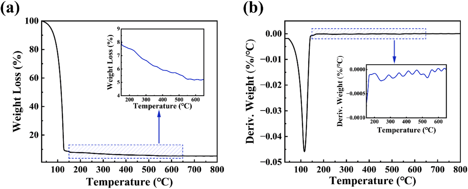
The thermogravimetric (TG) curve of the ZrGdOx precursor is shown in Fig. 2a, which characterizes the conversion process from the precursor solution to the ZrGdOx dry gel. The significant mass loss below 150 °C is attributed to the evaporation of the organic solvent,25 as the boiling point of the solvent used in this experiment is around 120 °C. This is confirmed by the sharp peak at 120 °C in the differential thermogravimetric (DTG) curve in Fig. 2b. Furthermore, the inset of Fig. 2a shows that the weight loss above 150 °C can be expressed as decomposition of the organic ligand and formation of metal–oxygen–metal frameworks, leading to a denser film and reduced impurities.26 There is no significant weight loss above 550 °C, indicating that the precursor solution completes its transformation at about 550 °C. In the inset of Fig. 2b, a smaller peak appears at about 540 °C, indicating the formation of the ZrGdOx lattice. To explore the effect of annealing temperature on the Gd-doped ZrO2 thin films, the samples were annealed at 300, 400, 500, and 600 °C for 1 h in this experiment.
 |
| | Fig. 2 (a) TG and (b) DTG curves of ZrGdOx precursor. | |
3.2 Microstructure analysis
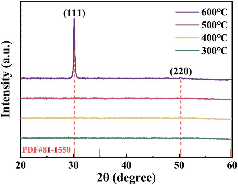
Fig. 3 shows the XRD pattern of ZrGdOx films at different annealing temperatures. As the annealing temperature increases from 300 °C to 500 °C, no diffraction peaks are observed, indicating that the ZrGdOx films remain in the amorphous state. However, when the annealing temperature reaches 600 °C, diffraction peaks appear at 2θ = 30.2° and 50.3° for the ZrGdOx film. According to the PDF#81-1550 card, these two diffraction peaks correspond to the (111) and (220) crystal plane, respectively. It has been reported that pure ZrO2 films typically crystallize at about 450 °C.27 These results clearly indicate that the introduction of an appropriate amount of Gd2O3 into ZrO2 effectively inhibits the crystallization of ZrO2 films, resulting in a delay of at least about 100 °C in the onset of crystallization. This is an exciting result. In future practical production processes, this advantage can be utilized to modify the microstructure of the materials through Gd doping, thereby reducing the gate leakage current of electronic devices and improving their long-term stability. Additionally, it is worth investigating the relationship between the changes in microstructure and the enhancement of dielectric properties. It is well known that for MOS electronic devices, amorphous oxide films are more suitable as gate dielectric layers than crystalline films. This is because crystalline films have a large number of grain boundaries, which act as capture and scattering centers according to the grain boundary charge capture model, leading to high gate leakage currents, reduced insulation, and increased power consumption in the device.28
 |
| | Fig. 3 XRD pattern of ZrGdOx thin films at different annealing temperatures. | |
3.3 Chemical bonding state analysis
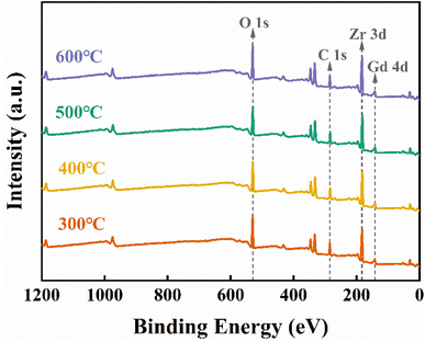
The chemical composition of the ZrGdOx composite films was studied using XPS measurements, as shown in Fig. 4. To avoid experimental errors, all XPS data were charge-shifted and corrected to the binding energy of C 1s at 284.8 eV. Fig. 4 displays the wide-energy-range XPS spectra of all samples with respect to the annealing temperature. It can be noted that the signals of the elements C, O, Zr, and Gd are detected, indicating that the element Gd has been successfully doped into the ZrO2 gate medium. Additionally, no signals from other impurity elements were detected, confirming the absence of contamination.
 |
| | Fig. 4 XPS full spectrum of ZrGdOx thin films. | |
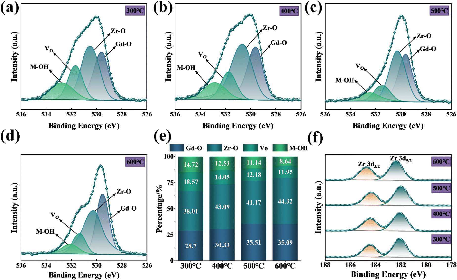
The temperature-dependent XPS spectra of O 1s in ZrGdOx composite films are presented in Fig. 5a–d. The O 1s spectra can be fitted by Gaussian to four subpeaks, centered at 529.58, 530.26, 531.42, and 532.45 eV, respectively. The two subpeaks at 529.58 and 530.26 eV correspond to gadolinium–oxygen bond (Gd–O) and zirconium–oxygen bond (Zr–O), both of which are associated with oxygen in the metal oxide lattice.13,29,30 The subpeak located at 531.42 eV correspond to oxygen vacancies (VO) in the lattice,28 while the subpeak at 532.45 eV is attributed to hydroxyl groups and water adsorbed in air (M–OH).22 To better understand the changes in each oxygen component with annealing temperature in the XPS pattern of O 1s, the specific percentages of each oxygen component were extracted, as shown in Fig. 5e. As the annealing temperature increases from 300 °C to 600 °C, the proportion of metal–oxygen bonds (M–O) in the ZrGdOx composite films increases from 66.71% to 79.41%, enhancing the capacitance and reducing the leakage current. The proportions of VO and M–OH decrease to 11.95% and 8.64%, respectively. These results indicate that high-temperature annealing helps to eliminate oxygen vacancies and enhance dehydroxylation, promoting the conversion of metal hydroxides to metal oxides and forming metal–oxygen frameworks.31 As a gate dielectric layer in CMOS devices, the content of oxygen vacancies and hydroxyl oxygen should be kept as low as possible. This is because these components create trap states in the film's forbidden band, leading to increased gate leakage current and decreased breakdown voltage.32 Therefore, higher-temperature annealing treatment is an effective method to control the content of oxygen vacancies and hydroxyl oxygen, resulting in high-quality films.
 |
| | Fig. 5 O 1s spectra of ZrGdOx films annealed at (a) 300 °C, (b) 400 °C, (c) 500 °C, (d) 600 °C, (e) atomic percentages of the oxygen components in each sample, (f) XPS spectra of Zr 3d. | |
To obtain more information about the chemical bonding states, Fig. 5f shows the evolution of the Zr 3d core energy levels as a function of the annealing temperature. The Zr 3d peaks of all thin film samples were divided into two peaks (Zr 3d3/2 and Zr 3d5/2) with a splitting energy of about 2.4 eV.7 For the ZrGdOx composite films annealed at 300 °C, the centers of the Zr 3d5/2 and Zr 3d3/2 double peaks are located at 182.08 and 184.46 eV, respectively. When the annealing temperature is increased to 500 °C, the centers of the Zr 3d5/2 and Zr 3d3/2double peaks were located at 181.99 and 184.36 eV, respectively, indicating a trend towards lower binding energies. This is attributed to the fact that Zr, with a higher electronegativity than Gd, provides electrons for the Gd–O bond during annealing, generating Gd–O bonds with lower dissociation energy first.13,33 However, as the annealing temperature increases to 600 °C, the Zr 3d double peaks move towards higher binding energies again, with the centers of the Zr 3d5/2 and Zr 3d3/2 double peaks located at 182.36 eV and 184.74 eV, respectively. This phenomenon is attributed to the reaction of Zr and Gd atoms with O atoms at high temperatures to form the ZrGdOx structure.32 Additionally, it is believed that the ZrGdOx composite films crystallize at high temperatures, resulting in a shift of the binding energy to higher direction, which is also consistent with the previous XRD results.34
3.4 Optical characterization and energy band shift analysis
To investigate the optical properties of the ZrGdOx composite films, the optical transmittance of all samples deposited on the quartz substrate with different annealing temperatures was measured as shown in Fig. 6a. The results indicate that all samples exhibit an average optical transmittance of over 80% in the visible region, which implies that ZrGdOx composite films have great potential for applications in transparent electronics. The energy band shift is a critical factor in evaluating the suitability of semiconductor materials for use as high-k gate dielectrics in CMOS devices. Therefore, the valence band (VB) and conduction band (CB) shifts of the ZrGdOx composite films were determined after measuring the energy band gap (Eg).35 According to the light absorption theory, the Eg values of all samples can be determined by Tauc's formula:23where α is the absorption coefficient, hν is the photon energy, A is a constant, and Eg is the optical band gap. The exponent m depends on the type of optical jump between the valence and conduction bands, with m = 1/2 for direct jump and m = 2 for indirect jump. Given that ZrO2 undergoes a direct transition, m should be 1/2, and therefore it is necessary to plot (αhν)2 with respect to hν. The Eg values can be determined by linear extrapolation when (αhν)2 = 0, corresponding to hν = Eg. Fig. 6b illustrates the variation of Eg with different annealing temperatures. As the annealing temperature increases from 300 °C to 600 °C, the Eg values are 5.68, 5.77, 5.87, and 5.92 eV, respectively. The increase in Eg with annealing temperature can be attributed to the reduction in defects and disorder within the films, which decreases the density of localized states in the energy band structure. As a result, the decrease in localized states leads to an increase in Eg.36 Table 1 lists the Eg values of ZrO2 materials involved in recent studies. It can be observed that the Eg of Gd-doped ZrO2 in this experiment is larger than that of pure ZrO2 in previous studies, which is attributed to the d–d coupling of electrons in the Zr 5d and Gd 5d antibonding states.40 Furthermore, among the various doping elements, a moderate amount of Gd exhibits the most significant ability to increase the Eg value of ZrO2.
 |
| | Fig. 6 (a) Transmittance and (b) optical band gaps spectra of ZrGdOx thin films at various annealing temperatures. | |
Table 1 Band gap values of relevant ZrO2 materials in recent years
| Sample |
Experimental variable |
Eg (eV) of pure ZrO2 |
Eg (eV) of the best sample |
Year |
Ref. |
| B-doped ZrO2 |
B-doping concentration |
5.5 |
5.17 |
2015 |
37 |
| ZrO2 |
Annealing temperature |
5.3 |
5.7 |
2016 |
38 |
| Gd-doped ZrO2 |
Gd-doping concentration |
5.65 |
5.83 |
2016 |
13 |
| Y-doped ZrO2 |
Y-doping concentration |
4.91 |
4.92 |
2017 |
39 |
| ZrO2 |
Annealing temperature |
5.8 |
— |
2018 |
18 |
| Al-doped ZrO2 |
Annealing temperature |
5.77 |
5.79 |
2022 |
7 |
| La-doped ZrO2 |
La-doping concentration |
5.68 |
5.71 |
2023 |
22 |
| Gd-doped ZrO2 |
Annealing temperature |
— |
5.87 |
2024 |
This work |
The valence band offset (ΔEv) of the ZrGdOx composite film was determined by measuring the difference in the valence band maximum (VBM) between the dielectric layer and the substrate as follows:41
| | |
ΔEv(ZrGdOx/Si) = Ev(ZrGdOx) − Ev(Si)
| (2) |
where
Ev(ZrGdO
x) is the maximum valence band value of the thin film sample and
Ev(Si) is the maximum valence band value of the Si substrate of 0.5 eV.
Fig. 7a shows the VBM of ZrGdO
x composite films at different annealing temperatures. Using the above
eqn (2), the Δ
Ev values for the samples annealed at 300, 400, 500, and 600 °C can be obtained as 2.02, 2.08, 2.13, and 2.37 eV, respectively.
 |
| | Fig. 7 (a) Valence band spectra of ZrGdOx thin films, (b) schematic energy bands of ZrGdOx/Si gate stacks. | |
The conduction band offset (ΔEc) for all samples can be determined by the difference between the band gap values of the films and the ΔEv, the band gap value of Si substrate, using the following eqn (3):
| | |
ΔEc(ZrGdOx/Si) = Eg(ZrGdOx) − ΔEv(ZrGdOx/Si) − Eg(Si)
| (3) |
where
Eg(ZrGdO
x) and
Eg(Si) are the bandgap values of the thin films and the Si substrate, respectively. The Δ
Ec values are calculated to be 2.54, 2.57, 2.62, and 2.43 eV for the samples annealed at 300, 400, 500, and 600 °C, respectively. Based on the above calculations,
Fig. 7b schematically illustrates the energy bands and energy band offsets for the ZrGdO
x/Si gate-stacked structures at different annealing temperatures. It can be noticed that all Δ
Ev and Δ
Ec values exceed 1 eV, with the sample annealed at 500 °C showing the largest Δ
Ec value. A sufficiently large barrier height is crucial for blocking electrons and holes, inhibiting carrier transport, and reducing gate leakage current, making the ZrGdO
x composite films annealed at 500 °C suitable for practical applications.
3.5 Micro-morphological analysis
Fig. 8a displays the SEM cross sections of the ZrGdOx composite thin films after different annealing heat treatments. The SEM images reveal a distinct demarcation between the thin film and the Si substrate. After measuring the actual film thicknesses, the ZrGdOx composite films annealed at 300, 400, 500, and 600 °C had thicknesses of approximately 38.9, 38.6, 39.4, and 39.1 nm, respectively. These measurements are crucial for calculating the electrical parameters of MOS capacitors. For CMOS devices, performance is highly dependent on the surface quality of the gate dielectric film.
 |
| | Fig. 8 (a) Cross-sectional SEM patterns of ZrGdOx thin films, (b) 2D and (c) 3D AFM maps of the samples at different annealing temperatures, respectively. | |
Fig. 8b and c present the 2D and 3D AFM patterns of the ZrGdOx composite films at different annealing temperatures, with a scanning range of 2 × 2 μm. The root-mean-square (RMS) roughness values of the films annealed at 300, 400, 500, and 600 °C were 0.219, 0.189, 0.154, and 0.310 nm, respectively. The average RMS value of the ZrGdOx composite films prepared in the current work was only 0.218 nm, indicating that the films were uniformly smooth. This is inextricably linked to the UV ozone-assisted treatment process, as it has been shown that a suitable UV ozone treatment time can effectively clean the oxide surface.42 As the annealing temperature increased from 300 °C to 500 °C, the RMS values continued to decrease, likely due to the removal of residual organic groups and the formation of a dense metal oxide framework. However, the RMS value of the sample annealed at 600 °C was higher than the others, which was attributed to the fact that this temperature induced crystallinity and degraded film quality, as confirmed by XRD results.43 Maintaining a smooth and uniform surface in ZrGdOx composite films as gate dielectrics is essential to minimize interfacial trap density and carrier scattering centers. In this paper, the surface smoothness of the films prepared using the UV ozone-assisted solution method is comparable to that of films produced by magnetron sputtering and atomic layer deposition.44,45
3.6 Electrical characterization
To evaluate the electrical characteristics of the ZrGdOx composite films as gate dielectrics, MOS capacitors with the structure of Al/ZrGdOx/Si were fabricated. Fig. 9a presents typical C–V characteristic curves at high frequency (1 MHz) for MOS capacitors based on ZrGdOx composite films annealed at different temperatures. All samples were scanned from a gate voltage of −4 V to +4 V and then inversely, to determine their hysteresis. According to Fig. 9a, the ZrGdOx composite films annealed at 300, 400, 500, and 600 °C exhibited cumulative capacitances (Cox) of 466, 609, 660, and 528 pF, respectively, at a gate voltage of +4 V. The dielectric constant (k) and the equivalent oxide thickness (EOT) of the ZrGdOx composite films can be calculated using the following eqn (4) and (5):| |
 | (4) |
| |
 | (5) |
where Cox is the cumulative capacitance of the sample, d is the actual physical thickness of the film, ε0 is the vacuum dielectric constant, A is the area of the Al electrode, and kSiO2 is the dielectric constant of SiO2. The k values of the ZrGdOx composite films annealed at 300, 400, 500, and 600 °C were calculated to be 13.5, 17.5, 19.3, and 15.3, respectively. Additionally, the EOT values of these films were 11.2, 8.6, 8.0, and 9.9 nm, respectively. For the sample annealed at 500 °C, the smallest EOT (8.0 nm) and the largest k value (19.3) were obtained. Notably, as the annealing temperature increased to 500 °C, the EOT decreased continuously, and the k value increased. However, when the annealing temperature was raised to 600 °C, the EOT suddenly increased and the k value decreased. Two possible reasons for this phenomenon are: first, the reaction between the ZrGdOx composite film and the Si substrate during high-temperature annealing, which generates a low-k interfacial layer, increasing the EOT and decreasing the k value. The second reason could be the degradation of the interfacial quality at higher annealing temperatures, confirmed by AFM data.
 |
| | Fig. 9 (a) C–V and (b) J–V curves of the MOS capacitors based on ZrGdOx films. | |
Furthermore, the flat-band capacitance (Cfb) of the ZrGdOx composite films annealed at 300, 400, 500, and 600 °C can be calculated, and the flat-band voltage (Vfb), and hysteresis (ΔVfb) can be determined sequentially from the C–V curves. In addition, the equivalent oxide charge density (Qox), and the boundary trap oxide charge density (Nbt) can be calculated by the following eqn (6)–(8):46
| |
 | (6) |
| |
 | (7) |
| |
 | (8) |
where
k is the dielectric constant of the ZrGdO
x composite film,
εrs is the dielectric constant of the Si substrate,
d is the actual physical thickness of the ZrGdO
x composite film,
K is Boltzmann's constant,
T = 300 K,
ε0 is the vacuum dielectric constant,
NA is the carrier concentration,
φms is the difference between the work function of the Al electrode and the Si substrate,
A is the area of the Al electrode, and
q is the charge of the electron.
The detailed electrical parameters are shown in Table 2. The Vfb is always positive, indicating the presence of negative trap charge in the film, which may originate from OH− in the residual organic solvent in the dielectric.23 Additionally, the absolute value of Vfb decreases with increasing annealing temperature, and the Qox obtained from Vfb decreases from 1.76 × 1012 cm−2 to 5.64 × 1011 cm−2, suggesting that the films at higher annealing temperature contain fewer defects and traps. From Table 2, it can be clearly seen that the ZrGdOx composite film annealed at 500 °C exhibits the smallest ΔVfb (0.01 V), indicating a minimum of oxide trapping charge in the films. Since Nbt depends on ΔVfb in a certain degree, the sample annealed at 500 °C has the smallest Nbt (6.5 × 1010 cm−2) by rigorous calculation.
Table 2 Specific electrical parameters of the MOS capacitors
| Sample |
Cox (pf) |
EOT (nm) |
k |
Cfb (pf) |
Vfb (V) |
ΔVfb (V) |
Qox (cm−2) |
Nbt (cm−2) |
| 300 °C |
466 |
11.2 |
13.5 |
211.5 |
0.72 |
0.22 |
1.76 × 10¹² |
4.2 × 10¹¹ |
| 400 °C |
609 |
8.6 |
17.5 |
236.7 |
0.49 |
0.02 |
1.73 × 10¹² |
5.0 × 10¹⁰ |
| 500 °C |
660 |
8.0 |
19.3 |
244.5 |
0.26 |
0.01 |
1.25 × 10¹² |
2.7 × 10¹⁰ |
| 600 °C |
528 |
9.9 |
15.3 |
224.0 |
0.06 |
0.03 |
5.64 × 10¹¹ |
6.5 × 10¹⁰ |
Fig. 9b illustrates the J–V characteristic curves of the MOS capacitor with structure Al/ZrGdOx/Si. It is evident that the J–V curves are asymmetric about 0 V, attributed to the different carrier supply under different gate voltage injection modes. Different energy bands in these injection modes result in a much smaller leakage current density under substrate injection compared to gate injection for the same absolute gate voltage value.47 The composite film annealed at 500 °C exhibited the lowest leakage current density (9.61 × 10⁻⁶ A cm2) at a gate voltage of 1 V. However, when the annealing temperature was increased to 600 °C, the leakage current density of the sample drastically increased to, attributed to microstructural alteration, interfacial quality deterioration, and defect increases. In conclusion, the composite film annealed at 500 °C demonstrated the best electrical properties.
Table 3 lists the best dielectric properties of some high-k materials in recent years, comparing them with the dielectric parameters of the composite films annealed at 500 °C in this work. It is found that compared to expensive and complex process methods, the gate dielectric films prepared by UVO-assisted sol–gel method, which is a simple and efficient approach, exhibit better electrical properties than other gate dielectrics. And this is a promising result. Therefore, the excellent dielectric properties of the gate dielectric films, combined with the facile and low-cost preparation process, offer great potential for the future development of low-cost and high-performance MOS devices.
Table 3 Electrical parameters of different high-k dielectric materials reported in recent years
| High-k materials |
Preparation method |
Annealing temperature |
Dielectric constant (k) |
Leakage current (A cm−2) |
Year |
Ref. |
| B-doped |
Sol–gel |
150 °C |
10.5 |
9.1 × 10⁻⁵ |
2015 |
37 |
| Ti-doped |
Sputtering |
— |
39.92 |
1.39 × 10⁻⁵ |
2016 |
48 |
| Gd-doped |
Sol–gel |
400 °C |
11.4 |
— × 10−6 |
2017 |
49 |
| Y-doped |
Sputtering |
600 °C |
11.28 |
9.69 × 10⁻⁴ |
2018 |
16 |
| Sputtering |
600 °C |
21.2 |
4.94 × 10⁻³ |
2019 |
32 |
| Al-doped |
ALD |
200 °C |
8.1 |
6.2 × 10⁻⁷ |
2020 |
50 |
| Sputtering |
430 °C |
— |
0.79 × 10⁻⁴ |
2021 |
51 |
| La-doped |
Sol–gel |
500 °C |
11.5 |
6.3 × 10⁻⁶ |
2023 |
22 |
| Gd-doped |
Sol–gel |
500 °C |
19.3 |
9.61 × 10⁻⁶ |
2024 |
This work |
3.7 Leakage current mechanism analysis
Since gate leakage current increases the power consumption of electronic devices, the leakage current mechanism was analyzed for composite films annealed at 500 °C to better understand the generation of leakage current. Due to the complexity of leakage current conduction in thin films, this paper mainly analyzes the leakage current using three conduction mechanisms: ohmic conduction, Schottky emission (SE), and Pool–Frenkel (P–F). In Fig. 10a, a good linear relationship between J and E is observed in the field strength range of 0.08 < E < 0.37 MV cm−1, indicating that ohmic conduction is the dominant conduction mechanism in this range. Ohmic conduction occurs due to the movement of free particles in the conduction or valence bands of the dielectric at low voltages. Fig. 10b shows a good linear relationship between and E1/2 within a field strength range of, indicating that Schottky emission is the dominant conduction mechanism in this range. Schottky emission results from thermal excitation, which provides electrons with energy sufficient to overcome the potential barrier between the Si substrate and the dielectric, allowing them to enter the gate dielectric layer. From Fig. 10c, it is observed that in the field strength range of in the middle to high electric field strength, the P–F emission satisfies the linear relationship between E1/2 and, indicating that P–F conduction is dominant at this time. In conclusion, the leakage current conduction mechanism of ZrGdOx composite films annealed at 500 °C transitions from ohmic conduction to Schottky emission to Pool–Frenkel emission as the electric field strength increases.
 |
| | Fig. 10 (a) Ohmic conduction, (b) SE emission, and (c) P–F emission plots of Al/ZrGdOx/Si capacitors in substrate injection mode. | |
4. Conclusion
ZrGdOx composite films were successfully prepared on n-type Si substrates using UVO-assisted sol–gel method. The annealing temperature range of the ZrGdOx composite films was first determined through TG analysis. Subsequently, the effects of different annealing temperatures on the microstructure, chemical bonding state, optical properties, surface morphology, and electrical properties of the ZrGdOx composite films were investigated by using XRD, XPS, UV-vis, SEM, AFM, and semiconductor analyzers. The XRD results showed that doping with Gd element increased the crystallization temperature of the ZrO2 films. Additionally, the ZrGdOx composite films heat-treated at 500 °C remained in an amorphous state, which is ideal for use as a gate insulating layer in CMOS device. XPS analysis revealed that at 500 °C, the ZrGdOx composite films had a relatively high proportion of M–O bonds (76.68%) and low proportions of VO (12.18%) and M–OH (11.14%), indicating that this annealing temperature can promote the formation of a dense metal–oxygen framework. The optical transmittance and band gap values of the ZrGdOx composite films at various heat treatment temperatures were obtained via UV-vis spectroscopy, and the energy band shifts were determined combined from the valence band spectra. The sample annealed at 500 °C exhibited a large band gap value (Eg = 5.87 eV) and conduction band offset (ΔEc = 2.62 eV), which helps to suppress carrier transport and leakage current generation. The AFM results indicated that the thin films, treated with UV ozone, had smooth surfaces with RMS values as low as 0.154 nm. The MOS capacitor with the structure Al/ZrGdOx/Si was tested and analyzed, revealing that the gate dielectric film exhibited the best electrical properties when the annealing temperature was 500 °C. At this temperature, the film had the highest dielectric constant (k = 19.3), the smallest boundary trap oxide charge density (Nbt = 2.7 × 1010 cm−2), the smallest hysteresis (ΔVfb = 0.01 V), and the lowest gate leakage current density (J = 9.61 × 10⁻⁶ A cm−2). Finally, the leakage current mechanism was analyzed for a MOS capacitor with a 500 °C annealed ZrGdOx composite film as the gate dielectric layer. The leakage current conduction mechanisms were found to be Ohmic conduction, Schottky emission, and Pool–Frenkel conduction at low, medium, and medium–high electric field strengths, respectively.
Data availability
The data supporting the findings of this study are available from the corresponding author upon reasonable request.
Author contributions
Chaozhong Guo: data curation (lead); formal analysis (lead); investigation (lead); methodology (lead); writing – original draft (lead); writing – review & editing (lead). Kamale Tuokedaerhan: supervision (lead); resources (lead); conceptualization (lead); funding acquisition (lead). Xiangqian Shen: methodology (supporting). Yerulan Sagidolda: resources (supporting). Zhambyl Azamat: resources (supporting).
Conflicts of interest
There are no conflicts to declare.
Acknowledgements
This study was financially supported by the Natural Science Foundation of Xinjiang Uygur Autonomous Region (Grant No. 2021D01C035).
References
- J. Robertson and R. M. Wallace, Mater. Sci. Eng., 2015, 88, 1–41 CrossRef
 .
. - M. M. Waldrop, Nature, 2016, 530, 144–147 CrossRef .
- J. H. Choi, Y. Mao and J. P. Chang, Mater. Sci. Eng., 2011, 72, 97–136 CrossRef .
- J.-J. Huang, L.-T. Huang, M.-C. Tsai, M.-H. Lee and M.-J. Chen, Appl. Surf. Sci., 2014, 305, 214–220 CrossRef .
- Y. Gong, K. Zhao, L. Yan, W. Wei, C. Yang, H. Ning, S. Wu, J. Gao, G. Zhou, X. Lu and J.-M. Liu, IEEE Electron Device Lett., 2018, 39, 280–283 Search PubMed .
- H.-C. You, C.-M. Chang, T.-F. Liu, C.-C. Cheng, F.-C. Chang and F.-H. Ko, Appl. Surf. Sci., 2012, 258, 10084–10088 CrossRef .
- H. Cai, K. Tuokedaerhan, Z. Lu, R. Zhang and H. Du, Coatings, 2022, 12, 1837 CrossRef .
- X. Zhao, S. Wang, A. Li, J. Ouyang, G. Xia and J. Zhou, RSC Adv., 2014, 4, 14890–14895 RSC .
- D. Kumar, A. Singh, N. Kaur, A. Thakur and R. Kaur, SN Appl. Sci., 2020, 2, 644 CrossRef .
- S. Wang, S. Yao, J. Lin and G. Xia, Ceram. Int., 2019, 45, 9829–9834 CrossRef CAS .
- M. K. Hossain, M. H. Ahmed, M. I. Khan, M. S. Miah and S. Hossain, ACS Appl. Electron. Mater., 2021, 3, 4255–4283 CrossRef .
- S. Li, Y. Lin, S. Tang, L. Feng and X. Li, J. Rare Earths, 2021, 39, 121–128 Search PubMed .
- D. Q. Xiao, G. He, J. G. Lv, P. H. Wang, M. Liu, J. Gao, P. Jin, S. S. Jiang, W. D. Li and Z. Q. Sun, J. Alloys Compd., 2017, 699, 415–420 CrossRef .
- W. Liu, G. He, D. Wang, H. Yu, Q. Gao, Y. Liu and Z. Fang, IEEE Trans. Electron Device, 2022, 69, 242–247 Search PubMed .
- I. Sadeghi, K. Ye, M. Xu, Y. Li, J. M. LeBeau and R. Jaramillo, Adv. Funct. Mater., 2021, 31, 2105563 CrossRef .
- S. Liang, G. He, D. Wang, L. Hao, M. Zhang and J. Cui, ACS Omega, 2019, 4, 11663–11672 CrossRef PubMed .
- H. Liang, B. Zhang, D. Zhou, X. Guo, Y. Li, Y. Lu and Y. Guo, Ceram. Int., 2021, 47, 12137–12143 Search PubMed .
- M. H. Boratto, M. Congiu, S. B. O. Dos Santos and L. V. A. Scalvi, Ceram. Int., 2018, 44, 10790–10796 CrossRef .
- W. Xu, J. Jiang, L. Han and X. Feng, Ceram. Int., 2020, 46, 17295–17299 CrossRef .
- Y. Shi, G. Liu, X. Wu, C. Zhou, C. Yang, Z. Yang and F. Shan, IEEE Trans. Electron Devices, 2024, 71, 2789–2793 Search PubMed .
- X. Dong, G. Xia, Q. Zhang, L. Li, H. Gong, J. Bi and S. Wang, Ceram. Int., 2017, 43, 15205–15213 CrossRef .
- H. Cai, K. Tuokedaerhan, Z. Lu, R. Zhang and H. Du, Vacuum, 2023, 217, 112542 CrossRef .
- D. Q. Xiao, G. He, M. Liu, J. Gao, P. Jin, S. S. Jiang, W. D. Li, M. Zhang, Y. M. Liu, J. G. Lv and Z. Q. Sun, J. Alloys Compd., 2016, 688, 252–259 CrossRef .
- L. Zhu, G. He, J. Lv, E. Fortunato and R. Martins, RSC Adv., 2018, 8, 16788–16799 RSC .
- G. Xia and S. Wang, Ceram. Int., 2019, 45, 16482–16488 CrossRef .
- J. H. Park, Y. B. Yoo, K. H. Lee, W. S. Jang, J. Y. Oh, S. S. Chae and H. K. Baik, ACS Appl. Mater. Interfaces, 2013, 5, 410–417 CrossRef CAS .
- H. Cai, K. Tuokedaerhan, Z. Lu, H. Du and R. Zhang, Phys. Status Solidi A, 2023, 220, 2200903 CrossRef CAS .
- G. He, W. Li, Z. Sun, M. Zhang and X. Chen, RSC Adv., 2018, 8, 36584–36595 RSC .
- G. He, J. Zhang, Z. Sun, J. Lv, H. Chen and M. Liu, AIP Adv., 2016, 6, 025003 CrossRef .
- X. Wang, X. Zhang, Y. Xiong, J. Du, M. Yang and L. Wang, Rare Metals, 2011, 30, 647–650 CrossRef CAS .
- C. Fan, A. Liu, Y. Meng, Z. Guo, G. Liu and F. Shan, IEEE Trans. Electron Devices, 2017, 64, 4137–4143 CAS .
- S. Li, Y. Wu, H. Yu, K. Fu, J. Zheng, X. Li and W. Tian, J. Alloys Compd., 2019, 791, 839–846 CrossRef CAS .
- X.-H. Zhao, J. Zhuang, Q.-J. Sun, Z. Tang, X.-G. Tang and V. A. L. Roy, J. Alloys Compd., 2023, 952, 170062 CrossRef CAS .
- L. Zhu, G. He, W. Li, B. Yang, E. Fortunato and R. Martins, Adv. Electron. Mater., 2018, 4, 1800100 CrossRef .
- Y. Y. Zhu, S. Chen, R. Xu, Z. B. Fang, J. F. Zhao, Y. L. Fan, X. J. Yang and Z. M. Jiang, Appl. Phys. Lett., 2006, 88, 162909 CrossRef .
- A. Liu, G. Liu, H. Zhu, H. Song, B. Shin, E. Fortunato, R. Martins and F. Shan, Adv. Funct. Mater., 2015, 25, 7180–7188 CrossRef CAS .
- D. Q. Xiao, G. He, P. Jin, J. Gao, J. W. Zhang, X. F. Chen, C. Y. Zheng, M. Zhang and Z. Q. Sun, J. Alloys Compd., 2015, 649, 1273–1279 CrossRef CAS .
- C. Zhu, A. Liu, G. Liu, G. Jiang, Y. Meng, E. Fortunato, R. Martins and F. Shan, J. Mater. Chem. C, 2016, 4, 10715–10721 RSC .
- B.-E. Park, I.-K. Oh, C. Mahata, C. W. Lee, D. Thompson, H.-B.-R. Lee, W. J. Maeng and H. Kim, J. Alloys Compd., 2017, 722, 307–312 CrossRef CAS .
- Y. Xiong, H. Tu, J. Du, M. Ji, X. Zhang and L. Wang, Appl. Phys. Lett., 2010, 97, 012901 CrossRef .
- R. Ma, M. Liu, G. He, M. Fang, G. Shang, J. Zhang, X. Chen, J. Gao, G. Fei and L. Zhang, J. Alloys Compd., 2015, 646, 310–314 CrossRef CAS .
- M.-J. Lee, T. I. Lee, J.-H. Cho, W. Lee and J.-M. Myoung, Mater. Sci. Semicond. Process., 2015, 30, 469–475 CrossRef .
- A. Liu, G. Liu, H. Zhu, Y. Meng, H. Song, B. Shin, E. Fortunato, R. Martins and F. Shan, Curr. Appl. Phys., 2015, 15, S75–S81 CrossRef .
- Y. Xu, H. Chen, H. Xu, M. Chen, P. Zhou, S. Li, G. Zhang, W. Shi, X. Yang, X. Ding and B. Wei, ACS Appl. Mater. Interfaces, 2023, 15, 16874–16881 CrossRef .
- Z. Han, J. Han and A. Abliz, Appl. Surf. Sci., 2024, 648, 158995 CrossRef .
- P. Jin, G. He, Z. B. Fang, M. Liu, D. Q. Xiao, J. Gao, S. S. Jiang, W. D. Li, Z. Q. Sun and M. Zhang, Ceram. Int., 2017, 43, 3101–3106 CrossRef .
- Z. Xu, M. Houssa, S. De Gendt and M. Heyns, Appl. Phys. Lett., 2002, 80, 1975–1977 CrossRef .
- S. S. Jiang, G. He, J. Gao, D. Q. Xiao, P. Jin, W. D. Li, J. G. Lv, M. Liu, Y. M. Liu and Z. Q. Sun, Ceram. Int., 2016, 42, 11640–11649 CrossRef .
- W. D. Li, G. He, C. Y. Zheng, S. Liang, L. Zhu and S. S. Jiang, J. Alloys Compd., 2018, 731, 150–155 CrossRef .
- Dharmender and K. Nigam, Silicon, 2021, 13, 2347–2356 CrossRef .
- G. Arun Kumar Thilipan and A. Rao, Mater. Sci. Semicond. Process., 2021, 121, 105408 CrossRef .
|
| This journal is © The Royal Society of Chemistry 2025 |
Click here to see how this site uses Cookies. View our privacy policy here. 
 Open Access Article
 This Open Access Article is licensed under a
  *ab,
Xiangqian Shenab,
Yerulan Sagidoldac and
Zhambyl Azamatc
*ab,
Xiangqian Shenab,
Yerulan Sagidoldac and
Zhambyl Azamatc