
 Open Access Article
 This Open Access Article is licensed under a Creative Commons Attribution-Non Commercial 3.0 Unported Licence
Multi-head spatial atomic layer deposition: a robust approach for precise doping and nanolaminate fabrication in open-air environments†
Hayri Okcu *ab,
Martin Ignacio Broensa,
Vijaya Shanthi Paul Raja,
Pia Javiera Vasquez Riveraa,
Gustavo Ardilab and
David Muñoz-Rojas*a
*ab,
Martin Ignacio Broensa,
Vijaya Shanthi Paul Raja,
Pia Javiera Vasquez Riveraa,
Gustavo Ardilab and
David Muñoz-Rojas*a
aUniv. Grenoble Alpes, CNRS, Grenoble INP, LMGP, 38000 Grenoble, France. E-mail: hayri.okcu@grenoble-inp.fr; david.munoz-rojas@grenoble-inp.fr
bUniv. Grenoble Alpes, Univ. Savoie Mont Blanc, CNRS, Grenoble INP, CROMA, 38000, Grenoble, France
First published on 11th July 2025
Abstract
Open-air manufacture of functional nanolaminates demands rapid and scalable methods that maintain nanoscale precision across individual layers. Conventional spatial atomic layer deposition (SALD) employs a single deposition head, and the concurrent exposure to mutually reactive precursors does not provide precise layer thickness accuracy nor sharp interfaces. This work addresses these challenges with an innovative multi-head SALD design. In this study, we introduced a novel multi-head SALD system comprising a uniform head for depositing 5 nm zinc oxide (ZnO) sublayers, while a combinatorial high-throughput head delivered wedge-like thickness gradient in aluminum oxide (Al2O3) sublayers, increasing gradually from 0 to approximately 6 nm along the substrate. Eight ZnO/Al2O3 bilayers (320 ALD cycles per material) were completed in open air at 200 °C. Transmission electron microscopy recorded highly sharp and reproducible layer-to-layer structures with thickness deviations of 0.3 nm; X-ray photoelectron spectroscopy verified the absence of undesirable aluminum contamination in the reference ZnO regions. With increasing Al2O3 thickness, surface roughness was reduced from 0.58 to 0.33 nm, ZnO (002) reflections broadened as crystallite size was confined, and Kelvin probe measurements showed a shift in work function values from 4.75 to 4.35 eV with Al2O3 passivation. This study demonstrates that the multi-head SALD method offers a robust platform for achieving precise multilayer control in open-air conditions, thereby paving the way for further innovations in materials research through optimized experimental conditions and combinatorial approaches.
Introduction
With technological advancement, there is growing demand for time- and cost-effective methods to fabricate high-quality materials. Zinc oxide (ZnO) and aluminum oxide (Al2O3) nanolaminates are layered structures that exhibit optical, electrical, and mechanical properties derived from the combined characteristics of both materials. ZnO, known for its wide bandgap, offers semiconducting properties,1 a wurtzite structure exhibits a built-in polarization and piezoelectric response,2 and a high exciton binding energy,3 making it suitable for photonic and electronic devices.4 Al2O3, on the other hand, is recognized for its high dielectric strength and stability,5 thereby enhancing the protective and insulating capabilities of the composite. Recent studies suggest that engineering the thickness of ZnO and Al2O3 layers in ZnO/Al2O3 nanolaminates offers great tuneability across multiple properties, including mechanical characteristics such as fracture resistance,6 hardness and toughness,7 dielectric properties,8,9 charge storage,10 work function,11 bandgap,12,13 luminescent behaviors and efficacy,11,14–16 thermal conductivity,17 photocatalytic efficiency,18 gas permeability,6 and optical transparency.13,19 Therefore, ZnO/Al2O3 nanolaminates have been extensively studied for applications such as dielectric barriers, transparent conducting coatings, and optoelectronic components, including solar cells and ultraviolet detectors.11,20These nanolaminates are often synthesized through atomic layer deposition (ALD), which enables precise control over thickness, composition, and uniformity at the atomic scale.21 ALD stands out as a powerful technique due to its ability to achieve nanoscale thickness precision and high conformality. The time-resolved, sequential nature of ALD allows precise control over reaction kinetics, the incorporation of dopants, surface treatments, and in situ characterization, making it a unique tool in materials research. However, a key limitation of ALD is its slow deposition rate.22 Additionally, conventional ALD systems typically require a chamber and a vacuum system to ensure effective purging, which increases operational costs and complicates maintenance. There is, therefore, a significant gap in the literature regarding open-air direct deposition of nanolaminates. According to our present knowledge, the only reported instance of open-air ZnO/Al2O3 deposition, not involving ALD, was conducted by Gonullu utilizing a spray-pyrolysis technique.18 That work exhibited a single bilayer ZnO/Al2O3 with a film thickness variation between 500 nm to 1 μm. It also revealed a considerable diffusion of Al into the ZnO matrix, resulting in a lack of sharp interfaces. This falls far short of reaching the controlled features obtained with ALD.
To overcome these limitations, atmospheric-pressure spatial atomic layer deposition (AP-SALD) has emerged as a promising alternative. Conventional SALD setups employ a spatially sequenced injector configuration, in which gas injectors are integrated into the deposition head. This arrangement enables the sequential exposure of the substrate to different precursors as it moves through the respective zones.23,24 Unlike ALD, close-proximity SALD directly targets the substrate with precursors to create localized and reduced reaction zones, which provides two key advantages. First, enhanced mass transport efficiency allows operation in open-air environments without requiring a (vacuum) chamber. This enables continuous deposition processes suitable for large-area applications, such as roll-to-roll (R2R) systems. Second, it reduces the required time for surface saturation and purging per ALD step, which significantly increases the deposition rate—up to 100 times faster than traditional ALD.24–26 Additional advantages of reduced reaction zones include lower precursor consumption and a reduced heating zone, making SALD a more sustainable and environmentally friendly gas-phase deposition technique.27,28 The efficiency of SALD has drawn considerable interest from both industrial and academic sectors, further reinforcing its appeal for industrial-scale production.
When using a close-proximity SALD approach, deposition quality depends strongly on the head geometry design. Many studies have suggested improvements in head design to reduce intermixing and prevent unwanted chemical vapor deposition (CVD) reactions, often guided by computational simulations.26,29,30 Despite these efforts, careful optimization of deposition parameters such as substrate speed, deposition temperature, bubbler temperatures, gas flow rates for each SALD head design and the selection of suitable precursor chemistry is still required. Finding the optimal deposition conditions can easily demand considerable time and effort. Consequently, combinatorial synthesis methods have emerged as a highly efficient strategy to deposit samples under varying deposition parameters (e.g., flow rate,31 deposition temperature,32 and others33) on a single sample. Another significant challenge in SALD is the controlled usage of different metal precursors for doping or nanolaminates, which is crucial for adjusting electrical properties, carrier mobility, optical characteristics such as band gap, and structural features like defect density and grain boundaries.34,35 The most common multi-precursor approach in SALD involves co-dosing, where two precursors are mixed in a manifold. While co-dosing is often presumed to enable isotropic mixing without significant precursor competition, in practice, it frequently results in unintended cross-reactions and the formation of undesirable by-products. The precursors for metal oxides and metal nitrides may interact in ways that hinder the desired growth. For example, Lancaster et al. highlighted the difficulty of growing Zn(O,S) thin films for tuneable band gaps with controlled sulphur content due to a significant surface exchange reaction between ZnO and H2S, which makes achieving the desired composition and homogeneity challenging.36 Additionally, temporarily separated co-dosing tends to produce more mixed or alloyed layers, making it difficult to obtain sharp interfaces between layers, such as in dielectric or barrier stacks, thereby rendering this method unsuitable for producing complex multilayer or composite film structures where precursor control over layer composition and thickness is required.37 This mixed exposure of precursors also risks undermining the sequentiality of ALD (one of the key merits of ALD)—namely, the capability to achieve controlled, uniform, and self-limiting film growth.Precursor mixing introduce variability in dopant incorporation and potentially degrade the desired material properties, as also discussed by Macco and Kessels.38 Under these conditions, the super-cycle approach—where precursors are pulsed sequentially—provides a more reliable solution for ALD processes by offering improved control over material composition and interface sharpness. Consequently, this method is frequently employed for the deposition of nanolaminates39 and applications requiring precise doping control, such as aluminium-doped ZnO (AZO).40
In this work, we demonstrate a precisely controlled multi-precursor usage through a multi-head SALD set-up in open-air. In comparison with conventional mono-head SALD setups,41 the proposed configuration provides enhanced thickness control and eliminates undesired cross-contamination. The proof-of-concept is demonstrated by the deposition of ZnO/Al2O3 nanolaminates. We demonstrate the versatility of our approach by exploiting two separate deposition heads: the ZnO sublayer is deposited using a standard uniform deposition head, while a custom-designed combinatorial high-throughput (CHT) head is employed for Al2O3 layer deposition, thereby generating a wedge-like Al2O3 thickness gradient ranging from 0 to approximately 6 nm in each layer.33 Comprehensive characterizations demonstrate precise control over the bulk properties as the Al2O3 sublayer thickness increases, and precise elemental analyses confirm the absence of Al contamination, with structural characterizations revealing highly sharp layer interfaces and reproducible thickness control in a few nanometer precision. Overall, the proposed multi-head SALD approach exhibits significant potential for the facile fabrication of controlled doping and multilayer film structures in open-air, thereby broadening the scope of high-throughput material studies with enhanced controllability.
Experimental methods
Film depositions were conducted using a custom-built AP-SALD system. Diethylzinc (DEZ, Zn(C2H5)2) was used as the zinc precursor, while trimethylaluminium (TMA, Al(CH3)3) served as the aluminium precursor. Ultrapure water (H2O) was used as the co-reactant. Both DEZ, TMA, and H2O bubblers were contained at room-temperature during the deposition process. Nitrogen gas was employed as both the carrier and barrier gas throughout the deposition. Two distinct deposition heads were utilized: one with a uniform metal flow channel for DEZ and another with a combinatorial channel for TMA. Each head was equipped with one metal channel, two water channels, and six nitrogen channels, the latter functioning as both a barrier and purging mechanism. For ZnO deposition, flow rates per channel were: 20 sccm DEZ (bubbler), 100 sccm N2 (DEZ dilution), 30 sccm H2O (bubbler), 60 sccm N2 (H2O dilution), and 100 sccm N2 (barrier). For Al2O3 deposition, flow rates per channel were: 10 sccm TMA (bubbler), 100 sccm N2 (TMA dilution), 30 sccm H2O (bubbler), 30 sccm N2 (H2O dilution), and 300 sccm N2 (barrier). The substrate-to-head gap was set to 150 μm using a feeler gauge. Highly p-type doped silicon (Si) (100) wafers with an approximately 2 nm native oxide layer (BT Electronics) were used as substrates. Depositions were performed at a temperature of 200 °C. The process involved 40 ALD cycles each for ZnO and Al2O3 films, repeated over eight super-cycles, resulting in a total of 320 ALD cycles per material. Substrate speeds were adjusted according to the precursor: 5.23 cm s−1 for the ZnO head and 7.85 cm s−1 for the Al2O3 head.A custom SALD deposition head was designed with computer-aided tools (Autodesk Fusion) and manufactured with a stereolithography (SLA) printer (Formlabs 2) to facilitate combinatorial high-throughput (CHT) film growth for Al2O3 layers and accelerate the optimization of material properties. The substrate was positioned 150 μm below this channel to form a confined space for precursor flow (10 sccm). Computational fluid dynamics (CFD) simulations were performed using COMSOL Multiphysics 5.5 to analyze the gas flow and precursor distribution. A three-dimensional representation of the reactor head was used, and the model of laminar flow and transport of diluted species was applied based on the established low-Reynolds-number conditions inside the SALD reactor. The resulting predictions guided the design by indicating how variations in channel width influence local precursor delivery across the substrate surface. The detailed information for the CFD simulation parameters is given in the ESI.† The thickness of the films was estimated using a FilmSense FS-1 Spectroscopic Ellipsometer. The associated Cauchy model employed for these measurements is provided in the ESI.† For roughness measurements, an atomic force microscope (AFM) was employed. A Bruker Dimension Icon AFM microscope was utilized, operating with platinum-coated silicon probes (PtSi-NCH, from Nanosensors) for the scanning process. Height sensor data were acquired from a 500 nm × 500 nm area, with the scan speed adjusted to 1 Hz (corresponding to a tip speed of 1 μm s−1) and 256 samples per line scan. Furthermore, the NanoScope Analysis software of Bruker was utilized to extract the three-dimensional AFM images and roughness values.
The crystallinity of the deposited films was examined using a Rigaku Smartlab X-ray Diffractometer (XRD) equipped with a copper X-ray source configured in a grazing-incidence geometry at 0.34° incidence angle. A 2Theta scan was conducted at 45 kV to ensure a sufficiently energetic beam for inducing diffraction while maintaining a parallel beam alignment to reduce geometric aberrations.42 The horizontal Soller slit was set at 2.5° to control beam divergence, and a 2.0 mm mask was employed to enhance signal quality and minimize background scattering. The diffracted beam then passed through a vertically parallel slit analyzer (PSA) of 0.5° and a horizontal PSA of 5.0°, thereby refining the scattering profile and improving angular resolution. The morphology of the ZnO films was characterized using a Zeiss GeminiSEM 300 Field Emission Scanning Electron Microscope (FESEM), operated with an 8 kV electron beam source. Energy-selective X-ray microanalysis (EDS) was utilized for initial chemical analysis with 8 kV for different sample regions with a 4 mm working distance. The samples were characterized without surface coating (metallization). A native Bruker software (ESPIRIT) was utilized to calculate the atomic percentage (at%) values from EDS results. For Transmission Electron Microscope (TEM) and Selected Area Electron Diffraction (SAED) analyses, ZnO/Si specimens were prepared in cross-sections using the semi-automated polishing tripod technique with a MultiPrep™ system (Allied High-Tech Products, Inc.). A PIPS II from GATAN was used for the final polishing. TEM and high-resolution TEM (HRTEM) images were recorded with a JEOL JEM 2010 LaB6 microscope operating at 200 kV with a 0.19 nm point-to-point resolution.
X-ray photoelectron spectroscopy (XPS) was performed using a Thermo Fisher Scientific K-Alpha+ spectrometer with an Al Kα X-ray source (1486.6 eV). Survey spectra were acquired with a pass energy of 100 eV and a step size of 0.5 eV, while high-resolution (HR-XPS) spectra were collected at a pass energy of 30 eV with a step size of 0.1 eV. All spectra were acquired with a spot size of 400 μm, under fixed flood gun conditions (emission: 100 μA, focus: 25 V, extractor: 40 V, gas cell: 20 V, filament: 3.24 V). High-resolution spectra were analyzed using CasaXPS software,43 applying a Shirley baseline correction and fitting peaks with a combination of asymmetric Lorentzian functions. Binding energy calibration was performed using the adventitious carbon signal in the C1s region, fixing the contribution from C–C and C–H at 284.8 eV. For Zn2p and Al2p HR-XPS spectra, an area ratio of 1![[thin space (1/6-em)]](https://www.rsc.org/images/entities/char_2009.gif) :2 and doublet separations of 23.1 ± 0.1 eV and 0.4 eV, respectively, were considered.
:2 and doublet separations of 23.1 ± 0.1 eV and 0.4 eV, respectively, were considered.
A Kelvin Probe Station (KP Technology, Model KP020) was employed to measure the contact potential difference (CPD) across the sample surfaces. The samples were placed on a grounded stainless steel stage and secured with copper arms that contacted the sample surface to ensure electrical grounding, while the vibrating Kelvin probe tip (3 mm in diameter) was positioned close to the sample surface to generate a parallel-plate capacitor signal. In order to account for the differences in contact potential across the studied samples, the distance between the vibrating tip and the surface was fixed at a gradient force value of 300 (arbitrary unit). All experiments were performed under ambient conditions (relative humidity of 40 ± 8% and temperature of 25 ± 3 °C) within a Faraday/optical enclosure. 500 data points were collected for each measurement. The values were averaged, and the standard deviation was noted as noise. The calibration was completed using a reference gold (Au) sample (KP Technology) to provide a reliable reference point for tip and sample work function calculations. The calculation details are provided in the ESI.†
Lastly, ImageJ44 software was employed for image processing, while data analysis was performed using OriginLab45 and Fityk.46 In addition, Inkscape (version 0.92.4) was used for creating high-quality vectoral illustrations.
Results
Nanolaminate film deposition with super-cycle SALD
For the deposition of the combinatorial ZnO/Al2O3 nanolaminate film, a novel multi-head SALD setup was utilized. A photograph of the multi-head SALD setup is presented in Fig. 1a. Each ZnO/Al2O3 bilayer was repeated 8 times with an increasing Al2O3 layer, as shown in Fig. 1b. The majority of the characterization focused on three regions, hereafter referred to as R1, R2, and R3 for convenience. R1 refers to the ZnO region where minimal TMA exposure occurs; ideally, no detectable Al content is expected. In the combinatorial film, an increasing Al2O3 layer thickness is observed in R2, and at R3, the thickest Al2O3 sublayer in the ZnO/Al2O3 nanolaminate film is attained. This spatial gradient in Al2O3 thickness enables the characterization of the implications of increasing Al2O3 layer thickness in the ZnO/Al2O3 multilayer structure. The two deposition heads—one uniform and one combinatorial—are spatially separated to simulate a super-cycle condition. The substrate completed linear oscillations under deposition heads (Fig. 1c). The uniform head was used for ZnO deposition to maintain a fixed sublayer thickness, while a combinatorial head was used for the deposition of an increasing Al2O3 sublayer. The corresponding regions (R1, R2, and R3) are shown in Fig. 1d. Finally, the setup was utilized with different ZnO and Al2O3 substrate speeds (corresponding to pulse time), allowing highly flexible deposition conditions (Fig. 1e). The multi-head SALD setup enabled precise control of the number of oscillations under each head as needed. In this study, 40 ALD cycles (20 motor oscillations) were completed per head within 8 super-cycles, corresponding to 320 ALD cycles for each material. | ||
| Fig. 1 A concise overview of the multi-head SALD setup. (a) Is the photograph of the configuration used in this work. (b) Illustrates ZnO/Al2O3 nanolaminate films with a gradient increase in the Al2O3 layer thickness. Regions R1, R2, and R3 are indicated, (c) Depicts both uniform (U) and combinatorial (C) heads along with a designated point (x0) on the substrate surface that oscillates along the x axis. (d) Provides a bottom view of the setup, highlighting the uniform metal (MU) and combinatorial metal channels (MC), where regions R1, R2, and R3 correspond to varying levels of Al contribution. (e) Plots the position of x0 as a function of time (t). nU and nC represent the number of substrate oscillations under uniform and combinatorial heads, respectively. nSC is the number of super-cycles. LU and LC are the oscillation distance. | ||
Chemical composition
EDS is a convenient method for obtaining semi-quantitative chemical content information. Fig. 2 shows the EDS results of the film for the R1, R2, and R3 regions of the ZnO/Al2O3 nanolaminate film. The deconvolved EDS spectra with cumulative characteristic X-ray energies provide important qualitative information about the chemical compounds present. Instead of removing the broad background signal (BG), it has been fitted with Gaussian curves. The peak at 0.88 keV is attributed to a pile-up peak from C Kα and O Kα and is denoted as (C + O); this is a common artifact that appears when two or more X-ray photons strike the EDS detector simultaneously or within an extremely short time interval.47 The most noticeable change is the increase in Al content in Fig. 2 (inset table), which is 0.58 at% in R1, gradually increasing to 1.17 at% in R2 and 5.70 at% in R3. Accordingly, an increase in oxygen with an increased amount of Al2O3 is observed, with 4.07% recorded in R1. The carbon ratio remains between 6.19 and 8.75 at%, a value that is higher than expected due to ambient carbon contamination. Due to the high information depth of EDS at 8 kV, the bulk Si substrate provides the most intense peak. It is also observed that Zn shows an increasing trend with increasing film thickness, a phenomenon attributed to the nature of the X-ray scattering mechanism in EDS; to understand this in detail, Monte Carlo (MC) simulations have been performed. In the MC simulation, the R1, R2, and R3 regions were modeled, and X-ray absorption values were plotted in Fig. S2† with Phi-Rho-Z (PRZ) distributions, where Phi (φ) represents the X-ray intensity, Rho (ρ) denotes the density of the material, and Z represents the depth within the sample, thereby providing information about the X-ray absorption by the specimen. In the PRZ distributions, the total absorbed intensities are plotted for Zn and Si, with Zn elemental compositions of 120.7, 121.8, and 123.7 for R1, R2, and R3, respectively, and Si elemental compositions of 1574.4, 1480.82, and 1417.7 for R1, R2, and R3, respectively. While Zn absorption shows a slight increase with increasing thickness from R1 to R3, Si exhibits a greatly decreasing trend, which correlates with the EDS results. As a semi-quantitative method, EDS suffers from potential error margins and limited detection sensitivity, and it is not entirely reliable for quantitative analysis without corroboration from complementary characterization methods. | ||
| Fig. 2 Deconvoluted EDS spectra for three different regions in combinatorial ZnO/Al2O3. Inset table; EDS spectra calculated atomic percentage values for each region (R1, R2, and R3). Cumulative and Raw refer to the envelope of the fitted components and the raw EDS signal, respectively. C + O refers to the pile-up peak from the C Kα and O Kα emissions. Silicon escape (Si Esc) refers to the artifact caused by interactions between incoming X-rays and the silicon material in the EDS detector. | ||
XPS survey analysis in Fig. S3† reveals both photoelectron and Auger electron signals, as well as surface compositions corresponding to the expected elements from the SALD deposition process, specifically Zn and O, across all analyzed surfaces. In samples R2 and R3, significant and progressively increasing amounts of Al are evident following SALD deposition (Table S1†), while all surfaces exhibit the characteristic C1s signal attributed to adventitious carbon.
Fig. 3 presents the deconvoluted HR-XPS spectra for the C1s, Zn2p, Al2p, and O1s regions for all surfaces, with Table 1 summarizing the fitting parameters and assignments. Notably, the highest C1s ratio is observed in R1 at 42 at%, whereas both R2 and R3 display ratios of 24 at% (Table S1†). As presented in Fig. 3a, the C1s spectra were deconvoluted into four characteristic components of adventitious carbon at 284.8, 286.3, 287.8, and 288.8–289.0 eV, corresponding to C–C, C–H; C–O; C![[double bond, length as m-dash]](https://www.rsc.org/images/entities/char_e001.gif) O; and O–CO, respectively.48 The HR-XPS spectrum in the Zn2p region (Fig. 3b) displays a well-defined, intense doublet at 1021.9 and 1045.0 eV (Zn1), consistent with the formation of ZnO.49 In R2 and R3, the Zn2p region shows the ZnO doublet similar to that observed in R1 but with gradually lower intensity. As shown in Fig. 3c, while no signal is obtained in the Al2p region for R1, indicating the absence of Al in this region, R2 exhibits a well-defined signal deconvoluted into a doublet at 74.2 and 74.6 eV (Al1), confirming the presence of Al2O3.50 Similarly, R3 also shows an Al2O3 doublet with a slightly higher intensity than in R2. However, it is worth noting that, in R3, the binding energies of both the ZnO and Al2O3 doublets (Zn1 and Al1) in the Zn2p and Al2p regions are slightly shifted towards higher values (0.2–0.4 eV) (Table 1).
O; and O–CO, respectively.48 The HR-XPS spectrum in the Zn2p region (Fig. 3b) displays a well-defined, intense doublet at 1021.9 and 1045.0 eV (Zn1), consistent with the formation of ZnO.49 In R2 and R3, the Zn2p region shows the ZnO doublet similar to that observed in R1 but with gradually lower intensity. As shown in Fig. 3c, while no signal is obtained in the Al2p region for R1, indicating the absence of Al in this region, R2 exhibits a well-defined signal deconvoluted into a doublet at 74.2 and 74.6 eV (Al1), confirming the presence of Al2O3.50 Similarly, R3 also shows an Al2O3 doublet with a slightly higher intensity than in R2. However, it is worth noting that, in R3, the binding energies of both the ZnO and Al2O3 doublets (Zn1 and Al1) in the Zn2p and Al2p regions are slightly shifted towards higher values (0.2–0.4 eV) (Table 1).
 | ||
| Fig. 3 HR-XPS spectra with fitted contributions; (a) C1s, (b) Zn2p, (c) Al2p, and (d) O1s regions obtained for SALD-deposited films. The black dots represent experimental data, while the solid black line corresponds to the fitted envelope. | ||
| Regions and components | Binding energy (FWHM/%Area)a | Assignment | Ref. | |||
|---|---|---|---|---|---|---|
| R1 | R2 | R3 | ||||
| a Binding energy and full width at half maximum (FWHM) values expressed in eV. | ||||||
| C1s | C1 | 284.8 (1.4/69) | 284.8 (1.4/78) | 284.8 (1.6/73) | C–C, C–H | 48 and 51 |
| C2 | 286.3 (1.4/14) | 286.3 (1.4/9) | 286.3 (1.6/12) | C–OH, C–O–C | 48 and 51 | |
| C3 | 287.8 (1.4/1) | 287.8 (1.4/2) | 287.8 (1.6/1) | CO |
48 and 51 | |
| C4 | 288.8 (1.4/16) | 289.0 (1.4/11) | 288.8 (1.6/14) | O–CO |
48 and 51 | |
| O1s | O1 | 530.2 (1.2/27) | 530.2 (1.3/24) | 530.5 (1.3/11) | ZnO lattice oxygen | 49 and 52 |
| O2 | 531.5 (1.6/31) | — | — | ZnO–H2O; Zn–OH | 49 | |
| O3 | 532.1 (1.7/42) | — | — | Physisorbed oxygen-containing species | 49 and 52 | |
| O4 | — | 531.1 (1.5/36) | 531.4 (1.5/47) | Al2O3 lattice oxygen | 50 and 53 | |
| O5 | — | 532.1 (1.9/40) | 532.2 (1.9/42) | Al–OH, physisorbed oxygen-containing species | 50 and 53 | |
| Zn2p | Zn1 | 1021.9 (1.9/67) | 1021.9 (2.1/67) | 1022.3 (2.0/67) | ZnO | 49 |
| 1045.0 (2.0/33) | 1045.1 (2.2/33) | 1045.4 (2.0/33) | ||||
| Al2p | Al1 | — | 74.2 (1.5/67) | 74.6 (1.6/67) | Al2O3 | 50 |
| 74.6 (1.5/33) | 75.0 (1.6/33) | |||||
Correspondingly, the HR-XPS spectrum in the O1s region for R1 exhibits a signal with two maxima (Fig. 3d), which is interpreted as three contributions at 530.2 eV (O1), 531.5 eV (O2), and 532.1 eV (O3), attributed to ZnO lattice oxygen, chemisorbed water molecules on the ZnO surface (ZnO–H2O) or hydrogen-passivated surface oxygen (Zn–OH), and physisorbed oxygen-containing species (primarily from adventitious carbon), respectively.52 In R2, as well as in R3, the O1s region displays increased intensity and a change in shape from two maxima to a single maximum. This O1s signal is deconvoluted into three contributions at 530.2 eV (O1), 531.1 eV (O4), and 532.1 eV (O5) for R2, whereas in R3, these peaks appear at slightly higher binding energies (530.5 eV, 531.4 eV, and 532.2 eV, respectively) with an overall increase in O1s intensity. Since ZnO and Al2O3 layers are detected in both regions, these contributions are attributed to ZnO lattice oxygen, Al2O3 lattice oxygen, and hydrogen-passivated surface oxygen on Al2O3 (Al–OH) or physisorbed oxygen-containing species, respectively.50,53
Finally, based on the elemental quantitative analysis presented in Table S1† and the HR-XPS C1s spectra analysis (Fig. 3a and Table 1), the contribution of oxygen from adventitious carbon in each sample can be estimated following the approach proposed by Henderson et al.51 The values obtained using this method exhibit excellent agreement with those derived from the difference between the total atomic percentage of oxygen and the fraction attributed to oxides, assuming the presence of ZnO and Al2O3 (see in ESI†). Moreover, the atomic percentages of Zn and Al, together with the oxygen contribution from adventitious carbon, are in good concordance with the area percentages determined for each component in the HR-XPS O1s spectra (Table 1).
Thickness measurements and CFD simulations
Fig. 4a presents the nanolaminate film image, which exhibits a changing color due to the increased film thickness. The film thickness was measured using ellipsometry at 10 distinct points along a 5 mm distance. In Fig. 4b, the ellipsometry measurements reveal that the film on the ZnO side begins at 38.6 nm and increases to 99.7 nm on the multilayer side. By assuming that the ZnO layer thickness remains constant, the Al2O3 component is observed to present a film thickness of up to 60 nm over a 50 mm spatial distance. This observation corresponds to growth per cycle (GPC) values of 0.125 nm for ZnO and 0.187 nm for Al2O3. However, when individual depositions were performed for ZnO and Al2O3 films, the GPC values were determined to be 0.128 nm for ZnO and 0.155 nm for Al2O3. These findings are in agreement with the expected values reported in previous studies for ZnO54,55 and Al2O3.56,57 Moreover, a completely linear increase in film thickness was not observed along the combinatorial sample, which suggests that the deposition rate of Al2O3 may not exhibit a linear increase along the substrate, as has been the case in previous studies.33 CFD simulations were conducted to ensure the obtained gradient is determined by the combinatorial head design used. | ||
| Fig. 4 (a) The image of combinatorial nanolaminate film ZnO/Al2O3. (b) Ellipsometry thickness measurements (solid dots) and CFD simulation averaged profiles (hollow dots) on the substrate surface sequentially; velocity, concentration and pressure profiles, as a function of sample position. | ||
Fig. 4b presents the CFD simulations of the combinatorial metal channel. These simulations enable a comprehensive understanding of the mass transportation phenomena through the analysis of the velocity, concentration, and pressure distributions on the substrate surface. The velocity profile begins to increase in the 15 mm region, reaching a maximum value of approximately 30 × 10−4 m s−1 between the 30- and 50 mm regions. The concentration of TMA within the combinatorial channel increases to a maximum of 34 × 10−7 mol m−3, with the highest concentration predominantly observed between 30 and 50 mm, which suggests variations in precursor availability across the substrate surface. In the pressure profile, the highest values, around 3.6 atm, are obtained between the same 30–50 mm region, whereas the minimum pressure, approximately 1 atm, is associated with very low concentration values. Overall, the region from 0 to 15 mm exhibits low mass transportation, the region from 15 to 30 mm displays a significant increase in values, and the region from 30 to 50 mm forms a plateau by the highest values; this trend correlates closely with the measured film thickness values and with have been obtained previously.33
Film morphology and structure
The scanning electron microscopy results in Fig. 5a clearly reveal significant variations in the film surface morphology as the thickness of the Al2O3 layer increases. In R1, where the ZnO film is deposited without an Al2O3 interlayer, distinct ZnO nanostructures are observed. This textured appearance is predominantly indicative of c-axis oriented ZnO nanostructures.58 By increasing the Al2O3 thickness from R1 to R3, the film morphology exhibits a noticeably softer contour.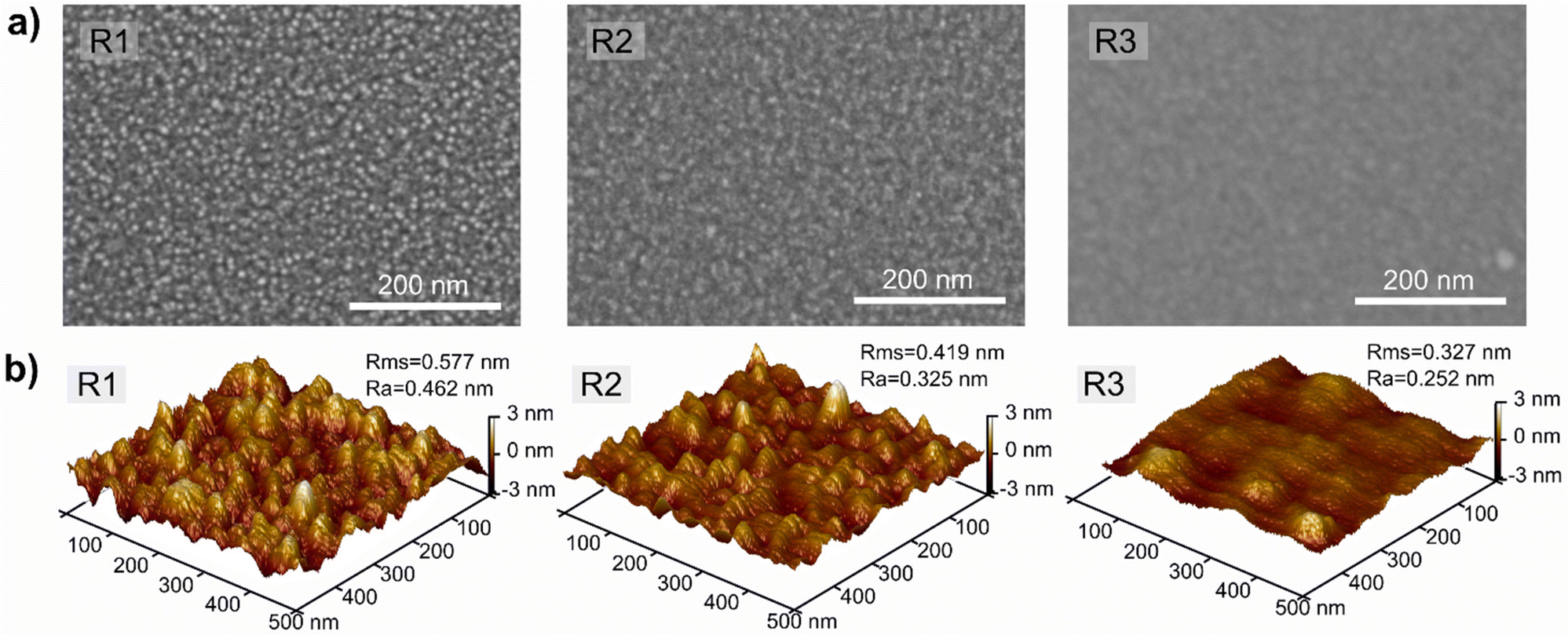 | ||
| Fig. 5 (a) Top-view SEM images showing the surface morphology of nanolaminate ZnO/Al2O3 film from different regions R1, R2, and R3. (b) AFM images displaying the surface roughness over 500 × 500 nm2 areas of the same regions. Both RMS and Ra roughness values are included. | ||
Following the observed morphological changes in SEM results, a topographic AFM characterization was performed to obtain quantitative roughness information. The nanolaminate sample presented more defined vertically aligned nanostructures in R1, and a progressively smoother surface was observed in R2 and R3 as the thickness of the Al2O3 layer increased. The roughness information for R1, R2, and R3 was obtained by AFM from 500 nm × 500 nm area scan and is plotted in Fig. 5b. The distinct vertical ZnO grains, which are clearly discernible in R1, become gradually broader in R2 and R3. From these measurements, the arithmetic average (Ra) and root mean square (RMS) of the profile height variations were derived, yielding RMS [Ra] values of 0.577 [0.462] nm, 0.419 [0.325] nm, and 0.327 [0.252] nm for R1, R2, and R3, respectively, which indicate a gradual decrease in surface roughness.
GI-XRD analysis was employed to elucidate the crystallinity of the films. Gaussian fitting of the (002) peaks yielded full widths at half maximum of 0.62°, 1.49°, and 1.42° for R1, R2, and R3, respectively. Furthermore, a subtle yet distinct sharp Si (311) reflection was observed at 56.2° in R2 and R3, as denoted by an asterisk in Fig. 6. The calculated penetration depth at a 0.34° incidence angle revealed a significant disparity between the ZnO and Al2O3 materials due to their differing absorption coefficients; specifically, the penetration depths were determined to be 57.47 nm for ZnO and 263.84 nm for Al2O3, as illustrated in Fig. S1.†
 | ||
| Fig. 6 GI-XRD patterns of the thin film sample at incident angles of 0.34°. The diffraction peaks correspond to the crystalline phases present in the surface layer, with a notable decrease in the (002) peak of ZnO by increasing Al2O3 composition, indicating a reduction of crystalline quality. PDF Card – 04-020-0364 used as a reference ZnO spectra the intensity multiplied fifty times. | ||
TEM analysis provides a distinct formation of multilayers in regions R2 and R3. Fig. 7a shows cross-sectional images of ZnO/Al2O3 nanolaminate films with varying Al2O3 layer thicknesses in both regions. A detailed image analysis was conducted to measure the layer thicknesses: in R2, the average ZnO and Al2O3 layer thicknesses were determined to be 5.03 nm and 3.31 nm, respectively. In contrast, in R3, the corresponding values were 5.51 nm and 5.12 nm, with a measurement deviation of approximately 0.3 nm in both regions. Additionally, in both regions, the first ZnO layer is slightly thicker (∼6 nm) compared to subsequent ZnO layers, which are consistently 5 nm. The Al2O3 layer thickness is controlled at 3 nm in R2 and 5 nm in R3. High-resolution TEM images in Fig. 7b reveal that ZnO exhibits a polycrystalline nature with distinct lattice parameters, whereas Al2O3 forms an amorphous structure. Within the ZnO layers, apparent grain boundary defects are observed, with ZnO grain size limited to 5 nm due to interruption by the Al2O3 layers. Furthermore, while no diffusion from the Al2O3 layer into the well-crystalline ZnO grains is observed, diffusion at the grain boundaries is evident. The lattice distance of the (002) planes is slightly higher than the unstressed ZnO lattice distance (2.6 Å), and the (002) plane orientations appear random, aligning with the XRD results for both R2 and R3.
 | ||
| Fig. 7 TEM analysis of ZnO/Al2O3 nanolaminate films. (a) TEM cross-sectional image shows the ZnO/Al2O3 bilayer deposited with eight super-cycle. ZnO and Al2O3 sublayers have been annotated (b) HR-TEM image showing lattice fringes with a measured spacing of 2.7 Å for ZnO film. (c) SAED pattern indexed to the ZnO (PDF Card – 04-020-0364). | ||
In Fig. 7c, the SAED pattern of the ZnO/Al2O3 film is presented; the Debye–Scherrer rings comprise a combination of rings and spots that indicate the polycrystalline nature of ZnO, and region R3 exhibits slightly more intense spots, which might be attributable to larger ZnO grains in the local SAED characterization zone. The SAED pattern matches well with the ZnO reference (PDF Card – 04-020-0364), and the indexed diffraction patterns indicate stronger reflections from the (100), (002), and (101) planes. In general, the TEM and SAED results collectively demonstrate the properties of well-crystalline ZnO and amorphous Al2O3 layers, and the cross-sectional images illustrate highly reproducible layer thicknesses and sharp interfaces along the multilayer structure, thereby highlighting the consistency of super-cycle deposition with multi-head SALD even in open-air conditions.
Surface potential properties
In ZnO/Al2O3 nanolaminate films, changing the sublayer thickness enables the tuning of the work function of the film.11 Fig. 8 demonstrates the variations in the work function with increasing Al2O3 thickness using a Kelvin probe setup, where the work function values are plotted as a function of measurement location in our gradient film. The Kelvin probe presented a surface potential of 197.55 ± 8.92 mV on a gold (Au) reference sample, which is an expected value.59 The calculated work functions (φ) relative to the Au reference (φAu = 5.1 eV) are presented on the right y-axis. The first three data points (0–15 mm) are relatively high contact potential difference (VCPD) values (–147.6 ± 2.1 mV), corresponding to an average work function of 4.75 ± 0.02 eV. The initial points likely represent regions where the Al2O3 coverage is still minimal; in these regions, the surface is dominated by ZnO or is partially covered by Al2O3. The slight variation in these values may be attributed to local doping changes or the initial onset of Al2O3 coverage. Between 15–25 mm, a sharp decrease in surface potential to −546.8 ± 2.3 mV (φ = 4.35 eV) is observed. This change likely indicates that sufficient Al2O3 is present to alter the near-surface electronic structure, for instance, through band bending in ZnO, passivation of surface states, or screening by the Al2O3.60 Above 35 mm, after reaching a threshold coverage of Al2O3, the measured work function begins to recover gradually toward positive values up to a value of −448.0 ± 2.6 mV resulting in φ = 4.46 eV. | ||
| Fig. 8 The contact potential difference, represented on the left y-axis, and the calculated work function values, displayed on the right y-axis, were systematically measured at various points on the investigated samples. | ||
Discussion
Spatial film thickness variation and mass transport dynamics
When GPC values were calculated using ellipsometry for nanolaminates and compared with those of reference ZnO and Al2O3 films, the ZnO thickness matched expectations. The Al2O3 thickness, however, showed discrepancies. The Al2O3 films in the nanolaminate had a GPC of 0.187 nm, as opposed to 1.55 nm per cycle for individual Al2O3 films. Consequently, rather than attributing these differences to variations in the ZnO layer thickness, it is plausible that the change arises from the utilization of a four-wave ellipsometry model that was not specifically designed for alternating ZnO and Al2O3 layers; the differing refractive indices for each layer may have introduced discrepancies when measuring the bulk nanolaminate thickness. For more precise bulk thickness measurements in nanolaminates, it is recommended that spectroscopic ellipsometry (SE) or X-ray reflectivity (XRR) techniques, combined with rigorous modeling and fitting procedures, be employed as corroborated by other studies.61 Furthermore, TEM results indicated that the initial ZnO layer was slightly thicker (by less than 1 nm) compared to subsequent ZnO layers. Although this observation might initially be interpreted as a difference in GPC of ZnO on the native SiO2 layer, it should be noted that at the start of the deposition process the substrate passed under the injection head when returning to the starting position. Thereby undergoing an extra ALD cycle that resulted in a marginally thicker initial ZnO layer. An alternative perspective considers the conversion-etch effect of the TMA precursor on the ZnO film, a phenomenon previously reported by Zywotko et al.62 for atomic layer etching (ALE) of ZnO. This may also explain the observed differences in Al2O3 GPC for individual (0.187 nm) and bulk nanolaminate (0.155 nm). Nevertheless, the remainder of the layers exhibited reproducible thickness with sharply defined interfaces, a characteristic attributed to the inherent nature of the ALD mechanism. Notably, although previous trials with mono-head SALD have been conducted,41,63 achieving interfaces of such sharpness under open-air conditions has not been previously reported. In the present study, the application of SALD under open-air conditions via a super-cycle approach has yielded interfaces of exceptional sharpness.Additionally, our CFD simulations underscore a strong correlation between film thickness and the amount of TMA molecule transported for a particular head design. The initial 15–30 mm region appears to exhibit a sharp increase in TMA mass transport, as indicated by the concentration, velocity, and pressure results in Fig. 4b. This behavior strongly correlates with the final film thickness gradient, which manifests as a smooth, step-like transition rather than a linear one. Furthermore, achieving a more controlled thickness gradient necessitates a comprehensive understanding of the interplay between combinatorial head geometry, deposition parameters, and precursor chemistry, which would constitute a significant advancement in the design of more efficient deposition heads for combinatorial film depositions using SALD. Such an investigation may require the development of a mathematical model supported by multiphysics simulations and experimental data, which is beyond the primary focus of the present article.
Structural and morphological properties
In addition, ZnO demonstrates high crystallinity and strong c-axis orientation on a native silicon oxide layer even at a 40 nm thickness. However, an increase in the thickness of the amorphous Al2O3 layer diminishes the bulk crystalline properties of the nanolaminate, as evidenced by a ZnO (002) diffraction peak that remains apparent but becomes weaker and broader. When the FWHM of the diffraction peaks are calculated, a substantial difference is observed between region R1 and the other regions, whereas the difference between regions R2 and R3 is minimal. This phenomenon can be attributed to the interruption of ZnO growth by each 5 nm increment of the amorphous Al2O3 layer, which confines the ZnO crystallite size and results in broader diffraction peaks; however, further increases in Al2O3 thickness do not contribute additional broadness to the nanolaminate film. The results further indicate that the crystallinity of the ZnO/Al2O3 system is directly related to the number of ZnO ALD cycles, thereby permitting tunability in crystallinity. Moreover, TEM results (Fig. 7) also indicate that an increased amorphous Al2O3 layer does not affect the crystallinity of the individual ZnO layers. Notably, silicon peaks appear exclusively in regions R2 and R3, which is attributed to the increased penetration depth of the Al2O3 layer; calculated values in Fig. S1† show a significant disparity in penetration depths between ZnO (57 nm) and Al2O3 (264 nm) under identical X-ray incidence conditions, a factor that may contribute to the detection of increased silicon reflection intensities. In contrast, in region R1, the lower ZnO penetration depth may lead to only a minor contribution to the (2![[1 with combining macron]](https://www.rsc.org/images/entities/char_0031_0304.gif) 0) ZnO reflection, a contribution that remains indistinguishable at the resolution of current X-ray diffraction measurements, which results as a broader peak including both ZnO and Si components.
0) ZnO reflection, a contribution that remains indistinguishable at the resolution of current X-ray diffraction measurements, which results as a broader peak including both ZnO and Si components.
Based on SEM and AFM results, the thickness of the Al2O3 layer provides considerable tunability in controlling surface roughness. Given that the preferentially c-axis oriented ZnO (R1) exhibits high roughness even at a thickness of 40 nm, lamination with Al2O3 (R2 and R3) effectively reduces surface protrusions and smooths the film. These smoother surfaces decrease photon scattering, thereby resulting in higher transmittance and lower absorbance,64 which may be advantageous for applications that require highly uniform thin films, such as transparent conducting electrodes or heterostructures for electronic devices. In contrast, rougher surfaces scatter and trap more photons, which increases the likelihood of photon absorption and the generation of electron–hole pairs that facilitate the photocatalytic process.65 Additionally, rough surfaces provide more active sites, which improves the molecular adhesion of the photocatalytic adsorbates, it is important to note that excessively rough surfaces can cause coarsening of adsorbates, thereby reducing adsorption efficiency,65 which suggests that optimization of surface roughness is crucial. Therefore, by employing a multi-head SALD system to tailor the Al2O3 sublayer thickness, one can fine-tune surface roughness to balance high optical transmittance with enhanced photocatalytic activity, thereby optimizing thin film performance across diverse applications.
Surface chemistry and work function
Different from XPS, the EDS analysis revealed a small amount of Al content (0.58 at%), and it has been previously noted that surface roughness plays an important role in the error rates in EDS.66 The roughest morphology observed in R1 might lead to increased error rates due to the EDS scattering mechanism. However, it has been clearly observed that the chemical composition ratio of Al increases with increasing Al2O3 layer thickness, although the Zn content does not exhibit the same atomic percentage. In EDS, the absorption mechanism of nanolaminates with varying thickness greatly alters the measured chemical composition, as demonstrated by the PRZ distribution obtained from MC simulation (Fig. S2†), which shows that increased nanolaminate thickness significantly impacts the total X-ray absorption of Si, while Zn maintains consistent absorption values across all regions. This effect is attributed to the increased bulk nanolaminate thickness in R2 and R3, where the penetration depth gradually decreases, thereby reducing Si information and resulting in an overall increased signal for the other elements; thus, XPS results may be more convenient for quantitative analysis when only shallow information depth is required.In XPS results, the Zn intensity gradually decreases with increasing Al2O3 due to attenuation by the upper Al2O3 layer (Fig. 3b and Fig. 7a). In R2 and R3, the Al2p binding energies exhibit slight shifts that are attributed to the higher Al2O3 content. As an insulating material, Al2O3 causes the applied flood gun conditions to be insufficient in fully compensating for surface charging during sequential HR-XPS spectrum acquisition, leading to differential shifts in the adventitious carbon peak relative to other elements in the same sample.67 In contrast to the EDS results, the HRXPS results show no trace of Al contribution in R1. Furthermore, the gradual increase of Al content in R2 and R3 proves the reliability of the SALD method for precise chemical composition control and the avoidance of unwanted mixing. The O1s peak in R2 and R3 presents a different shape and intensity compared to R1, which is due to the increased Al2O3 layer thickness contributing significantly to the Al2O3 lattice oxygen (O4); furthermore, in the O1s spectra of R2 and R3, the binding energies corresponding to ZnO–H2O and Zn–OH bonds have disappeared owing to the new top layer of Al2O3. In the XPS results, R1 shows the highest C1s atomic percentage (Table S1†) compared to R2 and R3, a phenomenon that can be attributed to the surface roughness since rougher surfaces have a larger effective surface area available for the adsorption of hydrocarbons and carbonaceous contaminants.68 A relatively higher O atomic percentage could be due to water and hydroxyls adsorbed on the surface, which often introduce extra oxygen signals; when the surface roughness decreases in R2 and R3, the stoichiometry improves, although the ratios remain O-rich.
Film stoichiometry is a critical factor in open-air deposition methods. Previous studies have reported that open-air deposition techniques can incorporate more oxygen into deposited films compared to vacuum-based methods due to the presence of atmospheric oxygen in the deposition environment.69 Nyugen et al. demonstrated the impact of open-air SALD on the carrier mobility of Al-doped ZnO films. Typically, stoichiometric calculations involve sputtering the surface carbon layer with argon gas. However, due to the presence of a thin 3 nm Al2O3 top layer, Ar sputtering is avoided to prevent potential damage to this layer. Instead, the model proposed by Henderson et al.51 has been employed to carefully account for the contribution of carbon species and extract calculated stoichiometric information. As shown in Table S2,† the Zn:O ratio at the surface is approximately 1:1, indicating high phase purity and stable material composition. Furthermore, despite being an open-air deposition method, our study determined that the overall metal-to-oxide ratio closely aligns with the expected stoichiometric values across all examined regions (Table S2†).
The variations in surface potential correlated to the varying composition of the investigated surfaces. The hydroxylated intrinsic ZnO surface attributes the initial high values. This yields a higher VCPD compared to the reference Au sample, which is consistent with previous reports.70 This suggests that local doping variations are minimal and that the Al2O3 coverage is slight. As a highly surface-sensitive method, the Kelvin probe method focuses on the outermost atomic layers about 3 nm.71 With partial Al2O3 coverage on the ZnO surface, the measured VCPD and φ progressively shift to lower values. This is in agreement with the characteristic of Al and Al2O3.72 It also relates to a potential barrier forming at the interface between the sub-layers. Al2O3 is well known to passivate surface states on ZnO and other semiconductors, thereby modifying the Fermi-level position at or near the surface.73 A thin layer of Al2O3 helps cover the ZnO surface. This reduces the dangling bonds and lowers defect-induced Fermi-level pinning. As a result, the surface potential is minimized. Schuldis et al.74 demonstrated that a 0.5 nm-thick Al2O3 layer provides optimal surface passivation. Our findings support this claim, the region where a thin Al2O3 layer leads to a significant accumulation of charges at the ZnO/Al2O3 interface. As the Al2O3 layer gets thicker, the insulating surface potential weakens the net effect, which raises the work function. Sufficient Al2O3 coverage can enhance the electron affinity effect and reduce the measured work function. Thin ZnO layers (under 1 nm) can show the Maxwell–Wagner polarization effect. However, the 5 nm ZnO thickness in this study does not present such significant charge buildup from this effect.9
Conclusion
The important contribution of this study is the demonstration of a novel approach to control the usage of multiple precursors in an open-air SALD method, which allows for exceptional dosing control. This multi-head system permits the use of optimized head designs and pulse times (substrate speed) for each material deposition, a feature that is not feasible with conventional mono-head SALD systems operating in a super-cycle approach. Furthermore, the multi-head setup allows the implementation of different custom head designs. In the present study, a combinatorial head was employed to demonstrate the impact of Al2O3 sublayer thickness on ZnO/Al2O3 nanolaminate films. The use of separated heads prevents issues such as premature surface saturation and competition between different precursors, resulting in more stable growth kinetics and improved stoichiometric control. Consequently, the multi-head SALD method yielded no evidence of unwanted aluminum contamination in regions where TMA was not injected. Cross-sectional TEM images confirmed that the nanolaminate film exhibited high reproducibility in each sublayer and well-defined, sharp interfaces. Furthermore, XPS results revealed no trace of alloying and a favorable elemental ratio, thereby affirming that the key merits of ALD can be realized in open-air using the demonstrated approach. Finally, work function analyses confirm that partial Al2O3 coverage passivates ZnO surfaces, leading to controlled electronic properties, underscoring the promise of SALD for functional thin-film fabrication in a precise manner.While the paper presents comprehensive results on combinatorial ZnO/Al2O3 nanolaminates, the multi-head SALD technique shows promising potential for controlled doping and optimization of various multi-material depositions. Precise control of this super-cycle approach, coupled with the incorporation of machine learning into the combinatorial SALD approach, holds significant potential as a rapid and effective technique for experimental studies in materials research. Moreover, combining this multi-head method with surface treatments, such as plasma, ozone, or UV, and in situ characterization techniques offers numerous opportunities for further advancements. These advanced approaches collectively establish SALD as an adaptable deposition method with broad potential for adoption in both scientific research and industrial applications.
Author contributions
H. O. undertook the conceptualization, combinatorial head design, material deposition, conducted data curation (with the exception of TEM and XPS), formal analysis, visualization and writing – original draft. M. I. B. conducted XPS formal analysis, validation and visualization. V. S. P. R. performed CFD data curation, and P. J. V. R. contributed to conceptualization and formal analysis of Kelvin probe. G. A. contributed to funding acquisition, while D. M. R. contributed to conceptualization and funding acquisition. All authors contributed to the review and editing of the manuscript.Conflicts of interest
The authors declare no competing financial interest.Data availability
The data supporting this article have been included as part of the ESI.†Acknowledgements
This work was supported by the Joint Plan Investissement d'Avenir (PIA) – LabEx MINOS. The authors also extend their sincere gratitude to Sonia Ortega Murillo (LMGP, Grenoble, France) and Laëtitia Rapenne (CMTC, Grenoble, France) for their invaluable contributions to XPS and TEM measurements, respectively.References
- U. Ozgur, et al., A comprehensive review of ZnO materials and devices, J. Appl. Phys., 2005, 98(4), 041301, DOI:10.1063/1.1992666.
- H. Okcu, G. Ardila, L. Rapenne, H. Roussel, C. Jiménez and D. Muñoz-Rojas, Open-Air deposition of Submicron Self-Textured ZnO thin films with high piezoelectric coefficients and oxygen polarity, Appl. Surf. Sci., 2025, 162945, DOI:10.1016/j.apsusc.2025.162945.
- E. Guziewicz, et al., Extremely low temperature growth of ZnO by atomic layer deposition, J. Appl. Phys., 2008, 103(3), 033515, DOI:10.1063/1.2836819.
- M. Willander, et al., Zinc oxide nanorod based photonic devices: recent progress in growth, light emitting diodes and lasers, Nanotechnology, 2009, 20(33), 332001, DOI:10.1088/0957-4484/20/33/332001.
- Y. Q. Wu, H. C. Lin, P. D. Ye and G. D. Wilk, Current transport and maximum dielectric strength of atomic-layer-deposited ultrathin Al2O3 on GaAs, Appl. Phys. Lett., 2007, 90(7), 072105, DOI:10.1063/1.2535528.
- V. Chawla, M. Ruoho, M. Weber, A. Chaaya, A. Taylor, C. Charmette, P. Miele, M. Bechelany, J. Michler and I. Utke, Fracture mechanics and oxygen gas barrier properties of Al2O3/ZnO nanolaminates on PET deposited by atomic layer deposition, Nanomaterials, 2019, 9(1), 88, DOI:10.3390/NANO9010088.
- T. Homola, et al., Mechanical properties of atomic layer deposited Al2O3/ZnO nanolaminates, Surf. Coat. Technol., 2015, 284, 198–205, DOI:10.1016/j.surfcoat.2015.07.078.
- C. F. Herrmann, F. DelRio, D. Miller, S. George, V. Bright, J. Ebel, R. Strawser, R. Cortez and K. Leedy, Alternative dielectric films for rf MEMS capacitive switches deposited using atomic layer deposited Al2O3/ZnO alloys, Sens. Actuators, A, 2007, 135(1), 262–272, DOI:10.1016/J.SNA.2006.07.002.
- M. Upadhyay, M. Ben Elbahri, M. Mezhoud, R. C. Germanicus and U. Lüders, Thickness dependence of dielectric properties in sub-nanometric Al2O3/ZnO laminates, Solid-State Electron., 2021, 186, 108070, DOI:10.1016/j.sse.2021.108070.
- J. Li, M. Liu and X. Bi, Interface electron polarization based high- k Al2 O3 /ZnO nanolaminates with excellent temperature stability and ultrahigh energy-storage density by atomic layer deposition, J. Mater. Chem. A, 2019, 7(17), 10303–10318, 10.1039/C9TA01487J.
- R. Viter, et al., Enhancement of Electronic and Optical Properties of ZnO/Al2 O3 Nanolaminate Coated Electrospun Nanofibers, J. Phys. Chem. C, 2016, 120(9), 5124–5132, DOI:10.1021/acs.jpcc.5b12263.
- J. López, et al., Refractive index and bandgap variation in Al2O3-ZnO ultrathin multilayers prepared by atomic layer deposition, J. Alloys Compd., 2017, 691, 308–315, DOI:10.1016/j.jallcom.2016.08.271.
- J. López, et al., Thickness effect on the optical and morphological properties in Al2O3/ZnO nanolaminate thin films prepared by atomic layer deposition, Superlattices Microstruct., 2016, 90, 265–273, DOI:10.1016/j.spmi.2015.12.022.
- Q. Yu, et al., Highly sensitive strain sensors based on piezotronic tunneling junction, Nat. Commun., 2022, 13(1), 778, DOI:10.1038/s41467-022-28443-0.
- A. A. Chaaya, et al., Tuning Optical Properties of Al2 O3 /ZnO Nanolaminates Synthesized by Atomic Layer Deposition, J. Phys. Chem. C, 2014, 118(7), 3811–3819, DOI:10.1021/jp411970w.
- F. Romo-Garcia, et al., Optoelectronic attenuation behavior of Al2O3/ZnO nanolaminates grown by Atomic Layer Deposition, Thin Solid Films, 2019, 669, 419–424, DOI:10.1016/j.tsf.2018.11.026.
- J.-H. Lee, et al., Enhancing the thermoelectric properties of super-lattice Al2O3/ZnO atomic film via interface confinement, Ceram. Int., 2016, 42(13), 14411–14415, DOI:10.1016/j.ceramint.2016.06.032.
- M. Polat Gonullu, Design and characterization of single bilayer ZnO/Al2O3 film by ultrasonically spray pyrolysis and its application in photocatalysis, Micro Nanostruct., 2022, 164, 107113, DOI:10.1016/j.spmi.2021.107113.
- R. Singh, H. Shin, S. Nah, J.-Y. Park and H. Seo, Femto-second and nanoscale hot carrier dynamics in ZnO/Al2O3/Ag-NWs/FTO heterojunction, J. Alloys Compd., 2021, 872, 159657, DOI:10.1016/j.jallcom.2021.159657.
- A. A. Chaaya, Design of oxide based nanomaterials by ALD: from sensors to membrane application, 2017.
- H. Kim, Z. Wang, M. Hedhili, N. Wehbe and H. Alshareef, Oxidant-dependent thermoelectric properties of undoped ZnO films by atomic layer deposition, 2017, DOI:10.1021/ACS.CHEMMATER.6B04654.
- D. Muñoz-Rojas, T. Maindron, A. Esteve, F. Piallat, J. C. S. Kools and J.-M. Decams, Speeding up the unique assets of atomic layer deposition, Mater. Today Chem., 2019, 12, 96–120, DOI:10.1016/j.mtchem.2018.11.013.
- D. Muñoz-Rojas, V. H. Nguyen, C. Masse de la Huerta, S. Aghazadehchors, C. Jiménez and D. Bellet, Spatial Atomic Layer Deposition (SALD), an emerging tool for energy materials. Application to new-generation photovoltaic devices and transparent conductive materials, C. R. Phys., 2017, 18(7), 391–400, DOI:10.1016/j.crhy.2017.09.004.
- P. Poodt, et al., Spatial atomic layer deposition: A route towards further industrialization of atomic layer deposition, J. Vac. Sci. Technol., 2012, 30(1), 010802, DOI:10.1116/1.3670745.
- H. K. Park, B. S. Yang, S.-H. Park, M. S. Kim, J. C. Shin and J. Heo, Purge-time-dependent growth of ZnO thin films by atomic layer deposition, J. Alloys Compd., 2014, 605, 124–130, DOI:10.1016/J.JALLCOM.2014.03.169.
- J. P. Vale, et al., Can We Rationally Design and Operate Spatial Atomic Layer Deposition Systems for Steering the Growth Regime of Thin Films?, J. Phys. Chem. C, 2023, 127(19), 9425–9436, DOI:10.1021/acs.jpcc.3c02262.
- M. F. K. Niazi, D. Muñoz-Rojas, D. Evrard and M. Weber, Comparative Study of the Environmental Impact of Depositing Al2O3 by Atomic Layer Deposition and Spatial Atomic Layer Deposition, ACS Sustainable Chem. Eng., 2023, 11, 15072–15082, DOI:10.1021/acssuschemeng.3c04135.
- M. Weber, et al., Assessing the Environmental Impact of Atomic Layer Deposition (ALD) Processes and Pathways to Lower It, ACS Mater. Au, 2023, 3(4), 274–298, DOI:10.1021/acsmaterialsau.3c00002.
- C. Masse de la Huerta, V. H. Nguyen, J.-M. Dedulle, D. Bellet, C. Jiménez and D. Muñoz-Rojas, Influence of the Geometric Parameters on the Deposition Mode in Spatial Atomic Layer Deposition: A Novel Approach to Area-Selective Deposition, Coatings, 2019, 9(1), 1, DOI:10.3390/coatings9010005.
- T. T. Nguyen, D. Nguyen Thi Kieu, H. V. Bui, L. Le Thi Ngoc and V. H. Nguyen, Enhancing control in spatial atomic layer deposition: Insights into precursor diffusion, geometric parameters, and CVD mitigation strategies, Nanotechnology, 2024, 35(20), 205601, DOI:10.1088/1361-6528/ad28d6.
- Y. C. Jung, et al., A Novel Combinatorial Approach to the Ferroelectric Properties in HfZr1–O2 Deposited by Atomic Layer Deposition, Phys. Status Solidi RRL, 2021, 15(5), 2100053, DOI:10.1002/pssr.202100053.
- H. S. Kim, et al., Realization of Spatially Addressable Library by a Novel Combinatorial Approach on Atomic Layer Deposition: A Case Study of Zinc Oxide, ACS Comb. Sci., 2019, 21(6), 445–455, DOI:10.1021/acscombsci.9b00007.
- A. H. Alshehri, et al., Nanoscale film thickness gradients printed in open air by spatially varying chemical vapor deposition, Adv. Funct. Mater., 2021, 31, 2103271, DOI:10.1002/adfm.202103271.
- Z. Gao and P. Banerjee, Review Article: Atomic layer deposition of doped ZnO films, J. Vac. Sci. Technol., A, 2019, 37(5), 050802, DOI:10.1116/1.5112777.
- B. Macco, et al., Temporal and spatial atomic layer deposition of Al-doped zinc oxide as a passivating conductive contact for silicon solar cells, Sol. Energy Mater. Sol. Cells, 2022, 245, 111869, DOI:10.1016/j.solmat.2022.111869.
- D. Lancaster, H. Sun and S. George, Atomic layer deposition of Zn(O,S) alloys using diethylzinc with H2O and H2S: Effect of exchange reactions, J. Phys. Chem. C, 2017, 121, 34, DOI:10.1021/ACS.JPCC.7B05361.
- A. Mohammad, S. Ilhom, D. Shukla and N. Biyikli, In situ monitoring atomic layer doping processes for Al-doped ZnO layers: Competitive nature of surface reactions between metal precursors, J. Vac. Sci. Technol., A, 2022, 40(4), 042401, DOI:10.1116/6.0001772.
- B. Macco and W. M. M. Kessels, Atomic layer deposition of conductive and semiconductive oxides, Appl. Phys. Rev., 2022, 9(4), 041313, DOI:10.1063/5.0116732.
- H. Wang, et al., Rapid thermal processing induced interfacial diffusion and solid reaction in the Al2O3/ZnO nano-laminates films, Ceram. Int., 2024, 50(23), 51858–51862, DOI:10.1016/j.ceramint.2024.02.223.
- G. B. Lee, S. H. Song, M. W. Lee, Y. J. Kim and B. H. Choi, Characterization of physical and mechanical properties of Al2O3-doped ZnO (AZO) thin films deposited on transparent polyimide supports with various ALD process parameters, Appl. Surf. Sci., 2021, 535, 147731, DOI:10.1016/J.APSUSC.2020.147731.
- H. Asgarimoghaddam, S. S. Khamgaonkar, A. Mathur, V. Maheshwari and K. P. Musselman, Enhancing Internal and External Stability of Perovskite Solar Cells Through Polystyrene Modification of the Perovskite and Rapid Open–Air Deposition of ZnO/AlO x Nanolaminate Encapsulation, Sol. RRL, 2024, 8(14), 2400111, DOI:10.1002/solr.202400111.
- B. D. Cullity and S. R. Stock, Elements of X-ray diffraction, Pearson Education, Harlow, 3. ed. new Internat. edn, 2014 Search PubMed.
- N. Fairley, et al., Systematic and collaborative approach to problem solving using X-ray photoelectron spectroscopy, Appl. Surf. Sci. Adv., 2021, 5, 100112, DOI:10.1016/j.apsadv.2021.100112.
- C. A. Schneider, W. S. Rasband and K. W. Eliceiri, NIH Image to ImageJ: 25 years of image analysis, Nat. Methods, 2012, 9(7), 671–675, DOI:10.1038/nmeth.2089.
- Origin(Pro), Northampton, MA, USA, 2025 Search PubMed.
- M. Wojdyr, Fityk: a general-purpose peak fitting program, J. Appl. Crystallogr., 2010, 43(5), 1126–1128, DOI:10.1107/S0021889810030499.
- S. Seddio, An Improved Sum Peak Removal Method for EDS Analysis, Microsc. Microanal., 2024, 30(Supplement_1), ozae044.095, DOI:10.1093/mam/ozae044.095.
- L. H. Grey, H.-Y. Nie and M. C. Biesinger, Defining the nature of adventitious carbon and improving its merit as a charge correction reference for XPS, Appl. Surf. Sci., 2024, 653, 159319, DOI:10.1016/j.apsusc.2024.159319.
- D. Barreca, A. Gasparotto, C. Maccato, C. Maragno and E. Tondello, ZnO Nanoplatelets Obtained by Chemical Vapor Deposition, Studied by XPS, Surf. Sci. Spectra, 2009, 14(1), 19–26, DOI:10.1116/11.20071001.
- L. Sygellou, et al., ZrO2 and Al2O3 Thin Films on Ge(100) Grown by ALD: An XPS Investigation, Surf. Sci. Spectra, 2012, 18(1), 58–67, DOI:10.1116/11.20100901.
- J. D. Henderson, B. P. Payne, N. S. McIntyre and M. C. Biesinger, Enhancing Oxygen Spectra Interpretation by Calculating Oxygen Linked to Adventitious Carbon, Surf. Interface Anal., 2025, 57(3), 214–220, DOI:10.1002/sia.7376.
- T. J. Frankcombe and Y. Liu, Interpretation of Oxygen 1s X-ray Photoelectron Spectroscopy of ZnO, Chem. Mater., 2023, 35(14), 5468–5474, DOI:10.1021/acs.chemmater.3c00801.
- A. H. Alshehri, et al., Quantum-tunneling metal-insulator-metal diodes made by rapid atmospheric pressure chemical vapor deposition, Adv. Funct. Mater., 2019, 29(7), 1805533, DOI:10.1002/adfm.201805533.
- D. H. Levy, S. F. Nelson and D. C. Freeman, Oxide Electronics by Spatial Atomic Layer Deposition, IEEEOSA J. Disp. Technol., 2009, 5(12), 484–494, DOI:10.1109/jdt.2009.2022770.
- A. Illiberi, R. Scherpenborg, Y. Wu, F. Roozeboom and P. Poodt, Spatial atmospheric atomic layer deposition of AlxZn1-xO., ACS Appl. Mater. Interfaces, 2013, 5(24), 13124–13128, DOI:10.1021/am404137e.
- L. Hoffmann, et al., Gas diffusion barriers prepared by spatial atmospheric pressure plasma enhanced ALD, ACS Appl. Mater. Interfaces, 2017, 9(4), 4171–4176, DOI:10.1021/acsami.6b13380.
- C. R. Ellinger and S. F. Nelson, Selective area spatial atomic layer deposition of ZnO, al 2 O 3, and aluminum-doped ZnO using poly(vinyl pyrrolidone), Chem. Mater., 2014, 26(4), 1514–1522, DOI:10.1021/cm402464z.
- C.-H. Chao, P.-W. Chi and D.-H. Wei, Investigations on the Crystallographic Orientation Induced Surface Morphology Evolution of ZnO Thin Films and Their Wettability and Conductivity, J. Phys. Chem. C, 2016, 120(15), 8210–8219, DOI:10.1021/acs.jpcc.6b01573.
- P. A. Anderson, Work Function of Gold, Phys. Rev., 1959, 115(3), 553–554, DOI:10.1103/PhysRev.115.553.
- C. Chen, H. He, Y. Lu, K. Wu and Z. Ye, Surface Passivation Effect on the Photoluminescence of ZnO Nanorods, ACS Appl. Mater. Interfaces, 2013, 5(13), 6354–6359, DOI:10.1021/am401418b.
- J. M. Jensen, A. B. Oelkers, R. Toivola, D. C. Johnson, J. W. Elam and S. M. George, X-ray Reflectivity Characterization of ZnO/Al2 O3 Multilayers Prepared by Atomic Layer Deposition, Chem. Mater., 2002, 14(5), 2276–2282, DOI:10.1021/cm011587z.
- D. R. Zywotko and S. M. George, Thermal Atomic Layer Etching of ZnO by a ‘Conversion-Etch’ Mechanism Using Sequential Exposures of Hydrogen Fluoride and Trimethylaluminum, Chem. Mater., 2017, 29(3), 1183–1191, DOI:10.1021/acs.chemmater.6b04529.
- R. Chen, et al., Spatial atomic layer deposition of ZnO/TiO2 nanolaminates, J. Vac. Sci. Technol., A, 2016, 34(5), 051502, DOI:10.1116/1.4955289.
- C.-L. Fern, et al., Surface Roughness-Induced Changes in Important Physical Features of CoFeSm Thin Films on Glass Substrates during Annealing, Materials, 2023, 16(21), 21, DOI:10.3390/ma16216989.
- F. Tulli, J. M. N. Morales, E. E. Salas, F. E. Morán Vieyra and C. D. Borsarelli, Photocatalytic Efficiency Tuning by the Surface Roughness of TiO2 Coatings on Glass Prepared by the Doctor Blade Method, Photochem. Photobiol., 2021, 97(1), 22–31, DOI:10.1111/php.13320.
- Can I Trust My Quantitative EDS Data? | JEOL Resources. Accessed: Feb. 18, 2025. [Online]. Available: https://www.jeolusa.com/RESOURCES/Electron-Optics/Documents-Downloads/can-i-trust-my-quantitative-eds-data.
- B. Vincent Crist, XPS guide for insulators: Electron flood gun operation and optimization, surface charging, controlled charging, differential charging, useful FWHMs, problems and solutions, and advice, J. Vac. Sci. Technol., A, 2024, 42(3), 032803, DOI:10.1116/6.0003439.
- R. Köhler, D. Hellrung, D. Tasche and C. Gerhard, Quantification of Carbonic Contamination of Fused Silica Surfaces at Different Stages of Classical Optics Manufacturing, Materials, 2021, 14(7), 7, DOI:10.3390/ma14071620.
- V. H. Nguyen, et al., Atmospheric Plasma-Enhanced Spatial Chemical Vapor Deposition of SiO 2 Using Trivinylmethoxysilane and Oxygen Plasma, Chem. Mater., 2020, 32(12), 5153–5161, DOI:10.1021/acs.chemmater.0c01148.
- S. Kikuchi, Y. Takahashi and T. Sakata, Measurement on Work Function of Polycrystalline Zinc Oxide Covered by Organic Dye.
- P. Knotek, et al., Kelvin probe force microscopy of the nanoscale electrical surface potential barrier of metal/semiconductor interfaces in ambient atmosphere, Beilstein J. Nanotechnol., 2019, 10(1), 1401–1411, DOI:10.3762/bjnano.10.138.
- E.-G. Kim and J.-L. Brédas, The nature of the aluminum–aluminum oxide interface: A nanoscale picture of the interfacial structure and energy-level alignment, Org. Electron., 2013, 14(2), 569–574, DOI:10.1016/j.orgel.2012.11.028.
- V. Dhaka, et al., Protective capping and surface passivation of III-V nanowires by atomic layer deposition, AIP Adv., 2016, 6(1), 015016, DOI:10.1063/1.4941063.
- D. Schuldis, A. Richter, J. Benick, P. Saint-Cast, M. Hermle and S. W. Glunz, Properties of the c-Si/Al2O3 interface of ultrathin atomic layer deposited Al2O3 layers capped by SiNx for c-Si surface passivation, Appl. Phys. Lett., 2014, 105(23), 231601, DOI:10.1063/1.4903483.
Footnote |
| † Electronic supplementary information (ESI) available. See DOI: https://doi.org/10.1039/d5nr01812a |
| This journal is © The Royal Society of Chemistry 2025 |