
 Open Access Article
 This Open Access Article is licensed under a Creative Commons Attribution-Non Commercial 3.0 Unported Licence
Low temperature inkjet-printed metal oxide sensors for sensitive and selective NO2 detection†
P. K.
Shihabudeen
 a,
Shivam
Gupta
b,
Yu-Hsien
Lin
a,
Shih-Wen
Chiu
c,
Yu Ting
Chuang
d,
Yuan Fu
Tang
d,
Nyan-Hwa
Tai
b and
Kea-Tiong
Tang
*a
a,
Shivam
Gupta
b,
Yu-Hsien
Lin
a,
Shih-Wen
Chiu
c,
Yu Ting
Chuang
d,
Yuan Fu
Tang
d,
Nyan-Hwa
Tai
b and
Kea-Tiong
Tang
*a
aDepartment of Electrical Engineering, National Tsing Hua University, Taiwan. E-mail: kttang@ee.nthu.edu.tw
bDepartment of Materials Science and Engineering, National Tsing Hua University, Taiwan
cEnosim Bio-tech Co., Ltd, Hsinchu, Taiwan
dNational Applied Research Laboratories, Taiwan Semiconductor Research Institute, Taiwan
First published on 7th May 2025
Abstract
Advancements in gas sensor technology are critical for enhancing environmental monitoring and pollution control systems. Among the various sensor types, inkjet-printed gas sensors have emerged as a promising solution due to their low fabrication cost, scalable production, and compatibility with modern electronics. This study presents the development and characterization of inkjet-printed chemiresistive gas microsensors based on tin oxide (SnO2) and indium oxide (In2O3) for the detection of nitrogen dioxide (NO2), a major air pollutant associated with vehicular emissions and industrial activities. The sensors were fabricated on compact CMOS-compatible microchips, with integrated microheaters and electrodes measuring less than 250 × 250 μm, enabling miniaturization and potential on-chip integration for portable sensing platforms. Metal oxide sols were deposited using a precise inkjet printing technique, and crystallization of the sensing layers was achieved via localized heating through the integrated microheaters. The SnO2 sensor demonstrated excellent sensitivity at room temperature, detecting NO2 concentrations as low as 10 ppb, while the In2O3 sensor showed optimal performance at 100 °C with comparable detection limits. Both sensors exhibited linear response behavior over a range of NO2 concentrations, along with strong selectivity against common interfering gases. Although humidity induced minor fluctuations, both sensors maintained robust NO2 selectivity. These results underscore the potential of inkjet-printed metal oxide microsensors for developing compact, low-power, and highly sensitive gas detection systems.
Introduction
Environmental monitoring and pollution control are increasingly critical in the face of global environmental challenges. Accurate detection of nitrogen dioxide (NO2), a major pollutant, is essential for ensuring air quality and public health.1 Chemiresistive gas sensors are among the simplest and most effective devices for environmental monitoring, operating on the principle that the electrical resistance of a sensing material changes upon interaction with target gas molecules.2,3 Their straightforward design, ease of fabrication, and ability to provide real-time monitoring make them highly suitable for detecting various environmental pollutants including NO2. Furthermore, their compatibility with modern fabrication techniques allows for the development of advanced, low-cost sensor arrays and integrated systems, enhancing their versatility and practical application in air quality monitoring.4–9Semiconducting metal oxides (SMOs) are widely used in chemiresistive gas sensing due to their tunable properties. By engineering their shape and composition, SMOs can be optimized for enhanced sensing performance. Their excellent thermal stability and chemical inertness toward sensing gases help prevent long-term degradation, ensuring reliable operation. Among the most commonly employed SMOs for gas sensing are tin oxide (SnO2) and indium oxide (In2O3), both of which maintain stability and resist chemical reactions in the sensing environment. These oxides, in diverse forms, including nanoparticles, nanowires, and thin films, synthesized through methods such as sol–gel, hydrothermal, and spin coating techniques, find application in NO2 sensing.10–13
While these conventional fabrication methods are effective, they come with challenges such as long processing times, high temperatures, and material wastage, which hinder the development of scalable, cost-efficient sensors.14,15 These drawbacks highlight the need for alternative fabrication techniques that offer better control and efficiency in gas sensor development. Inkjet printing is a scalable, mask-free fabrication technique that enables the precise deposition of functional materials with minimal material waste. Compared to conventional methods such as sol–gel processing, hydrothermal synthesis, and spin-coating, inkjet printing offers advantages including low-cost batch fabrication, direct patterning on flexible or CMOS-compatible substrates, and reduced process complexity. These features make it a promising technique for microsensor fabrication and integration into smart sensing platforms. Moreover, inkjet printing offers a clean, efficient, and highly adaptable method.16,17 Utilizing cartridges with micrometer-sized holes, this method ensures precision printing with droplet sizes in the picolitre range.17–19 Its versatility enables the printing of a wide range of materials, including metal oxide sols, nanoparticle suspensions, polymers, and more, making it ideal for application in biosensors, supercapacitors, solar cells, and various other advanced technologies.20–22
In recent years, inkjet-printed gas sensors have gained considerable attention due to their potential to significantly reduce production costs and simplify the fabrication process. This technique enables the direct deposition of metal oxide inks onto a variety of substrates at room temperature, offering a scalable and versatile approach. As a result, inkjet-printed gas sensors are emerging as a promising technology for revolutionizing real-time air quality monitoring. However, most studies have focused on polymer-based and graphene-based sensors, which operate at room temperature but exhibit limited sensitivity to NO2.23–25 Devabharathi et al. explored inkjet-printed SnO2 sol-based NO2 sensors, which required post-print annealing to enhance their structural and electrical properties.18 Their research demonstrated that inkjet printing could produce uniform mesoporous SnO2 films with good sensitivity to NO2, with the mesoporous structure playing a key role in improving gas adsorption and sensor performance. However, a significant drawback of this approach is the relatively high operating temperature required, which limits the practical application of these sensors in ambient or room-temperature environments. In contrast, Ogbeide et al. developed a room-temperature NO2 sensor using a composite of reduced graphene oxide (rGO) and copper cobalt oxide (CuCoOx), eliminating the need for post-print annealing.26 The use of a composite suspension ink allowed for a more straightforward fabrication process and enhanced the sensor's performance at ambient temperatures. However, while the sensor exhibited improved ease of fabrication, it still showed a lower response to NO2 and was prone to cross-sensitivity to ammonia, a common issue in gas sensors that detect multiple compounds. These limitations suggest that while the room-temperature operation is beneficial, it still requires optimization in terms of sensitivity and selectivity.
Moreover, most reported work on inkjet-printed gas sensors has focused on larger substrates, typically intended for broader environmental monitoring applications. The fabrication of inkjet-printed NO2 microsensors, which would allow for compact and portable devices with microchip integration, remains largely unexplored. In this work, we aim to address this gap by exploring the potential of inkjet printing for fabricating metal oxide microsensors on microchips with integrated microheaters. This approach combines the high sensitivity of metal oxide sensors with the precision and flexibility of inkjet printing, offering a promising route for efficient, real-time NO2 detection. We present two microsensors: a room-temperature SnO2-based sensor and a low-temperature In2O3-based sensor, both fabricated via inkjet printing using metal oxide sols. These sensors exhibit excellent sensitivity and selectivity at their respective optimal operating temperatures, paving the way for more efficient gas sensors.
Experimental
Preparation of ink
The metal oxide sol used as ink for inkjet printing was prepared using indium acetate (99.9% purity, Sigma-Aldrich), tin(II) 2-ethylhexanoate (99% purity, Sigma-Aldrich), and ethanolamine (99% purity, Sigma-Aldrich). The process began by dissolving 0.05 moles of indium acetate or tin(II) 2-ethylhexanoate in 40 mL of ethanol (99% purity, Sigma-Aldrich). Once fully dissolved, 3 mL of ethanolamine was gradually added dropwise as a stabilizing agent to ensure uniform precursor dispersion. The solution was continuously stirred at 60 °C for 4 hours, facilitating the reaction and forming a stable sol.To ensure reliable inkjet printing, the sol underwent a purification process. It was aged for seven days to enhance ink dispersion and stability. After aging, precipitates were removed to improve ink homogeneity. For further refinement, the sol was passed through a 0.22 μm membrane filter to eliminate any residual particulates. This filtration step was crucial for achieving high ink purity, preventing nozzle clogging, and enabling precise sensor fabrication.
Sensor fabrication
Fig. 1 illustrates the CMOS microchip and the various components and processes involved in fabricating the final sensor. Specifically, Fig. 1(a) shows the different layers of the CMOS substrate. The CMOS microheater is designed and fabricated using the TSMC 0.18 μm mixed-signal RF CMOS 1P6M process (one poly and six metals), in combination with the NARLabs TSRI (National Applied Research Laboratories, Taiwan Semiconductor Research Institute) backside silicon etch post-process. By etching the silicon backside, a cavity filled with air (which has a low thermal conductivity of 0.026 W (m K)−1) is created. This air-filled cavity acts as a thermal insulator, reducing heat conduction away from the heater.27 Consequently, the heater can achieve and maintain higher temperatures, which is crucial for precise thermal management and improves the overall energy efficiency and performance of the device. The heater's main structure features a parallel sandwich configuration consisting of metal 4 (AlCu), via 4 bar (tungsten), and metal 5 (AlCu). The interdigitated electrode (IDE) is constructed using metal 6, which is the top layer on the chip with a thickness of 2 μm, for temperature monitoring. | ||
| Fig. 1 (a) Various layers in the CMOS substrate, (b) the inkjet printing process, (c) the optical image of the substrate and (d) the final sensor assembly. | ||
Fig. 1(b) shows the DMP 2831 printer used in this study. The printer is equipped with a 16-head cartridge, each head featuring a 30 μm nozzle diameter and a print volume of 10 picolitres. In this research, a single head was employed to ensure precise deposition of the sensing material onto a 250 μm × 250 μm surface over the IDE. After printing, the material was dried at 60 °C for one hour to ensure optimal adhesion. The printing process was repeated twice to achieve uniform and comprehensive coverage. An optical image of the CMOS chips is shown in Fig. 1(c), and a cross-sectional diagram of the microchip is provided in Fig. S1.† Finally, the chip was wire-bonded onto a printed circuit board (PCB), forming the final sensor assembly as shown in Fig. 1(d).
Fig. 1(b) shows the DMP 2831 printer used in this study. The printer is equipped with a 16-head cartridge, each head featuring a 30 μm nozzle diameter and a print volume of 10 picolitres. In this research, a single head was employed to ensure precise deposition of the sensing material onto a 250 μm × 250 μm surface over the IDE. After printing, the material was dried at 60 °C for one hour to ensure optimal adhesion. The printing process was repeated twice to achieve uniform and comprehensive coverage. An optical image of the CMOS chips is shown in Fig. 1(c), and a cross-sectional diagram of the microchip is provided in Fig. S1.† Finally, the chip was wire-bonded onto a printed circuit board (PCB), forming the final sensor assembly as shown in Fig. 1(d).
The temperature distribution profile of the sensor, illustrated in Fig. 2(a), demonstrates a uniform pattern, ensuring consistent performance and reliable sensing under various operating conditions. A uniform temperature profile is crucial for minimizing variations in sensor response, which enhances both measurement accuracy and repeatability. The relationship between heater current and temperature, shown in Fig. 2(b), helps in selecting the optimal heater current for operation. Table 1 presents the approximate temperatures, derived from the graph, which were used in the sensing experiments.
 | ||
| Fig. 2 (a) The temperature distribution on the substrate surface and (b) the correlation between heater current and heater temperature. | ||
| Heater current (mA) | Temperature (°C) |
|---|---|
| 0 | 0 |
| 150 | 50 |
| 300 | 100 |
| 350 | 125 |
| 400 | 150 |
Material characterization
The phase formation and crystal structure of the sensing material were investigated using X-ray diffraction (XRD, Bruker D2 PHASER with Cu Kα radiation, 30 kV, 10 mA) and compared with existing crystallographic data for oxide materials. The surface microstructure of the printed In2O3 was analyzed using a scanning electron microscope (FESEM, JEOL 6500F) and a high-resolution transmission electron microscope (HRTEM, JEOL JEM-F200). Chemical information was obtained through X-ray photoelectron spectroscopy (XPS, Ulvac-PHI PHI 1600).Sensing measurements
An air compressor supplied air at 25 °C with a relative humidity of 25%. Various target gases were introduced through gas cylinders, each containing a mixture of dry air and the respective gas. The concentrations of the gases used in the experiments were 1 ppm for NO2, 30 ppm for SO2, 100 ppm for CO, 50 ppm for NH3, and 10![[thin space (1/6-em)]](https://www.rsc.org/images/entities/char_2009.gif) 000 ppm for CO2. Mass flow controllers (MFCs) were employed to precisely regulate the flow rates of both air and the target gases, allowing for the adjustment of gas concentrations and the maintenance of desired ppm levels. The total flow rate was kept constant at 400 sccm. Relative humidity was controlled by adjusting the height of a water column to achieve the desired levels. Data acquisition was carried out using a National Instruments USB-6009 DAQ system, and data collection was managed using LabVIEW software. The acquired data were subsequently analyzed to assess the performance of the sensor. The response S was calculated using the stable resistance in air (Ra) and the stable resistance in the test gas (Rg):
000 ppm for CO2. Mass flow controllers (MFCs) were employed to precisely regulate the flow rates of both air and the target gases, allowing for the adjustment of gas concentrations and the maintenance of desired ppm levels. The total flow rate was kept constant at 400 sccm. Relative humidity was controlled by adjusting the height of a water column to achieve the desired levels. Data acquisition was carried out using a National Instruments USB-6009 DAQ system, and data collection was managed using LabVIEW software. The acquired data were subsequently analyzed to assess the performance of the sensor. The response S was calculated using the stable resistance in air (Ra) and the stable resistance in the test gas (Rg):| S = (Rg − Ra)/Ra × 100 | (1) |
The response and recovery times were estimated based on the time required for the sensor resistance to reach 90% of its maximum change upon gas introduction (response) and removal (recovery).
Results and discussion
To evaluate the formation of crystalline metal oxides, X-ray diffraction (XRD) analysis was conducted. Fig. 3(a) displays the XRD pattern, showcasing distinct broader peaks at specific 2θ values that are characteristic of the material's crystalline structure. For In2O3, prominent diffraction peaks are observed at the (211), (222), (400), (420), (431), and (440) planes, which correspond to the standard diffraction patterns for cubic In2O3.13,28 The absence of additional peaks confirms the successful synthesis of phase-pure In2O3 without significant impurities or secondary phases. Similarly, the XRD pattern of SnO2 exhibits broader peaks compared to In2O3, with characteristic reflections at the (110), (101), (200), and (211) planes, corresponding to tetragonal SnO2.29,30 The peak broadening is attributed to the low crystallization temperature employed for sensor fabrication.29 | ||
| Fig. 3 (a) X-ray diffraction pattern of the printed sensor, and FE-SEM images of the printed (b) In2O3 and (c) SnO2 sensors. | ||
The scanning electron microscopy (SEM) images in Fig. 3(b) and (c) provide detailed insight into the surface morphology of the as-printed In2O3 and SnO2 sensors, respectively. The SEM images reveal a textured surface composed of well-defined nanoparticles or grains, with diameters of approximately 10–15 nm for In2O3 and 15–20 nm for SnO2. These nanoparticles are agglomerated into a uniform and continuous film, which is critical for achieving consistent gas adsorption and desorption, thereby ensuring stable and reliable sensor performance. Both In2O3 and SnO2 films exhibit mesoporous structures, with a higher pore distribution observed in SnO2 compared to In2O3. The presence of mesopores plays a significant role in facilitating gas diffusion, improving the sensor's response time and sensitivity. Post-image analysis using ImageJ software was performed to quantify the surface pore coverage of the printed films (Fig. S2†), revealing values of 36% for SnO2 and 23% for In2O3. This increased porosity enhances the overall surface area of the sensor, allowing for better gas interaction and improved sensing capabilities.18,31,32
The high-resolution transmission electron microscopy (HRTEM) image in Fig. 4 provides a clear understanding of the crystallinity and grain size of the printed metal oxides. The HRTEM image of printed In2O3 (Fig. 4(a)) displays well-defined lattice fringes with a spacing of 0.291 nm, corresponding to the (222) plane of In2O3, confirming its crystalline nature.28 The inset TEM image, with a scale bar of 50 nm, illustrates the overall shape and agglomeration behavior of the nanoparticles. These nanoparticles exhibit a uniform size of approximately 10–15 nm with a consistent shape, indicating precise control over the synthesis process. Similarly, Fig. 4(b) presents the HRTEM image of printed SnO2, where distinct lattice fringes with a spacing of 0.331 nm are observed, corresponding to the (110) plane of SnO2.29 The inset image reveals uniformly distributed SnO2 nanoparticles with an average size of 15–20 nm. These observations confirm the crystalline nature of the printed metal oxides, despite the broader peaks observed in the XRD analysis. Furthermore, the particle sizes obtained from HRTEM closely match those observed in the SEM analysis, reinforcing the consistency and reliability of the fabrication process.
 | ||
| Fig. 4 HR-TEM images of printed (a) SnO2 and (b) In2O3. | ||
X-ray photoelectron spectroscopy (XPS) provides an in-depth analysis of the chemical states of oxygen and metal in printed metal oxides, offering crucial insights into their role in gas sensing. Fig. 5(a) presents the O 1s core-level spectrum of In2O3, deconvoluted into three distinct peaks at 529.25 eV, 530.5 eV, and 532.1 eV.12,13 These peaks correspond to lattice oxygen, non-stoichiometric oxygen (including oxygen vacancies and related defects), and surface-adsorbed hydroxyl groups, respectively.4 The Av/AL ratio, representing the proportion of non-stoichiometric to lattice oxygen, is estimated to be 0.25 for the printed indium oxide film. The In 3d spectrum (Fig. 5b) reveals well-defined peaks at 443.9 eV and 451.4 eV, corresponding to the In 3d5/2 and In 3d3/2 levels, respectively.33,34 These binding energies confirm the oxidized state of indium, further supporting its role in the sensor's functionality.
 | ||
| Fig. 5 XPS spectrum of printed (a & b) In2O3 and (c & d) SnO2 sensors. | ||
Similarly, Fig. 5(c) depicts the O 1s spectrum of printed SnO2, where the deconvoluted peaks at 530.2 eV, 531.6 eV, and 532.3 eV correspond to metal–oxygen bonds, non-stoichiometric oxygen, and surface-adsorbed hydroxyl groups, respectively.29,30 The higher Av/AL ratio of 0.37 for SnO2 suggests a greater density of oxygen defects compared to In2O3, which can enhance gas adsorption and reaction sites. Fig. 5(d) presents the Sn 3d spectrum, showing distinct peaks at 495 eV and 483.9 eV, assigned to Sn 3d3/2 and Sn 3d5/2, respectively.31,35 These values confirm the oxidized state of tin, consistent with its expected chemical composition. Overall, the XPS analysis confirms the presence of critical chemical states and highlights the active sites essential for gas interactions. The observed differences in oxygen defect density between In2O3 and SnO2 suggest variations in their gas-sensing performance.
The sensing characteristics of the inkjet-printed In2O3 microsensor for detecting NO2 are depicted in Fig. 6. Fig. 6(a) illustrates the sensor's response to 500 ppb NO2 as a function of temperature. The response increases with temperature, peaking at around 100 °C, followed by a decline. This trend suggests that the sensor's optimal operating temperature for NO2 detection is 100 °C. A noticeable sensor response of ∼25% can be observed for 500 ppb of NO2 at room temperature (25 °C). In Fig. 6(b), the sensor exhibits a significant change in resistance, with a clear, distinct response to each concentration from 500 ppb to 10 ppb, demonstrating high sensitivity and a large dynamic range. The percentage changes in resistance, from 99% at 500 ppb to ∼4% at 10 ppb, indicate robust sensor performance across different concentration levels. The sensor shows measurable resistance changes even at 10 ppb, highlighting its capability to detect trace levels of NO2. The response magnitude decreases as the concentration decreases, but the sensor still maintains a noticeable signal, proving its high sensitivity.
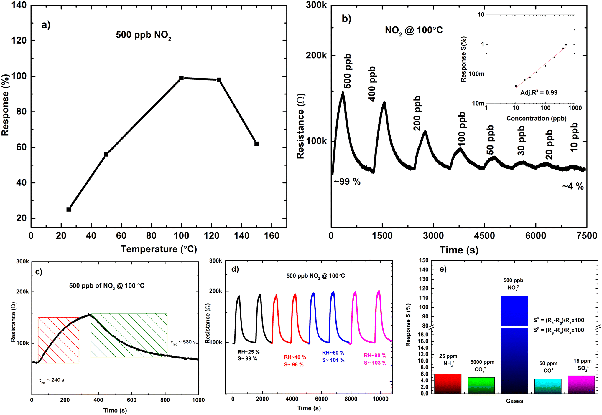 | ||
| Fig. 6 (a) Sensing performance of the inkjet-printed In2O3 microsensor at different temperatures for 500 ppb of NO2, (b) concentration variation study for NO2 at 100 °C (sensitivity curve in the inset), (c) the resistance transient for 500 ppb NO2 at 100 °C, (d) the effect of relative humidity on the sensing performance, and (e) selectivity against other gases at 100 °C. | ||
The inset in Fig. 6(b) provides a calibration curve plotting sensor response against NO2 concentration on a logarithmic scale. The linear relationship with an adjusted R2 value of 0.99 indicates excellent linearity and reliability of the sensor for quantifying NO2 concentrations. This linearity is crucial for accurate and reproducible measurements in practical applications. The resistance transient of the In2O3 sensor is depicted in Fig. 6(c), and the response and recovery times were determined to be approximately 240 s and 580 s, respectively. Moving along, Fig. 6(d) explores the sensor's performance under different relative humidity (RH) levels at a constant NO2 concentration of 500 ppb. The sensor maintains high sensitivity across all tested RH levels (25% to 92%), although the absolute response magnitude varies slightly. Furthermore, Fig. 6(e) assesses the sensor's selectivity by comparing its response to NO2 against other gases (NH3, CO2, CO, and SO2). The printed In2O3 sensor shows a significantly higher response to NO2 compared to other gases, confirming its high selectivity.
Fig. 7 illustrates the sensing characteristics of the printed SnO2 microsensor for NO2 detection. Fig. 7(a) depicts the sensor's response to 500 ppb NO2 at various operating temperatures. The SnO2-based sensor exhibits its highest response at room temperature (25 °C), with a response of approximately 652%. As the temperature increases, the response gradually decreases, indicating that lower temperatures favor NO2 detection for this sensor. This trend suggests that the sensor operates most effectively under ambient conditions, making it well-suited for low-temperature applications. The decline in response at higher temperatures could be attributed to reduced gas adsorption or increased desorption from the sensor surface, which diminishes sensitivity.
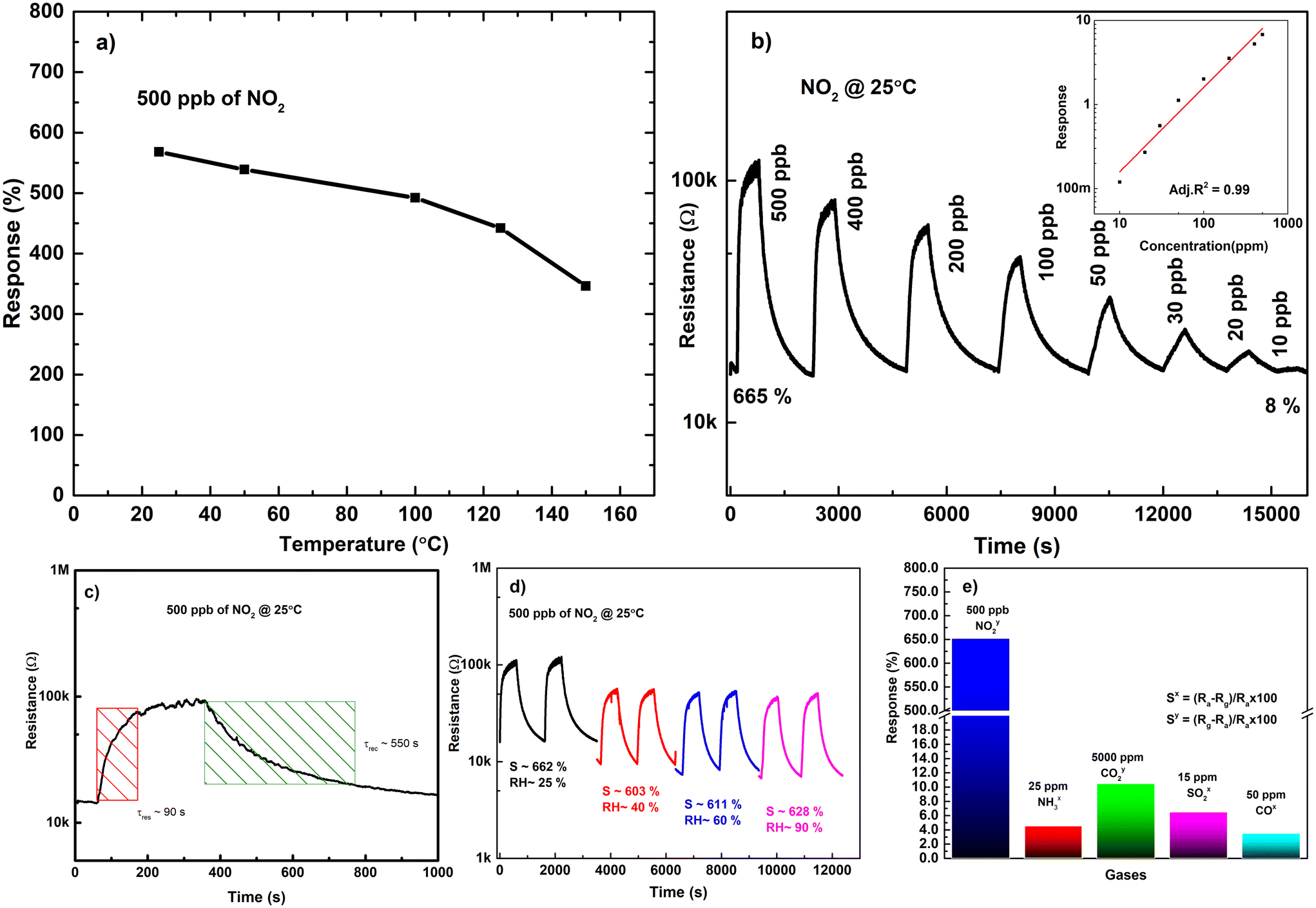 | ||
| Fig. 7 (a) Sensing performance of the inkjet-printed SnO2 microsensor at different temperatures for 500 ppb of NO2, (b) concentration variation study for NO2 at room temperature (sensitivity curve in the inset), (c) the resistance transient for 500 ppb NO2 at 25 °C, (d) the effect of relative humidity on the sensing performance, and (e) selectivity against other gases at 100 °C. | ||
Fig. 7(b) showcases the sensor's response to NO2 at different concentrations, ranging from 10 ppb to 500 ppb levels. A clear resistance change is observed for each concentration, demonstrating high sensitivity and a broad dynamic range. The percentage response increases with gas concentration, with a significant 652% response at 500 ppb NO2. The sensor maintains a noticeable response even at lower concentrations, confirming its capability to detect trace levels of NO2. The inset in Fig. 7(b) presents a calibration curve that plots sensor response against NO2 concentration, revealing a strong linear correlation with an adjusted R2 value of 0.99. This high linearity ensures accurate and reproducible measurements, which is crucial for gas sensing applications.
Furthermore, the SnO2 sensor exhibited a response time of about 80 s and a recovery time of approximately 540 s as shown in Fig. 7(c). Fig. 7(d) examines the sensor's behavior under varying relative humidity levels while being exposed to a constant NO2 concentration of 500 ppb. The sensor response remains stable across different RH levels (25% to 90%), although some variations are observed. The response values recorded at different RH levels include 603% at 40% RH, 611% at 60% RH, and 628% at 90% RH. Despite these variations, the sensor demonstrates reliable performance in humid environments, making it suitable for practical applications. Finally, Fig. 7(e) evaluates the selectivity of the sensor by comparing its response to NO2 against other gases such as CO2, NH3, SO2 and CO. The sensor exhibits a significantly stronger response to NO2 than to other interfering gases, confirming high selectivity. The minimal response to other gases suggests that the sensor is well-suited for NO2 detection with minimal cross-sensitivity.
The sensing data clearly indicate that the printed SnO2 sensor outperforms the printed In2O3 sensor. Therefore, its stability was evaluated over a one-month period. Fig. 8 presents the sensing data of the printed SnO2 microsensor at various intervals, demonstrating consistent performance with minimal degradation. Even after a month, the sensor maintains a stable response, highlighting its robustness and reliability for long-term applications.
 | ||
| Fig. 8 Stability of a printed SnO2 microsensor over the period of a month. | ||
The gas sensing mechanism is illustrated in Fig. S3.† When metal oxide is exposed to the atmosphere, oxygen molecules adsorb onto its surface. This adsorption process involves the transfer of electrons from the metal oxide lattice to the oxygen molecules. As oxygen molecules accept these electrons, they create an electron-deficient region on the sensor's surface, forming a depletion layer that increases the sensor's resistance.10 At lower temperatures, such as those in the current study, the most common oxygen anions on the metal oxide surface are O2−.36 In the presence of NO2, the gas molecules adsorb onto the sensor surface and undergo specific reactions,37,38 further affecting the sensor's electrical properties:
| NO2(gas) + e− ↔ NO2(ads)− | (2) |
| 2NO2(gas) + O2(ads)−2e− ↔ 2NO2(ads)−O(ads)− | (3) |
With the adsorption of NO2 molecules onto the surface, the depletion region on the sensor expands further because NO2 accepts electrons from the metal oxide conduction band, which increases the sensor's resistance.39 The difference in resistance between air and NO2 environments is measured to quantify the sensor response.
In the present study, the printed SnO2 sensor demonstrated excellent sensitivity at room temperature, along with a faster response time and higher overall responsiveness, attributed to its greater surface porosity and oxygen vacancy concentration, as confirmed by SEM and XPS analyses.4,29,40,41 These characteristics make it particularly suitable for low-power, ambient-condition applications. In contrast, the In2O3 sensor performed optimally at elevated temperatures (100 °C) and showed more stable behavior under humid conditions, making it a promising candidate for applications where temperature control is feasible and humidity resistance is critical. These combined factors contribute to the superior gas sensing performance of printed SnO2 over printed In2O3 at room temperature. Although the recovery times of the sensors may seem relatively slow, such behavior is typical of metal oxide gas sensors operating at low sensing temperatures.35,42,43 To improve the response and recovery characteristics, several strategies can be considered. These include surface functionalization with catalytic additives to enhance surface reactions and nanostructuring of the sensing material to increase the surface-to-volume ratio, thereby facilitating faster gas diffusion and adsorption/desorption kinetics.13,29,44
Both sensors exhibit good sensitivity across varying relative humidity (RH) levels. However, a slight variation in the baseline resistance is observed for both printed gas sensors, which can be attributed to the adsorption of water molecules on the sensor surface. Water molecules tend to replace the initially adsorbed oxygen species, leading to the release of trapped electrons back into the conduction band of the metal oxide. This process reduces the sensor's resistance, as previously reported in the literature.45,46 The humidity effect is more pronounced in SnO2, as its optimum sensing performance is achieved at room temperature, whereas the In2O3 sensor requires an elevated operating temperature of approximately 100 °C for optimal response.30 At room temperature, humidity has a greater impact on sensing due to the increased presence of physisorbed water molecules, which actively participate in the charge transfer process.47 In contrast, at higher temperatures, water molecules tend to desorb more readily, reducing their influence on the sensor's electrical properties. This explains the stronger humidity dependence observed in SnO2 compared to In2O3. The superior selectivity for NO2 is attributed to its higher electron affinity of 2.28 eV, compared to the lower electron affinity of pre-adsorbed oxygen at 0.43 eV and other gases.13,33
Table 2 presents a comparison of recent studies on NO2 sensing with the current work. The results clearly demonstrate that the inkjet-printed SnO2 microsensor offers performance that is either comparable to or surpasses those of previously reported sensors.
| Sl. no | Material | Temperature (°C) | Response | Concentration (ppb) | Ref. | |
|---|---|---|---|---|---|---|
| (%) |
|
|||||
| 1 | Inkjet-printed SnO2 | 175 | — | 11507 |
5000 | 18 |
| 2 | Inkjet-printed rGO/CuCoOx | RT | ∼70 | — | 1000 | 26 |
| 3 | SnSe nanoflakes | RT | — | 12.12 | 1000 | 48 |
| 4 | SnS2/Mo4/3B2 | RT | — | 4.82 | 1000 | 49 |
| 5 | Mo2CT2 | RT | 65 | — | 10000 |
43 |
| 6 | Inkjet-printed SnO2 | RT | ∼665 | 7.6 | 500 | This work |
| ∼8 | — | 10 | ||||

Conclusions
The presented research study demonstrates the potential of inkjet-printed metal oxide gas sensors for highly sensitive NO2 detection. The SnO2 sensor exhibited excellent room-temperature performance, detecting NO2 concentrations as low as 10 ppb, while the In2O3 sensor achieved optimal sensitivity at an elevated operating temperature of 100 °C. Both sensors showed a linear response to NO2, ensuring reliable and reproducible measurements. Although humidity variations slightly influenced baseline resistance, the sensors maintained strong selectivity for NO2 over other gases. These results underscore the viability of printed gas sensors for environmental monitoring applications, offering an efficient approach for air quality sensing.Author contributions
P. K. Shihabudeen: conceptualization, methodology, investigation, data curation, writing – original draft preparation, and writing – review & editing. Shivam Gupta: investigation and writing – review & editing. Yu-Hsien Lin: methodology and investigation. Shih-Wen Chiu: methodology and writing – review & editing. Yu Ting Chuang: methodology and investigation. Yuan Fu Tang: methodology and investigation. Nyan-Hwa Tai: resources and writing – review & editing. Kea-Tiong Tang: supervision, writing – review & editing, and funding acquisition.Data availability
All the data will be provided and made available upon request.Conflicts of interest
There are no conflicts to declare.Acknowledgements
The authors acknowledge the National Science and Technology Council (NSTC), Taiwan, for financial support of the work (NSTC 113-2218-E-007-019, MOST 111-2221-E-007-108-MY3 and NSTC 113-2640-E-007-005).References
- Q. Li, W. Zeng and Y. Li, Sens. Actuators, B, 2022, 359, 131579 CrossRef CAS.
- V. L. Patil, D. S. Dalavi, S. B. Dhavale, S. A. Vanalakar, N. L. Tarwal, A. S. Kalekar, J. H. Kim and P. S. Patil, New J. Chem., 2022, 46, 7588–7597 RSC.
- P. K. Shihabudeen, S. Gupta, M. Y. Notash, J. J. Sardroodi, S.-W. Chiu, N.-H. Tai and K.-T. Tang, Sens. Actuators, B, 2023, 394, 134438 CrossRef CAS.
- K. Sun, G. Zhan, L. Zhang, Z. Wang and S. Lin, Sens. Actuators, B, 2023, 379, 133294 Search PubMed.
- Z. Yang, L. Jiang, J. Wang, F. Liu, J. He, A. Liu, S. Lv, R. You, X. Yan, P. Sun, C. Wang, Y. Duan and G. Lu, Sens. Actuators, B, 2021, 326, 128828 CrossRef CAS.
- S. Hussain, A. N. Begi, J. N. O. Amu-Darko, K. Yusuf, R. K. Manavalan, A. Iqbal, X. Zhang, G. Qiao and G. Liu, Sens. Actuators, B, 2024, 420, 136489 CrossRef CAS.
- S. Hussain, S. Wang, J. N. O. Amu-Darko, A. N. Begi, K. Yusuf, T. K. Ibrahim, A. Iqbal, R. K. Manavalan, X. Zhang and G. Qiao, Sens. Actuators, B, 2025, 425, 136954 CrossRef CAS.
- S. Hussain, S. El-Ouardy, A. N. Begi, K. Yusuf, B. Aslam, A. Shaheen, A. Rabnawaz, N. Farooq, R. K. Manavalan, G. Liu, X. Zhang and G. Qiao, Mater. Sci. Semicond. Process., 2024, 184, 108825 CrossRef CAS.
- S. Hussain, L. Peng, J. N. O. Amu-Darko, A. Shahid, K. Yusuf, S. Wang, M. J. Liaqat, R. K. Manavalan, X. Zhang and G. Qiao, Mater. Sci. Semicond. Process., 2024, 184, 108840 CrossRef CAS.
- H. Ma, L. Yu, X. Yuan, Y. Li, C. Li, M. Yin and X. Fan, J. Alloys Compd., 2019, 782, 1121–1126 CrossRef CAS.
- Y. Masuda, Sens. Actuators, B, 2022, 364, 131876 CrossRef CAS.
- P. Xu, Z. Cheng, Q. Pan, J. Xu, Q. Xiang, W. Yu and Y. Chu, Sens. Actuators, B, 2008, 130, 802–808 CrossRef CAS.
- Z. Jin, C. Wang, L. Wu, H. Song, X. Yao, J. Liu, J. Zhao, Z. Zeng and F. Wang, Sens. Actuators, B, 2023, 377, 133058 CrossRef CAS.
- A. R. Nimbalkar, N. B. Patil, V. V. Ganbavle, S. V. Mohite, K. V. Madhale and M. G. Patil, J. Alloys Compd., 2019, 775, 466–473 CrossRef CAS.
- P. K. Shihabudeen and A. R. Chaudhuri, Sens. Actuators, B, 2020, 305, 127523 CrossRef CAS.
- T.-C. Wu, A. De Luca, Q. Zhong, X. Zhu, O. Ogbeide, D.-S. Um, G. Hu, T. Albrow-Owen, F. Udrea and T. Hasan, npj 2D Mater. Appl., 2019, 3, 42 CrossRef CAS.
- O. Kassem, M. Saadaoui, M. Rieu and J.-P. Viricelle, J. Mater. Chem. C, 2019, 7, 12343–12353 RSC.
- N. Devabharathi, A. M. Umarji and S. Dasgupta, ACS Appl. Mater. Interfaces, 2020, 12, 57207–57217 CrossRef CAS PubMed.
- X. Peng, J. Liu, Y. Tan, R. Mo and Y. Zhang, Sens. Actuators, B, 2022, 362, 131775 CrossRef CAS.
- A. Sajedi-Moghaddam, E. Rahmanian and N. Naseri, ACS Appl. Mater. Interfaces, 2020, 12, 34487–34504 CrossRef CAS PubMed.
- X. Peng, J. Yuan, S. Shen, M. Gao, A. S. R. Chesman, H. Yin, J. Cheng, Q. Zhang and D. Angmo, Adv. Funct. Mater., 2017, 27, 1703704 CrossRef.
- J. Li, F. Rossignol and J. Macdonald, Lab Chip, 2015, 15, 2538–2558 RSC.
- L. Vigna, A. Verna, S. L. Marasso, M. Sangermano, P. D'Angelo, F. C. Pirri and M. Cocuzza, Sens. Actuators, B, 2021, 345, 130381 CrossRef CAS.
- X. Wang, M. Wei, X. Li, S. Shao, Y. Ren, W. Xu, M. Li, W. Liu, X. Liu and J. Zhao, ACS Appl. Mater. Interfaces, 2020, 12, 51797–51807 CrossRef CAS PubMed.
- L. Huang, Z. Wang, J. Zhang, J. Pu, Y. Lin, S. Xu, L. Shen, Q. Chen and W. Shi, ACS Appl. Mater. Interfaces, 2014, 6, 7426–7433 CrossRef CAS PubMed.
- O. Ogbeide, G. Bae, W. Yu, E. Morrin, Y. Song, W. Song, Y. Li, B. Su, K. An and T. Hasan, Adv. Funct. Mater., 2022, 32, 2113348 CrossRef CAS.
- Z. Li, S. H. Sie, J. L. Lee, Y. R. Chen, T. I. Chou, P. C. Wu, Y. T. Chuang, Y. T. Lin, I. C. Chen, C. C. Lu, Y. Z. Juang, S. W. Chiu, C. C. Hsieh, M. F. Chang and K. T. Tang, in Technical Digest – International Electron Devices Meeting, IEDM, Institute of Electrical and Electronics Engineers Inc., 2021, vol. 2021-December, pp. 35.2.1–35.2.4.
- P. K. Shihabudeen and A. R. Chaudhuri, Nanoscale, 2022, 14, 5185–5193 RSC.
- J. Li, M. Yang, X. Cheng, X. Zhang, C. Guo, Y. Xu, S. Gao, Z. Major, H. Zhao and L. Huo, J. Hazard. Mater., 2021, 419, 126414 CrossRef CAS PubMed.
- M. Verma, G. Bahuguna, A. Saharan, S. Gaur, H. Haick and R. Gupta, ACS Appl. Mater. Interfaces, 2023, 15, 5512–5520 CrossRef CAS PubMed.
- Y.-X. Zhen, B.-Y. Song, W.-X. Liu, J.-X. Ye, X.-F. Zhang, Z.-P. Deng, L.-H. Huo and S. Gao, Sens. Actuators, B, 2022, 363, 131852 CrossRef CAS.
- H. Wu, X. Gong, W. Tao, L. Zhao, T. Wang, F. Liu, X. Yan, P. Sun and G. Lu, Sens. Actuators, B, 2023, 380, 133322 CrossRef CAS.
- H. Jiang, Y. Qu, X. Zhang, R. Gao, X. Cheng, S. Gao, L. Huo, Z. Major and Y. Xu, Appl. Surf. Sci., 2022, 590, 153033 CrossRef CAS.
- D. Han, L. Zhai, F. Gu and Z. Wang, Sens. Actuators, B, 2018, 262, 655–663 CrossRef CAS.
- S. Gasso, M. K. Sohal and A. Mahajan, Sens. Actuators, B, 2022, 357, 131427 CrossRef CAS.
- J.-Y. Kang, W.-T. Koo, J.-S. Jang, D.-H. Kim, Y. J. Jeong, R. Kim, J. Ahn, S.-J. Choi and I.-D. Kim, Sens. Actuators, B, 2021, 331, 129371 CrossRef CAS.
- F. Guo, C. Feng, Z. Zhang, H. Wu, C. Zhang, X. Feng, S. Lin, C. Xu, B. Zhang and H. Bai, Sens. Actuators, B, 2022, 364, 131898 CrossRef CAS.
- W. Oum, A. Mirzaei, T. Hussain, J. H. Bang, S. Han, K. Y. Shin, D. J. Yu, S. Kang, T. Kaewmaraya, S. S. Kim and H. W. Kim, Sens. Actuators, B, 2022, 363, 131853 CrossRef CAS.
- S. Ying, Y. Wang, Z. Wu, M. Huang, L. Dong, J. Zhao and C. Peng, Appl. Surf. Sci., 2021, 566, 150720 CrossRef CAS.
- M. S. Choi, M. Y. Kim, A. Mirzaei, H.-S. Kim, S. Kim, S.-H. Baek, D. W. Chun, C. Jin and K. H. Lee, Appl. Surf. Sci., 2021, 568, 150910 CrossRef.
- Y. Zhong, W. Li, X. Zhao, X. Jiang, S. Lin, Z. Zhen, W. Chen, D. Xie and H. Zhu, ACS Appl. Mater. Interfaces, 2019, 11, 13441–13449 CrossRef CAS PubMed.
- F. Guo, C. Feng, Z. Zhang, L. Zhang, C. Xu, C. Zhang, S. Lin, H. Wu, B. Zhang, A. Tabusi and Y. Huang, Sens. Actuators, B, 2023, 375, 132885 CrossRef CAS.
- B. Wang, X. Gao, J. He, Y. Xiao, Y. Liu, X. Jia, K. Zhang, C. Wang, P. Sun, F. Liu and G. Lu, Sens. Actuators, B, 2024, 399, 134790 CrossRef CAS.
- Z. Dai, L. Xu, G. Duan, T. Li, H. Zhang, Y. Li, Y. Wang, Y. Wang and W. Cai, Sci. Rep., 2013, 3, 1669 CrossRef PubMed.
- C. Yuan, J. Ma, Y. Zou, G. Li, H. Xu, V. V. Sysoev, X. Cheng and Y. Deng, Adv. Sci., 2022, 035, 94 Search PubMed.
- A. Staerz, U. Weimar and N. Barsan, Sens. Actuators, B, 2022, 358, 131531 CrossRef CAS.
- H. Zhu, Q. Li, Y. Ren, Q. Gao, J. Chen, N. Wang, J. Deng and X. Xing, Small, 2018, 14, e1703974 CrossRef PubMed.
- R. Samui, S. Acharyya, A. K. Bhunia, S. Saha and P. K. Guha, ACS Appl. Nano Mater., 2024, 7, 24281–24290 CrossRef CAS.
- W. Zhang, W. Wang, Y. Ge, L. Sun, C. Zhou, Y. Sun and J. Hu, Sens. Actuators, B, 2024, 420, 136496 CrossRef CAS.
Footnote |
| † Electronic supplementary information (ESI) available. See DOI: https://doi.org/10.1039/d5nr00694e |
| This journal is © The Royal Society of Chemistry 2025 |