
 Open Access Article
 This Open Access Article is licensed under a Creative Commons Attribution-Non Commercial 3.0 Unported Licence
Interfacial chalcogen pair-mediated, biaxial strain- and interlayer distance-tuneable type-2 band alignment in an SnSSe homogeneous bilayer: a density functional theory-based analysis†
Naresh
Bahadursha
a,
Chanda
Bhavitha Sri
a,
Kuna Krishna
Ruthvik
a,
Swastik
Bhattacharya
b and
Sayan
Kanungo
 *ac
*ac
aElectrical and Electronics Engineering Department, Birla Institute of Technology and Science-Pilani, Hyderabad Campus, Hyderabad-500078, India. E-mail: sayan.kanungo@hyderabad.bits-pilani.ac.in
bDepartment of Physics, Birla Institute of Technology and Science-Pilani, Hyderabad Campus, Hyderabad, 500078, India
cMaterials Center for Sustainable Energy & Environment, Birla Institute of Technology and Science-Pilani, Hyderabad Campus, India
First published on 29th May 2025
Abstract
This study presents a comprehensive density functional theory-based investigation of the electronic properties of homogeneous bilayer Janus tin sulphide selenide (SnSSe) with different interfacial chalcogen pair configurations. This study focuses on interlayer band alignment, wherein the effects of interlayer distance modulation and applied biaxial strain are methodically studied. Next, the spatial distribution and lifetime of excitonic states are systematically analysed from the in-plane and inter-layer atomic orbital interactions, spatial separation of electron–hole wave functions, and spread of the conduction band in energy. Asymmetric interfacial chalcogen pairing exhibits a finite interlayer dipole moment and interlayer electric field. This reduces the energy bandgap and induces prominent type-2 band alignment between individual SnSSe layers, where band edge Bloch states are strongly localized in alternating layers. An increasing interlayer distance and applied biaxial tensile strain were found to retain the type-2 interlayer band alignment. In contrast, reducing the interlayer distance and biaxial compressive strain significantly altered interlayer atomic orbital interactions and annihilated the type-2 band alignment with a sharp reduction in the energy bandgap owing to the strong delocalization of band edge Bloch states. Thus, this study demonstrates the strain tuneable type-2 band alignment and interlayer excitonic properties of homogeneous bilayer SnSSe with broken interlayer mirror symmetry.
1. Introduction
Recently, the successful realization of a large number of two-dimensional (2D) materials with distinct and unique physicochemical properties has shown the potential to reshape the technological landscape, spanning conventional applications such as electronics, optoelectronics, sensing, photonics, and energy storage as well as emerging applications such as spintronics and valleytronics.1–5 Moreover, an ever-increasing research effort has been observed towards tuning the relevant properties of 2D materials using different material engineering strategies, leading to novel 2D material systems for specific applications.6,7 In this context, breaking one or more underlying symmetries in 2D materials has shown remarkable promise for harvesting emergent electronic/optoelectronic/magnetic/spintronic properties in such engineered 2D materials.7,8 Some of the most notable examples of such approaches include out-of-plane electric field and staggered substrate sub-lattice potential induced inversion symmetry breaking in bilayer graphene, interlayer twisting induced inversion symmetry breaking in bilayer transition metal di-chalcogenides (TMDs), magnetic field induced time reversal symmetry breaking in phosphorene, magnetic substrate induced time reversal symmetry breaking in TMDs, and carrier doping induced gauge symmetry breaking in TMDs.7,9 In this effect, recently, the successful synthesis of 2D Janus metal dichalcogenides (JMDs), an artificial subclass of metal dichalcogenides (MDs), has paved the path for inherently breaking the out-of-plane (OOP) intra-layer mirror symmetry in monolayer MDs.10,11 Unlike natural MDs, in JMDs, the metal is covalently bonded to two different chalcogen atoms, breaking mirror symmetry in the OOP direction around the metal atom centre. Furthermore, owing to the different electronegativities of chalcogen atoms, the asymmetric valence charge distributions in the top and bottom chalcogen layers result in a vertical intralayer electric field in JMDs.9 Specifically, the vertical intralayer electric field and natural OOP asymmetry in JMDs significantly influence their electronic/optoelectronic properties. The vertical intralayer electric field in JMDs reduces electron–hole wavefunction overlapping and increases Coulomb screening, leading to longer exciton lifetimes, wherein the natural OOP symmetry breaking in JMDs results in strong Rashba spin–orbit coupling (SOC).7,9MoSSe was the first JMD to be synthesized following the chemical vapor deposition (CVD) technique in 2017.12,13 During MoSSe synthesis, either the top S-layer of the monolayer MoS2 is first substituted with H, followed by selenization through vaporization of Se powders,12 or sulfurization of the top Se-layer of the MoSe2 monolayer.13 In this effect, an alternative room-temperature synthesis process for MoSSe and WSSe was demonstrated using a selective epitaxy atomic replacement process that efficiently removes and thereafter substitutes the top chalcogen layer.14 Motivated by these advancements in group VIB, i.e. Molybdenum- and Tungsten-based JMD synthesis, several reports have attempted to synthesize other JMDs. Notably, among non-group VIB JMDs, tin (Sn)-based JMDs have drawn significant research attention, wherein the successful synthesis of SnSSe has recently been reported using hot injection of Se precursor and S precursor solutions into the Sn precursor15 and plasma-driven selenization.16
However, research on Sn-based JMDs is still at an early stage, and a comprehensive theoretical understanding of the electronic and optoelectronic properties of these emerging artificial 2D materials is necessary for their effective integration into different devices. In this context, density functional theory (DFT)-based ab initio calculation has emerged as a highly efficient theoretical modelling technique for 2D material systems that can independently estimate the different properties of 2D materials and assess the efficacy of different material engineering strategies for tuning the relevant properties of specific 2D materials. This has led to DFT-based theoretical investigations of different Sn-based JMDs, including SnSSe, SnSeTe, and SnSTe. Recent DFT studies have demonstrated that SnSSe, SnSeTe, and SnSTe monolayers are thermally, dynamically, and mechanically stable.17,18 Notably, SnSTe and SnSeTe monolayers exhibit metallic behaviour, whereas SnSSe monolayers exhibit indirect semiconducting characteristics.18,19 This has drawn significant research interests in SnSSe, where the broken OOP mirror symmetry of SnSSe can be exploited for different electronic, optoelectronic, piezoelectric, thermoelectric, and sensing applications.18,20–22 Specifically, recent DFT investigations have revealed that the electronic properties of monolayer SnSSe can be efficiently tuned by applying mechanical strain,20,23 out-of-plane direction electric field,23 surface adatom adsorption,24 and vacancy engineering.25
On the other hand, very recently, the homogeneous (consisting of the same JMD monolayers) and heterostructure (consisting of different JMD monolayers) bi-layer configuration of JMDs has drawn significant traction from researchers, as the interlayer stacking configuration is found to play a crucial role in determining the overall electronic/optoelectronic properties of bilayer JMDs.26–30 To this effect, the homogeneous bilayers of JMDs offer additional design flexibility regarding their formation with respect to interfacial chalcogen pair specification in specific interlayer stacking configurations. The asymmetric interfacial chalcogen pair breaks the interlayer mirror symmetry around the interface, which can lead to emerging electronic and optoelectronic properties in such homogeneous bilayers.27–29,31–33 However, to date, only a few reports are available on the bilayer Janus SnSSe.29,30,34,35 Typically, strong anharmonic phonon scattering,34 non-zero dipole moments induced built-in electric fields,30 interlayer stacking-dependent exciton binding energies,29 and interlayer twisting-dependent lattice thermal conductivity35 are theoretically demonstrated in bilayer SnSSe. However, to the best of the authors’ knowledge, no reports have attempted to investigate the effects of mechanical strain on bilayer SnSSe, focusing on the effects of strain-mediated modulation in interlayer atomic orbital interactions on the electronic properties of bilayer SnSSe. On the other hand, several theoretical and experimental studies have focused on interlayer excitons in vdW heterostructure TMD bilayers.36–39 Specifically, it has been observed that interlayer excitons are highly sensitive to interlayer interactions, and thereby can be efficiently tuned by applying strain or varying interlayer distance by either inserting an insulating layer (usually h-BN) or applying pressure.36,38–40 In this context, the homogeneous bilayers of Janus TMDs exhibit both symmetric and asymmetric interfacial chalcogen pairings in their different interlayer stacking configurations.29,33 The broken out-of-plane mirror symmetry along the interface of bilayer Janus TMDs offers a unique possibility of realizing type-2 band alignment and subsequent interlayer excitons under an asymmetric interfacial chalcogen pairing configuration.33 However, to the best of the authors’ knowledge, to date, no theoretical or experimental studies have exclusively analyzed the effects of strain and interlayer distance variation on the properties of interlayer excitons in homogeneous bilayers of Janus TMDs.
Based on this paradigm, in this study, the structural and electronic properties of homogeneous bilayer SnSSe in different interfacial chalcogen pair configurations are extensively studied, emphasizing interlayer charge transfer, dipole moment, electric field, and band alignment at different interfacial chalcogen pairings. Moreover, this study systematically investigates the electronic properties of bilayer SnSSe with asymmetric chalcogen pairing at various interlayer distances under biaxial strain. The key findings of this study are methodically analysed from atomic electronegativity-mediated localized charge distributions, inter-layer atomic orbital interactions, and band edge electronic state localization. In this context, the novelty of this study can be summarized as follows:
1. In this study, for the first time, it was demonstrated that the interlayer band alignment, bandgap and excitonic properties can be efficiently tuned by varying the interlayer distance and applying biaxial mechanical strain in asymmetric interfacial chalcogen pairing in Janus TMD bilayers.
2. This study introduces a novel approach by systematically analyzing the electronic and excitonic property variations with interlayer distance and applying biaxial strain from the time-energy uncertainty relation near the band edges, spatial localization and overlap of electron and hole wave functions, and interlayer intrinsic electric field.
Finally, the specific contributions of this research in the context of existing theoretical research on other Janus TMD bilayers are summarized in Table 1.
| Material specification | Ab initio DFT methods | Key findings | Ref. |
|---|---|---|---|
| 2L-MoSSe | GGA-PBE | Strain engineering enhances Li diffusion in bilayer | 41 |
| 2L-MoSSe | GGA-PBE | Interlayer stacking engineering can tune the interlayer dipole moments and carrier mobilities | 42 |
| 2L-MoSeTe and 2L-WSeTe | GGA-PBE | Rashba spin splitting at the band edges can be tuned using strain engineering | 43 |
| 2L-WSSe | GGA-PBE | Bandgap and optical anisotropy control using strain engineering | 44 |
| 2L-SnSSe | GW | Interlayer stacking engineering can tune the energy bandgap and excitonic binding energies | 29 |
| 2L-SnSSe | GGA-PBE | Interlayer stacking engineering can tune the interlayer dipole moment/electric field and carrier mobility | 30 |
| 2L-SnSSe [this work] | HSE-06 | Strain and interlayer distance engineering to tune interlayer band alignment, bandgap and excitonic lifetime by changing in-plane and out-of-plane orbital hybridization, and electron–hole wave function overlap | — |
Next, the organization of the subsequent sections of this paper is summarized. Section 2 provides a comprehensive overview of the computational methodology, highlighting the simulation methods and parameters used in the DFT simulations and the parameter definitions used to quantify the relevant material properties. The reliability of the simulation framework was verified by calibrating the calculated structural and electronic properties in accordance with previous literature. Section 3 incorporates a comprehensive stability analysis of the individual bilayers, followed by a detailed account of their structural and electronic properties. Furthermore, in this section, the impact of externally applied biaxial strain and interlayer distance variations on electronic properties is explored in detail, providing a systematic analysis of the key findings in relation to fundamental atomistic characteristics. Finally, section 4 summarizes the primary outcomes of this study, discusses their significance for potential technological applications, and suggests avenues for future explorations.
2. Computational methodology
This section presents the computational methodology of this study, in which the material specifications, simulation framework, and analytical parameter definition are discussed in three sub-sections.2.1. Material specifications
This study focused on the bilayer of Janus tin sulphide selenide (2L-SnSSe). The monolayer tin di-sulphide (SnS2) and tin di-selenide (SnSe2) belong to P![[3 with combining macron]](https://www.rsc.org/images/entities/char_0033_0304.gif) m1 space group with a hexagonal lattice structure, exhibiting mirror symmetry around the central Sn atom,29 as shown in Fig. 1a and b. However, due to the asymmetrical chalcogen composition of their Janus counterpart, i.e. SnSSe lacks mirror symmetry and belongs to a symmetry-reduced P3m1 space group with a hexagonal lattice structure,29 as shown in Fig. 1c. For the formation of bilayer SnSSe, the natural stacking order of bilayer SnS2 and SnSe2 is considered in this study, where the Sn atom of the top layer is perfectly aligned with the Sn of the bottom monolayer. This suggests that during bilayer SnSSe formation, three distinct interlayer stacking configurations can be considered based on the interlayer chalcogen pairing layers (i.e. S–S, S–Se, and Se–Se) between two monolayers of SnSSe. In their earlier study, the authors reported that interlayer chalcogen pairing plays a vital role in determining the overall electronic properties of any bilayer on Janus TMDs.26
m1 space group with a hexagonal lattice structure, exhibiting mirror symmetry around the central Sn atom,29 as shown in Fig. 1a and b. However, due to the asymmetrical chalcogen composition of their Janus counterpart, i.e. SnSSe lacks mirror symmetry and belongs to a symmetry-reduced P3m1 space group with a hexagonal lattice structure,29 as shown in Fig. 1c. For the formation of bilayer SnSSe, the natural stacking order of bilayer SnS2 and SnSe2 is considered in this study, where the Sn atom of the top layer is perfectly aligned with the Sn of the bottom monolayer. This suggests that during bilayer SnSSe formation, three distinct interlayer stacking configurations can be considered based on the interlayer chalcogen pairing layers (i.e. S–S, S–Se, and Se–Se) between two monolayers of SnSSe. In their earlier study, the authors reported that interlayer chalcogen pairing plays a vital role in determining the overall electronic properties of any bilayer on Janus TMDs.26
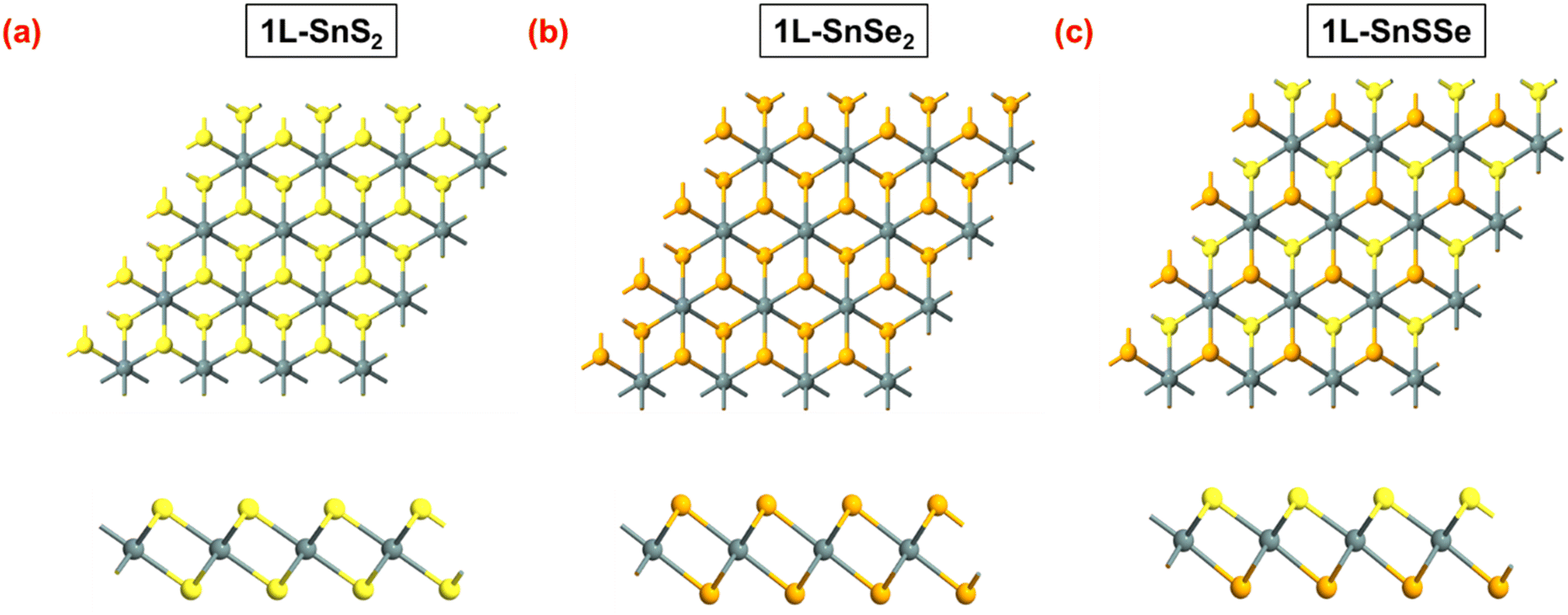 | ||
| Fig. 1 Schematic representation of the top and side views of a 4 × 4 × 1 super-cell of (a) 1L-SnS2, (b) 1L-SnSe2, and (c) 1L-SnSSe. | ||
The presence of two different chalcogen atoms in SnSSe indicates that three distinct interface chalcogen pair configurations are possible during bilayer formation.29 Subsequently, in this study, the bilayers of SnSSe are considered in the natural interlayer stacking order (AA) of bilayer SnS2 and SnSe2, with S–S, S–Se, and Se–Se interlayer chalcogen pairings, in their unit cell (1 × 1 × 1) configurations. A previous theoretical study on different artificial and natural SnSSe bilayer stacking orders demonstrated that the natural stacking order is the most stable (with the lowest formation energy) stacking order of bilayer SnSSe.29 Hence, only the natural AA stacking order was considered in this study. In addition, unlike van der Waals (vdW) hetero-bilayers, the three distinct bilayers of SnSSe considered in this study form homogeneous bilayers, where no lattice mismatch strain can be observed, and the unit-cell configuration should suffice for the theoretical analysis. Furthermore, a vacuum of 40 Å is considered in the out-of-plane direction of the unit cells of SnS2, SnSe2, and SnSSe monolayers and bilayers to ensure no artificial interaction from the periodic images in these directions.29,35 Similar to monolayers of SnSSe, natural bilayers of SnSSe also exhibit a hexagonal lattice structure, preserving the hexagonal symmetry of their Brillouin zone. Consequently, the Brillouin zone of all the monolayers and bilayers under investigation in this study was sampled across the characteristic G–M–K–G high symmetry path for energy band structure calculations.
2.2. Simulation framework
This study investigates the structural and electronic properties of materials using first-principles calculations implemented through the Atomistix Tool Kit (ATK) and Virtual Nano Lab (VNL) simulation packages, available from Synopsys Quantum Wise.45 The first-principal calculations employ a linear combination of atomic orbitals (LCAO) with a PseudoDojo basis set, utilizing a density mesh cut-off energy of 125 Hartree and a 12 × 12 × 1 Monkhorst–Pack grid for sampling the Brillouin zone.45 Initially, the individual unit cells of monolayers and bilayers of SnSSe are structurally relaxed to minimize the total energy and the forces acting on individual atoms using geometry optimization. This optimization was performed using the limited-memory Broyden–Fletcher–Goldfarb–Shanno (LBFGS) algorithm, with pressure and force tolerances set at 0.0001 eV Å−3 and 0.01 eV Å−1, respectively.45 Furthermore, during geometry optimization, the Generalized Gradient Approximation (GGA) method with the Perdew–Burke–Ernzerhof (PBE) exchange–correlation functional is considered.45 The structural parameters of the optimized monolayers for SnS2, SnSe2, and SnSSe are illustrated in Fig. S1.†The energetics of individual monolayer materials were also calculated using the GGA method with the PBE exchange–correlation functional.45 For the energy calculations of bilayers, the Grimme DFT-D3 method is employed to accurately account for the vdW interactions between the monolayers, while the counterpoise (CP) correction is applied to mitigate the basis set superposition error (BSSE) inherent in the LCAO basis.45 Standard DFT methods, such as LDA-PZ and GGA-PBE, tend to underestimate the energy bandgaps of layered materials due to self-interaction errors.45 Consequently, to attain a more precise assessment of the energy band structures for the geometry-optimized monolayers and homogeneous bilayers, electronic properties were computed using the advanced Heyd–Scuseria–Ernzerhof-06 (HSE-06) method following geometry optimization. Next, the HSE-06 calculated energy bandgaps were compared against existing literature, as summarized in Table 2, which shows reasonable agreement with previously reported HSE calculated bandgap values.25,46–49 The standard DFT functional, such as GGA, tends to underestimate the bandgaps of 2D semiconductors like SnSSe. However, the advanced HSE-06 functional offers a more accurate assessment of the energy bandgap of 2D semiconductors.50 Moreover, the HSE-06 functional is widely considered in the theoretical literature for estimating the energy band structures of monolayer and few-layer SnS2, SnSe2,47 SnSSe20,29,34,51 and some other Janus TMDs.52–55 Consequently, in this study, the energy band structures are simulated using HSE-06 (with SOC). Finally, in this study, the dynamic stability of bilayers with these chalcogen pairings was investigated using phonon spectrum calculations performed on a 4 × 4 × 1 supercell of bilayers,29 with a maximum displacement set at 0.01 Å, using the phonopy code.56 To estimate the thermal stability of the bilayers of these chalcogen pairings, the Nose–Hoover thermostat-based Ab initio molecular dynamic (AIMD) simulations were performed at room temperature (300 K) in a 4 × 4 × 1 supercell for 1000 time steps with a total time evaluation of 10 Pico-sec.57
| Material | Calculated (reported) bond length of M–X (Å) | Calculated (reported) bond angle X–M–X (°) | Calculated (reported) lattice constant (Å) | Calculated (reported) bandgap (eV) |
|---|---|---|---|---|
| 1L-SnS2 | 2.61 (2.59)46 | 89.51 (90.81)46 | 3.71 (3.70)46 | 2.20 (2.40)47 |
| 1L-SnSe2 | 2.78 (2.73)46 | 90.98 (90)48 | 3.83 (3.86)49 | 1.35 (1.41)47 |
| 1L-SnSSe | Sn–S: 2.65 (2.63), Sn–Se: 2.75 (2.72)25 | 89.82 (89.90°)25 | 3.82 (3.78)25 | 1.44 (1.46)25 |
In this study, following the theoretical literature, a standard strain range of −5% to +5% is considered. Specifically, theoretically ±10% biaxial strain in monolayer SnSSe,23 ±10% biaxial strain in monolayer SnS2,58 and +5% biaxial strain in monolayer MoSSe59 have been reported in the literature. Moreover, experimentally, monolayer MoS2 is subjected to 3% biaxial strain,60 5.6% biaxial strain,61 bilayer MoS2 is subjected to 2.2% uniaxial strain,62 3% uniaxial strain,63 and bilayer WSe2 is subjected to 5% uniaxial strain.64 These theoretical and experimental reports suggest that the ±5% biaxial strain can be considered a standard range of strain for bilayer SnSSe. Next, in the theoretical literature, −0.3 Å to +0.4 Å ILD variation has been reported for bilayer MoSSe,31 wherein experimental observations indicate interlayer separations reaching up to ∼0.68 nm (6.8 Å) in MoTe2.65 However, in few-layered 2D materials, experimentally, the interlayer distances can be effectively tuned to a larger extent by either inserting an insulating layer (usually h-BN) or applying pressure.36,38–40 Consequently, in this study, the ILD variation is considered within a reasonable range between −1.5 Å to +1.5 Å for SnSSe bilayers.
2.3. Theoretical model validation
To ensure the consistency and accuracy of the computational framework, a comprehensive validation procedure was implemented through systematic comparison with previous computational reports. This validation process focused on the structural, electrostatic, and electronic properties to verify the reliability of the theoretical calculation framework of this study. The optimized structural parameters (in-plane lattice vector, Sn–S/Sn–Se bond length, and S–Sn–Se bond angle) were compared with existing literature values, as summarized in Table 2. Notably, the calculated structural parameters showed good agreement with previously reported structural properties,25,46–49 confirming the reliability of the geometry optimization framework used in this study.Next, for SnSSe bilayers, the calculated lattice vectors of 3.86 Å, Sn–S bond lengths of 2.66 Å, and Sn–Se bond lengths of 2.76 Å are also in reasonable agreement with the reported lattice vectors of 3.77 Å, Sn–S bond lengths of 2.62 Å, and Sn–Se bond lengths of 2.71 Å.34 Furthermore, the calculated inter-layer distances of 2.70 Å (S–S), 2.81 Å (S–Se), 2.97 Å (Se–Se) are also in good agreement with previously reported inter-layer distances of 2.83 Å (S–S), 2.92 Å (S–Se), 2.99 Å (Se–Se).29 For SnSSe bilayers, the HSE calculated bandgap values of 1.49 eV (S–S), 1.47 eV (Se–Se), and 1.27 eV (S–Se) are consistent with previously reported HSE-06-SOC simulated bandgap values of 1.37 eV (S–S), 1.40 eV (Se–Se), and 1.26 eV (S–Se).34 Furthermore, similar to previous theoretical reports, each SnSSe bilayer exhibits an indirect bandgap, with the CBM located at the ‘M’ point and the ‘VBM’ at the ‘G’ point.29,34 Finally, for the S–Se configuration of the SnSSe bilayer, the calculated interlayer electric field of 0.14 V Å−1 and interlayer dipole moment of 0.27 D are also comparable to the previously reported electric field of 0.18 V Å−1 (ref. 29) and interlayer dipole moment of 0.27 D.30 Thus, the close agreement of the calculated structural, electrostatic, and electronic parameters with those of previous reports confirms the reliability of the computational framework of this study.
2.4. Parameter definitions
In this study, the structural stability of natural SnSSe bilayers was quantified using two key metrics: the cohesive energy per unit atom (Ecoh) and the interlayer interaction energy per unit in-plane area (Einterlayer_interaction), which are defined as.26 | (1) |
 | (2) |
In eqn (1), Ebilayer and ESn denote the ground-state energies of the vdW bilayer and an isolated Sn atom, respectively. Similarly, Echi,i=1–4 represents the ground-state energies of individual chalcogen atoms (i = 1–4) within the bilayer. In eqn (2), Emonolayer,j=1,2 represents the ground-state energies of the individual monolayers (j = 1–4), and Area is the in-plane unit cell area of the bilayer. For a structurally stable 2D crystal, the cohesive energy (Ecoh) must be negative, i.e. Ecoh < 0. Similarly, stable bilayer formation requires a negative interlayer interaction energy (Einterlayer_interaction), i.e. Einterlayer_interaction < 0. Moreover, larger magnitudes of Ecoh and Einterlayer_interaction indicate superior structural stability and interlayer binding strength of the bilayers, respectively.
The formation of heterostructure bilayers usually involves charge transfer between the constituent monolayers.26 Similarly, in this study, interlayer charge transfer (Qtransfer_layer) between individual SnSSe monolayers was considered for individual bilayer SnSSe configurations. The charge transfer is quantified through Mulliken charge analysis, which assigns partial charges to individual atoms in any material system.26 The Qtransfer_layer is represented by:
| QTransfer\_layer = Qmonolayer\_in\_bilayer − Qmonolayer | (3) |
In eqn (3), Qmonolayer_in_bilayer and Qmonolayer represent the total Mulliken charges in the monolayer SnSSe within the bilayer and in the isolated monolayers, respectively. In this context, Qtransfer_layer > 0 indicates that one monolayer is accepting electrons from another, whereas the other monolayer donates electrons corresponding to Qtransfer_layer < 0.
Similarly, the local charge redistributions during lattice formation can be accessed from the Mulliken charge transfer with respect to each atom (Qtransfer_atom) in Janus monolayers and bilayers, which is expressed as:
| Qtransfer\_atom = Qlattice − Qisolated | (4) |
In eqn (4), Qlattice denotes the Mulliken charge of the atom within the lattice, and Qisolated represents the Mulliken charge of the isolated atom.
Finally, in this study, a biaxial strain is applied to homogeneous bilayers of SnSSe, where the strain (S) is calculated as follows66,67
 | (5) |
In eqn (5), astrained and arelaxed represent the in-plane lattice vectors of the strained and relaxed SnSSe bilayers, respectively. S > 0 indicates the application of biaxial tensile stress, which results in biaxial compressive (BC) strain in the lattice. Conversely, S < 0 corresponds to the presence of biaxial tensile (BT) strain. This study investigates bilayers in a strain range of 5% BT (−5%) to 5% BC (+5%), within which qualitative trends in the modulation of electronic properties due to strain can be reliably analyzed. The range of biaxial strain was consistent with that of previous theoretical reports on strained SnS2, SnSe2 and SnSSe.23,68–70
For analysing the electrostatics of SnSSe bilayers, in this study, the electron difference density (δn(r)) and electrostatic difference potential (VE(r)) are considered, which are related to each other by Poisson's equation, as follows:45
 | (6) |
In eqn (6), e and ε are the charge (magnitude) of an electron and the permittivity of the material system, respectively. The electron difference density represents the difference between the self-consistent valence charge density of the material systems and the superposition of the valence densities of constituting atoms.45
2.5. Glossary of computational terminologies
In this section, brief descriptions of specific computational methods are incorporated for the general readers.1. Local Density Approximation (LDA)
Local Density Approximation (LDA) is one of the earliest and simplest approximations used in DFT. The exchange–correlation energy at any given point in space is assumed to depend only on the local electron density at that point. LDA provides good results for systems with relatively uniform electron density, such as metals. However, LDA often fails to accurately describe systems where the electron density varies significantly, such as in molecules or semiconductors, and tends to underestimate the band gaps of semiconductor/insulator materials.71,72
2. Generalized Gradient Approximation (GGA)
GGA improved upon LDA by incorporating the electron density gradient in addition to the local density. This allows GGA to account for the spatial variations in electron density, leading to more accurate results. One of the most widely used GGA functionals is the Perdew–Burke–Ernzerhof (PBE) functional. GGA-PBE is usually preferred for geometry optimization and total energy calculations of crystalline materials compared to LDA. However, the GGA-PBE still tends to underestimate the energy band gaps of semiconductors and insulators.72
3. Hybrid functionals – HSE-06
Both LDA and GGA fail to accurately calculate the bandgap in semiconductors/insulators with strong electron correlation.71,72 To address this limitation, advanced hybrid functionals combine part of the exact exchange from Hartree–Fock (HF) theory with a PBE functional. One of such widely used hybrid functionals is HSE-06 (Heyd–Scuseria–Ernzerhof), which improves upon GGA by incorporating a screened Coulomb interaction in the exchange term.73,74 HSE-06 is particularly effective for reliably calculating the energy band gaps for a wide range of semiconductors and insulators, including 2D materials.72
4. Mulliken charge analysis
Mulliken charge analysis is a method for partitioning the total electron density into individual atomic contributions by calculating the electron density associated with each atomic orbital.75 Mulliken population analysis provides a quantitative measure of charge distributions in individual atoms, resulting in a reliable assessment of charge transfer, electron density redistribution, and bonding characteristics in crystalline materials, including 2D materials.75
3. Results and discussion
3.1. Stability analysis of bilayers
The stability of homogeneous bilayer SnSSe is crucial for the accurate estimation of the structural and electronic properties at their equilibrium configuration, as well as for accessing the potential of their experimental realization. Subsequently, in this section, the structural, dynamic and thermal stabilities of SnSSe bilayers with different chalcogen pairings are systematically analysed. | ||
| Fig. 2 (a) Cohesive energy, (b) interlayer interaction energy, and (c–e) phonon dispersion curves of 2L-SnSSe for S–S, S–Se, and Se–Se chalcogen pairings. | ||
Interestingly, Fig. 2a and b illustrate that Ecoh and Einterlayer_interaction remain comparable under different interlayer chalcogen configurations in the SnSSe bilayer. Specifically, marginal variations of ∼0.0004 eV per atom in Ecoh and ∼0.001 eV Å−2 in Einterlayer_interaction were observed between different bilayer configurations. This indicates that each interlayer chalcogen configuration is equally likely to form; therefore, these configurations were extensively analysed in this study.
The dynamic stability of individual homogeneous bilayers was determined from the phonon spectrum analysis, as illustrated in Fig. 2c–e. In general, each SnSSe bilayer exhibits negligible negative frequencies at the zone center (‘G’ point), suggesting that the bilayers are dynamically stable, regardless of their interlayer chalcogen pair specifications. The phonon spectrum analysis in this study is consistent with previous reports on SnSSe bilayers, in which all interlayer chalcogen pair configurations were found to be dynamically stable.29 The bilayer SnSSe unit cell contains six atoms, giving rise to 18 phonon branches comprising three acoustic and 15 optical modes. In the acoustic branches, red represents the out-of-plane acoustic mode (ZA), blue indicates the in-plane transverse acoustic mode (TA), and green denotes the in-plane longitudinal acoustic mode (LA). The optical branches are represented in black. The analysis performed along the K–Γ–M high-symmetry path reveals that the maximum vibration frequencies for the LA mode are approximately 3.06 THz (102.07 cm−1), 3.04 THz (101.40 cm−1), and 3.07 THz (102.40 cm−1) for the S–S, S–Se, and Se–Se configurations, respectively, which closely match previously reported phonon frequencies of 103.08 cm−1 in S–S, ∼101.39 cm−1 in S–Se and ∼105.68 cm−1 in Se–Se.34
 | ||
| Fig. 3 Structural evolution of a 4 × 4 × 1 supercell of 2L-SnSSe for (a) S–S, (b) S–Se, and (c) Se–Se configurations. | ||
The stability analysis confirmed that all bilayers, irrespective of interlayer chalcogen pairing, were structurally, dynamically and thermally stable in their relaxed configurations. Consequently, the structural properties of these bilayers at equilibrium are analysed in the subsequent section.
3.2. Structural properties
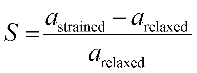
In this section, the relevant structural properties such as bond length, bond angle, interlayer distance (ILD), and lattice vectors of the optimized SnSSe bilayers are considered in different interlayer chalcogen pairing configurations, as illustrated in Fig. 4a–c. Next, these properties are compared with those of the monolayers of SnSSe, SnS2 and SnSe2 as indicated in the ESI (Fig. S1†) to assess the influence of the interlayer chalcogen pair environment on the overall structural characteristics. | ||
| Fig. 4 Schematic representation of the unit-cell of 2L-SnSSe for (a) S–S, (b) S–Se and (c) Se–Se configurations and their average electron densities of (d) 1L-SnSSe, (e) 2L-SnSSe, (S–S) (f) 2L-SnSSe (S–Se), and (g) 2L-SnSSe (Se–Se) configurations. | ||
The lattice constant of the SnSSe monolayer is 3.82 Å, which lies between the lattice constants of SnS2 (3.71 Å) and SnSe2 (3.91 Å) monolayers (Fig. S1†), and is consistent with previous theoretical reports.23,29 Similarly, in the SnSSe monolayer, the ∠S–Sn–Se bond angles assume an intermediate value (89.82°) compared to ∠S–Sn–S bond angle (89.51°) and ∠Se–Sn–Se bond angle (90.98°) in SnS2 and SnSe2 monolayers, respectively (Fig. S1†). Interestingly, in the SnSSe environment, the Sn–S (Sn–Se) bond length increases (decreases) from 2.61 Å to 2.65 Å (2.78 Å to 2.75 Å) compared to monolayer SnS2 (SnSe2) (Fig. S1†). This suggests that the Janus (SnSSe) environment notably influences the in-plane tin (Sn)–chalcogen (S/Se) atomic orbital interactions compared to natural (SnS2 and SnSe2) environments.
As indicated in Fig. 4a–c, the presence of monolayer SnSSe in a bilayer configuration introduces three distinct chalcogen pairings i.e., S–S, S–Se, and Se–Se. In the SnSSe bilayer, irrespective of chalcogen pairing, the Sn–S and Sn–Se bond lengths slightly increased from 2.65 Å to 2.66 Å and 2.75 Å to 2.76 Å, respectively, as compared to the SnSSe monolayer (Fig. S1c†). Moreover, the ∠S–Sn–Se bond angles of SnSSe decrease from 89.82° to 88.80° in S–S, 89.82° to 89.17° in Se–Se, and 89.82° to 89.18° (top monolayer), 89.82° to 89.03° (bottom monolayer) in S–Se chalcogen pairings of the bilayer SnSSe compared to the SnSSe monolayer (Fig. S1c†). This indicates that bilayer formation leads to simultaneous expansion in the in-plane direction and compression in the vertical direction in individual monolayers of SnSSe. Consequently, in each bilayer configuration, the tin (Sn)–chalcogen (S/Se) atomic orbital interactions are relatively weakened, which is expected to influence the energy band (E–k) structure of the bilayers.
Apart from the modulation of in-plane atomic orbital interactions, out-of-plane atomic orbital interactions between monolayers are another crucial factor in the bilayer environment. This can be observed from the fact that in each configuration, the interfacial chalcogen atoms exhibit a notably larger valence charge redistribution, i.e. Qtransfer_atom compared to the surface chalcogen atoms. Therefore, the atomic orbital interactions between the interlayer chalcogen atoms are expected to have a significant influence on the energy band (E–k) structure of the bilayers. In this effect, the average electron density projections in the out-of-plane direction of bilayer SnSSe at different interlayer chalcogen pair configurations are compared with isolated monolayer SnSSe, as illustrated in Fig. 4d–g.
The average electron density projections of monolayer SnSSe exhibit two peaks, where the larger and smaller peaks are consistent with the presence of Se (4s2 4p4) and S (3s2 3p4) atoms, respectively. In bilayer SnSSe, irrespective of interlayer chalcogen pair configurations, a finite average electron density is observed at the interface of the top and bottom layers, suggesting a significant atomic orbital interaction between the interlayer chalcogen atoms. However, the difference in interlayer atomic orbital interaction in different bilayers can be appreciated from the fact that ILD significantly varies from one chalcogen pair configuration to another. The trend observed in the ILD is consistent with previous reports, wherein the largest and smallest ILDs are observed in the Se–Se and S–S configurations, respectively.29 Specifically, the effective out-of-plane van der Waals (vdW) radius overlapping in S–S, S–Se, and Se–Se configurations are 1.08 Å (S vdW radius 1.89 Å), 0.90 Å (S vdW radius 1.89 Å, Se vdW radius 1.82 Å), 0.67 Å (Se vdW radius 1.82 Å), suggesting the interlayer atomic orbital interactions are distinctly different in each of the bilayers. On the other hand, in the case of S–S and Se–Se interlayer chalcogen pair configurations, a symmetric out-of-plane S–S and Se–Se p-orbital hybridization is expected, wherein S–Se interlayer chalcogen pairing should result in asymmetric out-of-plane S (3s2 3p4) and Se (4s2 4p4) p-orbital hybridizations. Such asymmetric out-of-plane atomic orbital hybridization is expected to have distinct influences on the electronic (Bloch states) states of the S–Se configuration, compared to S–S and Se–Se configurations.
Next, the S–S pairing of bilayer SnSSe, compared to the monolayer, presents a symmetric electron density distribution around a horizontal axis between the layers, with the electron density distribution of the second layer mirroring the first. Similarly, the Se–Se bilayer exhibits a symmetric distribution. In contrast, the S–Se pairing breaks the interlayer mirror symmetry in the average electron density distribution due to dissimilar chalcogen pairing. The asymmetric electronic distribution in S–Se interlayer chalcogen pair configuration suggests distinctly different out-of-plane atomic orbital interactions compared to S–S and Se–Se configurations. The asymmetric electronic distribution at the interlayer interface in the S–Se configuration results in a finite interlayer charge transfer, which is quantified from the Mulliken charge analysis. Consequently, unlike S–S and Se–Se configurations, for the S–Se configuration, a bottom-to-top layer charge transfer (Qtransfer_layer = 0.02 e− per unit-cell, i.e. 2.2 μC cm−2) is observed, which results in an intrinsic interlayer dipole moment (considering ILD = 2.81 Å) of ∼0.27 D unit-cell, i.e. 1.81 × 10¹⁴ D cm−2. The presence of such interlayer dipole moments in the S–Se configuration of bilayer SnSSe is consistent with previous theoretical reports.29,30
Thus, the factors discussed above are expected to characteristically influence the energy band (E–k) structure of S–Se bilayers compared to their S–S and Se–Se bilayer counterparts.
3.3. Electrostatic and electronic properties
The average electron density projection analysis presented in the previous section suggests the possibility of chalcogen pair configuration-dependent interlayer charge transfer in bilayer SnSSe. Consequently, in this section, the electrostatics of the bilayers are considered in terms of the average electrostatic difference potential and electron difference densities, as illustrated in Fig. 5. Next, to assess the influence of the aforementioned factors on the electronic properties of SnSSe bilayers, in this section, the energy band structures, total density of states (TDOS) profiles, individual monolayer projected density of states (PDOS), and spatial distributions of electronic states (Bloch states) at the conduction and valence band edges are analysed, and the results are shown in Fig. 6 and 7.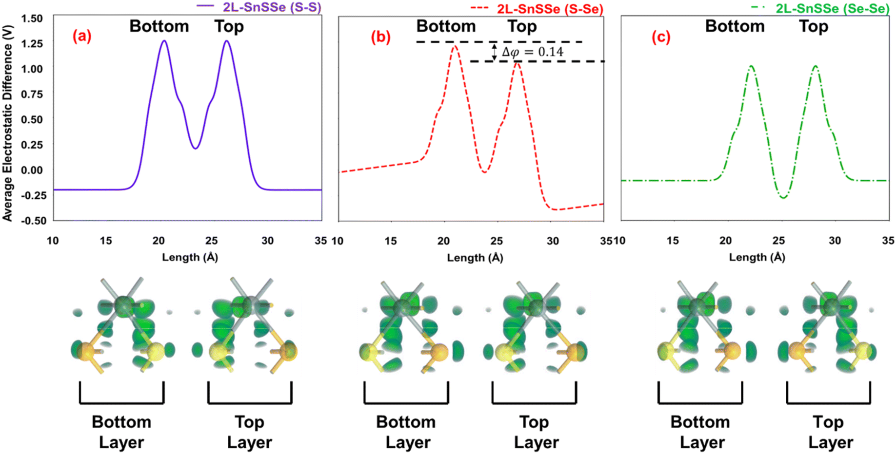 | ||
| Fig. 5 Representation of average electrostatic difference potential and electron difference density of 2L-SnSSe for (a) S–S, (b) S–Se, and (c) Se–Se configurations. | ||
 | ||
| Fig. 6 Comparative energy band and DOS profiles of 2L-SnSSe for (a) S–S, (b) S–Se, and (c) Se–Se chalcogen configurations. | ||
 | ||
| Fig. 7 Comparative band structure projections and Bloch states of 2L-SnSSe for (a) S–S, (b) S–Se, (c) Se–Se chalcogen configurations. | ||
Moreover, the average electrostatic difference potential peaks around the Sn atoms of each monolayer remain comparable in magnitude for S–S and Se–Se configurations. However, these electrostatic difference potential peaks have notably different magnitudes (Δφ = 0.14 V) in both monolayers of the S–Se configuration. In this context, an effective interlayer electric field (Eeff) is defined in this study as follows:
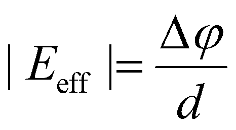 | (7) |
In eqn (7), d is the ILD between the two SnSSe layers. Therefore, it can be inferred that the interlayer charge transfer induces an electrostatic potential difference (Δφ) between the SnSSe layers, and consequently, a finite Eeff is expected in the S–Se configuration. Therefore, an Eeff of ∼0.5 V nm−1 was calculated for the S–Se configuration of bilayer SnSSe. The presence of such an interlayer electric field in the S–Se configuration of bilayer SnSSe is consistent with previous theoretical reports.30
Consequently, in this study, the energy band structures were simulated using HSE-06 (with SOC), where the calculated bandgap values of 1.49 eV (S–S), 1.47 eV (Se–Se), and 1.27 (S–Se) are consistent with previously reported HSE-06-SOC simulated bandgap values of 1.37 eV (S–S), 1.40 eV (Se–Se), and 1.26 (S–Se).34 Furthermore, similar to previous theoretical reports, each SnSSe bilayer exhibits an indirect bandgap, with the CBM located at the ‘M’ point and the ‘VBM’ at the ‘G’ point.29,34 Thus, the close agreement between the energy band structure and the bandgap values previously reported in previous studies confirms the reliability of the computational framework proposed in this study.
In general, the bands below the VBM of each bilayer show a relatively less dispersive nature, leading to larger DOS at the VBM as well as localized DOS peaks below the VBM, as shown in the TDOS profiles in Fig. 6. In contrast, a delocalized and relatively smaller DOS profile was observed above the CBM in each bilayer. Interestingly, in the S–Se configuration, the bands below the VBM showed better dispersion, resulting in reduced localized peaks in the DOS below the VBM in this case. For a more detailed analysis of the electronic properties of different bilayers, the atomic orbital projected DOS profiles were considered and are presented as ESI (Fig. S2†). PDOS analysis demonstrates that in each bilayer, the conduction band (CB) is populated by the s-orbital of the Sn atom and predominantly the in-plane px- and py-orbitals of both S and Se atoms. In contrast, the valence band (VB) of these bilayers is predominantly populated by the out-of-plane pz-orbitals of both S and Se atoms. Moreover, an effectively uniform Sn s-orbital and S and Se px/py-orbitals hybridization is observed in the CB of each bilayer. This suggests that the in-plane tin-chalcogen orbital interaction is expected to exert significant influence on the CB, whereas the out-of-plane orbital interactions of interlayer chalcogen atoms are expected to notably influence the VB of these bilayers.
A systematic inspection of Fig. 7 establishes that for S–S and Se–Se configurations, the CBM (at ‘M’ point) and the VBM (at ‘G’ point) are equally populated by the top and bottom layers. In this effect, the CBM and VBM Bloch states are spatially distributed in both SnSSe layers, consistent with the band structure analysis. Typically, in the S–S configuration, the VBM Bloch state is delocalized across the entire lattice, which is consistent with the strongest vdW radius overlapping (1.08 Å) of the interlayer S atoms. Whereas, in Se–Se configuration, the VBM Bloch states are more localized around the interfacial chalcogen atoms, which can be correlated with the weakest vdW radius overlapping (0.67 Å) in this case. Interestingly, the CBM Bloch state is localized around the interface chalcogen atoms in S–S configurations, and delocalized across the entire lattice in Se–Se configurations.
The individual monolayer projected band structure of S–Se configuration shows a stark contrast compared to that of S–S and Se–Se configurations, where a clear type-2 band alignment is observed. A similar type-2 band alignment with an intrinsic electric field was previously reported in bilayer MoSSe.33 In the S–Se configuration of a bilayer, the CBM is occupied by the bottom SnSSe layer, and the VBM is occupied by the top SnSSe layer. In agreement with the projected band structure, in the S–Se configuration, the CBM and VBM Bloch state distributions are confined in the bottom and top layers, respectively. This scenario is perfectly consistent with the interlayer charge transfer and subsequent Eeff analysis. The VBM Bloch state confinement at the top SnSSe layer and the CBM Bloch state confinement at the bottom SnSSe layer suggest that in their ground-state configurations, electrons and holes are spatially separated in different monolayers of bilayer SnSSe. Moreover, the projected band structure indicates that at CB (VB), the contribution bottom (top) SnSSe layer appears at a notably higher ∼0.36 eV (lower ∼0.29 eV) energy (offset) than the bottom (top) SnSSe layer. This suggests the stability of interlayer separated electrons and holes even at room temperature (offsets ≫ KT ∼ 0.026 eV at T = 300 K) in their respective monolayers.
The bilayer SnSSe exhibits an indirect band gap in each stacking configuration, indicating a relatively larger radiative excitonic lifetime.36,39 On the other hand, compared to S–S and Se–Se stacking configurations, the S–Se configuration shows a clear type-2 band alignment with a relatively larger band offset, suggesting thermally stable interlayer excitons. It is well established that the overlap between electron and hole wavefunctions significantly influences the oscillation strength, which is inversely proportional to the radiative excitonic lifetime.76,77 Therefore, in S–Se configuration, the localization of the CBM (electron) and VBM (hole) Bloch states (electronic wavefunction) in the alternative SnSSe monolayer reduced the electron and hole wave function overlap and should lead to a larger radiative excitonic lifetime due to the decreased oscillation strength owing to the reduced wave function overlap between spatially separated electrons and holes. A similar trend was previously observed in vdW TMD bilayers with type-2 band alignment.36,39,78
Next, in this study, the effects of biaxial strain and interlayer distance variation are systematically studied on the electronic and excitonic properties of a homogeneous bilayer of SnSSe in the S–Se stacking configuration. The biaxial strain influences both in-plane and interlayer atomic orbital interactions, wherein interlayer distance variation primarily influences the interlayer atomic orbital interactions.38,39,79 These modulations in the in-plane and interlayer atomic orbital interactions are manifested in the spread of the conduction band in energy, which can, in turn, be qualitatively correlated with the excitonic radiative lifetime following a time-energy uncertainty argument. The excitonic lifetime depends on multiple factors, and a detailed analysis of the lifetime requires extensive analytical modelling, preferably supported by experimental optical characterizations. However, these aspects are out of the scope of this study, where a simplified qualitative analysis based on the time-energy uncertainty relation and spatial separation of electron and hole wave functions can offer a reasonable assessment of excitonic radiative lifetime variations with biaxial strain and interlayer distance variation.
3.4 Influence of interlayer distance on the electronic properties of bilayer SnSSe in S–Se interlayer chalcogen pair configuration
The electronic property analysis indicates that the interlayer atomic orbital interactions of chalcogen atoms have a crucial influence on the band edge electronic states and thereby on the overall electronic properties of bilayers, which is most significant in S–Se interlayer chalcogen pair configuration owing to the type-2 band alignment in this homogeneous bilayer. However, the strength of such interlayer atomic orbital interactions can be efficiently tuned by varying the ILD between the SnSSe monolayers. Thus, in this section, the influence of ILD variations on the overall electronic properties of S–Se interlayer chalcogen pair configurations is studied, where the ILD compression and expansion are restricted up to 1.5 with respect to the equilibrium ILD of the S–Se configuration. The effects of ILD variation on the CBM energy, VBM energy, energy bandgap, energy band structure, and individual monolayer projected energy band structure are presented in plots in Fig. 8. To further analyse these aspects, the spatial distribution of band edge Bloch states and atomic orbital projected density of states were considered for increased and reduced interlayer separations in the ESI (Fig. S3†). | ||
| Fig. 8 Comparative analysis of interlayer distance variation for (a) conduction band edge energies for S–Se, (b) valence band edge energies for S–Se, (c) electronic bandgap of bilayer SnSSe, (d) band structure and monolayer projections for 1.5 Å interlayer distance reduction, and (e) band structure and monolayer projections for +1.5 Å interlayer distance expansion. | ||
 | ||
| Fig. 9 Plot of (a) CB edge offset energy and (b) VB edge offset energy variations with interlayer distance variation for S–Se configuration of the SnSSe bilayer. | ||
This analysis revealed that ILD significantly modulates the electronic and excitonic properties of the S–Se configuration of the SnSSe homogeneous bilayer, suggesting further design flexibility in terms of band alignment tailoring by tuning the ILD.
3.5 Influence of biaxial strain on the electronic properties of bilayer SnSSe in S–Se interlayer chalcogen pair configuration
This section investigates the influence of biaxial tensile (BT) and biaxial compressive (BC) strains on the electronic properties of the S–Se configuration of bilayer SnSSe. Specifically, the energy band structures, spatial distribution of band edge Bloch states, individual monolayer projection on the energy band structure, and total density of states were considered at 5% BC and BT strain, and are illustrated in Fig. 10. In this context, the Eeff, energy bandgap, primary and secondary band edge energies are considered as functions of biaxial strain variation, as illustrated in Fig. 11. | ||
| Fig. 10 Plots of (a) energy band structure, (b) Bloch states, (c) monolayer projected band structure, and (d) TDOS of bilayer SnSSe in S–Se configuration for 5% BC and 5% BT strains. | ||
 | ||
| Fig. 11 Plots of (a) interlayer effective electric field, (b) electronic band structure, (c) conduction band edge energies, (d) valence band edge energies, (e) CB edge offset energy, and (f) VB edge offset energy with varying biaxial strain in S–Se configuration of bilayer SnSSe. | ||
Biaxial compressive strain suggests that a material is subjected to tensile (outward) stress along two in-plane lattice vector directions, which strains the material, and the direction of strain is opposite to the stress. Consequently, the biaxial tensile stress will lead to biaxial compressive strain, and following a similar argument, biaxial compressive stress will lead to biaxial tensile strain.81 Specifically, under such compressive strain, the material undergoes elongation in the in-plane lattice directions that increases the bond lengths, as shown in Fig. S4.† Conversely, biaxial tensile strain contracts the material in the in-plane lattice directions, causing bond length reduction, as shown in Fig. S4.† Following this notion in this paper, the induced strain and applied stress are simultaneously mentioned in the “strain-type (corresponding stress type)” format.
At the same time, from the PDOS and conduction band spread analysis (Fig. S5, S6 and S7b†), it can be observed that the 5% BT strain delocalizes the CB electronic states in energy owing to the stronger in-plane atomic orbital interactions, which leads to an increase in energy uncertainty in CB. However, the type-2 band alignment was preserved under a 5% BT strain. The application of strain simultaneously modifies both in-plane and interlayer atomic orbital interactions, where increasing BT (BC) strain reduces (enhances) interlayer atomic orbital interaction and increases (decreases) in-plane atomic orbital interaction. Consequently, increasing interlayer atomic orbital interaction with BC strain annihilates the type-2 band alignment. Moreover, increasing BC strain marginally influences the localization of CB in energy, thereby affecting their energy-time uncertainty. Interestingly, the increasing BT (BC) strain increases (decreases) the ILD and thereby the separation of electron and hole wave functions, which is expected to reduce (enhance) the oscillation strength and thereby improve (degrade) the excitation radiative lifetime. Therefore, combining both spatial separation electron–hole wave function and energy-time uncertainty argument, it can be surmised that the increase in BC and BT strain involves competing influences on the radiative lifetime of excitons and is expected to degrade the overall radiative lifetime of excitons compared to the relaxed configuration. However, owing to the annihilation of type-2 band alignment, this effect is expected to be more prominent in larger BC strains. A similar trend has been experimentally observed in a MoS2/WSe2 heterostructure,38 where the radiative lifetime of interlayer excitons is reduced after applying both uniaxial tensile and compressive strain.
Fig. 11c shows that the CB edge energy at the ‘M’ point (‘G’ point) decreases (increases) with increasing BT and increases (reduces) with increasing BC. This further leads to a shift in the CBM from the ‘M’ point to the ‘G’ point at a higher BC strain. Similarly, Fig. 11d indicates that the VB edge energy at the ‘G’ point increases with increasing BT and reduces with increasing BC. The VBM shifts from the ‘G’ point to an intermediate point between the ‘K’ and ‘G’ point at a higher BC strain, and the VB edge energy between the ‘K’ to ‘G’ point keeps increasing with BC strain.
Next, for the type-2 band alignment, the CB and VB edge separation (offset) between the top and bottom SnSSe layers is considered as a function of biaxial strain, as illustrated in Fig. 11e and f. The type-2 band alignment is annihilated at a larger BC strain, and therefore, the band edge offset is not considered from that point onwards. The results indicate that both the CB and VB offsets are increasing (decreasing) with increasing BT (BC) strain. This suggests that the BT strain is a highly promising material engineering technique for increasing the band edge offset while retaining type-2 band alignment in the S–Se configuration. This indicates that stable interlayer excitons can be realized through suitable optical excitation at room temperature (offsets ≫ KT ∼ 0.026 eV at T = 300 K) in a tensile-strained S–Se configuration of the SnSSe bilayer.
3.6. Comparative analysis
The key findings of this study are compared with previously reported theoretical findings on SnSSe and Janus TMD bilayers. Previous theoretical reports on SnSSe bilayers also reported a notably small energy bandgap in the S–Se configuration compared to S–S and Se–Se configurations.29,30 Moreover, a non-zero interlayer dipole moment and interlayer electric field were previously reported in the S–Se configuration of the SnSSe bilayer, which is consistent with the findings of this study.29,30 On the other hand, a previous theoretical study on Janus WSSe bilayer shows comparable interlayer interaction energies at different interlayer chalcogen pair configurations,28 consistent with that of the SnSSe bilayers reported in this study. Next, as observed for relaxed SnSSe bilayers in this study, both Janus MoSSe41 and WSSe28 bilayers show the lowest bandgap at S–Se interlayer chalcogen pairs at different interlayer stacking orientations, which is consistent with the findings of this study. Moreover, similar to the S–Se configuration of the SnSSe bilayer reported in this study, the asymmetrical interlayer chalcogen pairing in MoSSe leads to a finite interlayer charge transfer41 and subsequent interlayer dipole moment42 and electric field.41 On the other hand, for MoSeTe and WSeTe bilayers in asymmetrical interlayer chalcogen pairing with in AA interlayer stacking, the decreasing ILD shows a drastic reduction of energy bandgaps and eventually semiconducting to metallic transformations, wherein a small reduction in energy bandgap can be observed with increasing ILD.43 These trends are in good agreement with the qualitative trend of bandgap variations, with the ILD variation study of this work. Interestingly, in the S–Se configuration of the Janus WSSe bilayer, the application of both BC and BT strain reduces the energy bandgap, as also observed in this study for the S–Se configuration of the SnSSe bilayer.28 Finally, the previously reported interlayer electric fields and dipole moment values for different Janus TMD bilayers in their asymmetric interlayer chalcogen pairing configurations are compared with the findings of this study in Table 3.Therefore, the comparative analysis emphatically suggests that the asymmetric interfacial chalcogen pairing in Janus TMD bilayers can induce finite interlayer charge transfer, interlayer dipole moment and a built-in interlayer electric field. The presence of an interlayer electric field is expected to induce a type-2 band alignment with interlayer excitons and simultaneously a bandgap reduction in Janus TMD bilayers with asymmetric interfacial chalcogen pairing. Moreover, the S–Se stacking configuration of Janus SnSSe exhibits a comparable interlayer dipole moment and intrinsic interlayer electric field to those previously observed in MoSSe.
Finally, to date, a number of Janus monolayer TMDs, including SnSSe, have been successfully synthesized using CVD using selenization or sulfurization of the top chalcogen layer,12,13 selective epitaxy atomic replacement,14 hot injection of Se precursor and S precursor solutions into the Sn precursor15 and plasma-driven selenization.16 However, the controlled synthesis of few-layered Janus TMDs using precise interfacial chalcogen combinations is a significant challenge. To the best of the authors’ knowledge, to date, the closest attempt in this direction has reported the heterostructure of MoSSe with MoS2 with S–Se and S–S interfacial chalcogen combinations.82 Specifically, monolayer MoSSe is prepared by selenization of CVD-synthesized monolayer MoS2, followed by its transfer onto the as-grown monolayer MoS2 using poly-methyl methacrylate (PMMA) to form either S–S or Se–S interfacial chalcogen combinations at the hetero-interfaces.82 Therefore, adapting these synthesis strategies for bilayer SnSSe, particularly to realize well-defined S–Se interlayer configurations, is likely to require an integrated approach combining vertical layer-by-layer transfer with plasma-assisted chalcogen-substitution techniques. These methods require precise control over stacking order and interfacial cleanliness. Specifically, achieving selective alignment of S and Se atoms across layers without significant lattice distortion remains a formidable challenge. Nevertheless, overcoming these obstacles can pave the way for high-performance optoelectronic devices based on SnSSe bilayers.
4. Conclusion
In this study, the effects of different interfacial chalcogen pair configurations on the structural and electronic properties of Janus SnSSe bilayers were extensively investigated, emphasizing the interlayer energy band alignment. This is followed by a detailed study of interlayer band alignments with respect to interlayer distance and biaxial strain variations. The results indicate that three distinct interlayer chalcogen pair configurations, i.e. S–S, S–Se, Se–Se, can be realized in bilayer SnSSe, where each configuration is energetically and dynamically stable and is equally likely to form. The breaking of out-of-plane mirror symmetry in the S–Se configuration results in unique properties, including finite interlayer transferred charge density (∼2.2 μC cm−2), finite interlayer dipole moment density (∼1.81 × 10¹⁴ D cm−2), finite effective interlayer electric field (∼0.5 V nm−1), reduced energy bandgap (∼14%–15% Eg reduction), and type-2 band alignment compared to other two interlayer chalcogen pair configurations. Moreover, S–Se configuration demonstrates clear interlayer separations between the CBM and VBM Bloch state with CB offset ∼0.36 eV and VB offset ∼0.29 eV in its type-2 band alignment, suggesting the unique possibility of realizing interlayer excitons in a homogeneous bilayer. The results further suggest that the variation in the interlayer separations and applied biaxial strain can be used to effectively tune the electronic properties of the S–Se configuration of the SnSSe bilayer. Typically, both smaller ILDs and larger BC strains can annihilate the type-2 band alignment while causing a drastic reduction in Eg (∼43% at 5% BC strain from 2% BC strain) in the S–Se configuration. In contrast, in S–Se configuration, increasing ILD slightly reduces the Eg (∼8% with 1.5 Å increase in ILD), retaining the type-2 band alignment, with a slight increase in VB offset (∼6% with 1.5 Å increase in ILD) and comparable CB offset, while expecting to improve the interlayer exciton radiative lifetime owing to reducing electron–hole wave function overlap. However, increasing the BT strain retains the type-2 band alignment, and at the same time, notably reduces the Eg (∼42% at 5% BT strain from relaxed configuration) and increases the CB/VB offset (∼33% increase in CB and 19% increase in VB at 5% BT strain from relaxed configuration), while expecting to slightly degrade the interlayer exciton radiative lifetime in S–Se configuration owing to increasing conduction band spread in energy. In summary, this study demonstrated that dissimilar chalcogen pairing in the Janus SnSSe bilayer is a potential homogeneous 2D material system for realizing type-2 band alignment, which can be further efficiently tuned by applying BT strain and increasing ILD. The generation of interlayer excitons in such strain-engineered S–Se configuration of SnSSe bilayers can lead to the realization of tuneable electron–hole separation in real and reciprocal spaces. The presence of interlayer exciton in S–Se configuration of SnSSe bilayers and their tunability with increasing ILD and BT strain can offer significant advantages for electronic and optoelectronic applications, including exciton-based transistors, ultra-low threshold lasers, excitonic transistors, ultra-sensitive broadband photodetectors, and tuneable LED designs. Moreover, the realization and manipulation of interlayer excitons are expected to play a transformative role in valleytronics for low-power information processing, including energy-efficient data manipulation and storage.Author contributions
Naresh Bahadursha: visualization, validation, software, methodology, writing – original draft, preparation, investigation, and data curation. Chanda Bhavitha Sri: validation, software, methodology, and data curation. Kuna Krishna Ruthvik: validation, software, methodology, and data curation. Swastik Bhattacharya: writing – review and editing, investigation, and formal analysis. Sayan Kanungo: writing – review and editing, writing – original draft, validation, supervision, investigation, formal analysis, and conceptualization.Data availability
The data supporting this article have been included as part of the ESI.†The code for ab initio DFT simulations can be found at https://www.synopsys.com/manufacturing/quantumatk.html and is described in J. Phys.:Condens. Matter (APS), vol. 32, p. 015901 (2020). The code used in this study was the QuantumATK version V-2023.12.
Conflicts of interest
The authors declare that they have no known competing financial interests or personal relationships that could have appeared to influence the work reported in this paper.Acknowledgements
The computational research for this work was carried out in the Computational Nanomaterials and Nanodevices Research Lab (CNNRL) of the EEE Department, BITS-Pilani, Hyderabad Campus. The authors acknowledge Prof. Sk. Masum Nawaz of EEE Department, BITS-Pilani, Hyderabad Campus for his support during this research.References
- Z. Lin, A. McCreary, N. Briggs, S. Subramanian, K. Zhang, Y. Sun, X. Li, N. J. Borys, H. Yuan, S. K. Fullerton-Shirey and A. Chernikov, 2D materials advances: from large scale synthesis and controlled heterostructures to improved characterization techniques, defects and applications, 2D Mater., 2016, 3(4), 042001, DOI:10.1088/2053-1583/3/4/042001
.
- T. Dutta, N. Yadav, Y. Wu, G. J. Cheng, X. Liang, S. Ramakrishna, A. Sbai, R. Gupta, A. Mondal, Z. Hongyu and A. Yadav, Electronic properties of 2D materials and their junctions, Nano Materials Science, 2024, 6(1), 1–23, DOI:10.1016/j.nanoms.2023.05.003
- P. V. Pham, S. C. Bodepudi, K. Shehzad, Y. Liu, Y. Xu, B. Yu and X. Duan, 2D heterostructures for ubiquitous electronics and optoelectronics: principles, opportunities, and challenges, Chem. Rev., 2022, 122(6), 6514–6613, DOI:10.1021/acs.chemrev.1c00735
- M. H. Lee and W. Wu, 2D materials for wearable energy harvesting, Adv. Mater. Technol., 2022, 7(9), 2101623, DOI:10.1002/admt.202101623
- T. Vincent, J. Liang, S. Singh, E. G. Castanon, X. Zhang, A. McCreary, D. Jariwala, O. Kazakova and Z. Y. Al Balushi, Opportunities in electrically tunable 2D materials beyond graphene: Recent progress and future outlook, Appl. Phys. Rev., 2021, 8(4), 041320, DOI:10.1063/5.0051394
- M. C. Lemme, D. Akinwande, C. Huyghebaert and C. Stampfer, 2D materials for future heterogeneous electronics, Nat. Commun., 2022, 13(1), 1392, DOI:10.1038/s41467-022-29001-4
- L. Du, T. Hasan, A. Castellanos-Gomez, G. B. Liu, Y. Yao, C. N. Lau and Z. Sun, Engineering symmetry breaking in 2D layered materials, Nat. Rev. Phys., 2021, 3(3), 193–206, DOI:10.1038/s42254-020-00276-0
- S. Barraza-Lopez, F. Xia, W. Zhu and H. Wang, Beyond graphene: low-symmetry and anisotropic 2D materials, J. Appl. Phys., 2020,(14), 128, DOI:10.1063/5.0030751
- X. Tang and L. Kou, 2D Janus transition metal dichalcogenides: Properties and applications, Phys. Status Solidi B, 2022, 259(4), 2100562, DOI:10.1002/pssb.202100562
- L. Zhang, Y. Xia, X. Li, L. Li, X. Fu, J. Cheng and R. Pan, Janus two-dimensional transition metal dichalcogenides, J. Appl. Phys., 2022,(23), 131, DOI:10.1063/5.0095203
- W. J. Yin, H. J. Tan, P. J. Ding, B. Wen, X. B. Li, G. Teobaldi and L. M. Liu, Recent advances in low-dimensional Janus materials: theoretical and simulation perspectives, Mater. Adv., 2021, 2(23), 7543–7558, 10.1039/D1MA00660F
- A. Y. Lu, H. Zhu, J. Xiao, C. P. Chuu, Y. Han, M. H. Chiu, C. C. Cheng, C. W. Yang, K. H. Wei, Y. Yang and Y. Wang, Janus monolayers of transition metal dichalcogenides, Nat. Nanotechnol., 2017, 12(8), 744–749, DOI:10.1038/nnano.2017.100
- J. Zhang, S. Jia, I. Kholmanov, L. Dong, D. Er, W. Chen, H. Guo, Z. Jin, V. B. Shenoy, L. Shi and J. Lou, Janus monolayer transition-metal dichalcogenides, ACS Nano, 2017, 11(8), 8192–8198, DOI:10.1021/acsnano.7b03186
- D. B. Trivedi, G. Turgut, Y. Qin, M. Y. Sayyad, D. Hajra, M. Howell, L. Liu, S. Yang, N. H. Patoary, H. Li and M. M. Petrić, Room–temperature synthesis of 2D Janus crystals and their heterostructures, Adv. Mater., 2020, 32(50), 2006320, DOI:10.1002/adma.202006320
- K. Mukai and K. Nakayama, Study on chemical synthesis of SnSSe nanosheets and nanocrystals, Jpn. J. Appl. Phys., 2022, 61(SC), SC1012, DOI:10.35848/1347-4065/ac3d0d
- S. M. He, J. Y. Zhuang, C. F. Chen, R. K. Liao, S. T. Lo, Y. F. Lin and C. Y. Su, Plasma–Driven Selenization for Electrical Property Enhancement in Janus 2D Materials, Small Methods, 2024, 8(10), 2400150, DOI:10.1002/smtd.202400150
- E. M. Flores, V. J. R. Rivera, E. J. S. Sacari, J. R. Sambrano, M. L. Moreira and M. J. Piotrowski, Biaxial strain effects on electronic, transport, and thermoelectric properties of SnX2 (X = Se, Te) and Janus SnSeTe 1T-monolayers, Mater. Today Commun., 2024, 39, 108830, DOI:10.1016/j.mtcomm.2024.108830
- X. Zhang, Y. Cui, L. Sun, M. Li, J. Du and Y. Huang, Stabilities, and electronic and piezoelectric properties of two-dimensional tin dichalcogenide derived Janus monolayers, J. Mater. Chem. C, 2019, 7(42), 13203–13210, 10.1039/C9TC04461B
- B. D. Bhat, Rashba spin-splitting in Janus SnXY/WXY (X, Y = S, Se, Te; X≠ Y) heterostructures, J. Phys.: Condens. Matter, 2023, 35(43), 435301, DOI:10.1088/1361-648X/ace8e4
- S. D. Guo, X. S. Guo, R. Y. Han and Y. Deng, Predicted Janus SnSSe monolayer: a comprehensive first-principles study, Phys. Chem. Chem. Phys., 2019, 21(44), 24620–24628, 10.1039/C9CP04590B
- S. Bai, S. Tang, M. Wu, D. Luo, J. Zhang, D. Wan and S. Yang, Unravelling the thermoelectric properties and suppression of bipolar effect under strain engineering for the asymmetric Janus SnSSe and PbSSe monolayers, Appl. Surf. Sci., 2022, 599, 153962, DOI:10.1016/j.apsusc.2022.153962
- L. Huang, D. Lu, W. Zeng and Q. Zhou, Favorable adsorption and detection properties of metal oxides (NiO, Ag 2 O) modified Janus SnSSe monolayer towards SF 6 decomposition gases in a gas-insulated equipment, IEEE Sens. J., 2024, 24(22), 37042–37052, DOI:10.1109/JSEN.2024.3471830
- H. T. Nguyen, V. V. Tuan, C. V. Nguyen, H. V. Phuc, H. D. Tong, S. T. Nguyen and N. N. Hieu, Electronic and optical properties of a Janus SnSSe monolayer: effects of strain and electric field, Phys. Chem. Chem. Phys., 2020, 22(20), 11637–11643, 10.1039/D0CP01860K
- B. Xu, C. Qian, Z. Wang, J. Zhang, S. Ma, Y. Wang and L. Yi, First-principles study of magnetic properties and electronic structure of 3d transition-metal atom–adsorbed SnSSe monolayers, Phys. Chem. Chem. Phys., 2024, 26(5), 4231–4239, 10.1039/D3CP04740G
- T. V. Vu, V. H. Chu, J. Guerrero-Sanchez and D. M. Hoat, Regulating the Electronic and Magnetic Properties of a SnSSe Janus Monolayer toward Optoelectronic and Spintronic Applications, ACS Appl. Electron. Mater., 2024, 6(5), 3647–3656, DOI:10.1021/acsaelm.4c00341
- N. Bahadursha, A. Tiwari, S. Chakraborty and S. Kanungo, Theoretical investigation of the structural and electronic properties of bilayer van der Waals heterostructure of Janus molybdenum di-chalcogenides–Effects of interlayer chalcogen pairing, Mater. Chem. Phys., 2023, 297, 127375, DOI:10.1016/j.matchemphys.2023.127375
- Y. Gao and S. Okada, Energetics and electronic structure of bilayer Janus WSSe, Appl. Phys. Express, 2023, 16(7), 075004, DOI:10.35848/1882-0786/ace33d
- J. Guo, C. Ke, Y. Wu and J. Kang, Strain engineering on the electronic and optical properties of WSSe bilayer, Nanoscale Res. Lett., 2020, 15, 1–9, DOI:10.1186/s11671-020-03330-z
- P. Wang, Y. Zong, H. Liu, H. Wen, H. X. Deng, Z. Wei, H. B. Wu and J. B. Xia, Quasiparticle band structure and optical properties of the Janus monolayer and bilayer SnSSe, J. Phys. Chem. C, 2020, 124(43), 23832–23838, DOI:10.1021/acs.jpcc.0c06186
- S. Bai, Y. Ma, M. Wu, J. Zhang, D. Luo, D. Wan and S. Tang, Unravelling the regulating role of stacking pattern on the tunable dipole, mechanical behavior and carrier mobility for asymmetric Janus SnSSe bilayer, Mater. Today Commun., 2022, 33, 104191, DOI:10.1016/j.mtcomm.2022.104191
- C. Shang, B. Xu, X. Lei, S. Yu, D. Chen, M. Wu, B. Sun, G. Liu and C. Ouyang, Bandgap tuning in MoSSe bilayers: synergistic effects of dipole moment and interlayer distance, Phys. Chem. Chem. Phys., 2018, 20(32), 20919–20926, 10.1039/C8CP04208J
- W. Zhou, J. Chen, Z. Yang, J. Liu and F. Ouyang, Geometry and electronic structure of monolayer, bilayer, and multilayer Janus WSSe, Phys. Rev. B, 2019, 99(7), 075160, DOI:10.1103/PhysRevB.99.075160
- C. Long, Y. Dai, Z. R. Gong and H. Jin, Robust type-II band alignment in Janus-MoSSe bilayer with extremely long carrier lifetime induced by the intrinsic electric field, Phys. Rev. B, 2019, 99(11), 115316, DOI:10.1103/PhysRevB.99.115316
- S. Bai, M. Wu, J. Zhang, D. Luo, D. Wan, X. Li and S. Tang, Stacking pattern induced high ZTs in monolayer SnSSe and bilayer SnXY (X/Y = S, Se) materials with strong anharmonic phonon scattering, Chem. Eng. J., 2023, 455, 140832, DOI:10.1016/j.cej.2022.140832
- Y. Luo, H. Cao, M. Li, H. Yuan and H. Liu, Tuning the lattice thermal conductivity of Janus SnSSe by interlayer twisting: a machine-learning-based study, New J. Phys., 2024, 26(4), 043013, DOI:10.1088/1367-2630/ad3c66
- K. Q. Lin, A roadmap for interlayer excitons, Light: Sci. Appl., 2021, 10, 99, DOI:10.1038/s41377-021-00544-3
- P. Rivera, H. Yu, K. L. Seyler, N. P. Wilson, W. Yao and X. Xu, Interlayer valley excitons in heterobilayers of transition metal dichalcogenides, Nat. Nanotechnol., 2018, 13(11), 1004–1015, DOI:10.1038/s41565-018-0193-0
- C. Cho, J. Wong, A. Taqieddin, S. Biswas, N. R. Aluru, S. Nam and H. A. Atwater, Highly strain-tunable interlayer excitons in MoS2/WSe2 heterobilayers, Nano Lett., 2021, 21(9), 3956–3964, DOI:10.1021/acs.nanolett.1c00724
- Z. Bai, H. Zhang, J. He, D. He, J. Wang, W. Wu and Y. Zhang,
et al., Ultrafast Decay of Interlayer Exciton in WS2/MoSe2 Heterostructure Under Pressure, Adv. Electron. Mater., 2025, 11(2), 2400333, DOI:10.1002/aelm.202400333
- J. Xia, J. Yan, Z. Wang, Y. He, Y. Gong, W. Chen, T. C. Sum, Z. Liu, P. M. Ajayan and Z. Shen, Strong coupling and pressure engineering in WSe2−MoSe2 heterobilayers, Nat. Phys., 2021, 17(1), 92–98, DOI:10.1038/s41567-020-1005-7
- L. Zhong, X. Li, Y. Pu, M. Wang, C. Zhan and X. Xiao, Tunable Li-ion diffusion properties in MoSSe bilayer anodes by strain gradient, Phys. Chem. Chem. Phys., 2024, 26(2), 1030–1038, 10.1039/D3CP04650H
- W.-J. Yin, B. Wen, G.-Z. Nie, X.-L. Wei and L.-M. Liu, Tunable dipole and carrier mobility for a few layer Janus MoSSe structure, J. Mater. Chem. C, 2018, 6(7), 1693–1700, 10.1039/C7TC05225A
- A. Rezavand and N. Ghobadi, Tuning the Rashba spin splitting in Janus MoSeTe and WSeTe van der Waals heterostructures by vertical strain, J. Magn. Magn. Mater., 2022, 544, 168721, DOI:10.1016/j.jmmm.2021.168721
- J. Guo, C. Ke, Y. Wu and J. Kang, Strain engineering on the electronic and optical properties of WSSe bilayer, Nanoscale Res. Lett., 2020, 15, 1–9, DOI:10.1186/s11671-020-03330-z
- QuantumWise [Online]. Available: https://quantumwise.com/ (n.d.).
- Y. Liu, B. W. Tang, B. Wen, X. B. Li, D. F. Zou, Y. F. Chai, Y. Xu, X. L. Wei and W. J. Yin, Non-metal atom modified SnS2 sheet for CO2 photoreduction with significant activity and selectivity improvements: A first-principles study, Appl. Surf. Sci., 2022, 584, 152618, DOI:10.1016/j.apsusc.2022.152618
- A. Rahman, H. J. Kim, M. Noor-A-Alam and Y. H. Shin, A theoretical study on tuning band gaps of monolayer and bilayer SnS2 and SnSe2 under external stimuli, Curr. Appl. Phys., 2019, 19(6), 709–714, DOI:10.1016/j.cap.2019.03.008
- Y. Huang, C. Ling, Z. Fang and S. Wang, Width-and edge-dependent magnetic properties, electronic structures, and stability of SnSe2 nanoribbons, Phys. E, 2014, 59, 102–106, DOI:10.1016/j.physe.2014.01.003
- G. Li, G. Ding and G. Gao, Thermoelectric properties of SnSe2 monolayer, J. Phys.: Condens. Matter, 2016, 29(1), 015001, DOI:10.1088/0953-8984/29/1/015001
- T. M. Henderson, J. Paier and G. E. Scuseria, Accurate treatment of solids with the HSE screened hybrid, Phys. Status Solidi B, 2011, 248(4), 767–774, DOI:10.1002/pssb.201046303
- M. Alam, H. S. Waheed, H. Ullah, M. W. Iqbal, Y. H. Shin, M. J. I. Khan, H. I. Elsaeedy and R. Neffati, Optoelectronics properties of Janus SnSSe monolayer for solar cells applications, Phys. B, 2022, 625, 413487, DOI:10.1016/j.physb.2021.413487
- H. G. Abbas, J. R. Hahn and H. S. Kang, Non-Janus WSSe/MoSSe heterobilayer and its photocatalytic band offset, J. Phys. Chem. C, 2019, 124(6), 3812–3819, DOI:10.1021/acs.jpcc.9b08255
- V. Van Thanh, N. D. Van, R. Saito and N. T. Hung, First-principles study of mechanical, electronic and optical properties of Janus structure in transition metal dichalcogenides, Appl. Surf. Sci., 2020, 526, 146730, DOI:10.1016/j.apsusc.2020.146730
- X. Ma, X. Yong, C.-c. Jian and J. Zhang, Transition metal-functionalized Janus MoSSe monolayer: a magnetic and efficient single-atom photocatalyst for water-splitting applications, J. Phys. Chem. C, 2019, 123(30), 18347–18354, DOI:10.1021/acs.jpcc.9b03003
- H. Mehdipour and P. Kratzer, Structural defects in a Janus MoSSe monolayer: A density functional theory study, Phys. Rev. B, 2022, 106(23), 235414, DOI:10.1103/PhysRevB.106.235414
- A. Togo, First-principles phonon calculations with phonopy and phono3py, J. Phys. Soc. Jpn., 2023, 92(1), 012001, DOI:10.7566/JPSJ.92.012001
- N. Bahadursha, J. Palepu, A. Tiwari, S. Chakraborty and S. Kanungo, Energy band engineering in GaS/InS and GaSe/InS van der Waals bilayers by interlayer stacking design and applied vertical electric field-An ab initio theoretical calculation based approach, Mater. Sci. Semicond. Process., 2024, 180, 108538, DOI:10.1016/j.mssp.2024.108538
- G. Qiu, H. Zhang, Y. Liu and C. Xia, Strain effect on the electronic properties of Ce-doped SnS2 monolayer, Phys. B, 2018, 547, 1–5, DOI:10.1016/j.physb.2018.07.032
- C. Jin, X. Tang, X. Tan, S. C. Smith, Y. Dai and L. Kou, A Janus MoSSe monolayer: a superior and strain-sensitive gas sensing material, J. Mater. Chem. A, 2019, 7(3), 1099–1106, 10.1039/C8TA08407F
- R. Frisenda, M. Drüppel, R. Schmidt, S. M. de Vasconcellos, D. P. de Lara, R. Bratschitsch, M. Rohlfing and A. Castellanos-Gomez, Biaxial strain tuning of the optical properties of single-layer transition metal dichalcogenides, npj 2D Mater. Appl., 2017, 1, 10, DOI:10.1038/s41699-017-0013-7
- D. Lloyd, X. Liu, J. W. Christopher, L. Cantley, A. Wadehra, B. L. Kim, B. B. Goldberg, A. K. Swan and J. S. Bunch, Band gap engineering with ultralarge biaxial strains in suspended monolayer MoS2, Nano Lett., 2016, 16(9), 5836–5841, DOI:10.1021/acs.nanolett.6b02615
- H. J. Conley, B. Wang, J. I. Ziegler, R. F. Haglund Jr., S. T. Pantelides and K. I. Bolotin, Bandgap engineering of strained monolayer and bilayer MoS2, Nano Lett., 2013, 13(8), 3626–3630, DOI:10.1021/nl4014748
- J.-U. Lee, S. Woo, J. Park, H. C. Park, Y.-W. Son and H. Cheong, Strain-shear coupling in bilayer MoS2, Nat. Commun., 2017, 8(1), 1370, DOI:10.1038/s41467-017-01487-3
- N. Tang, C. Du, Q. Wang and H. Xu, Strain engineering in bilayer WSe2 over a large strain range, Microelectron. Eng., 2020, 223, 111202, DOI:10.1016/j.mee.2019.111202
- K. Liu, L. Zhang, T. Cao, C. Jin, D. Qiu, Q. Zhou, A. Zettl, P. Yang, S. G. Louie and F. Wang, Evolution of interlayer coupling in twisted molybdenum disulfide bilayers, Nat. Commun., 2014, 5(1), 4966, DOI:10.1038/ncomms5966
- J. Palepu, P. P. Anand, P. Parshi, V. Jain, A. Tiwari, S. Bhattacharya, S. Chakraborty and S. Kanungo, Comparative analysis of strain engineering on the electronic properties of homogenous and heterostructure bilayers of MoX2 (X = S, Se, Te), Micro Nanostruct., 2022, 168, 207334, DOI:10.1016/j.micrna.2022.207334
- J. Palepu, A. Tiwari, P. Sahatiya, S. Kundu and S. Kanungo, Effects of artificial stacking configurations and biaxial strain on the structural, electronic and transport properties of bilayer GaSe-A first principle study, Mater. Sci. Semicond. Process., 2022, 137, 106236, DOI:10.1016/j.mssp.2021.106236
- W. Zhou and N. Umezawa, Insight into the band structure engineering of single-layer SnS 2 with in-plane biaxial strain, Phys. Chem. Chem. Phys., 2016, 18(11), 7860–7865, 10.1039/C6CP00039H
- L. H. Qu, J. Yu, Y. L. Mu, X. L. Fu, C. G. Zhong, Y. Min, P. X. Zhou, J. M. Zhang, Y. Q. Zou and T. S. Lu, Strain tunable structural, mechanical and electronic properties of monolayer tin dioxides and dichalcogenides SnX2 (XO, S, Se, Te), Mater. Res. Bull., 2019, 119, 110533, DOI:10.1016/j.materresbull.2019.110533
- N. D. Hien, N. Q. Cuong, L. M. Bui, P. C. Dinh, C. V. Nguyen, H. V. Phuc, N. V. Hieu, H. R. Jappor, L. T. Phuong, B. D. Hoi and L. C. Nhan, First principles study of single-layer SnSe2 under biaxial strain and electric field: Modulation of electronic properties, Physica E., 2019, 111, 201–205, DOI:10.1016/j.physe.2019.03.025
- O. V. Gritsenko, Ł.M Mentel and E. J. Baerends, On the errors of local density (LDA) and generalized gradient (GGA) approximations to the Kohn-Sham potential and orbital energies, J. Chem. Phys., 2016, 144(20), 204114, DOI:10.1063/1.4950877
- P. Borlido, J. Schmidt, A. W. Huran, F. Tran, M. A. L. Marques and S. Botti, Exchange-correlation functionals for band gaps of solids: benchmark, reparametrization and machine learning, npj Comput. Mater., 2020, 6(1), 1–17, DOI:10.1038/s41524-020-00360-0
- J. Heyd, G. E. Scuseria and M. Ernzerhof, Hybrid functionals based on a screened Coulomb potential, J. Chem. Phys., 2003, 118(18), 8207–8215, DOI:10.1063/1.2204597
- J. P. Perdew, M. Ernzerhof and K. Burke, Rationale for mixing exact exchange with density functional approximations, J. Chem. Phys., 1996, 105(22), 9982–9985, DOI:10.1063/1.472933
- R. S. Mulliken, Electronic population analysis on LCAO–MO molecular wave functions, J. Chem. Phys., 1955, 23(10), 1833–1840, DOI:10.1063/1.1740588
- G.W'T. Hooft, W. A. J. A. Van der Poel, L. W. Molenkamp and C. T. Foxon, Giant oscillator strength of free excitons in GaAs, Phys. Rev. B: Condens. Matter Mater. Phys., 1987, 35(15), 8281, DOI:10.1103/PhysRevB.35.8281
-
T. Arai and K. Matsuishi, Small Particles and Clusters, Optical Properties of, 2005, pp. 388–394. DOI:10.1016/B0-12-369401-9/00600-8
- Y. Jiang, S. Chen, W. Zheng, B. Zheng and A. Pan, Interlayer exciton formation, relaxation, and transport in TMD van der Waals heterostructures, Light: Sci. Appl., 2021, 10(1), 72, DOI:10.1038/s41377-021-00500-1
- Y.-C. Hsieh, Z.-Y. Lin, S.-J. Fung, W.-S. Lu, S.-C. Ho, S.-P. Hong and S.-Z. Ho,
et al., Engineering the strain and interlayer excitons of 2D materials via lithographically engraved hexagonal boron nitride, Nano Lett., 2023, 23(15), 7244–7251, DOI:10.1021/acs.nanolett.3c01208
- Z. Hongzhi, Y. Zhao, W. Tao, Y. Li, Q. Zhou and H. Zhu, Controlling exciton and valley dynamics in two-dimensional heterostructures with atomically precise interlayer proximity, ACS Nano, 2020, 14(4), 4618–4625, DOI:10.1021/acsnano.0c00218
- A. Michail, J. A. Yang, K. Filintoglou, N. Balakeras, C. A. Nattoo, C. S. Bailey, A. Daus, J. Parthenios, E. Pop and K. Papagelis, Biaxial Strain Transfer in Monolayer MoS2 and WSe2 Transistor Structures, ACS Appl. Mater. Interfaces, 2024, 16(37), 49602–49611, DOI:10.1021/acsami.4c07216
- K. Zhang, Y. Guo, D. T. Larson, Z. Zhu, S. Fang, E. Kaxiras, J. Kong and S. Huang, Spectroscopic signatures of interlayer coupling in Janus MoSSe/MoS2 heterostructures, ACS Nano, 2021, 15(9), 14394–14403, DOI:10.1021/acsnano.1c03779
Footnote |
| † Electronic supplementary information (ESI) available. See DOI: https://doi.org/10.1039/d5nr00552c |
| This journal is © The Royal Society of Chemistry 2025 |