
 Open Access Article
 This Open Access Article is licensed under a Creative Commons Attribution-Non Commercial 3.0 Unported Licence
Grain size engineering via a Hf0.5Zr0.5O2 seed layer for FeFET memory and synaptic devices†
Junhyeok
Park
a,
Chulwon
Chung
b,
Boncheol
Ku
a,
Seunghyeon
Yun
a,
Kyungsoo
Park
a and
Changhwan
Choi
 *a
*a
aDivision of Materials Science and Engineering, Hanyang University, Korea. E-mail: cchoi@hanyang.ac.kr
bDepartment of Energy Engineering, Hanyang University, Korea
First published on 14th March 2025
Abstract
This study demonstrates the use of a top-gate ferroelectric field effect transistor (FeFET) with the replacement electrode solid phase epitaxy (SPE) method and high deposition temperature during atomic layer deposition (ALD). By employing these engineering techniques, the average grain size was successfully reduced, and the formation of the non-ferroelectric monoclinic phase (m-phase) was effectively inhibited. In terms of ferroelectric properties, both the remanent polarization (2Pr) and coercive field (Ec) values demonstrated significant increases by 35% and 50%, respectively. Notably, improvements were observed in memory characteristics, with the memory window (MW) increasing from 0.3 V to 0.9 V and endurance enhancing by three orders of magnitude. In terms of synaptic properties, there was an enhancement in the number of conductance states from 100 to 136, an increase in the Gmax/Gmin ratio from 5.16 to 90, and an improvement in weight update linearity. The simulation results based on the MNIST dataset show an improvement in inference accuracy from 65% to 85%.
Introduction
As the demands of scaling increase, the traditional von Neumann architecture, which separates the processing unit from memory, encounters a bottleneck due to the inherent limitations of sequential processing. This results in issues such as elevated power consumption and diminished processing speed.1,2 In response to these challenges, a brain-inspired approach towards computing, known as neuromorphic computing, has been proposed as an alternative. In contrast to conventional systems, neuromorphic computing facilitates parallel processing, which results in reduced power consumption and enhanced energy efficiency.2–4 The implementation of neuromorphic computing has been proposed to utilize emerging non-volatile memory (eNVM) as a suitable hardware platform, given its capacity for high-density weight storage and rapid parallel computing.5 Among the various options for eNVM, ferroelectric-based devices are particularly promising candidates, as they are capable of implementing synaptic plasticity.3In comparison with conventional perovskite ferroelectric materials, hafnium-zirconium oxide (HZO) is a more suitable material for applications in ferroelectric field effect transistors (FeFETs) due to its scalability and compatibility with complementary metal oxide semiconductor (CMOS) technology.5 Nevertheless, there are still several issues that require further investigation and resolution. For instance, device-to-device variation increases with the size scaling of FeFET devices, which in turn results in a reduction in the memory window (MW) for significantly scaled FeFET arrays.6 To mitigate device-to-device variation and achieve robust ferroelectricity, it is important to decrease the dielectric component and reduce the grain size.7,8 Increasing the ALD deposition temperature is an effective method for increasing the proportion of the orthorhombic/tetragonal-phase (o-phase, t-phase), which reduces the dielectric component and enhances ferroelectric properties.9 For grain size engineering, a reduction in grain size inhibits the formation of the non-FE monoclinic phase (m-phase).10 The utilization of the replacement electrode solid phase epitaxy (SPE) methodology enables a considerable reduction in grain size, thus enhancing ferroelectricity.11 Furthermore, the control of grain size is also of great importance in the field of synaptic devices. It has been demonstrated that pivotal synaptic characteristics, such as multistate functionality and linearity, are intimately associated with the number and size of grains.12,13
In this study, we investigated the effects of grain size control using the SPE method and high ALD deposition temperature on HZO-based FeFETs. These engineering approaches yielded significant improvements in memory properties and a notable reduction in device-to-device variation. Regarding the memory characteristics of the FeFET, improvements were observed in MW, Ion/off and endurance. Furthermore, significant improvements were observed in synaptic properties, including the number of conductance states, Gmax/Gmin, linearity, and inference accuracy.
Experimental
The SPE mechanism involves depositing an amorphous material onto a crystalline substrate and then performing annealing, during which the atoms in the amorphous phase rearrange to replicate the structure of the crystalline substrate.14 Instead of using a crystalline substrate, a crystalline seed layer of thin-film HZO was utilized. For HZO, the grain size decreases as the thickness decreases, which is why a thin 2.2 nm HZO layer was employed.15,16Fig. 1 illustrates the structural configuration and process flow of the metal–ferroelectric–metal (MFM) capacitor and the metal–ferroelectric–insulator–semiconductor (MFIS) FeFET device. The fabrication process of the MFM capacitor is as follows. First, 35 nm of W was deposited as the bottom electrode on a P–Si/SiO2 (300 nm) substrate through DC sputtering. Then, approximately 2.2 nm of HZO with a 1![[thin space (1/6-em)]](https://www.rsc.org/images/entities/char_2009.gif) :1 cycle ratio of HfO2/ZrO2 was deposited as a seed layer using thermal ALD. In the ALD process, tetrakis-(ethylmethylamino)-hafnium (TEMA-Hf), tetrakis-(ethylmethylamino)-zirconium (TEMA-Zr), and O3 were employed as the Hf precursor, Zr precursor, and oxygen source, respectively. The temperature during the ALD seed layer deposition was fixed at 280 °C. Subsequently, a 35 nm layer of W was deposited, after which the seed layer underwent crystallization via rapid thermal annealing (RTA) under an N2 atmosphere at 600 °C for 60 seconds. Following the crystallization process, the W stressor was wet etched using an 80 °C APM solution (NH4OH:H2O2:H2O = 1:1:5) to deposit the top layer. The 6.8 nm HZO top layer with a 1:1 cycle ratio of HfO2/ZrO2 was deposited at ALD stage temperatures of 280 °C and 320 °C. Gate patterning was then performed, and 35 nm of W was deposited again as the top electrode. Finally, the crystallization of the ferroelectric layer and the alignment with the seed layer crystallinity were carried out using RTA under an N2 atmosphere at 550 °C for 60 seconds.
:1 cycle ratio of HfO2/ZrO2 was deposited as a seed layer using thermal ALD. In the ALD process, tetrakis-(ethylmethylamino)-hafnium (TEMA-Hf), tetrakis-(ethylmethylamino)-zirconium (TEMA-Zr), and O3 were employed as the Hf precursor, Zr precursor, and oxygen source, respectively. The temperature during the ALD seed layer deposition was fixed at 280 °C. Subsequently, a 35 nm layer of W was deposited, after which the seed layer underwent crystallization via rapid thermal annealing (RTA) under an N2 atmosphere at 600 °C for 60 seconds. Following the crystallization process, the W stressor was wet etched using an 80 °C APM solution (NH4OH:H2O2:H2O = 1:1:5) to deposit the top layer. The 6.8 nm HZO top layer with a 1:1 cycle ratio of HfO2/ZrO2 was deposited at ALD stage temperatures of 280 °C and 320 °C. Gate patterning was then performed, and 35 nm of W was deposited again as the top electrode. Finally, the crystallization of the ferroelectric layer and the alignment with the seed layer crystallinity were carried out using RTA under an N2 atmosphere at 550 °C for 60 seconds.
 | ||
| Fig. 1 Fabrication process flow and the schematic of an MFM capacitor and FeFET using the SPE method. | ||
The fabrication process of the FeFET is as follows: the FeFET has a top gate structure and is fabricated using a gate-last process. First, patterning was performed on the p-Si/SiO2 (300 nm) substrate, and the SiO2 (300 nm) was wet-etched using buffered oxide etcher (BOE) to form the source/drain (S/D) region. Ion implantation was carried out using P+ ions for S/D region doping. After removing the photoresist (PR) with an SPM solution (H2SO4:H2O2 = 1:1), dopant activation was carried out using RTA under an N2 atmosphere at 950 °C for 10 seconds. To grow the interfacial layer (IL) as SiO2, it was soaked in an 85 °C APM solution for 5 minutes. Then a HZO seed layer of 2.2 nm was deposited at an ALD stage temperature of 280 °C. Similarly, to crystallize the seed layer, 35 nm of W was deposited using DC sputtering, followed by RTA under an N2 atmosphere at 600 °C for 60 seconds. Following the wet etching of the 35 nm W layer with an APM solution, the top layer of HZO 6.8 nm was deposited. The top layer deposition was conducted at ALD stage temperatures of 280 °C and 320 °C, respectively. Gate patterning was then carried out, and 35 nm of W was deposited as the upper electrode. For metal contact in the S/D, contact hole patterning was performed, and the HZO stack was wet-etched using BOE. 35 nm of W was employed as the S/D contact metal. Finally, RTA was carried out under an N2 atmosphere at 550 °C for 60 seconds to crystallize the HZO stack. The crystallization temperatures of the seed layer and top layer were different because the seed layer is about 2.2 nm thin and requires a slightly higher temperature for crystallization.16–18 Furthermore, if the crystallization of the top layer is performed at 600 °C, the seed layer would undergo additional heat treatment at the same temperature, which will result in an increased transition to the m-phase. To minimize this, the crystallization was carried out at a lower temperature.
Results and discussion
Fig. 2(a) depicts a cross-sectional high resolution transmission electron microscopy (HR-TEM) image of the gate of the FeFET device in which the top layer was deposited at 320 °C with SPE applied. Even if the deposition temperatures of the seed layer and the top layer are different, the TEM image shows well-crystallized layers with no noticeable boundaries between them. In Fig. S1,† it can be observed that the 2.2 nm HZO seed layer is well-crystallized. The yellow box in Fig. 2(a) contains both the fast Fourier transform (FFT) pattern and the inverse FFT image, from which the interplanar distance is determined to be 2.94 Å, confirming the presence of the o-phase within the ferroelectric HZO layer. Fig. 2(b) provides additional confirmation that the ratio of Hf to Zr is 1:1, as determined from the energy dispersive spectrometry (EDS) line scanning analysis.
 | ||
| Fig. 2 (a) Cross-sectional HR-TEM image with an inset showing the FFT pattern and inverse FFT image, and (b) EDS line scanning analysis of a device with the top layer deposited at 320 °C using the SPE method. | ||
A top-view SEM analysis was conducted to investigate the effect of SPE application on grain size in 9 nm HZO films. To extract the grain size from the SEM image, the software ImageJ was used. The diameters of 100 grains were measured to calculate the average grain size for each device. Fig. 3(a)–(c) illustrates that the application of SPE results in a reduction in grain size. Fig. 3(d) illustrates the distribution of grain sizes observed in each device, as determined from the SEM images. In the absence of SPE, the mean grain diameter was observed to be 12.75 nm. In contrast, the application of SPE at top layer deposition temperatures of 280 °C and 320 °C resulted in a reduction in the average grain diameter, with values of 10.54 nm and 10.2 nm, respectively. Furthermore, the reduction in grain size resulting from the SPE process leads to a more uniform grain size distribution. The standard deviations were found to be 3.26, 2.12, and 1.85 for devices without a seed layer, with the top layer deposited at 280 °C, and with the top layer deposited at 320 °C, respectively. Full width at half maximum (FWHM) was extracted from the grazing incidence X-ray diffraction (GI-XRD) pattern as shown in Fig. S2.† It can be seen that this is consistent with the trends in Fig. 3.
 | ||
| Fig. 3 Top view SEM images of: (a) 9 nm HZO film without a seed layer, (b) top layer deposited at 280 °C with SPE and (c) top layer deposited at 320 °C with SPE. (d) Grain size distribution of 9 nm HZO with and without the SPE method. | ||
In HfO2-based materials, the o-phase and t-phase are structurally very similar, causing the X-ray diffraction (XRD) peaks to overlap around ∼30.5°. Nevertheless, the o-phase and t-phase can be distinguished at 30.4° and 30.8°, respectively, by using the lattice parameters of the HZO film and Vegard's law.18Fig. 4(a) shows the GI-XRD spectra of devices with and without the SPE method applied, within the 2θ range of 26–34°. The application of the SPE method results in a shift of the peak around ∼30.5° to the left. When the top layer is deposited at 320 °C, the peak shifts further left, indicating an increased proportion of the o-phase. To ensure an accurate comparison of the phase ratios of the HZO films in each device, the peaks around 30.5° were carefully deconvoluted and are shown in Fig. 4(b). Peaks at 28.5°, 30.4°, 30.8°, and 31.6° correspond to m(−111), o(111), t(011), and m(111), respectively.19,20 The application of the SPE method in conjunction with an elevated deposition temperature for the top layer results in a reduction in the t-phase ratio and an increase in the o-phase ratio. Additionally, the m-phase ratio was observed to decrease, which is likely attributable to the sufficient heat treatment time, resulting in a reduction of the dielectric component.7
 | ||
| Fig. 4 (a) GI-XRD pattern in the 2θ range from 26° to 34° and (b) relative ratio of the phases of HZO films with and without SPE. | ||
Prior to the fabrication of the FeFET, the ferroelectric properties of the HZO ferroelectric layer were evaluated through the fabrication of an MFM capacitor. Fig. 5(a) compares the P–V characteristics of devices with and without the SPE method after wake-up. The wake-up procedure was performed using the positive up negative down (PUND) pulse as illustrated in Fig. 8(a), with ±3 V and 104 cycles applied. To extract the P–V hysteresis loop, a triangular pulse of ±3 V was applied to each MFM capacitor. The results of the P–V curve obtained through the PUND pulse to verify ferroelectricity excluding leakage components are shown in Fig. S3.† When the seed layer and top layer deposition temperatures were set at 280 °C and 320 °C, respectively, an additional improvement in ferroelectric properties was observed, with 2Pr reaching about 50 μC cm−2, which is approximately 35% higher than the device without a seed layer. These improvements can be attributed to the reduction in grain size, as observed in Fig. 3. In HZO, the formation of o- or t-phases is more probable with smaller grain sizes.21 As mentioned earlier, applying the SPE method resulted in an increase in the proportion of the o-phase. Furthermore, the reduction in the proportion of the m-phase is also confirmed, as the Gibbs free energy of the t-phase is lower than that of the m-phase for smaller grain sizes, which inhibits the formation of the m-phase.22 Additionally, Ec also increased by about 50%, reaching 2.4 MV cm−1. This is attributed to the fact that a lower dielectric constant necessitates a stronger electric field to induce polarization switching,23 as depicted in Fig. 8(c). Furthermore, as the grain size decreases, the energy barrier for domain wall propagation increases, which leads to a reduction in the velocity of the domain walls.24 This is why there is an inverse relationship between grain size and Ec.24,25 There is also a strain related factor. As the thin film grows, crystallites grow and form grain boundaries as they come into contact with each other. When grains merge, they coalesce quickly due to a rapid zipping phenomenon. During this process, elastic deformation occurs, and the smaller the grain size, the more frequent these coalescence processes are, thereby increasing the overall stress.26 Thus, a lot of tensile stress aids in the formation of the o-phase,27 and the enhancement of ferroelectricity also influences the increase in Ec.28,29Fig. 5(b) shows the cumulative distribution of Pr when using grain size reduction engineering. A reduction in grain size results in a notable decrease in device-to-device variation. This is due to both the reduced grain size and improved crystallinity. The total annealing time through RTA is longer for the device with SPE compared to those that did not. A sufficient heat treatment time results in a reduction of the dielectric component and an increase in the ferroelectric phase, thereby improving the uniformity of the crystals.7
 | ||
| Fig. 5 (a) P–V hysteresis loops of 9 nm HZO FeCAPs, highlighting the effects of applying SPE and varying the deposition temperature of the top layer. (b) Device-to-device variation of each device. | ||
Fig. 6(a) shows the Id–Vg curve of FeFET devices with and without the SPE method. The FeFET devices have a width and length of 40 μm and 20 μm, respectively, and were measured with a ±3.5 V voltage sweep at the gate and an 80 mV voltage at the drain. The reason for setting the drain voltage relatively low is that a high drain voltage degrades the MW and on/off current ratio.30 The MW was extracted using the constant current method, Id = W/L × 10−7 [A], as illustrated in Fig. 6(b).31 MW is largely influenced by the Ec value and can be expressed as follows:32

 | ||
| Fig. 6 (a) Id–Vg characteristics and (b) extracted MW with and without the SPE method of HZO-based FeFETs. | ||
where ε0, εFE, TFE, and Ps are the permittivity of vacuum, the permittivity of the ferroelectric layer, the thickness of the ferroelectric layer, and spontaneous polarization, respectively. From this equation, it can be seen that MW is heavily influenced by the Ec value.
All devices exhibited anti-clockwise behavior, indicating ferroelectric properties. The device without a seed layer exhibited an MW of 0.3 V, while the SPE device fabricated at 280 °C demonstrated an MW of about 0.4 V. Notably, the device with the top layer deposited at 320 °C showed a considerable increase in MW, reaching approximately 0.9 V. The observed increase in MW can be attributed to the following reasons. In FeFET, MW is influenced by both the 2Pr and Ec values, with the latter having a greater impact.32 As illustrated in Fig. 5(a), both 2Pr and Ec increased significantly with the SPE implementation.
Another contributing factor is the reduced charge trapping with SPE. In ferroelectric materials, electrical displacement can be expressed as follows:
| D = ε0εFEEFE + Ps = Qs + Qtrap |
where EFE, Qs, and Qtrap are the electric field in the ferroelectric, mobile charge, and trapped charge, respectively. Approximating this, Ps ≈ Qtrap and ε0εFEEFE ≈ Qs.33 This implies that the amount of trapped charge can be compared through the Ps value. Fig. 7(a) shows the relationship between the Pr and Ps values for each device to compare the trapped charge. The device without a seed layer had the lowest Pr/Ps value of about 0.68, which increased to 0.80 and 0.935 following the introduction of SPE, indicating a reduction in the trapped charge.34 This is because oxygen vacancies or oxygen interstitial atoms, which create shallow or deep trap states, serve as the primary contributors to charge trapping.35,36 X-ray photoelectron spectroscopy (XPS) analysis was performed to verify the oxygen vacancy content in HZO thin films with and without SPE application. Fig. 7(b) shows the XPS analysis results of HZO thin films. The O 1s spectra of the HZO film were deconvoluted into Hf–O bonds and sub-oxides (oxygen vacancies). The application of the SPE method resulted in a reduction in the content of oxygen vacancies. The reduction in oxygen vacancies resulted in a decrease in the amount of trapped charge, which in turn led to an increase in the MW. Additionally, the off current in the transfer curve decreased, which was also due to the reduction in oxygen vacancies. Another reason for the reduction in charge trapping is due to the decrease in grain size. Charge trapping at the ferroelectric/dielectric interface is one of the factors that deteriorate MW.31 Smaller grains create a relatively flat HZO/SiO2 interface. This flat interface causes less charge trapping compared to a rough interface, resulting in a decrease in trapped charges.37,38
 | ||
| Fig. 7 (a) The relationship between Pr and Ps values in devices with and without SPE. (b) The sub-oxide (oxygen vacancy) ratio in the XPS spectra of O 1s for each device. | ||
Fig. 8(a) shows the PUND pulse scheme used for the endurance test. Fig. 8(b) shows the endurance characteristics of FeFETs with and without SPE application. Pulses with a width, interval, and amplitude of 10 μs, 10 μs, and ±5 V, respectively, were applied. While FeFET without a seed layer broke down at around 103 cycles, the SPE FeFETs exhibited robust endurance characteristics, lasting up to 106 cycles without breakdown. These endurance characteristics can be explained by considering the effects of the dielectric constant, leakage current, oxygen vacancies, and grain size. Fig. 8(c) presents a comparison of the dielectric constants (εr) derived from the C–V curve measured at 100 kHz. The SPE-applied devices showed unambiguous ferroelectric butterfly shapes, whereas the device without a seed layer exhibited anti-ferroelectric characteristics with a dominant t-phase. The device without a seed layer also showed anti-ferroelectric characteristics in the P–V and I–V graphs without wake-up cycles (not shown here). However, without applying a wake-up cycle, the C–V curve appears to mix the o-phase and t-phase, but after the wake-up, the butterfly shape shows dominant ferroelectric properties (Fig. S4†). This is because the phase has transitioned due to electrical stress.39 The device without a seed layer exhibited the highest dielectric constant, which was attributed to the dominance of the t-phase (εr = 35–40) over the m-phase (εr = 15–20) and o-phase (εr = 25–30), in accordance with the observed trend in Fig. 4.16 An increase in the dielectric constant of the ferroelectric layer increases the E-field applied to the SiO2 interfacial layer, which in turn accelerates its degradation and leads to an earlier breakdown. Fig. 8(d) compares the leakage current of the devices, showing that the SPE-applied devices exhibited a reduced leakage current, whereas the device without a seed layer demonstrated the highest leakage current. The reduction in leakage current with the SPE is due to the decreased oxygen vacancies, leading to improved endurance characteristics. Additionally, grain size can also affect endurance characteristics. Reduced grain size enhances dielectric strength and reduces the dielectric constant.40 Furthermore, reduced grain size increases grain boundaries, creating a longer leakage path or a breakdown path that dissipates energy, resulting in higher breakdown strength and lower leakage current, which in turn improves endurance.41 The reason a current peak occurs near −1 V in the I–V curve of the device with top layer deposition at 320 °C is the negative differential resistance effect. This occurs when ferroelectric domains switch at once at −1 V, causing a sudden charge injection at the gate. Afterwards, when the switching temporarily saturates, the current rapidly decreases, forming a current peak. However, this phenomenon only occurs during the first cycle and disappears when the second cycle is applied.42–44
 | ||
| Fig. 8 (a) PUND pulse scheme used for wake-up and endurance tests. (b) Endurance, (c) dielectric constant and (d) leakage current characteristics of three different FeFETs. | ||
Among the various artificial synaptic applications, FeFETs are particularly well-suited for use as artificial synaptic devices due to their ability to finely regulate the threshold voltage (Vt) through partial polarization switching. The term ‘synaptic weight’ is used to define the strength of connections between biological neurons. The processes of potentiation and depression refer to the strengthening and weakening of these connections, respectively. In analog synaptic devices, the synaptic weight is represented by the channel conductance, and it is crucial to precisely control this conductance.
To evaluate the ability of FeFETs to modulate channel conductance and emulate the long-term memory characteristics of synapses, an examination of their long-term potentiation (LTP) and long-term depression (LTD) characteristics was conducted, as shown in Fig. 9(a)–(c). The measurements were conducted using an incremental pulse scheme, with a fixed pulse width and delay of 1 μs as depicted in Fig. 9(d)–(f). The number of conductance states increased from 100 in the device without a seed layer to 136 when SPE was applied. This increase is attributed to the reduction in the grain size, which led to an increase in the number of domains.6 The Gmin values for devices without a seed layer, with the top layer deposited at 280 °C, and with the top layer deposited at 320 °C are 3.2, 1.8, and 2.18, respectively, while the Gmax values are 16.5, 143, and 197, respectively. The Gmax/Gmin ratio of the device without a seed layer was only about 5.16, but it significantly improved to around 90 when the top layer was deposited at 320 °C with SPE. The increase in the Gmax value is attributed to the suppression of surface roughness increase after annealing, due to the reduction in the grain size, which helped mitigate the decrease in mobility.38 Additionally, the reduction in Gmin was due to the decrease in oxygen vacancies, which act as leakage paths.
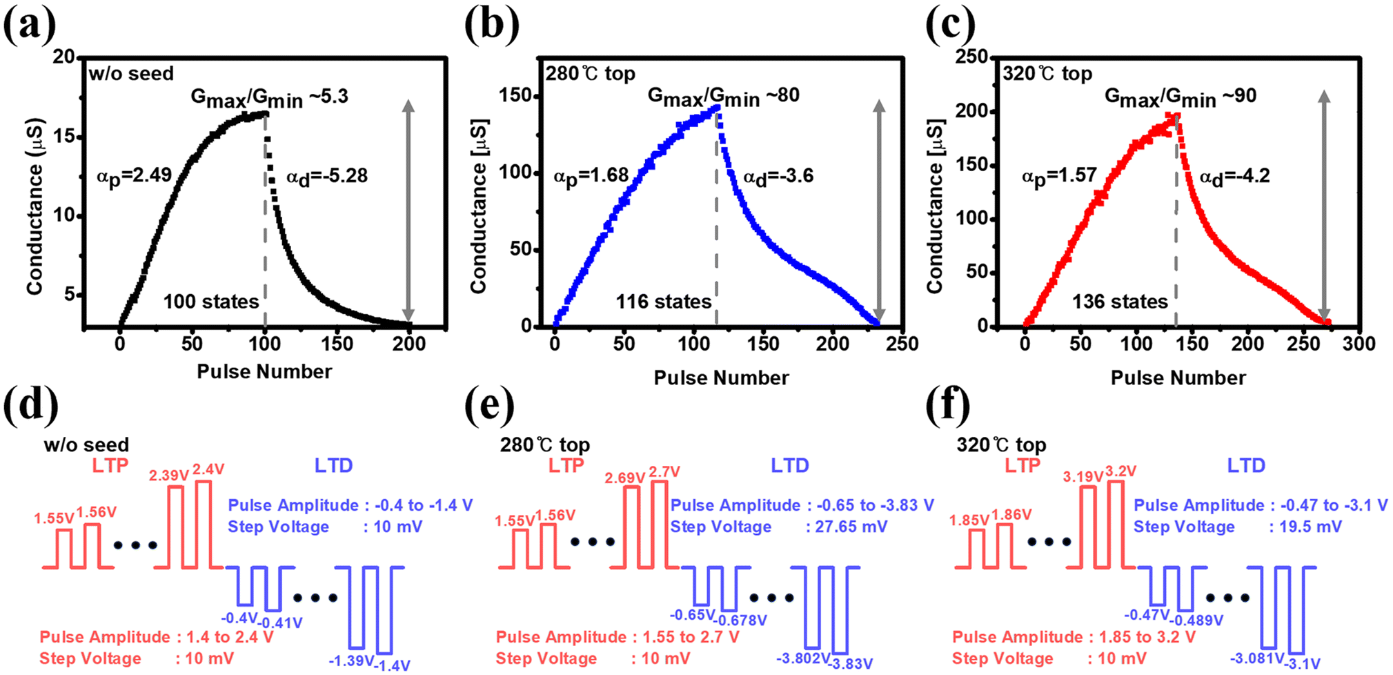 | ||
| Fig. 9 LTP/LTD synaptic characteristics of: (a) FeFET without a seed layer, (b) top layer deposited at 280 °C with SPE and (c) top layer deposited at 320 °C with SPE FeFETs. (d)–(f) Schematic of potentiation/depression incremental pulse waveform. | ||
In order to extract the linearity from the LTP/LTD curves, we analyzed the conductance change as a function of the applied pulse voltage using the following equations:
| Gp = B(1 − e−P/Ap) + Gmin |
| Gd = B(1 − eP−Pmax/Ad) + Gmax |

Here, P, Pmax, Gp, Gd, Ap, Ad and B represent the pulse number, maximum number of pulses, conductance during potentiation, conductance during depression, potentiation linearity, depression linearity, and a fitting factor, respectively. The Ap and Ad values for the device without a seed layer were (2.49, −5.28), indicating poor linearity. However, the devices with top layers deposited at 280 °C and 320 °C showed significant improvements in linearity, with values of (1.68, −3.6) and (1.57, −4.2), respectively. A decrease in grain size increases the number of domains.6 This prevents abrupt polarization switching due to having various polarization directions (various Ec) and shows analog-like incremental behavior rather than digital behavior in potentiation/depression, achieving better linearity.13,45–48 The reason linearity is poorer in depression is due to the behavior of holes. The barrier when a negative gate voltage is applied is thicker than the barrier when a positive gate voltage is applied, making hole tunneling more difficult than electron tunneling. Moreover, electrons are trapped in donor traps near the conduction band where de-trapping can occur at lower energy levels, while holes are trapped in acceptor traps that require relatively high energy to de-trap. Therefore, it is difficult for holes to de-trap and tunnel.49 Consequently, in voltage ranges where hole tunneling is difficult, there is almost no change in conductance until a specific voltage range where tunneling becomes possible, causing a sudden change in conductance. This results in depression showing poorer linearity compared to potentiation.
Finally, to investigate the system-level inference accuracy of our FeFET synaptic devices, we performed simulations using the NeuroSim system-level macro model based on the Modified National Institute of Standards and Technology (MNIST) dataset.50 The neural network used in the simulation was a 2-layer multi-layer perceptron (MLP) comprising 400 input neurons, 100 hidden neurons, and 10 output neurons as depicted in Fig. 10(a). Fig. 10(b) shows the inference accuracy of each device as a function of training epochs. The device without a seed layer achieved an inference accuracy of only ∼65%, which improved to ∼80% with SPE applied. Moreover, the deposition of the top layer at 320 °C resulted in an additional increase in accuracy to ∼85%. This enhancement in inference accuracy is attributed to improvements in linearity, the number of conductance states, and the Gmax/Gmin ratio.
 | ||
| Fig. 10 (a) Schematic of the 2-layer MLP neural network. (b) The inference accuracy for the MNIST handwritten digit image with and without SPE FeFETs. | ||
Conclusion
In this study, we fabricated FeFETs by increasing the ALD deposition temperature and applying the SPE method, and we investigated the impact of these engineering techniques on the memory and synaptic properties. We demonstrated that a significant enhancement in ferroelectric properties was achieved as a result of a reduction in grain size and the higher ALD deposition temperature. Moreover, the device-to-device variation was also improved. The application of these engineering techniques to FeFETs resulted in excellent memory characteristics, including improved MW, Ion/Ioff ratio, and endurance. Furthermore, the synaptic properties, such as the number of conductance states, linearity, and Gmax/Gmin, were significantly improved, ultimately leading to an increase in inference accuracy to 85%. The proposed approach offers a means of controlling the grain size and quality of the ferroelectric film, which in turn allows the manipulation of ferroelectric and synaptic properties.Data availability
Our data in this paper are original and can be accessed under authors’ permission.Conflicts of interest
The authors declare that they have no known competing financial interests or personal relationships that could have appeared to influence the work reported in this paper.Acknowledgements
This research was supported by the National Research Foundation of Korea (NRF) funded by the Ministry of Science, ICT & Future Planning (NRF-2022R1A2C2012333, RS-2022-00154752, no. RS-2023-00260527, and no. RS-2024-00407767). This work was also supported by the Technology Innovation Program (RS-2024-00509266) funded by the Ministry of Trade, Industry & Energy (MOTIE, Korea).References
- G. W. Burr, et al., Neuromorphic computing using non-volatile memory, Adv. Phys.: X, 2017, 2(1), 89–124 Search PubMed.
- W. Zhang, et al., Neuro-inspired computing chips, Nat. Electron., 2020, 3(7), 371–382 Search PubMed.
- Y.-R. Jeon, D. Kim, B. Ku, C. Chung and C. Choi, Synaptic Characteristics of Atomic Layer-Deposited Ferroelectric Lanthanum-Doped HfO2 (La: HfO2) and TaN-Based Artificial Synapses, ACS Appl. Mater. Interfaces, 2023, 15(49), 57359–57368 CAS.
- S. Yu, Neuro-inspired computing with emerging nonvolatile memorys, Proc. IEEE, 2018, 106(2), 260–285 CAS.
- S. Yu, J. Hur, Y.-C. Luo, W. Shim, G. Choe and P. Wang, Ferroelectric HfO2-based synaptic devices: recent trends and prospects, Semicond. Sci. Technol., 2021, 36(10), 104001 CrossRef CAS.
- K. Ni, W. Chakraborty, J. Smith, B. Grisafe and S. Datta, Fundamental understanding and control of device-to-device variation in deeply scaled ferroelectric FETs, in 2019 Symposium on VLSI Technology, 2019: IEEE, pp. T40–T41.
- S. De, et al., Uniform crystal formation and electrical variability reduction in hafnium-oxide-based ferroelectric memory by thermal engineering, ACS Appl. Electron. Mater., 2021, 3(2), 619–628 CrossRef CAS.
- M. H. Park, et al., Ferroelectricity and antiferroelectricity of doped thin HfO2-based films, Adv. Mater., 2015, 27(11), 1811–1831 CrossRef CAS.
- J. Lee, et al., Ferroelectricity of Hf0.5Zr0.5O2 Thin Film Induced at 350 °C by Thermally Accelerated Nucleation During Atomic Layer Deposition, IEEE Trans. Electron Devices, 2024, 71(4), 2690–2695 CAS.
- H. J. Kim, et al., Grain size engineering for ferroelectric Hf0.5Zr0.5O2 films by an insertion of Al2O3 interlayer, Appl. Phys. Lett., 2014, 105(19), 192903–192907 CrossRef.
- D. Zhang et al., Grain size reduction of ferroelectric HZO enabled by a novel solid phase epitaxy (SPE) approach: Working principle, experimental demonstration, and theoretical understanding, in 2023 IEEE Symposium on VLSI Technology and Circuits (VLSI Technology and Circuits), 2023: IEEE, pp. 1–2.
- S. Yu, et al., Multistate Capability Improvement of BEOL Compatible FeFET by Introducing an Al2O3 Interlayer, IEEE Trans. Electron Devices, 2023, 5632–5637 CAS.
- K. A. Aabrar, et al., BEOL-compatible superlattice FEFET analog synapse with improved linearity and symmetry of weight update, IEEE Trans. Electron Devices, 2022, 69(4), 2094–2100 CAS.
- B. C. Johnson, J. C. McCallum and M. J. Aziz, Solid-phase epitaxy, in Handbook of Crystal Growth, Elsevier, 2015, pp. 317–363 Search PubMed.
- M. H. Park, et al., Surface and grain boundary energy as the key enabler of ferroelectricity in nanoscale hafnia-zirconia: A comparison of model and experiment, Nanoscale, 2017, 9(28), 9973–9986 RSC.
- P. Hao, et al., Effects of thickness scaling on the dielectric properties of Hf0.5Zr0.5O2 ferroelectric thin films, J. Mater. Sci.: Mater. Electron., 2023, 34(13), 1089 CAS.
- D. Lehninger, et al., Back-end-of-line compatible low-temperature furnace anneal for ferroelectric hafnium zirconium oxide formation, Phys. Status Solidi A, 2020, 217(8), 1900840 CAS.
- M. H. Park, H. J. Kim, Y. J. Kim, W. Lee, T. Moon and C. S. Hwang, Evolution of phases and ferroelectric properties of thin Hf0.5Zr0.5O2 films according to the thickness and annealing temperature, Appl. Phys. Lett., 2013, 102, 242905 CrossRef.
- Y. H. Lee, et al., Preparation and characterization of ferroelectric Hf0.5Zr0.5O2 thin films grown by reactive sputtering, Nanotechnology, 2017, 28(30), 305703 CrossRef.
- V. Gaddam, D. Das, T. Jung and S. Jeon, Ferroelectricity enhancement in Hf0.5Zr0.5O2 based tri-layer capacitors at low-temperature (350 °C) annealing process, IEEE Electron Device Lett., 2021, 42(6), 812–815 CAS.
- M. H. Park, et al., Understanding the formation of the metastable ferroelectric phase in hafnia–zirconia solid solution thin films, Nanoscale, 2018, 10(2), 716–725 RSC.
- D. Zhang, et al., Grain Size Reduction of Ferroelectric HZO Enabled by Solid Phase Epitaxy (SPE): Working Principle, Experimental Demonstration, and Theoretical Understanding, IEEE Trans. Electron Devices, 2023, 6665–6672 Search PubMed.
- G. Park, et al., Tailoring of Ferroelectric Coercive Field and Polarization with Ferroelectric and Antiferroelectric HfxZr1-xO2 Bilayer Structure, IEEE Electron Device Lett., 2024, 1997–2000 CAS.
- M. H. Park, D. Kwon, U. Schroeder and T. Mikolajick, Binary ferroelectric oxides for future computing paradigms, MRS Bull., 2021, 1–9 Search PubMed.
- M. Materano, et al., Polarization switching in thin doped HfO2 ferroelectric layers, Appl. Phys. Lett., 2020, 117(26), 262904 Search PubMed.
- W. Nix and B. Clemens, Crystallite coalescence: A mechanism for intrinsic tensile stresses in thin films, J. Mater. Res., 1999, 14(8), 3467–3473 Search PubMed.
- B. Ku, Y.-R. Jeon, M. Choi, C. Chung and C. Choi, Effects of post cooling on the remnant polarization and coercive field characteristics of atomic layer deposited Al-doped HfO2 thin films, Appl. Surf. Sci., 2022, 601, 154039 Search PubMed.
- H. Chen, H. Luo, X. Yuan and D. Zhang, Constructing a correlation between ferroelectricity and grain sizes in Hf0.5Zr0.5O2 ferroelectric thin films, CrystEngComm, 2022, 24(9), 1731–1737 Search PubMed.
- Y. Xing, et al., Improved ferroelectricity in cryogenic phase transition of Hf0.5Zr0.5O2, IEEE J. Electron Devices Soc., 2022, 10, 996–1002 CAS.
- K. Park, C. Chung, B. Ku, S. Yun, J. Park and C. Choi, Hf0.5Zr0.5O2/HfO2/Hf0.5Zr0.5O2 Laminated Thin Films and CF4 Plasma Passivation for Improved Memory and Synaptic Characteristics of Ferroelectric Field Effect Transistor, Nanoscale, 2025, 5689–5699 RSC.
- K. Ni, et al., Critical role of interlayer in Hf0.5Zr0.5O2 ferroelectric FET nonvolatile memory performance, IEEE Trans. Electron Devices, 2018, 65(6), 2461–2469 CAS.
- C.-Y. Liao, et al., Multibit ferroelectric FET based on nonidentical double HfZrO2 for high-density nonvolatile memory, IEEE Electron Device Lett., 2021, 42(4), 617–620 CAS.
- N. Tasneem, et al., The impacts of ferroelectric and interfacial layer thicknesses on ferroelectric FET design, IEEE Electron Device Lett., 2021, 42(8), 1156–1159 CAS.
- K. Toprasertpong, M. Takenaka and S. Takagi, Memory window in ferroelectric field-effect transistors: Analytical approach, IEEE Trans. Electron Devices, 2022, 69(12), 7113–7119 CAS.
- M. Su, S. Gao, Z. Weng, L. Zhao, C. Lee and Y. Zhao, Improvement of ferroelectricity and reliability in Hf0.5Zr0.5O2 thin films with two-step oxygen vacancy engineering, IEEE Electron Device Lett., 2022, 43(7), 1057–1060 CAS.
- E. Yurchuk, et al., Charge-trapping phenomena in HfO2-based FeFET-type nonvolatile memories, IEEE Trans. Electron Devices, 2016, 63(9), 3501–3507 CAS.
- Y. Zhang, et al., Interface-Roughness Effect on Polarization Switching and Reliability Performance of Doped-HfO2 Capacitors, IEEE Trans. Electron Devices, 2023, 70(7), 3788–3793 CAS.
- K. Wang, et al., Atomic Layer Deposited ZnO Negative Capacitance Thin-Film Transistors with Hf0.5Zr0.5O2-Based Ferroelectric Gates, IEEE Electron Device Lett., 2024, 2399–2402 CAS.
- X. Li, et al., Re-Annealing-Induced Recovery in 7 nm Hf0.5Zr0.5O2 Ferroelectric Film: Phase Transition and Non-Switchable Region Repair, IEEE Electron Device Lett., 2023, 44(8), 1288–1291 CAS.
- Z. Cai, X. Wang, W. Hong, B. Luo, Q. Zhao and L. Li, Grain–size–dependent dielectric properties in nanograin ferroelectrics, J. Am. Ceram. Soc., 2018, 101(12), 5487–5496 CrossRef CAS.
- D. Das, B. Buyantogtokh, V. Gaddam and S. Jeon, Sub 5 Å-EOT HfxZr1−xO2 for Next-Generation DRAM Capacitors Using Morphotropic Phase Boundary and High-Pressure (200 atm) Annealing With Rapid Cooling Process, IEEE Trans. Electron Devices, 2021, 69(1), 103–108 Search PubMed.
- J. Wang, et al., Excellent ferroelectric properties of Hf0.5Zr0.5O2 thin films induced by Al2O3 dielectric layer, IEEE Electron Device Lett., 2019, 40(12), 1937–1940 CAS.
- Y. Zhang, et al., Enhanced Ferroelectric Properties and Insulator–Metal Transition-Induced Shift of Polarization-Voltage Hysteresis Loop in VOx-Capped Hf0.5Zr0.5O2 Thin Films, ACS Appl. Mater. Interfaces, 2020, 12(36), 40510–40517 CrossRef CAS PubMed.
- P. Li, et al., An unusual mechanism for negative differential resistance in ferroelectric nanocapacitors: polarization switching-induced charge injection followed by charge trapping, ACS Appl. Mater. Interfaces, 2017, 9(32), 27120–27126 CrossRef CAS PubMed.
- S. Yu, et al., Multistate capability improvement of BEOL compatible FeFET by introducing an Al2O3 interlayer, IEEE Trans. Electron Devices, 2023, 70(11), 5632–5637 CAS.
- C.-Y. Liao, et al., Identical pulse programming based ultra-thin 5 nm HfZrO2 ferroelectric field effect transistors with high conductance ratio and linearity potentiation learning trajectory, ECS J. Solid State Sci. Technol., 2021, 10(6), 065015 CrossRef CAS.
- Z.-F. Lou, et al., Identical Pulse With Opposite Polarity Assistance Detrapping—Arithmetic Progression (OPAD-AP) to Ideal Potentiation of FeFET for Synapse, IEEE Trans. Electron Devices, 2024, 7437–7441 CAS.
- K.-Y. Hsiang, et al., Ferroelectric HfZrO2 with electrode engineering and stimulation schemes as symmetric analog synaptic weight element for deep neural network training, IEEE Trans. Electron Devices, 2020, 67(10), 4201–4207 CAS.
- Y. Song, et al., Fatigue of Ferroelectric Field Effect Transistor: Mechanisms and Optimization Strategies, J. Semicond., 2025, 46, 1–14 Search PubMed.
- Y. Luo, X. Peng and S. Yu, MLP + NeuroSimV3.0: Improving On-chip Learning Performance with Device to Algorithm Optimizations, presented at the Proceedings of the International Conference on Neuromorphic Systems, Knoxville, TN, USA, 2019. [Online]. Available: DOI: 10.1145/3354265.3354266.
Footnote |
| † Electronic supplementary information (ESI) available. See DOI: https://doi.org/10.1039/d4nr05381h |
| This journal is © The Royal Society of Chemistry 2025 |