
 Open Access Article
 This Open Access Article is licensed under a Creative Commons Attribution-Non Commercial 3.0 Unported Licence
Synthesis and electronic structure of atomically thin 2H-MoTe2†
Wenjuan
Zhao‡
 *abc,
Xieyu
Zhou‡
d,
Dayu
Yan‡
ab,
Yuan
Huang
*ae,
Cong
Li
ab,
Qiang
Gao
ab,
Paolo
Moras
c,
Polina M.
Sheverdyaeva
c,
Hongtao
Rong
ab,
Yongqing
Cai
ab,
Eike F.
Schwier
f,
Xixia
Zhang
g,
Cheng
Shen
ab,
Yang
Wang
ab,
Yu
Xu
ab,
Wei
Ji
d,
Chen
Liu
h,
Youguo
Shi
a,
Lin
Zhao
a,
Lihong
Bao
a,
Qingyan
Wang
a,
Kenya
Shimada
f,
Xutang
Tao
g,
Guangyu
Zhang
ab,
Hongjun
Gao
ab,
Zuyan
Xu
i,
Xingjiang
Zhou
*abjk and
Guodong
Liu
*abj
*abc,
Xieyu
Zhou‡
d,
Dayu
Yan‡
ab,
Yuan
Huang
*ae,
Cong
Li
ab,
Qiang
Gao
ab,
Paolo
Moras
c,
Polina M.
Sheverdyaeva
c,
Hongtao
Rong
ab,
Yongqing
Cai
ab,
Eike F.
Schwier
f,
Xixia
Zhang
g,
Cheng
Shen
ab,
Yang
Wang
ab,
Yu
Xu
ab,
Wei
Ji
d,
Chen
Liu
h,
Youguo
Shi
a,
Lin
Zhao
a,
Lihong
Bao
a,
Qingyan
Wang
a,
Kenya
Shimada
f,
Xutang
Tao
g,
Guangyu
Zhang
ab,
Hongjun
Gao
ab,
Zuyan
Xu
i,
Xingjiang
Zhou
*abjk and
Guodong
Liu
*abj
aBeijing National Laboratory for Condensed Matter Physics, Institute of Physics, Chinese Academy of Sciences, Beijing 100190, China. E-mail: Wenjuan.Zhao@trieste.ism.cnr.it; yhuang01@iphy.ac.cn; XJZhou@iphy.ac.cn; gdliu_arpes@iphy.ac.cn
bUniversity of Chinese Academy of Sciences, Beijing 100049, China
cCNR-Istituto di Struttura della Materia (CNR-ISM), SS 14, Km 163, 5, 34149 Trieste, Italy
dDepartment of Physics, Renmin University of China, Beijing 100872, P.R. China
eSchool of Physics, School of Integrated Circuits and Electronics, Beijing Institute of Technology, Advanced Research Institute of Multidisciplinary Sciences, Beijing 100081, China
fResearch Institute for Synchrotron Radiation Science (HiSOR), Hiroshima University, Higashi-Hiroshima, Hiroshima 739-0046, Japan
gState Key Laboratory of Crystal Materials, Shandong University, 250100, Jinan, Shandong, China
hInstitute of High Energy Physics, Chinese Academy of Sciences, Beijing 100049, China
iTechnical Institute of Physics and Chemistry, Chinese Academy of Sciences, Beijing 100190, China
jSongshan Lake Materials Laboratory, Dongguan 523808, China
kBeijing Academy of Quantum Information Sciences, Beijing 100193, China
First published on 26th March 2025
Abstract
An in-depth understanding of the electronic structure of 2H-MoTe2 at the atomic layer limit is a crucial step towards its exploitation in nanoscale devices. Here, we show that millimeter-sized monolayer (ML) MoTe2 samples, as well as smaller sized bilayer (BL) samples, can be obtained using the mechanical exfoliation technique. The electronic structure of these materials is investigated by angle-resolved photoemission spectroscopy (ARPES) for the first time and by density functional theory (DFT) calculations. The comparison between experiments and theory allows us to describe ML MoTe2 as a semiconductor with a direct gap at the K point. This scenario is reinforced by the experimental observation of the conduction band minimum at K in Rb-doped ML MoTe2, resulting in a gap of at least 0.924 eV. In the BL MoTe2 system, the maxima of the bands at Γ and K show very similar energies, thus leaving the door open to a direct gap scenario, in analogy to WSe2. The monotonic increase in the separation between spin-split bands at K while moving from ML to BL and bulk-like MoTe2 is attributed to interlayer coupling. Our findings can be considered as a reference to understand quantum anomalous and fractional quantum anomalous Hall effects recently discovered in ML and BL MoTe2 based moiré heterostructures.
1 Introduction
Monolayer transition metal dichalcogenides (TMDCs) with the formula MX2 (where M = Mo and W; X = S, Se, and Te) and 2H phase exhibit unique and remarkable properties, including direct band gap transition,1–4 well-defined valley degrees of freedom and spin-valley locking,5 huge exciton binding energy,6,7 and Ising superconductivity.8 Their unique properties can lead to numerous applications in next-generation nanoelectronics,9 optoelectronics,10 and valleytronics.7MoTe2 is a small gap semiconductor hosting exotic and prominent quantum phenomena in the few layer limit.11–13 Recently, the quantum anomalous Hall effect (QAH, also referred to as the integer Chern insulating state) has been reported in twisted bilayer (BL) MoTe2![[thin space (1/6-em)]](https://www.rsc.org/images/entities/char_2009.gif) 13 and in AB-stacked MoTe2/WSe2 moiré hetero-BLs.12 The long-sought-after fractional quantum anomalous Hall effect (FQAH, also called the fractional Chern insulating state) has been discovered only in twisted BL MoTe2,13–16 although it had been predicted in some twisted TMDC moiré BLs.12,17–19 Thus, the rhombohedrally stacked twisted MoTe2-based BLs have emerged as a promising platform for investigating both QAH and FQAH effects at zero magnetic field. Additionally, a giant intrinsic spin Hall effect has also been found in AB-stacked MoTe2/WSe2 moiré BLs.20–22 These findings pay the way for investigating novel physical properties such as fractional charge excitation and anyon statistics under zero magnetic field conditions, thus providing new opportunities for dissipationless transport, topological quantum computing and spintronics.13–16,20,23 In spite of the importance of MoTe2, there have been no reports on the electronic band structures of monolayer (ML) MoTe2, which is the ultimate building block of the moiré heterostructures mentioned above.
13 and in AB-stacked MoTe2/WSe2 moiré hetero-BLs.12 The long-sought-after fractional quantum anomalous Hall effect (FQAH, also called the fractional Chern insulating state) has been discovered only in twisted BL MoTe2,13–16 although it had been predicted in some twisted TMDC moiré BLs.12,17–19 Thus, the rhombohedrally stacked twisted MoTe2-based BLs have emerged as a promising platform for investigating both QAH and FQAH effects at zero magnetic field. Additionally, a giant intrinsic spin Hall effect has also been found in AB-stacked MoTe2/WSe2 moiré BLs.20–22 These findings pay the way for investigating novel physical properties such as fractional charge excitation and anyon statistics under zero magnetic field conditions, thus providing new opportunities for dissipationless transport, topological quantum computing and spintronics.13–16,20,23 In spite of the importance of MoTe2, there have been no reports on the electronic band structures of monolayer (ML) MoTe2, which is the ultimate building block of the moiré heterostructures mentioned above.
Compared to the molecular beam epitaxy growth method,24 mechanical exfoliation is a simpler and more universal technique. It typically results in weaker substrate interactions and yields higher quality samples.25 In this paper, we report on the synthesis of millimeter-sized ML MoTe2 samples via the mechanical exfoliation method. The superior structural uniformity of the so-obtained layers allows us to perform detailed characterization of their properties by space-averaging techniques, such as low-energy electron diffraction (LEED), Raman spectroscopy and, for the first time, angle-resolved photoemission spectroscopy (ARPES). The electronic structure of ML MoTe2 displays a flat state around Γ and a valence band maximum (VBM) at the K point, which are well reproduced by density functional theory (DFT) calculations. On the basis of this agreement, the system can be described as a semiconductor with a direct gap at the K point. The observation of conduction band filling at K in Rb-doped ML MoTe2 strengthens this scenario. Occasionally, mechanical exfoliation gives rise to well-ordered patches of BL MoTe2 surrounded by areas of ML and multilayer (bulk-like) MoTe2. The topmost occupied states at Γ and K in these BLs exhibit similar binding energy. This may suggest that BL MoTe2 is a direct gap semiconductor, in analogy to BL WSe2.26 Finally, we discover that the energy separation of the spin-split states at K increases monotonically from ML to BL and to multilayer MoTe2 as a consequence of interlayer coupling. Our work sheds light on the electronic structure of atomically thin MoTe2 layers, thus providing fundamental support to understand the origin of QAH and FQAH effects occurring in MoTe2-based heterostructures.
2. Methods
ML, BL and multilayer (bulk-like) MoTe2 flakes were prepared by the mechanical exfoliation method from bulk crystals, as illustrated in Fig. 1(a).25 ARPES measurements on ML and multilayer (more than 10 MLs) samples were performed with a photon energy of 21.218 eV, using a home-built photoemission spectroscopy system27 equipped with a VUV5000 helium lamp (spot size: 0.8 mm × 0.8 mm) and a DA30L electron energy analyzer (Scienta Omicron). The overall energy resolution was set to 20 meV, and the angular resolution to 0.2°. ARPES data of BL samples were collected at the BL-1 end station of HiSOR with a photon energy of 45 eV (spot size: 0.8 mm × 0.3 mm). All the samples were measured at 30–40 K under a base pressure better than 5 × 10⁻¹¹ mbar, after mild vacuum annealing at about 500 K.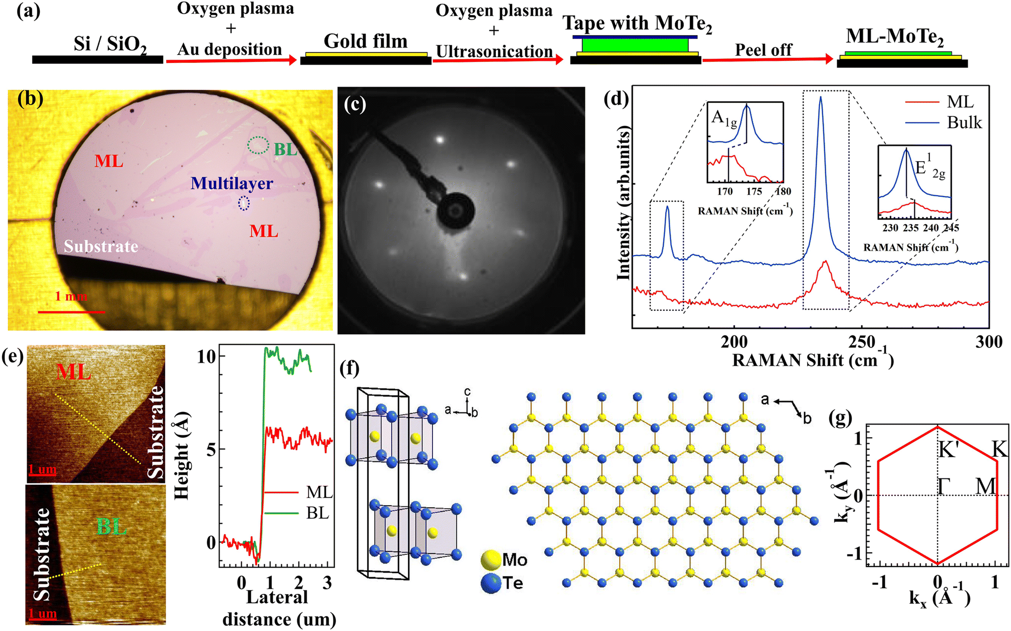 | ||
| Fig. 1 (a) Cartoon illustrating the sample fabrication process. Black, yellow, green, and blue rectangular bars represent the SiO2/Si wafer, gold film, MoTe2 layer, and adhesive tape, respectively. (b) Typical optical microscopy image of a sample after mechanical exfoliation of MoTe2. The predominant pink areas are millimeter-sized domains of ML MoTe2 in contact with the substrate (dark pink areas). Small light pink and white areas surrounded by dotted ovals represent BL and multilayer MoTe2, respectively. (c) LEED pattern taken on a sample with prevalent ML MoTe2 coverage. (d) Raman spectra of ML (red) and bulk (blue) MoTe2. Characteristic peaks are highlighted in the insets. (e) AFM images taken at the edge between the Au substrate and ML (top panel) and BL (bottom panel) MoTe2 domains. The thickness profiles extracted from the lines shown in the AFM images are compared in the right panel. (f) Crystal structure of MoTe2 in isometric and top views. (g) SBZ of MoTe2. | ||
DFT calculations were performed using the generalized gradient approximation and the projector augmented wave method28,29 as implemented in the Vienna ab initio simulation package (VASP).30,31 A uniform Monkhorst–Pack k mesh of 21 × 21 × 5 was adopted for integration over the Brillouin zone of bulk MoTe2, and a mesh of 21 × 21 × 1 was used for ML and BL MoTe2. A plane-wave cutoff energy of 700 eV was used for structural relaxation and electronic structure calculations. A distance of more than 15 Å along the out-of-plane direction was adopted to eliminate interaction between adjacent layers. Dispersion correction was made using the van der Waals Density Functional (vdW-DF) approach,32–34 with the optB86b functional for the exchange potential, which was proved to be accurate in describing the structural properties of layered materials35–40 and was adopted for structure related calculations. All atoms were allowed to relax until the residual force per atom was less than 0.01 eV Å−1. In our electronic structure calculations, we used the Perdew–Burke–Ernzerhof (PBE)41 functional with consideration of spin–orbit coupling (SOC), based on the vdW-DF optimized atomic structures. A plane-wave cutoff energy of 500 eV and a k mesh of 9 × 9 × 3 were used for energy calculations for bulk MoTe2 (9 × 9 × 1 for ML and BL).
3 Results and discussion
Fig. 1(a) illustrates the sample preparation procedure of atomically thin MoTe2 samples by the mechanical exfoliation method.25 The SiO2/Si substrate (black rectangle) is cleaned using oxygen plasma, covered with a 3–20 nm thick layer of gold (yellow rectangle) and cleaned again using oxygen plasma and ultrasonication. Adhesive tape (blue rectangle) loaded with a bulk MoTe2 layer (green rectangle) is brought into contact with the substrate and then removed to complete the exfoliation process. Fig. 1(b–e) show the characterization of samples prepared according to this procedure. Typically, optical microscopy images (Fig. 1(b)) reveal the presence of millimeter-sized MoTe2 domains (pink areas) covering most of the substrate (dark pink areas). After mild annealing (500 K) under ultra-high vacuum conditions, a sharp hexagonal LEED pattern becomes visible (Fig. 1(c)), thus indicating the long-range order of the MoTe2 domains. In order to determine the vibrational properties of these domains, Fig. 1(d) compares the Raman data acquired on the pink area shown in Fig. 1(b) (red spectrum) and on bulk-like (more than 10 MLs) MoTe2 (blue spectrum) with a laser wavelength of 532 nm. In the blue spectrum, the A1g mode is located at 173.67 cm−1 and the E2g1 mode at 233.87 cm−1, while in the red spectrum they are found at 170.58 cm−1 and 235.92 cm−1, respectively (insets in Fig. 1(d)). These shifts from the reference bulk-like values are consistent with previously reported results for ML MoTe2.42 The topmost atomic force microscopy (AFM) image in Fig. 1(e) directly shows that the height difference between the substrate and the millimeter-sized MoTe2 domains is 5.97 ± 1 Å (red line in the right panel), which is in the range of the expected thickness of ML MoTe2 (6.98 Å). Overall, these experimental data allow us to identify the pink areas of Fig. 1(b) as well-ordered domains of ML MoTe2.Fig. 1(b) also displays small regions (typical size in the order of 0.1 mm) with light pink and white optical contrast. The AFM analysis of the light pink areas (bottommost image in Fig. 1(e)) shows that their height with respect to the substrate corresponds to 10.32 ± 1 Å, i.e. nearly twice the measured thickness of ML MoTe2. Therefore, these areas are identified as domains of BL MoTe2. Finally, the white areas are bulk-like multilayers of MoTe2. Occasionally, the mechanical exfoliation method produces millimeter sized areas of BL and multilayer (from here onwards called bulk) MoTe2, which allow space-averaging ARPES analysis, as shown in Fig. 2. Fig. S1 in the ESI†43 shows the structural characterization of a sample with BL domains on the order of 1 mm2, where the thickness of the BL areas is measured by AFM and confirmed by cross-sectional transmission electron microscopy.
 | ||
| Fig. 2 (a–c) ARPES maps illustrating the electronic band structures along the M–Γ–K–M high symmetry direction in ML (a), BL (b), and bulk (c) MoTe2, as indicated at the top. The inset in (a) shows the high symmetry directions (red dashed lines) in the SBZ (green hexagon). The lower panels (d–f) depict the second derivative plots of panels (a–c), respectively. The red dotted curves overlaid on the plots represent the corresponding bands calculated by DFT. | ||
For reference, Fig. 1(f) displays the crystal structure of 2H-MoTe2, which comprises van der Waals Te–Mo–Te trilayers (left panel) stacked along the c-axis and forming a honeycomb lattice in the (0001) projection plane (right panel). The prisms of adjacent trilayers point in opposite directions within the plane. Among the TMDCs, MoTe2 possesses notably large lattice parameters (a = 3.52 Å and c = 13.97 Å).44Fig. 1(g) presents the surface Brillouin zone (SBZ) of MoTe2, along with high symmetry points, which will be useful for the discussion of the ARPES data.
Fig. 2 reports an overview of the ARPES analysis along the M–Γ–K–M path for ML (Fig. 2(a and d)) and BL (Fig. 2(b and e)) taken on a millimeter sized domain of the sample shown in Fig. S1† and bulk (Fig. 2(c and f)) MoTe2. The spectra are shown as acquired in the top row and after second derivative treatment (along the energy axis) in the bottom row, to enhance the sensitivity to weak electronic features. The well-defined Fermi level (EF) observed in the second derivative data derives from the partially uncovered Au layer in the substrate. The calculated band structures (red dotted lines) are overlaid on the data in the bottom row of the figure (see Fig. S2 in the ESI† for calculations extended above EF43).
In the ML sample (Fig. 2(a and d)), the topmost band observed near Γ is very flat and mainly derives from Mo dz2 orbitals, with a minor Te pz contribution, which exhibits significant localization in the lattice plane (calculations of the orbital character are reported in Fig. S3 in the ESI†43). The two parabolic-like bands with maxima at the K point primarily derive from in-plane delocalized Mo dx2−y2/dxy orbitals, with a small contribution from Te px/py orbitals. These bands form a spin–split pair, originating from the strong SOC of Mo atoms and the absence of structural inversion symmetry, and become degenerate along the Γ–M direction due to time-reversal symmetry. The VBM is found at K (−0.76 eV), which lies well above the topmost state at Γ (−1.375 eV) (see also Fig. S4 in the ESI†). The observations of a flat band at Γ and the VBM at K are consistent with those of other ML-MX2 materials.26,45–47 In addition to these characteristic features, two parabolic bands centered at the M point with energies ∼−1.25 eV and −1.7 eV, as well as another parabolic band centered at the Γ point around −2 eV, are discernible. The increasing background below −2 eV in Fig. 2(a and d) originates from the intense 5d states of the underlying polycrystalline gold substrate. The experimental band structure of the ML MoTe2 sample within the first 2 eV below EF turns out to be well reproduced by the calculations (Fig. 2(d)). This good correspondence allows us to describe ML MoTe2 as a direct band gap semiconductor.
Fig. 3 presents further data supporting the direct band gap scenario in ML MoTe2. To directly determine the momentum position of the conduction band minimum (CBM), Rb atoms are evaporated on the surface of ML MoTe2 to partially fill its unoccupied bands.48 The changes induced by Rb deposition in the band structure of ML MoTe2 along the Γ–K direction are shown in Fig. 3(a–d). As the amount of deposited Rb increases, the bands shift continuously away from EF (Fig. 3(b–d)). At the highest Rb coverage (Fig. 3(d)), the VBM and the topmost state at Γ are located at −0.96 and −1.66 eV. The detailed evolution of the bands at the Γ and K points is depicted through the energy distribution curves (EDCs) taken at the k|| positions marked by the orange dashed lines in Fig. 3(a) and illustrated in Fig. 3(e) and (f), respectively. These EDCs demonstrate a peak shift of 0.285 eV at the Γ point and 0.2 eV at the K point. These data indicate a non-rigid band shift that could be used for electronic structure engineering of ML MoTe2.
 | ||
| Fig. 3 Direct band gap observation in ML MoTe2 through Rb deposition. ARPES data of (a) pristine and (b–d) Rb-doped MoTe2 ML measured along cut 1 (Γ–K direction) as shown in the inset of panel (a). (e and f) EDCs at the Γ and K points extracted from panels (a–d), respectively. The red and green dashed lines mark the positions of the band maxima for the pristine MoTe2 sample and after the 3rd Rb deposition. (g) ARPES data along cut 2 after the 3rd Rb deposition, where a new band appears near EF at K′ (see the inset). (h) EDCs at K′ for pristine MoTe2 (red) and after the 3rd Rb deposition (green). | ||
Interestingly, the spectra acquired in the proximity of K′ (cut 2 in the inset of Fig. 3(a)) for the highest Rb deposition display a peak near EF (inset in Fig. 3(g)). The emergence of this feature can be observed in Fig. 3(h), which shows the EDCs extracted at K′ for both pristine (red) and highly Rb doped MoTe2 (green). The peak is identified as the CBM at the K′ point. Together with the VBM at the K/K′ point, this new state proves the existence of a direct gap of at least 0.924 eV. This gap value is different from that of pristine MoTe2 because of band renormalization effects, which clearly manifest in the non-rigid Rb-induced band shifts. However, it is close to the gap size expected from the DFT calculation (0.97 eV, Fig. S3†). This observation is in line with other band calculations,43,49,50 photoluminescence49,51,52 and STS24 measurements for ML MoTe2.
BL and bulk MoTe2 exhibit electronic bands similar to those of the ML case with differences mainly concentrated around the Γ point. In Fig. 2(b and e), an additional parabolic band is present above the flat band. In Fig. 2(c and f), a complex packed structure of parabolic bands is observed above the flat band, which is consistent with the reported results for more than 3 ML thick MoTe2 samples.11,48 The orbital calculation in Fig. S3†43 indicates that the parabolic band (BL) and the packet of bands (bulk) can be explained by the repulsion between Mo dz2 and Te pz orbitals perpendicular to the plane. This repulsion increases the energy at Γ in BL and bulk MoTe2 and reduces the energy from Γ to M and Γ to K because of the increasing component of in-plane orbitals. Below the flat band, the parabolic bands become clearer in BL and bulk MoTe2 samples.
It is worth noting that the topmost valence states of BL MoTe2 at both Γ and K are located at −0.795 eV (a detailed comparison is provided in Fig. S5 in the ESI†43). This situation is analogous to that observed in BL WSe2, which is predicted to be a direct gap semiconductor,26,53,54 but contrasts with most indirect-gap BL TMDC semiconductors, such as MoS2, WS2, and MoSe2, where the VBM is found at Γ.45,53,55–57 Our ARPES data may suggest the presence of a direct gap at K in BL MoTe2, which would be consistent with the results of low-temperature photoluminescence experiments.51,58,59 However, our calculations (Fig. S2†43) reveal that the CBM is located halfway between Γ and K. This inconsistency can be attributed to the slight lattice mismatch between the calculated freestanding BL and the real BL MoTe2 on the Au substrate, which was not considered in our calculations.60,61 ARPES is inherently unable to directly observe the conduction band due to the lack of electron occupation, thus precluding the verification of the CBM position through this method. Further investigation is required to clarify the nature (direct vs. indirect gap semiconductor) of BL MoTe2.
For bulk MoTe2, the topmost valence state at the Γ point (−0.665 eV) is closer to EF than that at K (−0.87 eV), thus indicating a typical indirect gap semiconductor behavior. Overall, the valence band structures in Fig. 2 provide clear evidence for the indirect-to-direct band gap transition with decreasing layer thickness from bulk (indirect gap) to ML (direct gap). This transition originates from the quantum confinement effect2,62 and is consistent with reported photoluminescence results.49,51,52,63
The splitting of the valence bands (VB1 and VB2) near the K point holds significance for various crucial phenomena and properties of MX2 materials, including spin-valley locking, the AB exciton effect,6,7 and spin-layer locking.64 In Fig. 4, we show ARPES data along the Γ–K direction for ML, BL and bulk samples (Fig. 4(a–c)) and the corresponding second derivative plots (Fig. 4(d–f)). To facilitate a quantitative comparison, Fig. 4(g–i) display EDCs at the K point for the different samples. The measured splitting at K increases monotonically with thickness (details of the Gaussian fitting are given in Fig. S6†43): 0.212 eV in ML, 0.225 eV in BL and 0.252 eV in bulk MoTe2. These data are consistent with the trend of the DFT results, which give 0.22, 0.24, and 0.31 eV for the respective systems. Generally, in the family of MX2 TMDCs, the valence band splitting around the K point arises from SOC, inversion symmetry breaking, and interlayer coupling.5 The increasing splitting size can be attributed to a variation of the interlayer coupling strengths between BL or bulk (Fig. S7†43) and ML MoTe2.5,65 Therefore, our observations imply an interlayer interaction strength in the order of 10 meV and 40 meV for BL and bulk MoTe2, respectively. The increased interlayer coupling strength from BL to bulk is likely to be a consequence of the reduced layer separation as the number of layers increases, thereby enhancing interlayer hopping and coupling.65
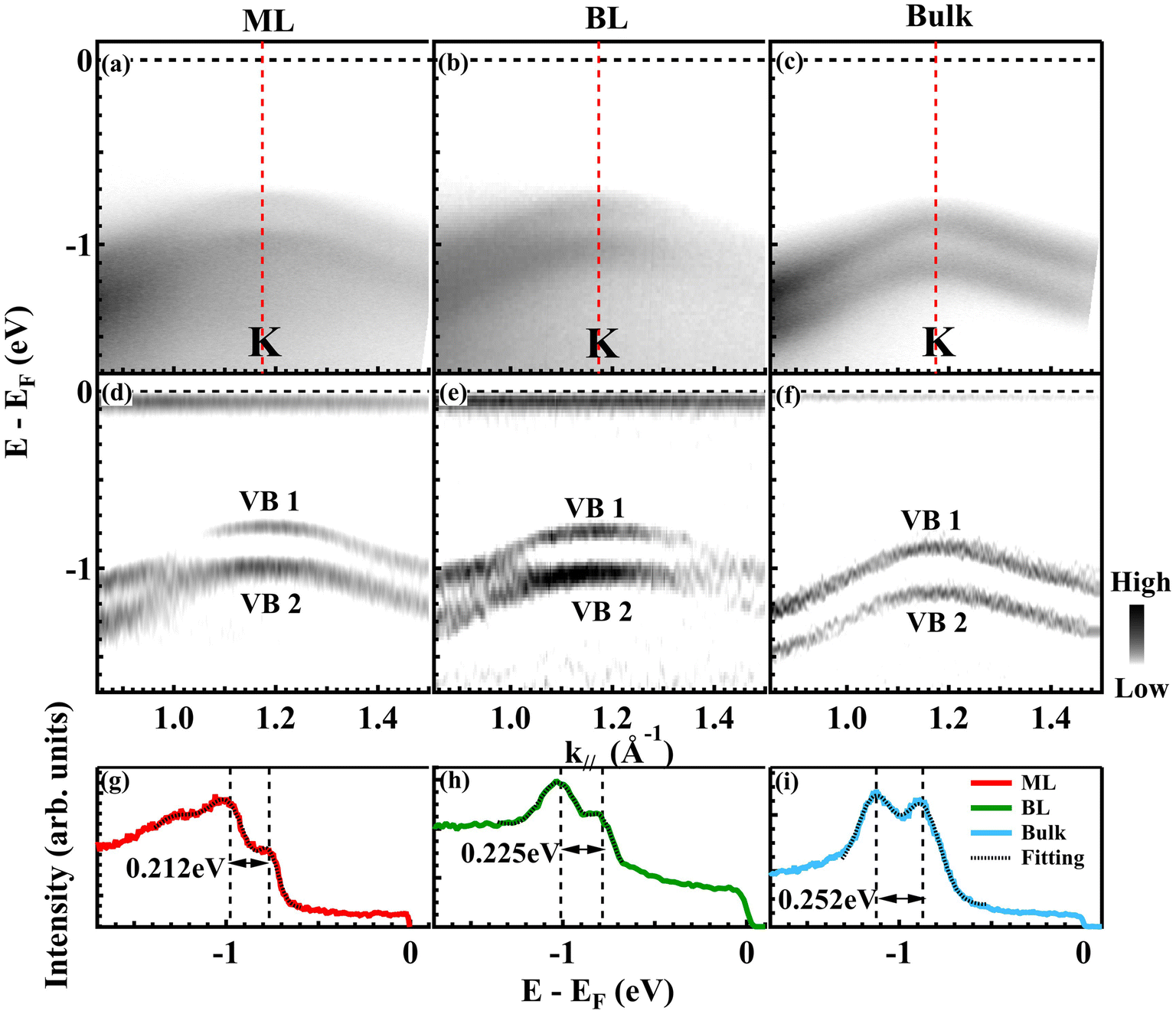 | ||
| Fig. 4 Layer dependent band splitting at K. (a–c) ARPES maps showing the valence band splitting around K along the Γ–K–M direction for ML, BL and bulk MoTe2, respectively. (d–f) Second derivative spectra of (a–c) along the energy axis, respectively. (g–i) EDCs at K from (a–c), shown as red (ML), green (BL) and blue (bulk) curves, respectively. The black dotted curves are the corresponding Gaussian fitting results, with peak positions indicated by black dashed lines. | ||
The splitting of spin-polarized bands is a distinctive feature of ML-TMDCs, resulting from the interplay of SOC and the breaking of inversion symmetry.5,66,67 The splitting in ML MoSe2 is ∼0.18 eV (ref. 45) and in ML MoS2 is ∼0.15 eV.46 The larger splitting that we observed in ML MoTe2 is a consequence of the larger SOC of Te with respect to Se and S. This characteristic makes ML MoTe2 particularly well-suited for applications in spintronics.
To summarize our results in a quantitative way, we have compiled Table 1 with the relevant parameters of the band structures for the different MoTe2 systems derived from ARPES measurements and DFT calculations. Regarding the K splitting, the difference between the VBM at the K and Γ points, and the size of the direct band gap in ML MoTe2, our calculations show consistent results with the ARPES measurements as discussed above. We have also derived the effective mass near the VBM at both K and Γ points along the Γ–K direction (details in Table S1†43). While going from ML to BL and bulk, the observed effective mass at K shows similar values for the different layered samples. Conversely, at Γ, both the observed and calculated hole effective masses for the top of the valence band exhibit a rapid and monotonic decrease as the number of layers increases. The discrepancy between the experimental (13.09m0) and calculated (34.52m0) effective masses at the Γ point for ML MoTe2 primarily arises from hybridization between the MoTe2 and Au states. Our DFT calculations were performed for free-standing MoTe2 layers. Therefore, the interaction with the substrate is not taken into account. The effective mass of the Au sp states (<1 electron mass68) is much lower than that of ML MoTe2. As a result of the MoTe2–Au interaction, the measured effective mass is lower than the calculated one. A similar effect has been reported in the case of ML MoS2.69 Importantly, all ARPES analyses and DFT calculations are consistent.
| Thickness | ML | BL | Bulk | |||
|---|---|---|---|---|---|---|
| ARPES | Calculation | ARPES | Calculation | ARPES | Calculation | |
| a The value extracted from the ML sample after Rb deposition. m0 is the electron mass | ||||||
| Splitting at K [eV] | 0.212 | 0.22 | 0.225 | 0.24 | 0.252 | 0.31 |
| Energy difference between VBM at K and Γ [eV] | 0.615 | 0.536 | 0 | 0.059 | −0.205 | −0.005 |
| Gap size [eV] | 0.924a | 0.97 | — | 0.91 | — | 0.72 |
| Effective mass at K [m0] | 1.17 | 0.59 | 1.69 | 0.62 | 1.56 | 0.61 |
| Effective mass at Γ [m0] | 13.09 | 34.52 | 5 | 8.5 | — | 1.27 |
4. Conclusions
In summary, we report on the synthesis of millimeter-sized ML MoTe2 domains using the mechanical exfoliation method. The exceptional structural uniformity of these layers allows for comprehensive characterization using space-averaging techniques. Our investigation reveals that the electronic structure of ML MoTe2 features a flat band around the Γ point and a VBM at the K point, in agreement with DFT calculations. This strongly suggests that the material can be described as a semiconductor with a direct band gap at K. The observation of conduction band filling at K in Rb-doped ML MoTe2, with a direct band gap of at least 0.924 eV, further supports this interpretation. The topmost occupied states of BL MoTe2 at Γ and K exhibit similar binding energies. This opens the possibility that BL MoTe2 is a direct gap system, akin to WSe2. Finally, the energy separation of the spin-split bands at K increases monotonically from ML to BL to bulk MoTe2 due to interlayer coupling. The present work sheds light on the electronic structure of atomically thin MoTe2 layers, which could be significant in clarifying the origin of quantum anomalous Hall (QAH) and fractional quantum anomalous Hall (FQAH) effects observed in MoTe2-based heterostructures.Author contributions
W.Z., Xie. Z. and D.Y. contributed equally to this work. G.L., Xin. Z. and W.Z. conceptualized the work; W.Z., Q.G., H.R., E.F.S., Y.W., L.Z., K.S. and G.L. conducted the ARPES experiments; C. L., Y.C., Y.X., L.B. and Z.X. provided instrumental support for the ARPES measurements; W.Z., G.L., P.M. and P.M.S. wrote the article with contributions from all coauthors; D.Y., Y.H., Xix. Z., C.S., C.L., Y.S., Q.W., X.T., G.Z., and H.G. prepared the samples and performed the Raman, AFM and XPS measurements; Xie. Z. and W.J. conducted the DFT calculations; Y.H., G.L. and Xin. Z. supported the network. W.Z., Y.H., Xin. Z. and G.L. are the corresponding authors.Data availability
The data supporting this article have been included as part of the ESI.†43Conflicts of interest
There are no conflicts to declare.Acknowledgements
This work is supported by the National Key Research and Development Program of China (No. 2022YFA1403901, 2019YFA0308000 and 2018YFA0704201), the National Natural Science Foundation of China (No. 11574367 and 11874405), and the Youth Innovation Promotion Association of Chinese Academy of Sciences (No. 2017013 and 2019007). PM and PMS acknowledge partial funding through the project EUROFEL-ROADMAP ESFRI of the Italian Ministry of University and Research. Synchrotron ARPES measurements were performed under the approval of the Program Advisory Committee of HiSOR (proposal numbers: 17BU004, 17BU005 and 18AU001).References
- J. K. Ellis, M. J. Lucero and G. E. Scuseria, Appl. Phys. Lett., 2011, 99, 261908 CrossRef.
- Z. Y. Zhu, Y. C. Cheng and U. Schwingenschlögl, Phys. Rev. B:Condens. Matter Mater. Phys., 2011, 84, 153402 CrossRef.
- T. Cheiwchanchamnangij and W. R. L. Lambrecht, Phys. Rev. B:Condens. Matter Mater. Phys., 2012, 85, 205302 CrossRef.
- A. Kumar and P. K. Ahluwalia, Eur. Phys. J. B, 2012, 85, 186 CrossRef.
- D. Xiao, G.-B. Liu, W. Feng, X. Xu and W. Yao, Phys. Rev. Lett., 2012, 108, 196802 CrossRef PubMed.
- M. M. Ugeda, A. J. Bradley, S.-F. Shi, F. H. da Jornada, Y. Zhang, D. Y. Qiu, W. Ruan, S.-K. Mo, Z. Hussain, Z.-X. Shen, F. Wang, S. G. Louie and M. F. Crommie, Nat. Mater., 2014, 13, 1091–1095 CrossRef CAS PubMed.
- J. R. Schaibley, H. Yu, G. Clark, P. Rivera, J. S. Ross, K. L. Seyler, W. Yao and X. Xu, Nat. Rev. Mater., 2016, 1, 16055 CrossRef CAS.
- J. M. Lu, O. Zheliuk, I. Leermakers, N. F. Q. Yuan, U. Zeitler, K. T. Law and J. T. Ye, Science, 2015, 350, 1353–1357 CrossRef CAS.
- B. Radisavljevic, A. Radenovic, J. Brivio, V. Giacometti and A. Kis, Nat. Nanotechnol., 2011, 6, 147–150 CrossRef CAS PubMed.
- S. Manzeli, D. Ovchinnikov, D. Pasquier, O. V. Yazyev and A. Kis, Nat. Rev. Mater., 2017, 2, 17033 CrossRef CAS.
- H. Zhang, C. Bao, Z. Jiang, K. Zhang, H. Li, C. Chen, J. Avila, Y. Wu, W. Duan, M. C. Asensio and S. Zhou, Nano Lett., 2018, 18, 4664–4668 CrossRef CAS PubMed.
- H. Li, U. Kumar, K. Sun and S.-Z. Lin, Phys. Rev. Res., 2021, 3, L032070 CrossRef CAS.
- H. Park, J. Cai, E. Anderson, Y. Zhang, J. Zhu, X. Liu, C. Wang, W. Holtzmann, C. Hu, Z. Liu, T. Taniguchi, K. Watanabe, J.-H. Chu, T. Cao, L. Fu, W. Yao, C.-Z. Chang, D. Cobden, D. Xiao and X. Xu, Nature, 2023, 622, 74–79 CrossRef CAS PubMed.
- Y. Zeng, Z. Xia, K. Kang, J. Zhu, P. Knüppel, C. Vaswani, K. Watanabe, T. Taniguchi, K. F. Mak and J. Shan, Nature, 2023, 622, 69–73 CrossRef CAS PubMed.
- J. Cai, E. Anderson, C. Wang, X. Zhang, X. Liu, W. Holtzmann, Y. Zhang, F. Fan, T. Taniguchi, K. Watanabe, Y. Ran, T. Cao, L. Fu, D. Xiao, W. Yao and X. Xu, Nature, 2023, 622, 63–68 CrossRef CAS PubMed.
- F. Xu, Z. Sun, T. Jia, C. Liu, C. Xu, C. Li, Y. Gu, K. Watanabe, T. Taniguchi and B. Tong, et al. , Phys. Rev. X, 2023, 13, 031037 CAS.
- F. Wu, T. Lovorn, E. Tutuc, I. Martin and A. H. MacDonald, Phys. Rev. Lett., 2019, 122, 086402 CrossRef CAS PubMed.
- T. Devakul, V. Crépel, Y. Zhang and L. Fu, Nat. Commun., 2021, 12, 6730 CrossRef CAS PubMed.
- V. Crépel and L. Fu, Phys. Rev. B, 2023, 107, L201109 CrossRef.
- Z. Tao, B. Shen, W. Zhao, N. C. Hu, T. Li, S. Jiang, L. Li, K. Watanabe, T. Taniguchi, A. H. MacDonald, J. Shan and K. F. Mak, Nat. Nanotechnol., 2024, 19, 28–33 CrossRef CAS PubMed.
- W. Zhao, K. Kang, Y. Zhang, P. Knüppel, Z. Tao, L. Li, C. L. Tschirhart, E. Redekop, K. Watanabe, T. Taniguchi, A. F. Young, J. Shan and K. F. Mak, Nat. Phys., 2024, 20, 275–280 Search PubMed.
- T. Li, S. Jiang, B. Shen, Y. Zhang, L. Li, Z. Tao, T. Devakul, K. Watanabe, T. Taniguchi, L. Fu, J. Shan and K. F. Mak, Nature, 2021, 600, 641–646 CrossRef CAS PubMed.
- C. Nayak, S. H. Simon, A. Stern, M. Freedman and S. Das Sarma, Rev. Mod. Phys., 2008, 80, 1083–1159 CrossRef CAS.
- T. T. Pham, R. Castelino, A. Felten and R. Sporken, Appl. Surf. Sci., 2020, 523, 146428 CrossRef CAS.
- Y. Huang, Y.-H. Pan, R. Yang, L.-H. Bao, L. Meng, H.-L. Luo, Y.-Q. Cai, G.-D. Liu, W.-J. Zhao, Z. Zhou, L.-M. Wu, Z.-L. Zhu, M. Huang, L.-W. Liu, L. Liu, P. Cheng, K.-H. Wu, S.-B. Tian, C.-Z. Gu, Y.-G. Shi, Y.-F. Guo, Z. G. Cheng, J.-P. Hu, L. Zhao, G.-H. Yang, E. Sutter, P. Sutter, Y.-L. Wang, W. Ji, X.-J. Zhou and H.-J. Gao, Nat. Commun., 2020, 11, 2453 CrossRef CAS PubMed.
- Y. Zhang, M. M. Ugeda, C. Jin, S.-F. Shi, A. J. Bradley, A. Martín-Recio, H. Ryu, J. Kim, S. Tang, Y. Kim, B. Zhou, C. Hwang, Y. Chen, F. Wang, M. F. Crommie, Z. Hussain, Z.-X. Shen and S.-K. Mo, Nano Lett., 2016, 16, 2485–2491 CrossRef CAS PubMed.
- G. Liu, G. Wang, Y. Zhu, H. Zhang, G. Zhang, X. Wang, Y. Zhou, W. Zhang, H. Liu, L. Zhao, J. Meng, X. Dong, C. Chen, Z. Xu and X. J. Zhou, Rev. Sci. Instrum., 2008, 79, 023105 CrossRef PubMed.
- P. E. Blöchl, Phys. Rev. B:Condens. Matter Mater. Phys., 1994, 50, 17953–17979 CrossRef PubMed.
- G. Kresse and D. Joubert, Phys. Rev. B:Condens. Matter Mater. Phys., 1999, 59, 1758–1775 CrossRef CAS.
- G. Kresse and J. Furthmüller, Comput. Mater. Sci., 1996, 6, 15–50 CrossRef CAS.
- G. Kresse and J. Furthmüller, Phys. Rev. B:Condens. Matter Mater. Phys., 1996, 54, 11169 CrossRef CAS PubMed.
- K. Lee, É. D. Murray, L. Kong, B. I. Lundqvist and D. C. Langreth, Phys. Rev. B:Condens. Matter Mater. Phys., 2010, 82, 081101 CrossRef.
- M. Dion, H. Rydberg, E. Schröder, D. C. Langreth and B. I. Lundqvist, Phys. Rev. Lett., 2004, 92, 246401 CrossRef CAS PubMed.
- J. Klimeš, D. R. Bowler and A. Michaelides, Phys. Rev. B:Condens. Matter Mater. Phys., 2011, 83, 195131 CrossRef.
- J. Hong, Z. Hu, M. Probert, K. Li, D. Lv, X. Yang, L. Gu, N. Mao, Q. Feng and L. Xie, et al. , Nat. Commun., 2015, 6, 6293 CrossRef CAS PubMed.
- J. Qiao, X. Kong, Z.-X. Hu, F. Yang and W. Ji, Nat. Commun., 2014, 5, 4475 CrossRef CAS PubMed.
- J. Qiao, Y. Pan, F. Yang, C. Wang, Y. Chai and W. Ji, Sci. Bull., 2018, 63, 159–168 CrossRef CAS PubMed.
- Z.-X. Hu, X. Kong, J. Qiao, B. Normand and W. Ji, Nanoscale, 2016, 8, 2740–2750 RSC.
- Y. Zhao, J. Qiao, P. Yu, Z. Hu, Z. Lin, S. P. Lau, Z. Liu, W. Ji and Y. Chai, Adv. Mater., 2016, 28, 2399–2407 CrossRef CAS PubMed.
- Y. Zhao, J. Qiao, Z. Yu, P. Yu, K. Xu, S. P. Lau, W. Zhou, Z. Liu, X. Wang and W. Ji, et al. , Adv. Mater., 2017, 29, 1604230 CrossRef PubMed.
- J. P. Perdew, K. Burke and M. Ernzerhof, Phys. Rev. Lett., 1996, 77, 3865 CrossRef CAS PubMed.
- C. Ruppert, B. Aslan and T. F. Heinz, Nano Lett., 2014, 14, 6231–6236 CrossRef CAS PubMed.
- See ESI at https://doi.org/10.1039/d4nr05191b for the details.†.
- T. Böker, R. Severin, A. Müller, C. Janowitz, R. Manzke, D. Voß, P. Krüger, A. Mazur and J. Pollmann, Phys. Rev. B:Condens. Matter Mater. Phys., 2001, 64, 235305 CrossRef.
- Y. Zhang, T.-R. Chang, B. Zhou, Y.-T. Cui, H. Yan, Z. Liu, F. Schmitt, J. Lee, R. Moore, Y. Chen, H. Lin, H.-T. Jeng, S.-K. Mo, Z. Hussain, A. Bansil and Z.-X. Shen, Nat. Nanotechnol., 2014, 9, 111–115 CrossRef CAS PubMed.
- J. A. Miwa, S. Ulstrup, S. G. Sørensen, M. Dendzik, A. G. Čabo, M. Bianchi, J. V. Lauritsen and P. Hofmann, Phys. Rev. Lett., 2015, 114, 046802 CrossRef PubMed.
- M. Dendzik, M. Michiardi, C. Sanders, M. Bianchi, J. A. Miwa, S. S. Grønborg, J. V. Lauritsen, A. Bruix, B. Hammer and P. Hofmann, Phys. Rev. B:Condens. Matter Mater. Phys., 2015, 92, 245442 CrossRef.
- T. T. Han, L. Chen, C. Cai, Z. G. Wang, Y. D. Wang, Z. M. Xin and Y. Zhang, Phys. Rev. Lett., 2021, 126, 106602 CrossRef CAS PubMed.
- C. Robert, R. Picard, D. Lagarde, G. Wang, J. P. Echeverry, F. Cadiz, P. Renucci, A. Högele, T. Amand, X. Marie, I. C. Gerber and B. Urbaszek, Phys. Rev. B, 2016, 94, 155425 CrossRef.
- N. Zibouche, A. Kuc, J. Musfeldt and T. Heine, Ann. Phys., 2014, 526, 395–401 CrossRef CAS.
- I. G. Lezama, A. Arora, A. Ubaldini, C. Barreteau, E. Giannini, M. Potemski and A. F. Morpurgo, Nano Lett., 2015, 15, 2336–2342 CrossRef CAS PubMed.
- S. Helmrich, R. Schneider, A. W. Achtstein, A. Arora, B. Herzog, S. M. de Vasconcellos, M. Kolarczik, O. Schöps, R. Bratschitsch, U. Woggon and N. Owschimikow, 2D Mater., 2018, 5, 045007 CrossRef CAS.
- M. Kang, B. Kim, S. H. Ryu, S. W. Jung, J. Kim, L. Moreschini, C. Jozwiak, E. Rotenberg, A. Bostwick and K. S. Kim, Nano Lett., 2017, 17, 1610–1615 CrossRef CAS PubMed.
- S. B. Desai, G. Seol, J. S. Kang, H. Fang, C. Battaglia, R. Kapadia, J. W. Ager, J. Guo and A. Javey, Nano Lett., 2014, 14, 4592–4597 CrossRef CAS PubMed.
- W. Jin, P.-C. Yeh, N. Zaki, D. Zhang, J. T. Sadowski, A. Al-Mahboob, A. M. van der Zande, D. A. Chenet, J. I. Dadap, I. P. Herman, P. Sutter, J. Hone and R. M. Osgood, Phys. Rev. Lett., 2013, 111, 106801 CrossRef PubMed.
- H. Yuan, Z. Liu, G. Xu, B. Zhou, S. Wu, D. Dumcenco, K. Yan, Y. Zhang, S.-K. Mo, P. Dudin, V. Kandyba, M. Yablonskikh, A. Barinov, Z. Shen, S. Zhang, Y. Huang, X. Xu, Z. Hussain, H. Y. Hwang, Y. Cui and Y. Chen, Nano Lett., 2016, 16, 4738–4745 CrossRef CAS PubMed.
- W. Zhao, Z. Ghorannevis, L. Chu, M. Toh, C. Kloc, P.-H. Tan and G. Eda, ACS Nano, 2013, 7, 791–797 CrossRef CAS PubMed.
- J. Kutrowska-Girzycka, E. Zieba-Ostój, D. Biegańska, M. Florian, A. Steinhoff, E. Rogowicz, P. Mrowiński, K. Watanabe, T. Taniguchi, C. Gies, S. Tongay, C. Schneider and M. Syperek, Appl. Phys. Rev., 2022, 9, 041410 CAS.
- B. Han, J. M. Fitzgerald, L. Lackner, R. Rosati, M. Esmann, F. Eilenberger, T. Taniguchi, K. Watanabe, M. Syperek, E. Malic and C. Schneider, Phys. Rev. Lett., 2025, 134, 076902 CrossRef CAS PubMed.
- I. V. Lebedeva, A. S. Minkin, A. M. Popov and A. A. Knizhnik, Phys. E, 2019, 108, 326–338 CrossRef CAS.
- A. H. Reshak and M. Jamal, J. Alloys Compd., 2012, 543, 147–151 CrossRef CAS.
- K. F. Mak, C. Lee, J. Hone, J. Shan and T. F. Heinz, Phys. Rev. Lett., 2010, 105, 136805 CrossRef PubMed.
- G. Froehlicher, E. Lorchat and S. Berciaud, Phys. Rev. B, 2016, 94, 085429 CrossRef.
- J. M. Riley, F. Mazzola, M. Dendzik, M. Michiardi, T. Takayama, L. Bawden, C. Granerød, M. Leandersson, T. Balasubramanian, M. Hoesch, T. K. Kim, H. Takagi, W. Meevasana, P. Hofmann, M. S. Bahramy, J. W. Wells and P. D. C. King, Nat. Phys., 2014, 10, 835–839 Search PubMed.
- Y. Zhang, H. Li, H. Wang, R. Liu, S.-L. Zhang and Z.-J. Qiu, ACS Nano, 2015, 9, 8514–8519 CrossRef CAS PubMed.
- K. F. Mak, K. He, J. Shan and T. F. Heinz, Nat. Nanotechnol., 2012, 7, 494–498 CrossRef CAS PubMed.
- P. Eickholt, C. Sanders, M. Dendzik, L. Bignardi, D. Lizzit, S. Lizzit, A. Bruix, P. Hofmann and M. Donath, Phys. Rev. Lett., 2018, 121, 136402 CrossRef CAS PubMed.
- S. Mahatha and K. S. Menon, J. Electron Spectrosc. Relat. Phenom., 2014, 193, 43–47 CrossRef CAS.
- A. Bruix, J. A. Miwa, N. Hauptmann, D. Wegner, S. Ulstrup, S. S. Grønborg, C. E. Sanders, M. Dendzik, A. Grubišć Čabo, M. Bianchi, J. V. Lauritsen, A. A. Khajetoorians, B. Hammer and P. Hofmann, Phys. Rev. B, 2016, 93, 165422 CrossRef.
Footnotes |
| † Electronic supplementary information (ESI) available. See DOI: https://doi.org/10.1039/d4nr05191b |
| ‡ These people contributed equally to the present work. |
| This journal is © The Royal Society of Chemistry 2025 |